Article

Design of a Four-Branch LCL-Type Grid-Connecting Interface for a Three-Phase, Four-Leg Active Power Filter

School of Electrical Engineering, Southeast University, No 2 Si Pai Lou, Nanjing 210096, China
*
Author to whom correspondence should be addressed.
Energies 2015, 8(3), 1606-1627; https://doi.org/10.3390/en8031606
Submission received: 6 January 2015 / Revised: 15 February 2015 / Accepted: 16 February 2015 / Published: 27 February 2015

Abstract

:
Compared with the three-phase, two-split-capacitor active power filter (3P2C-APF), the three-phase, four-leg active power filter (3P4L-APF) has been widely used in three-phase, four-wire grid utility for power quality control due to its numerous advantages, such as higher current output capability, particularly in phase N, lower current and easier voltage control on the DC-side. However, designing the grid-connecting interface, which is between the voltage source converter (VSC) and grid utility, is rather difficult due to the higher requirement for current ripple filtering in phase N, cross-coupling in four phases and lack of relevant design methodology and specification. In this paper, a four-branch LCL-type (4B-LCL) grid-connecting interface is proposed for 3P4L-APF, which features better current ripple filtering performance without decreasing the current output capability in all phases. First, this paper describes the mathematical models of 4B-LCL in the fully-complex-vector form from the zero and non-zero sequence perspective, resulting in two independent and uniform equivalent circuits without cross coupling terms. Then, the 4B-LCL parameter design method based on the most comprehensive performance index is proposed, including three main stages as the specification: performance index requirement determination, fulfillment of that requirement, and verification. Finally, the validity and effectiveness of the proposed design are proven by the simulated and experimental results of a 3P4L-APF with 4B-LCL.

1. Introduction

Active power filters (APFs) can be classified into two types according to their grid connection mode: three-phase three-wire (3P3W) and three-phase four-wire (3P4W). The former can only control power quality problems in phase A, B, and C, whereas the latter can also in phase N. Because the low-voltage distribution system is commonly a 3P4W power system along with numerous unbalanced or single-phase harmonic loads, the 3P4W-APF has been more widely utilized in practical applications [1,2,3,4,5,6].
The power circuit of an APF consists of two main parts: a voltage source converter (VSC) and a grid-connecting interface. According to the structure of the VSC, the 3P4W-APF can be further classified into two types [5,6]: the three-phase, two-split-capacitor type (3P2C) and the three-phase, four-leg type (3P4L), as shown in Figure 1. Compared with the 3P2C-APF, the 3P4L-APF has two key advantages simply at the expense of an additional IGBT in phase N, which include (1) larger current output capacity for its more adequate DC voltage utilization and (2) easy DC-side design and voltage control for its low DC-side current and no need for voltage balancing, such as in the 3P2C. Thus, the 3P4L-APF is more suitable for medium and high-power applications [6]. However, its grid-connecting interface, which connects the VSC and grid utility, is difficult to design because of its higher requirement of current ripple filtering in phase N, cross-coupling in four phases and lack of relevant design methodology and specification. In [5,7,8,9], the authors conducted various research studies on the three-phase, four-branch APF structure but did not provide an analysis of the above-mentioned issue. Specifically, Sami Pettersson et al. adopted the LCL interface for phase ABC and the L interface for phase N in [5], showing a relatively good filtering effect. However, that study did not provide detailed design steps of decoupling or LCL parameters.
Figure 1. Three-phase, four-wire active power filter and its grid-connecting interface.
Energies 08 01606 g001
There are two common types of grid-connecting interfaces: L-type and LCL-type [5,10,11,12,13,14,15,16,17], whose functions can be summarized as two aspects: (1) transforming the voltage output from VSC into controllable current injected to the grid with little power loss and (2) filtering out the switching frequency harmonic current from the grid-injecting current, which is caused by the PWM-voltage output of the VSC [18,19]. Compared with the L-type grid-connecting interface, the LCL-type receives more utilization because it offers better harmonic attenuation and efficiency at a smaller size. The research on current control and design of the LCL-type grid-connecting interface in single-phase or three-phase, three-wire applications has been conducted in [20,21,22,23,24,25]. However, there is little information available describing the systematic design of the LCL-type grid-connecting interface for the three-phase, four-wire application, especially for the grid connection of the 3P4L-APF.
In this paper, a four-branch LCL-type (4B-LCL) grid-connecting interface and detailed parameter design steps are proposed for 3P4L-APF based on mathematical model analysis for decoupling and the most comprehensive performance indexes. Firstly, for removing coupling between each phase, the analysis is processed from the perspective of non-zero-sequence and zero-sequence, respectively. Then, the most comprehensive performance indexes from the designed LCL circuit parameters will be obtained in the impedance perspective. Finally, the 4B-LCL parameter design method based on the most comprehensive performance index is proposed, including three main stages: (1) performance requirements determination; (2) fulfilling the performance requirements and (3) performance requirements verification. The validity and effectiveness of the proposed design are proved by the simulated and experimental results of a 3P4L-APF with 4B-LCL.

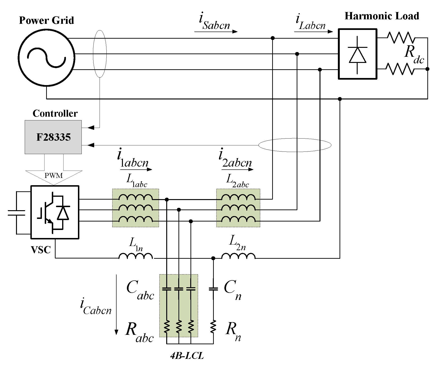
2. System Description and Modeling

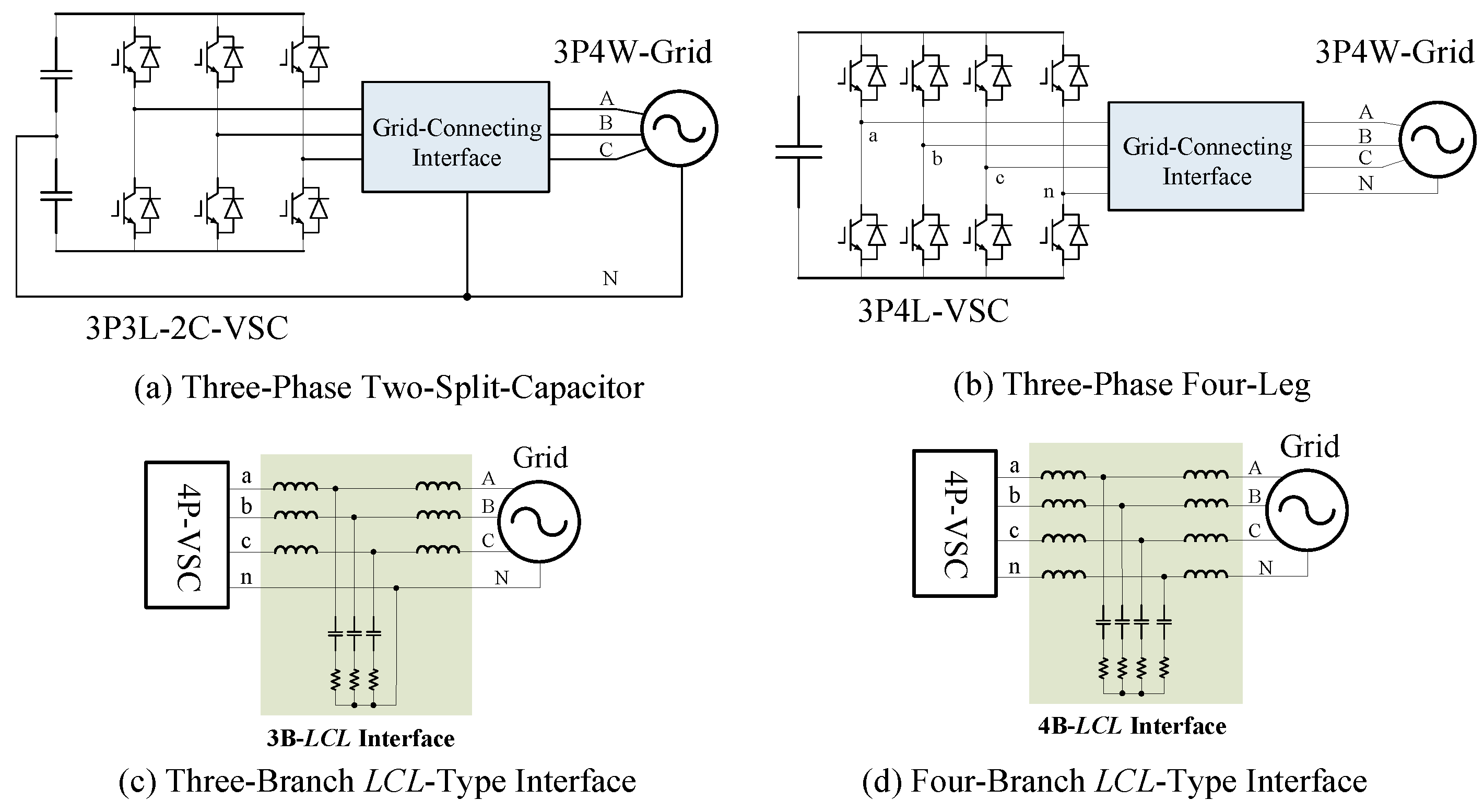
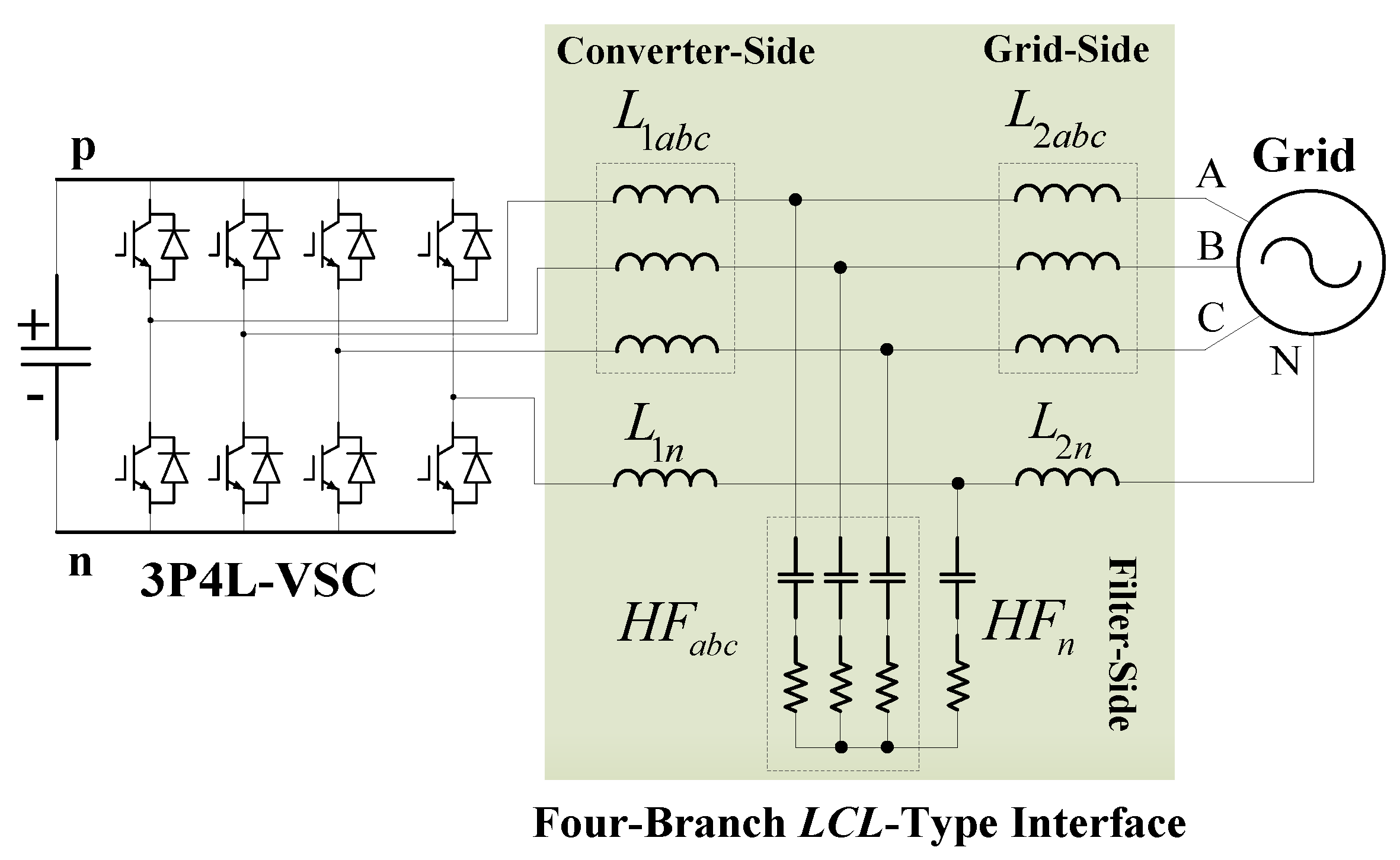
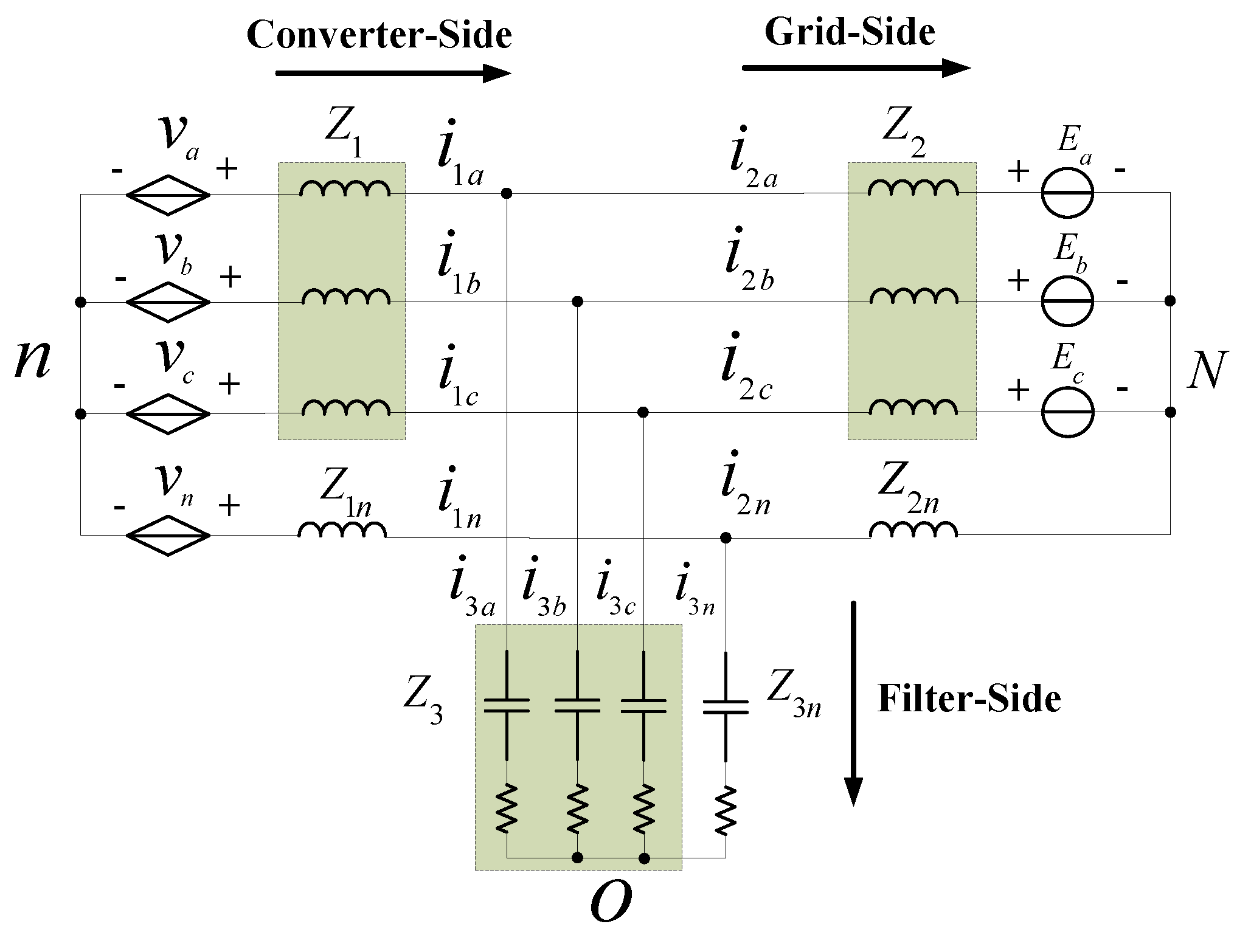
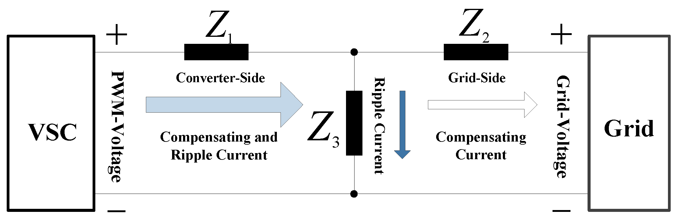
2.1. Topology Description

As illustrated in Figure 2, the proposed four-branch LCL-type interface connects the 3P4L-VSC to the grid utility. L1abc and L2abc, denote the converter-side and grid-side L-R plant, respectively, in phases A, B, and C. HFabc denotes the filter-side R-C plant. L1n, L2n and HFn denote the corresponding elements in phase N.
Figure 2. 3P4L-APF with the proposed 4B-LCL interface.
Energies 08 01606 g002
The functions of the grid-connecting interface can be summarized into two aspects: (1) transforming the VSC output voltage into controllable current injected to the grid with little power loss, and (2) filtering out the so-called current ripple, which is harmonic current around the integral multiples of the switching frequency and is only caused by the PWM-voltage output of 3P4L-VSC.
Compared with the traditional 3B-LCL interface, the proposed topology adopts an additional LCL branch for phase N, which causes a more satisfactory attenuation effect of current ripple and the decoupling for parameter design in phases A, B, C and N. The related details will be provided below.

2.2. Topology Analysis

Figure 3 illustrates the equivalent circuit for topology analysis. Four controlled voltage sources have replaced the four legs of VSC. The analysis of the circuit will be processed in the s domain from two perspectives.
Figure 3. Equivalent circuit.
Energies 08 01606 g003
Z1 and Z2 denote the converter-side and grid-side branch impedance, respectively, in phases A, B, and C. Z1n and Z2n denote the converter-side and grid-side branch impedance, respectively, in phase N. Z3 and Z3n denote the filter-side branch impedance in phases A, B, C and phase N, respectively.

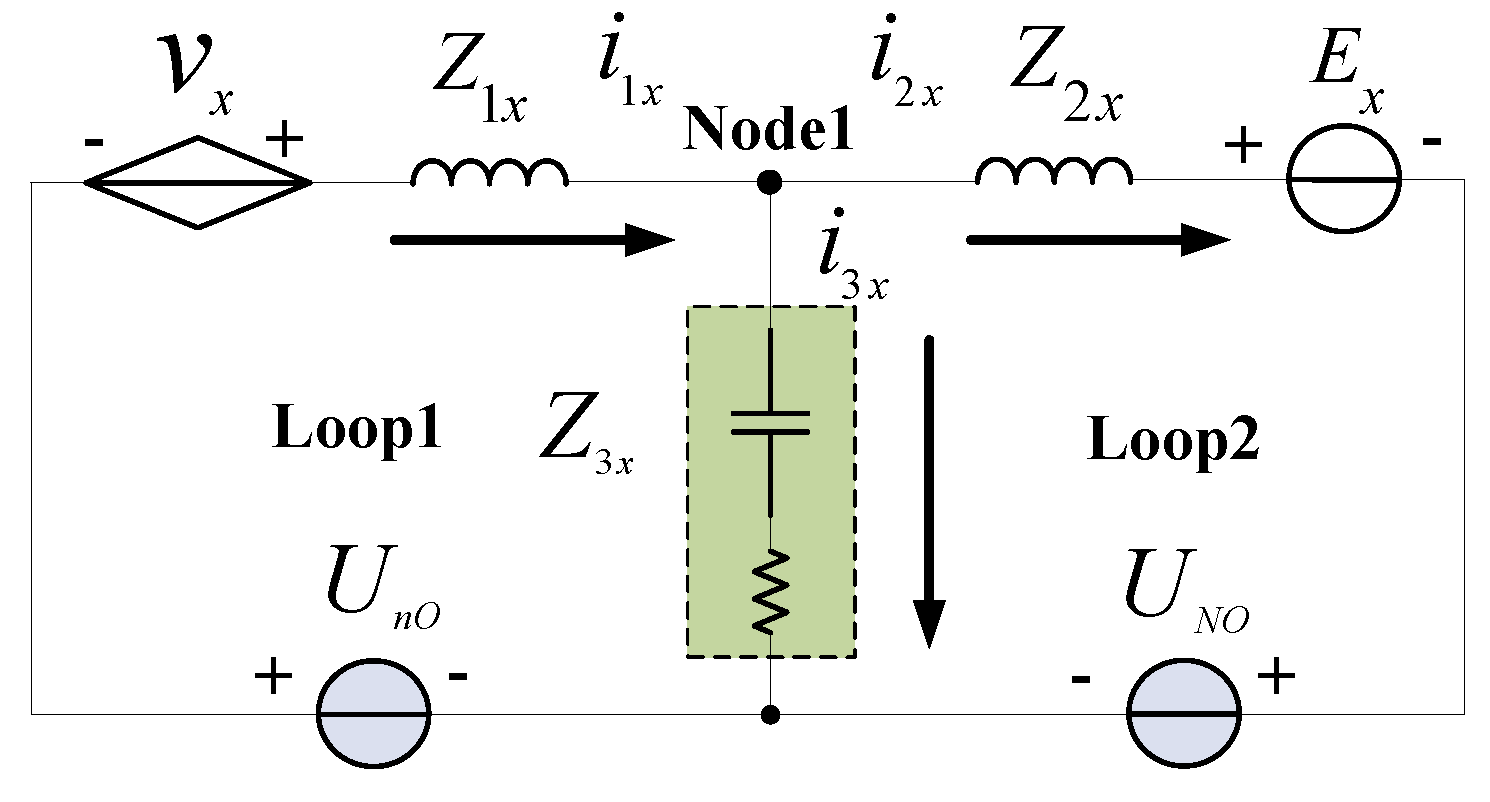
2.2.1. Analysis in the Per-Phase Perspectives

When the voltages between nO and NO are replaced by the voltage sources UnO and UNO, the equivalent circuit in Figure 3 can be divided into four groups in unified form, as shown in Figure 4.
Figure 4. Equivalent circuit in each phase (x = A, B, C, N).
Energies 08 01606 g004
According to the basis theory of circuits, four groups of Equations (1)–(4), can be deduced from Figure 4.
Deduced from Loop 1:
[ I 1 a ( s ) Z 1 a ( s ) I 1 b ( s ) Z 1 b ( s ) I 1 c ( s ) Z 1 c ( s ) I 1 n ( s ) Z 1 n ( s ) ] + [ I 3 a ( s ) Z 3 a ( s ) I 3 b ( s ) Z 3 b ( s ) I 3 c ( s ) Z 3 c ( s ) I 3 n ( s ) Z 3 n ( s ) ] = [ V a ( s ) V b ( s ) V c ( s ) V n ( s ) ] + [ U n O ( s ) U n O ( s ) U n O ( s ) U n O ( s ) ]
Deduced from Loop 2:
[ I 2 a ( s ) Z 2 a ( s ) I 2 b ( s ) Z 2 b ( s ) I 2 c ( s ) Z 2 c ( s ) I 2 n ( s ) Z 2 n ( s ) ] + [ I 3 a ( s ) Z 3 a ( s ) I 3 b ( s ) Z 3 b ( s ) I 3 c ( s ) Z 3 c ( s ) I 3 n ( s ) Z 3 n ( s ) ] = [ E a ( s ) E b ( s ) E c ( s ) E n ( s ) ] + [ U N O ( s ) U N O ( s ) U N O ( s ) U N O ( s ) ]
Deduced from Node 1:
[ I 2 a ( s ) I 2 b ( s ) I 2 c ( s ) I 2 n ( s ) ] = [ I 1 a ( s ) I 1 b ( s ) I 1 c ( s ) I 1 n ( s ) ] [ I 3 a ( s ) I 3 b ( s ) I 3 c ( s ) I 3 n ( s ) ]
Deduced from Nodes n, o, and N:
[ I 1 a ( s ) I 2 a ( s ) I 3 a ( s ) ] + [ I 1 b ( s ) I 2 b ( s ) I 3 b ( s ) ] + [ I 1 c ( s ) I 2 c ( s ) I 3 c ( s ) ] = [ I 1 n ( s ) I 2 n ( s ) I 3 n ( s ) ]
Equations (1) and (2) illustrate that UnO and UNO cause coupling between each phase. Thus, the equivalent circuit in Figure 4 is not suitable for the design of LCL parameters and grid-injecting current control.

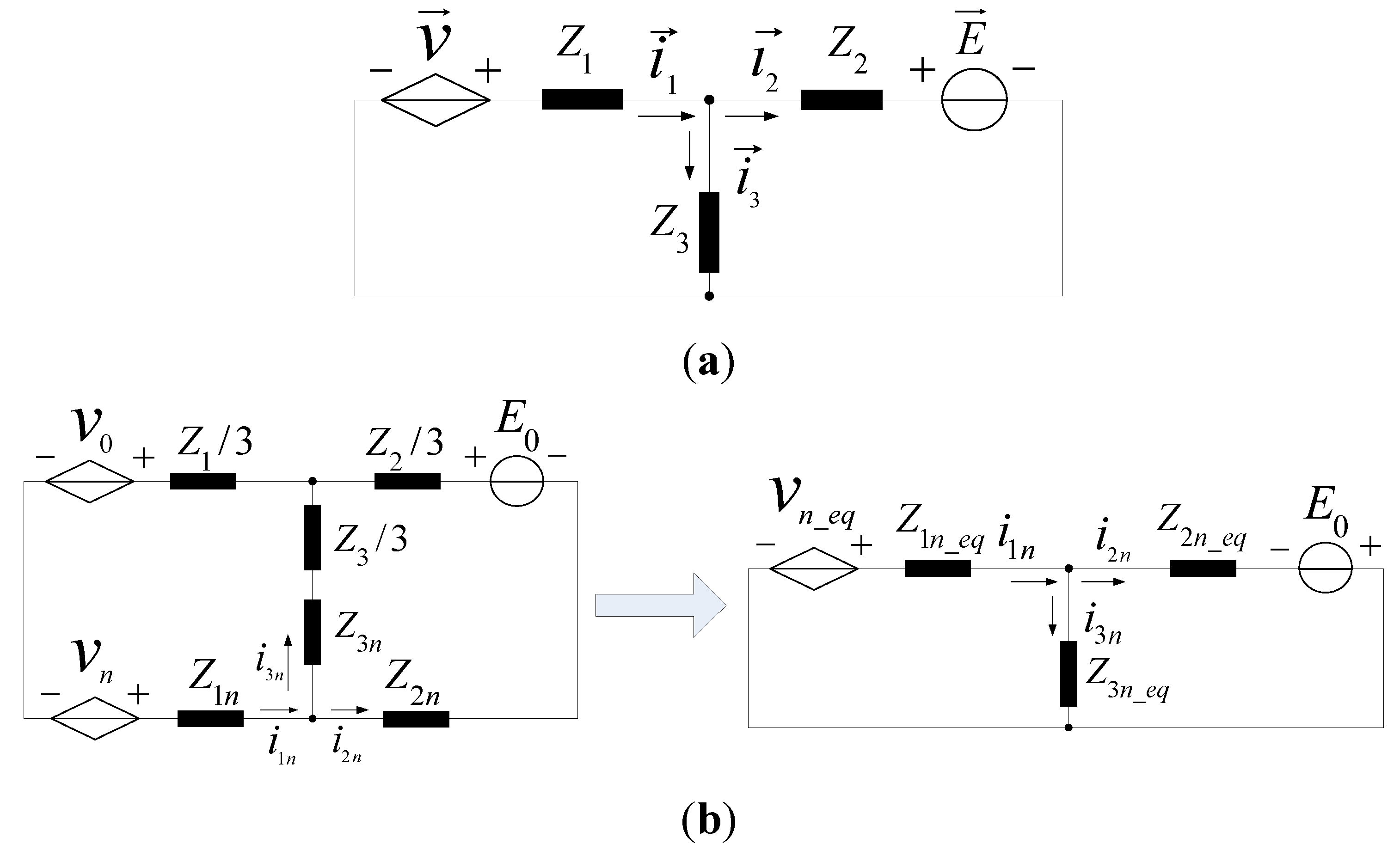
2.2.2. Analysis in the Non-Zero-Sequence and Zero-Sequence Perspectives

To remove UnO and UNO for decoupling, the analysis is processed from the perspectives of non-zero-sequence and zero-sequence, respectively.
The complex vector s-transfer function in Equation (5) for describing the non-zero-sequence circuit can be obtained by conducting symmetrical parameter design in phase ABC and substituting the Clarke transformation matrix 2/3 [1, ej2π/3, e-j2π/3] into both sides of Equations (1)–(3).
{ I 1 ( s ) Z 1 ( s ) + I 3 ( s ) Z 3 ( s ) = V ( s ) I 2 ( s ) Z 2 ( s ) + I 3 ( s ) Z 3 ( s ) = E ( s ) I 2 ( s ) = I 1 ( s ) I 3 ( s )
where
Z 1 ( s ) = Z 1 a ( s ) = Z 1 b ( s ) = Z 1 c ( s ) Z 2 ( s ) = Z 2 a ( s ) = Z 2 b ( s ) = Z 2 c ( s ) Z 3 ( s ) = Z 3 a ( s ) = Z 3 b ( s ) = Z 3 c ( s )
From Equations (1)–(4), the real s-transfer function for the zero-sequence circuit can be obtained as shown in Equation (6).
{ I 1 n ( s ) Z 1 n _ e q ( s ) + I 3 n ( s ) Z 3 n _ e q ( s ) = V n _ e q ( s ) I 2 n ( s ) Z 2 n _ e q ( s ) + I 3 n ( s ) Z 3 n _ e q ( s ) = E 0 ( s ) I 2 n ( s ) = I 1 n ( s ) I 3 n ( s )
where
V n _ e q ( s ) = V n ( s ) V 0 ( s ) Z x n _ e q ( s ) = Z x ( s ) / 3 + Z x n ( s ) ( x = 1 , 2 , 3 )
From Equations (5) and (6), two independent equivalent circuits have been obtained, as illustrated in Figure 5. UnO and UNO have disappeared, which brings the decoupling of each phase. In addition, the left of Figure 5b shows that the additional LCL branch for phase N brings the design of the zero-sequence circuit independent from the non-zero-sequence. Thus, the design of the 4-branch LCL parameter and 4-phase grid-injecting current control becomes the design simply for two independent equivalent circuits in the non-zero-sequence and zero-sequence.
Figure 5. Equivalent circuit in (a) the non-zero-sequence and (b) zero-sequence.
Energies 08 01606 g005

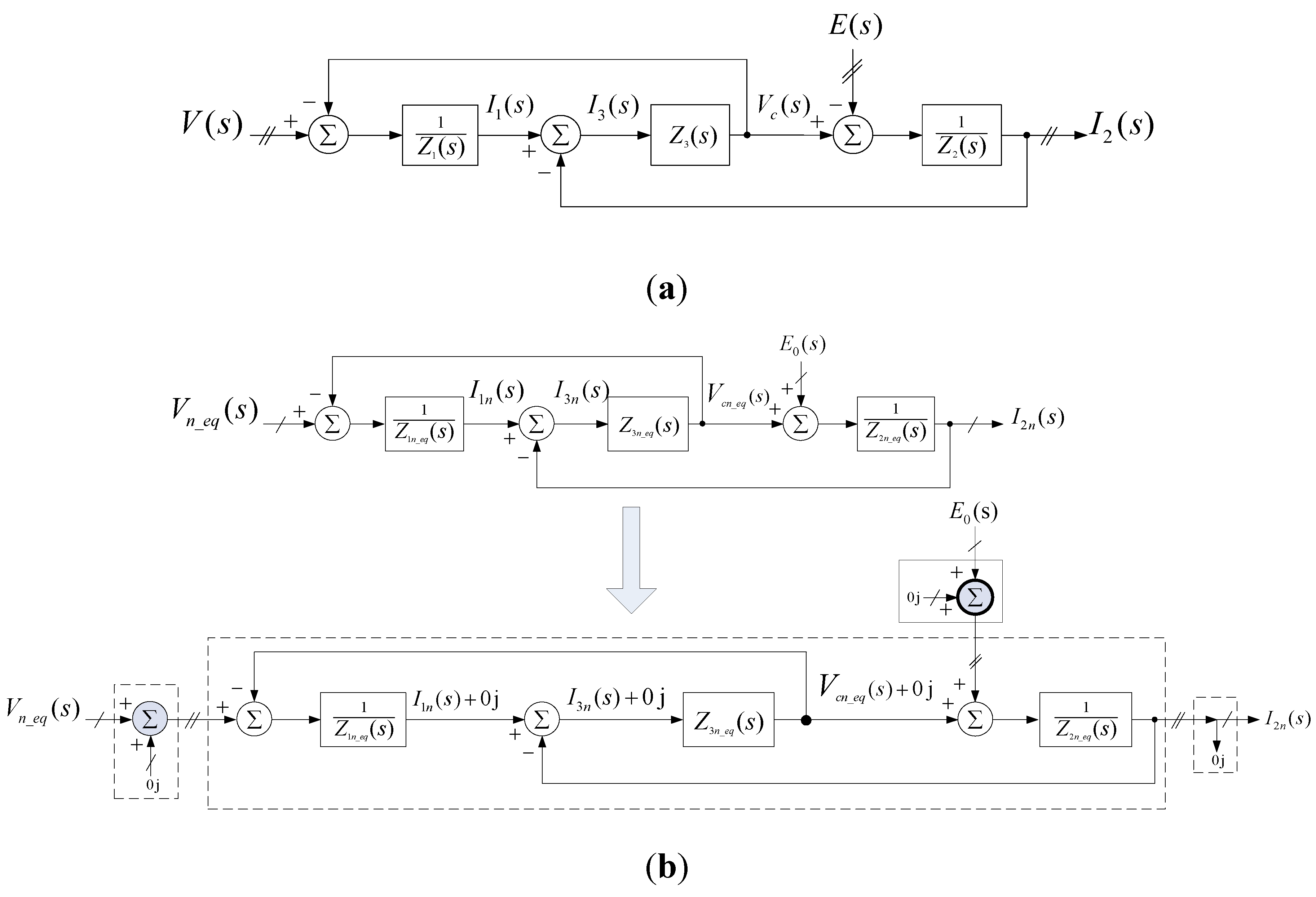
2.3. Model for Parameter Design

Figure 6 illustrates two s-transfer function blocks deduced from the two independent equivalent circuits in Figure 5. When the real signal in the zero-sequence block was regarded as a special complex signal whose imaginary part always equals zero, the two blocks can be entirely in the same style with the unified complex vector form. Furthermore, the s-transfer function matrix can be obtained for the analysis of the characteristic of the LCL circuit, which will be shown in next section.
Figure 6. 4B-LCL model in the (a) non-zero-sequence and (b) zero-sequence.
Energies 08 01606 g006

3. Parameter Design

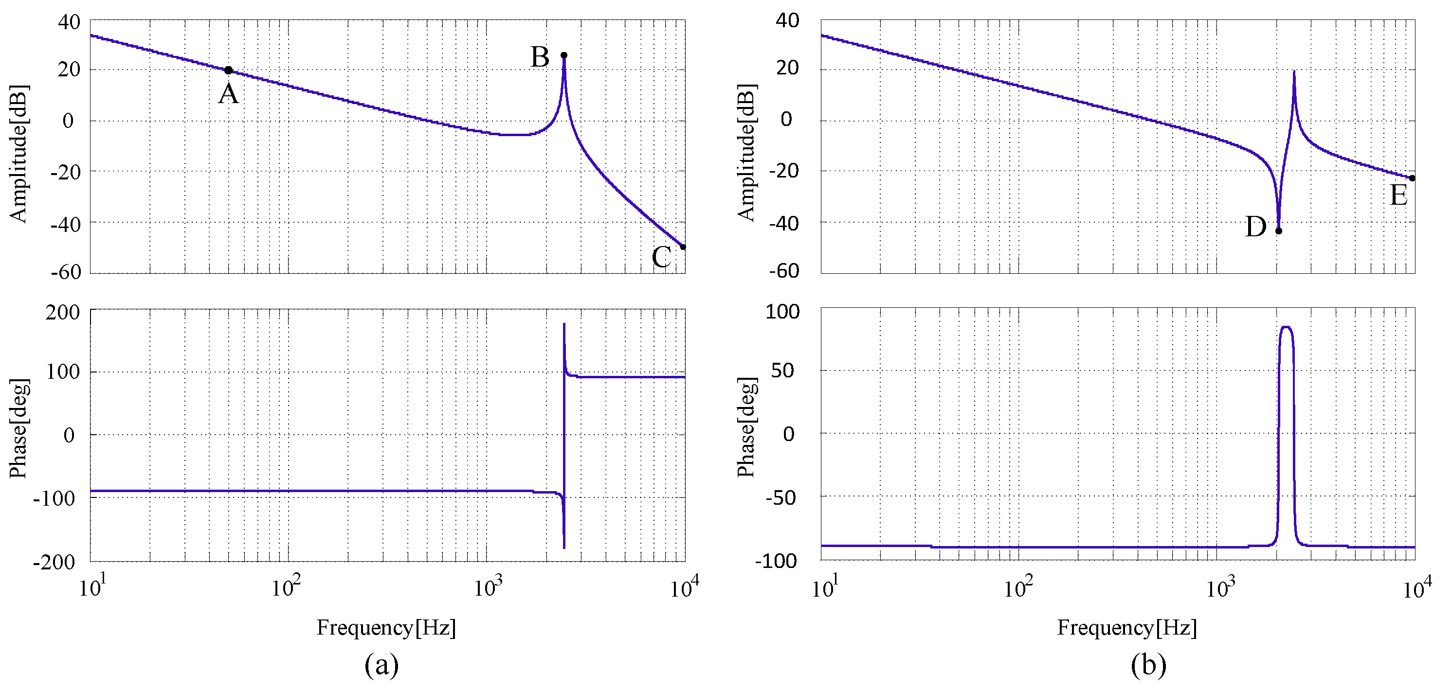
3.1. Circuit Characteristic

The s-transfer function for Matrixes (7) and (8) are deduced from the 4B-LCL complex vector model in the non-zero-sequence and zero-sequence in Figure 6. Because the zero-sequence grid voltage equals approximately zero in practical situations, the zero-sequence concerned is not included in Matrix (8).
[ I 1 ( s ) I 2 ( s ) I 3 ( s ) ] = [ 1 { Z 1 ( s ) + Z 2 ( s ) } ( 1 + Z 1 ( s ) / / Z 2 ( s ) Z 3 ( s ) ) ( 1 + Z 1 ( s ) Z 3 ( s ) ) { Z 1 ( s ) + Z 2 ( s ) } ( 1 + Z 1 ( s ) / / Z 2 ( s ) Z 3 ( s ) ) ( 1 + Z 2 ( s ) Z 3 ( s ) ) { Z 1 ( s ) + Z 2 ( s ) } ( 1 + Z 1 ( s ) / / Z 2 ( s ) Z 3 ( s ) ) 1 { Z 1 ( s ) + Z 2 ( s ) } ( 1 + Z 1 ( s ) / / Z 2 ( s ) Z 3 ( s ) ) Z 2 ( s ) Z 3 ( s ) { Z 1 ( s ) + Z 2 ( s ) } ( 1 + Z 1 ( s ) / / Z 2 ( s ) Z 3 ( s ) ) Z 1 ( s ) Z 3 ( s ) { Z 1 ( s ) + Z 2 ( s ) } ( 1 + Z 1 ( s ) / / Z 2 ( s ) Z 3 ( s ) ) ] [ V ( s ) E ( s ) ]
[ I 1 n ( s ) I 2 n ( s ) I 3 n ( s ) ] = [ 1 { Z 1 n _ e q ( s ) + Z 2 n _ e q ( s ) } ( 1 + Z 1 n _ e q ( s ) / / Z 2 n _ e q ( s ) Z 3 n _ e q ( s ) ) ( 1 + Z 2 n _ e q ( s ) Z 3 n _ e q ( s ) ) { Z 1 n _ e q ( s ) + Z 2 n _ e q ( s ) } ( 1 + Z 1 n _ e q ( s ) / / Z 2 n _ e q ( s ) Z 3 n _ e q ( s ) ) Z 2 n _ e q ( s ) Z 3 n _ e q ( s ) { Z 1 n _ e q ( s ) + Z 2 n _ e q ( s ) } ( 1 + Z 1 n _ e q ( s ) / / Z 2 n _ e q ( s ) Z 3 n _ e q ( s ) ) ] V n _ e q ( s )
where
Z 1 ( s ) = L 1 s + R 1 , Z 2 ( s ) = L 2 s + R 2 , Z 3 ( s ) = 1 / C s + R
Because the s-transfer functions in Matrixes (7) and (8) have a unified form, only the former one has been considered in the circuit characteristic analysis. The bode plots shown in Figure 7 are obtained from Matrix (7), in which L1 = 0.23 mH, L2 = 0.03 mH, C = 30 µF, and R = 0.1 Ω. The two amplitude-frequency curves have the same shape, sharing characteristics of three stages: an initial decrease, followed by an increase and sharp decrease, and finally a continuous decrease.
Figure 7. Bode diagrams (a) I2(s)/V(s), (b) I1(s)/V(s).
Energies 08 01606 g007
Five points will be illustrated in detail as follows; whose values alone fully indicate the performance of the designed LCL circuit. In Figure 7a, point A is in the fundamental frequency corresponding position. Point B is in the peak position. Point C is in the switching frequency position. In Figure 7b, Point D is in the lowest position of the curve. Point E is in the switching frequency position. Two events have occurred in Points B and D, which are the so-called series resonance and parallel resonance. To combine the qualitative and quantitative analyses, four types of impedance s-transfer functions are introduced for further analysis in Equations in (9)–(11).
G 11 ( s ) = { Z 1 ( s ) + Z 2 ( s ) } ( 1 + Z 1 ( s ) / / Z 2 ( s ) Z 3 ( s ) ) ( 1 + Z 2 ( s ) Z 3 ( s ) )
G 22 ( s ) = { Z 1 ( s ) + Z 2 ( s ) } ( 1 + Z 1 ( s ) / / Z 2 ( s ) Z 3 ( s ) ) ( 1 + Z 1 ( s ) Z 3 ( s ) )
G 12 ( s ) = G 21 ( s ) = { Z 1 ( s ) + Z 2 ( s ) } ( 1 + Z 1 ( s ) / / Z 2 ( s ) Z 3 ( s ) )
G11 is the impedance between the PWM voltage and converter-side current, referred to as the converter-side impedance. G22 is the impedance between the grid-voltage and grid-side current, named grid-side impedance. G12 is the impedance between the PWM voltage and grid-side current. G21 is the impedance between the grid-voltage and converter-side current. Because of the symmetry of the LCL circuit, the impedance G21 equals G12. Thus, G21 and G12 are both named the dual-side impedance.
In the proposed impedance perspective, the most comprehensive performance indexes from the designed LCL circuit parameters (L1, L2, C, and R) are described in detail below:
(1) Dual-side impedance amplitude within the output current frequency band:
P 1 = | G 12 | s = j n ω 1 | { Z 1 ( s ) + Z 2 ( s ) } | s = j n ω 1 ( L 1 + L 2 ) n ω 1    ( n = 1 , 2 , 3... N )
This index in (12) (where N is the highest order of the output current frequency) indicates the capacity of an APF with a finite DC voltage and a certain grid voltage at the aspect of the output current’s di/dt, which is referred to as the APF output capacity [12]. A lower impedance amplitude value indicates a higher APF output capacity, and vice versa. In the frequency domain, lower impedance amplitude means higher capacity in outputting high-order frequency current in some other conditions [19]. Because the impedance amplitude is proportional to its frequency within the output current frequency band, the dual-side impedance amplitude in the fundamental frequency is selected for this performance index in practical use, which is (L1 + L2)ω1. A certain APF output capacity requirement corresponds to its upper limit value.
(2) Dual-side impedance amplitude in the switching frequency:
P 2 = | G 12 | s = j ω s | { Z 1 ( s ) Z 2 ( s ) / Z 3 ( s ) } | s = j ω s L 1 L 2 C ω s 3
This index indicates the content of the grid-side current ripple produced by a certain PWM voltage. A smaller grid-side current ripple results in a better performance of the designed LCL [25]. Thus, this principal and critical index should be kept larger than a lower limit.
(3) Converter-side impedance amplitude in the switching frequency:
P 3 = | G 11 | s = j ω s | Z 1 ( s ) | s = j ω s L 1 ω s
This index indicates the content of the converter-side current ripple produced by a certain PWM voltage. Although the converter-side current ripple will be mostly filtered out from injecting into the grid by the filter-side RC-plant (as shown in Figure 8), it is related to some practical considerations: the maximum current of the semiconductor switching devices, the saturation characteristic of the inverter-side inductance, the EMI of the APF, and so on [25]. Thus, this index should be kept larger than a lower limit as well.
Figure 8. Diagram of the current flow path in the LCL circuit.
Energies 08 01606 g008
(4) Series resonant frequency:
ω r e s = 1 L p C
where Lp = L1L2/(L1 + L2)
The index indicates the same series resonant event in both sides of the LCL circuit, which can be considered as the frequency in which the numerator term Zp(s) + Z3(s) in Equations (9)–(11) becomes a real resistor impendence. The index should be selected between the output current upper-limit frequency and half of the controller sampling frequency, which is half of or equal to the switching frequency. In [9], the recommended value is 2ωn< ωres <0.5ωs.
(5) Parallel resonant frequency:
ω 01 = 1 L 2 C
ω 02 = 1 L 1 C
The indexes in Equations (16) and (17) indicate the two parallel resonant events on the converter side and grid side of the LCL circuit, which can be considered as the frequency where the denominator terms Z2(s) + Z3(s) and Z1(s) + Z3(s) in Equations (9)–(10) become a real resistor impendence. Because the direct grid-side current control is adopted commonly, only the index in Equation (17) needs to be considered. A lower index indicates that the high-order background harmonics of the grid voltage have a greater influence over the current controller [19]. Thus, the index should be kept larger than a lower limit value.
(6) Filter-side impedance amplitude in the fundamental frequency:
P 4 = | Z 3 ( s ) | s = j ω 1 1 C ω 1
This index indicates the content of the main fundamental frequency component in the filter-side current produced by the grid voltage, which also mainly consists of the fundamental frequency component. A higher impedance amplitude leads to a lower filter-side current. Thus, this index should be restricted to limit the power loss in the filter-side branch.
(7) Dual-side impedance amplitude in the series resonant frequency:
P 5 = | G 12 | s = j ω r e s ( L 1 + L 2 ) C R ω r e s 2 = R / ( 1 α ) / α
where α = L1/(L1 + L2)
This index indicates the damping effect of the designed LCL circuit directly. A higher impedance amplitude results in a lower peak value of the amplitude-frequency curve in the Bode plots and thus a stronger damping effect. The index is determined by the series resistance R if the total inductance and the capacitance C have been determined. In [25], the recommended value is R < 1/3/C/ωres.

3.2. Design Procedure

The most comprehensive performance indexes have been obtained above. The essential aspect of the LCL parameter design is to meet the performance requirements. Generally, a good performance index will inevitably increase the cost, size, and weight of the LCL components (L1, L2, C or R). Hence, a compromise should be made to keep a balance between performance and cost, size, and weight.
The algorithm for designing the LCL circuit is shown in Figure 9. It contains three tasks: determining the performance index, meeting the performance requirement and verifying the performance index.
Figure 9. Flowchart of the LCL design.
Energies 08 01606 g009

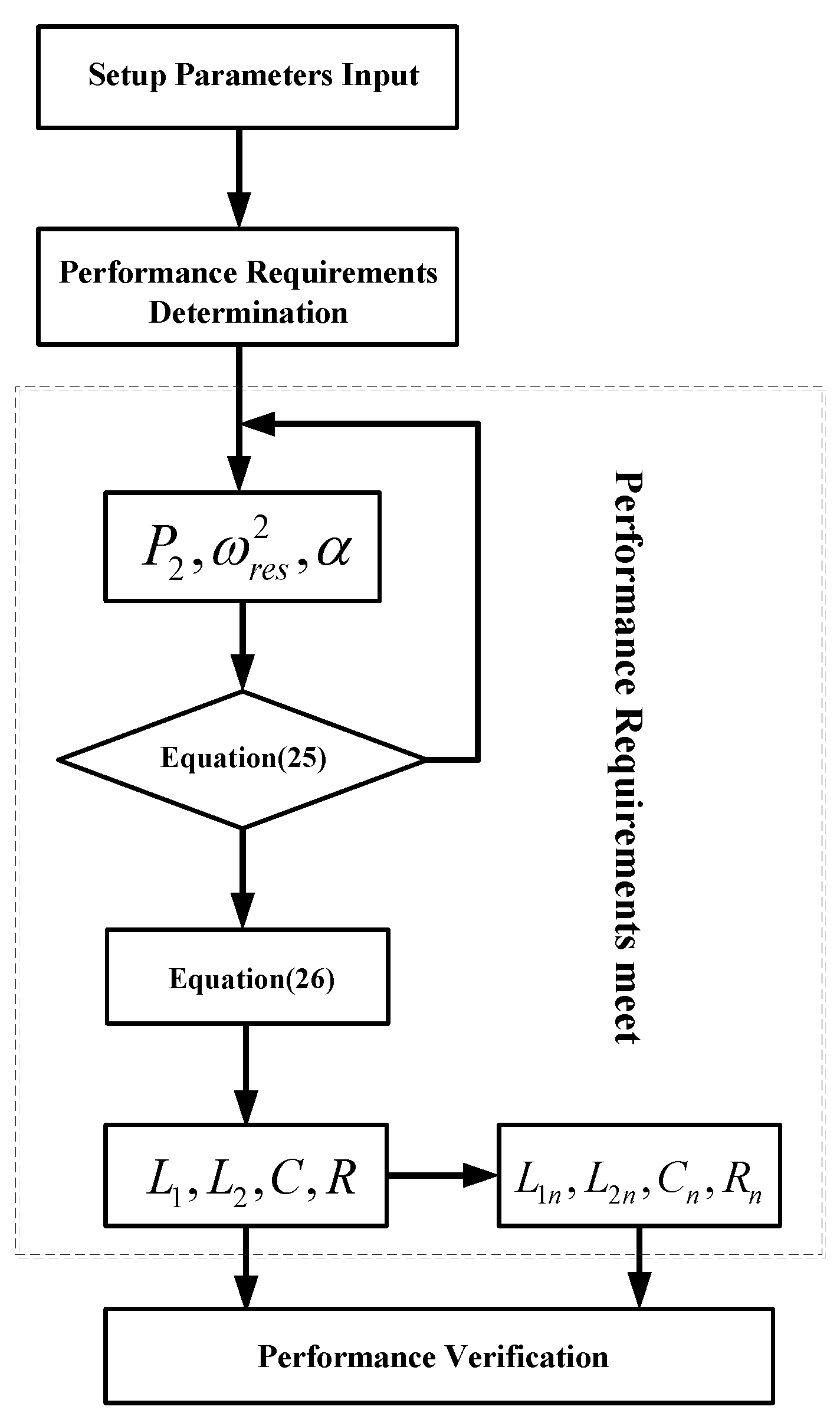
3.2.1. Determination of the Performance Requirements

(1) Calculate the maximum limitation of P1 which is determined by the total inductance L = L1 + L2. To ensure the rated current output capacity of the APF, the following inequality should be satisfied:
I r m s P 1 m V d c n E r m s
where Irms is the rated output current of the APF, Erms is the rms of the grid rated line voltage, n is the ratio of voltage fluctuation (generally 5%–10%), Vdc is the DC-side voltage, and m is the ratio of DC voltage utilization, which is determined by the adopted PWM strategy (e.g., 1/2/ 2 if the per-phase PWM strategy is adopted, 1/ 3 / 2 if the space vector PWM strategy is adopted).
(2) Estimate the maximum value of the PWM voltage ripple in the switching frequency denoted by Vr and further calculate the limitations of P2 and P3 according to Equation (21). The maximum values of the converter-side and grid-side current ripple in the switching frequency are denoted by Ir1 and Ir2. There are various harmonic components in the PWM voltage. The high-frequency harmonic components, which are determined by the type of modulation, DC link voltage, and waveform of the PWM reference voltage (e.g., modulation index), appear on switching and its multiple frequencies, and the uppermost component is around the switching frequency [9]. Vr can also be obtained from the simulation of a practical situation.
{ V r / P 3 I r 1 V r / P 2 I r 2
(3) Determine the range of the series and parallel resonant frequency, which is shown in Equation (22). ωgh is the highest frequency of the grid background harmonics voltage.
{ 2 ω n < ω r e s < 0.5 ω s 2 ω g h < ω 02
(4) Determine the range of the R and C in the filter-side branch according to P4 and P5. Ic1 is the maximum fundamental frequency current in the filter-side branch, which is caused by the grid. P5 should be above one for the close-loop control stability [12]. Thus, the range of R is obtained via Equation (24).
E 1 / P 4 < I c 1
α ( 1 α ) < R < 1 3 C ω r e s

3.2.2. Meeting the Performance Requirements

The inequality in Equation (25) can be obtained based on Equations (20)–(24). According to the flowchart of the LCL design in Figure 9, the LCL parameters can be determined by a simple trial-and-error process. The essential aspect of the process is utilizing the performance indexes P2, ωres and α to deduce the proper L1, L2, C, R that can meet the inequality in Equation (25) and reach the optimal target, which is to maximize P2/L.
{ P 2 P 2 min 1 4 ω n 2 ω r e s 2 4 ω s 2 1 > α 0.5 P 1 = ω r e s 2 P 2 ( ω 1 ω s 3 ) P 1 max P 3 = ω r e s 2 P 2 α ( 1 ω s 3 ) P 3 min P 4 = α ( 1 α ) ω r e s 4 P 2 ( 1 ω s 3 ω 1 ) P 4 min ω 01 2 = ω r e s 2 ( 1 α ) 4 ω g h 2
{ L 1 = ω r e s 2 P 2 α ( 1 ω s 3 ) L 2 = ω r e s 2 P 2 ( 1 α ) ( 1 ω s 3 ) C = ω s 3 α ( 1 α ) ω r e s 4 P 2 1 3 C ω r e s > R > α ( 1 α )

3.2.3. Verification of the Performance Index

The LCL performance index output table should be contained in an integral LCL design procedure for the design specification. Additionally, the selected parameters in a practical situation may differ from the calculated ones. Thus, a practical performance index output table is necessary.

4. Simulation

The simulation model is established in MATLAB/Simulink. The purpose of the simulation is to verify the current ripple filtering effect of the designed 4B-LCL; therefore, it is carried out by the open-loop method excluding the APF’s controller. The parameters of the designed 4B-LCL are obtained by the method mentioned above. All simulation parameters are shown in Table 1, Table 2, Table 3 and Table 4.
Table 1. Setup parameters.
SymbolQuantityValue
ErmsPhase grid voltage200–240 V
fghHighest background voltage harmonics frequency550 Hz
hHighest frequency order of the output current harmonics20
mDC Voltage Utilization Ratio1/ 3 / 2
VdcDC Link Voltage800 V
fsSwitching Frequency10 KHz
IrmsRated Output Current in phases A, B, C, and N100 A
Ir1Converter-side current ripple rms in phases A, B, C, and N≤12 A
Ir2Grid-side current ripple rms in phases A, B, C, and N≤1 A
Table 2. Table of performance requirements in phases A, B, C, and N.
SymbolQuantityValue
P1Dual-side impedance amplitude in the fundamental frequency≤0.87 Ω
P2Dual-side impedance amplitude in the switching frequency≥295.2 Ω
P3Converter-side impedance amplitude in the switching frequency≥10.0 Ω
P4Filter-side impedance amplitude in the fundamental frequency≥40.0 Ω
P5Dual-side impedance amplitude in the series resonant frequencyapproximately 1.0 Ω
fresDual-side series resonant frequency[2.0 KHz, 5.0 KHz)
f01Grid-side parallel resonant frequency[1.1 KHz, fres)
Table 3. Parameters selected and its performance index in phases A, B, and C.
SymbolQuantityValue: the selected (the calculated)
L1Converter-side inductance0.23 mH (0.273 mH)
L2Grid-side inductance0.10 mH (0.086 mH)
CFilter-side capacitance60 µF (56.92 µF)
RFilter-side resistance0.2 Ω (0.196 Ω)
P1Performance Index Output in phases A, B, and C0.1 Ω
P2301.0 Ω
P314.2 Ω
P453.1 Ω
P50.93 Ω
fres2.46 KHz
f012.05 KHz
Table 4. Parameters selected and its performance index in phase N.
SymbolQuantityValue: the selected (the calculated)
L1nConverter-side inductance0.32 mH (0.312 mH)
L2nGrid-side inductance0.14 mH (0.138 mH)
CnFilter-side capacitance42 µF (41.74 µF)
RnFilter-side resistance0.15Ω (0.145 Ω)
L1n_eqEquivalent Value in phase N0.40 mH
L2n_eq0.16 mH
Cn_eq33.53 µF
Rn_eq0.21 Ω
P1nPerformance Index Output in phase N0.028 Ω
P2n559.4 Ω
P3n19.2 Ω
P4n94.88 Ω
P5n1.23 Ω
fres_n2.53 KHz
f01_n2.21 KHz

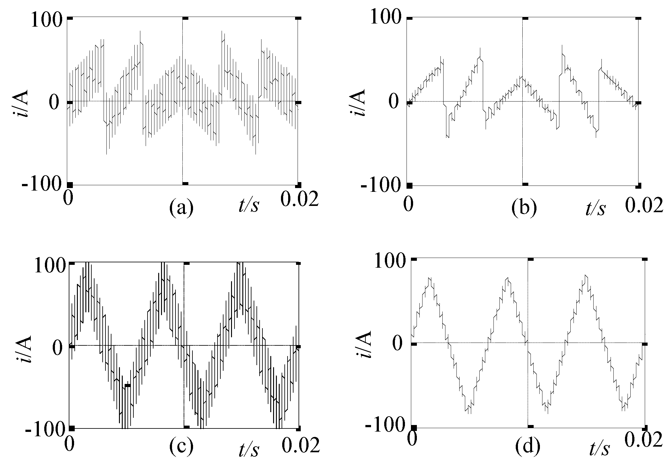
4.1. Current Ripple Filtering in Different PWM Voltage Modulation Indexes

Table 5 illustrates that the magnitude of the switching frequency output voltage ripples is inversely proportional to the modulation index. With the increase of the modulation index, the grid-side current ripple of the switching frequency was reduced steadily. When the index is 1.0, by installing the proposed 4B-LCL interface, the switching frequency ripple currents in phases A and N have been reduced from 12.13 A and 20.65 A to 0.21 A and 0.84 A, respectively, which has provided great filtering results.
Table 5. Results of the current ripple filtering in different PWM voltage modulation indexes.
PWM VoltageSwitching frequency current rms/ADamping resister power loss (w)
Modulation indexSwitching frequency voltageConverter-side (A,N)Grid-side (A,N)
0.0357.93, 600.9390.04, 120.334.09, 6.041632 W
0.2300.12, 463.4660.02, 98.123.09, 5.83800 W
0.4260.34, 300.6250.17, 70.582.09, 3.92300 W
0.6190.83, 263.9130.18, 50.111.09, 1.9393 W
1.090.34, 220.4612.13, 20.650.21, 1.1921 W
Figure 10 shows the simulation waveforms indicating the ripple current filtering effect by the designed 4B-LCL interface.
Figure 10. Comparison between converter-side and grid-side current in phases A and N. (a) and (c) show the current waveforms in the converter side in phases A and N. (b) and (d) show the current waveforms in the grid side in phases A and N. The figure clearly shows the filtering effect by the proposed 4B-LCL interface. The grid-side current waveform is considerably smoother than that of the converter side.
Energies 08 01606 g010

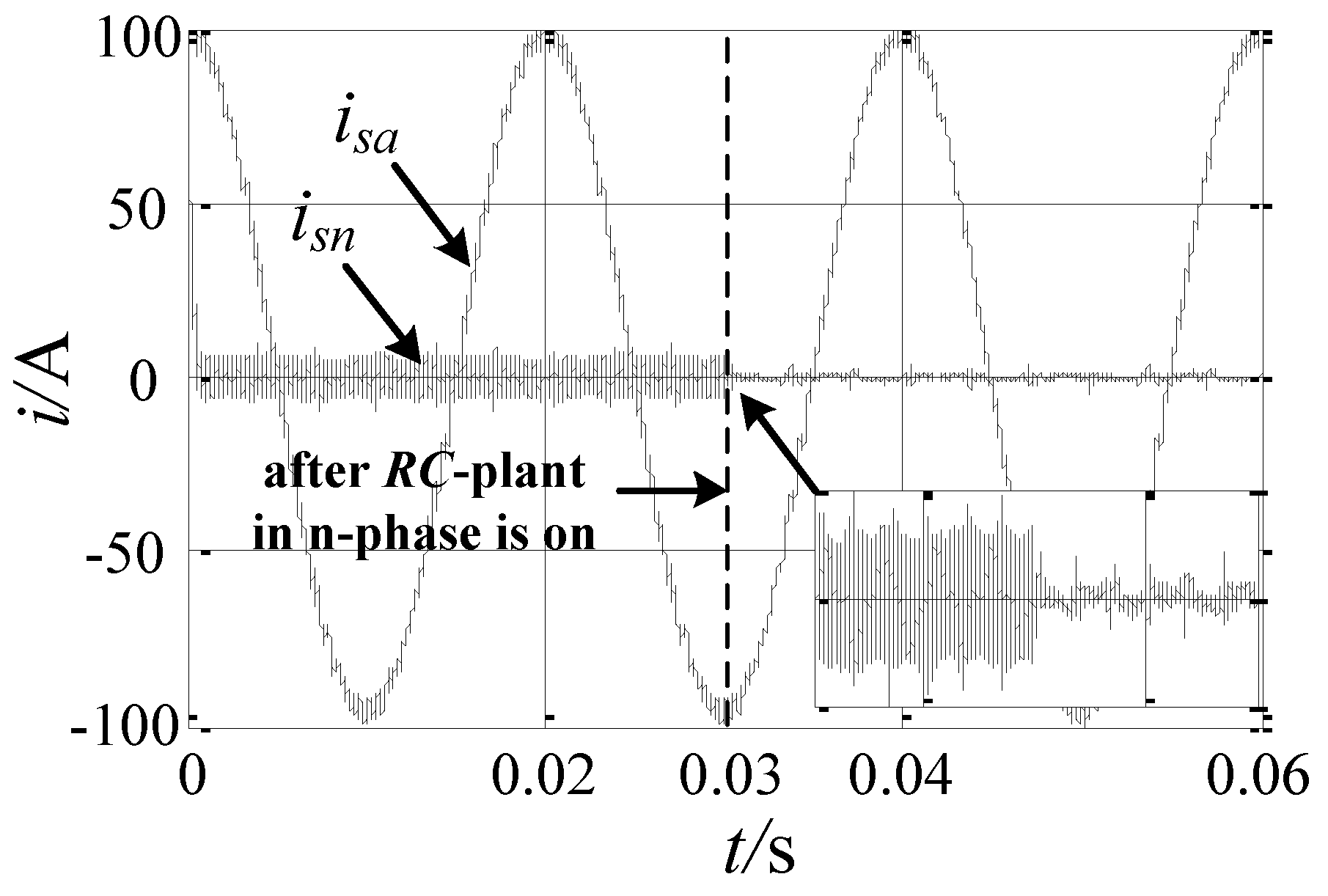
4.2. Current Ripple Filtering by the LCL Branch in Phase N

Figure 11 shows the grid-side current waveforms of phase N at the RC-plant switching time. It can be seen that isa and isn have many high frequency current ripples before the RC-plant in n-phase has been switched on, but the high frequency current ripples have almost disappeared after it has been switched on. In particular, the current ripple in isn has been decreased from 10 A–0.9 A. This result verifies the good effect on current ripple filtering of the LCL-branch in phase N.
Figure 11. Comparison with and without the LCL branch in phase N.
Energies 08 01606 g011

5. Experimental Results

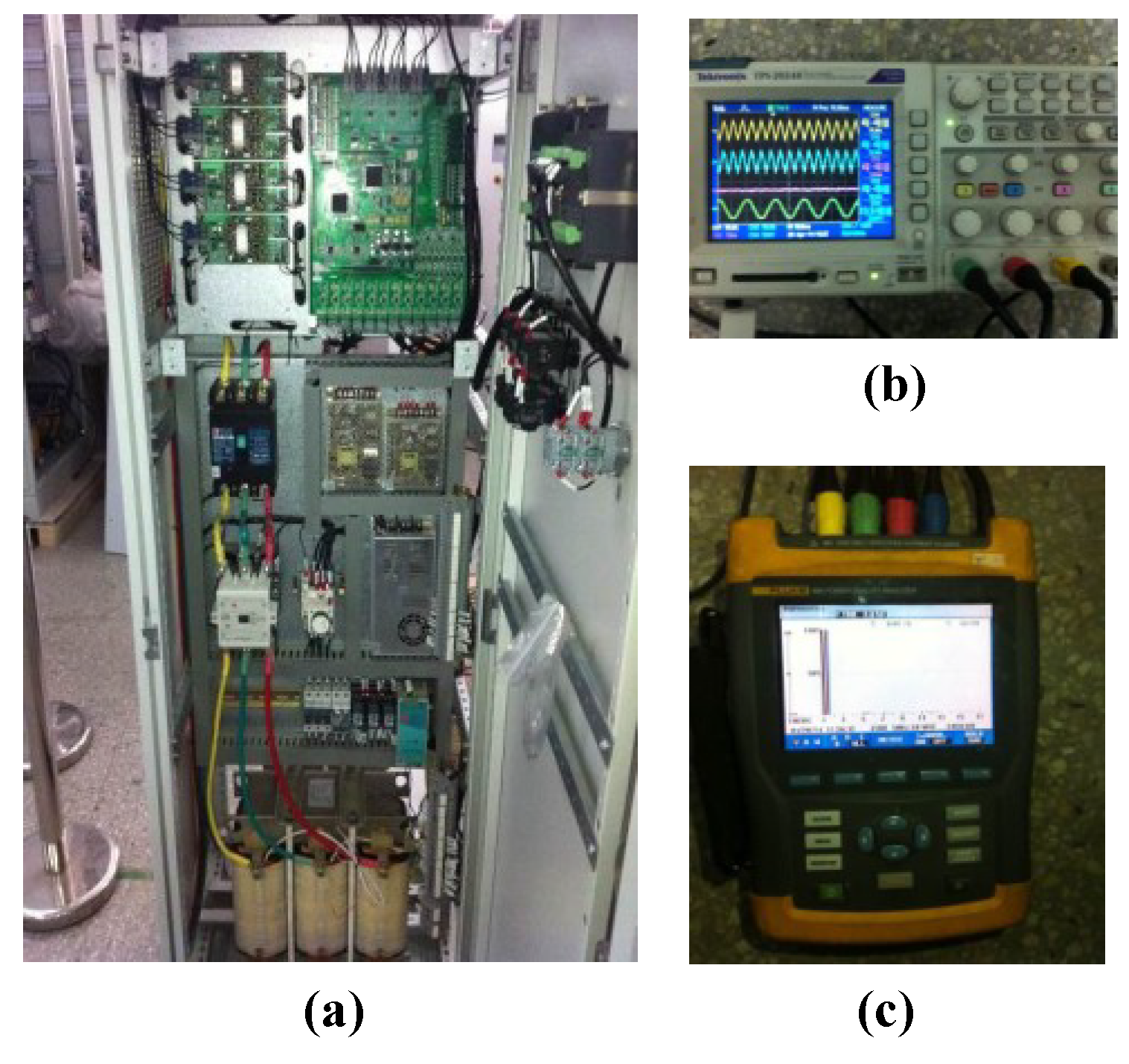
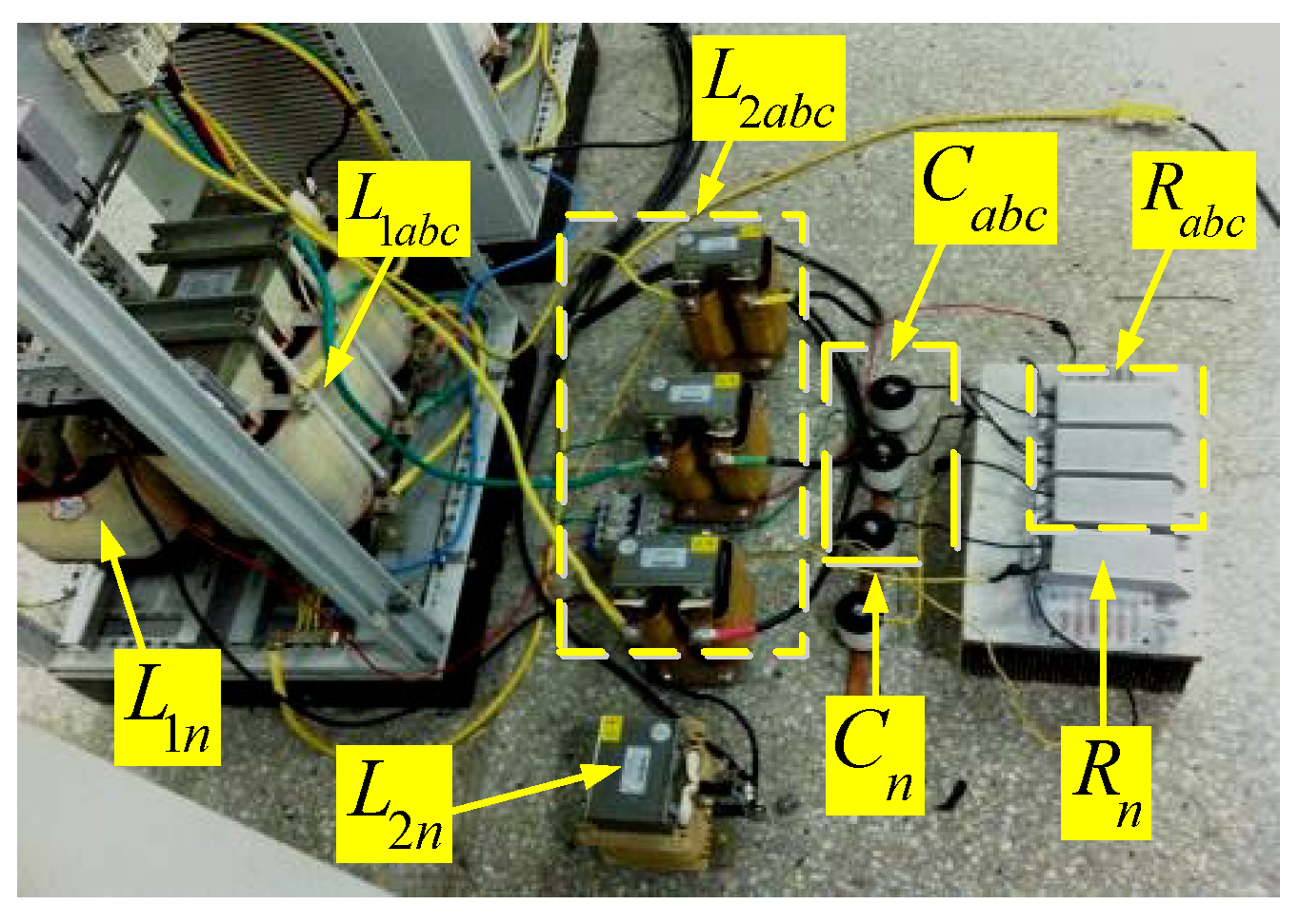
5.1. Experimental Platform

Figure 12a shows the experimental platform, where SKM400GB176D from SEMIKRON was selected as the power module IGBT, and TMS320F28335 from Texas Instruments was selected as the main controller chip for digital signal processing. In addition, the platform has adopted the power quality analyzer (Fluke 434B) and Oscilloscope (Tektronix 2024B) as measurement instruments in Figure 12b,c. The actual 4B-LCL circuit implemented is shown in Figure 13.
Figure 12. Experimental platform and measurement instruments.
Energies 08 01606 g012
Figure 13. Implemented 4B-LCL circuit.
Energies 08 01606 g013
Figure 14. Experimental system.
Energies 08 01606 g014
The experimental system consists of the controller, voltage source converter (VSC), harmonic load, three-phase four-wire power grid, and proposed four-branch (4B) LCL grid-connecting interface, as shown in Figure 14. The APF controller sampled the grid-side current to directly regulate the output current, which is injected into the grid to fully compensate for the load current harmonics. The harmonic load was modified from the typical three-phase uncontrolled rectifier bridge, where the midpoint of the resistors on the DC side was connected to phase N of the power grid for the purpose of getting the current harmonics in this phase. In addition, the parameters of the experiment are the same as in the simulation above.

5.2. Experimental Results

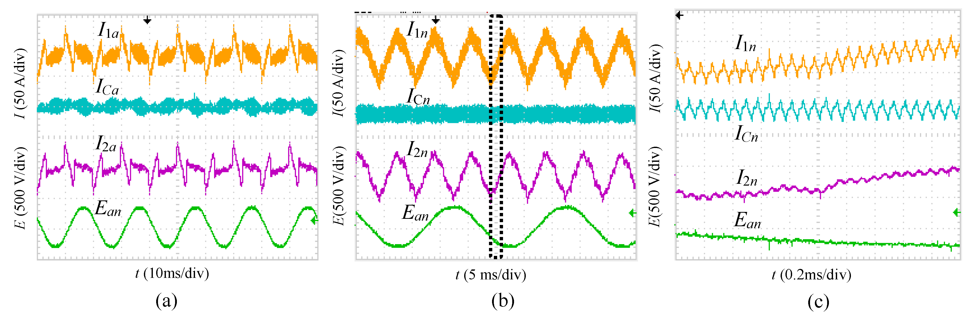
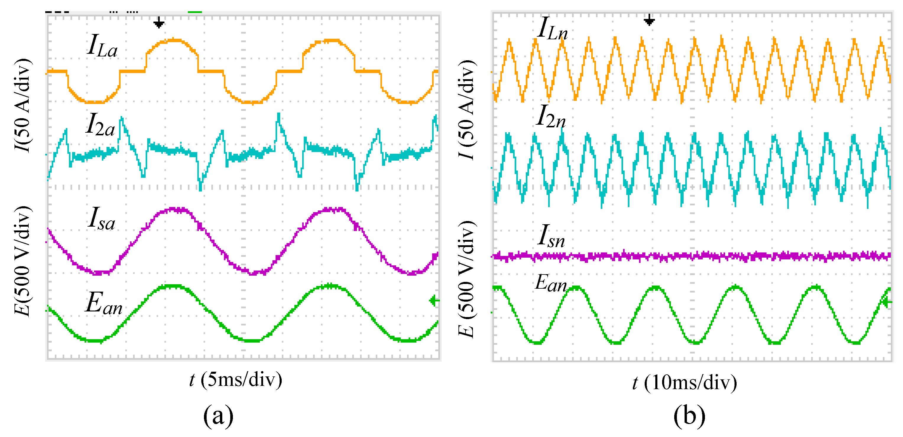
5.2.1. Current Ripple Filtering

Figure 15a,b show the current waveforms of the proposed 4B-LCL in phase A and N, when the APF is fully compensating the load current harmonics. In this figure, I1a & I1n, ICa & ICn, I2a & I2n, and Ean are the converter-side current, filter-side current, grid-side current, and grid voltage, respectively, between phases A and N. Because the three phases are symmetric, it is not necessary to demonstrate the waveforms in phases B and C. These waveforms illustrate that I1a & I1n have a massive high-frequency current ripple, which has been filtered out into Ica & Icn. I2a & I2n have a smoother waveform than I1a & I1n. Furthermore, Figure 15c is a zoomed-in view of the dashed box in Figure 15. The period of the high-frequency ripple wave in I1n and ICn is approximately 0.1 ms (which is just the switching period of IGBT), and their amplitudes are nearly identical. The current ripple of the grid-side current I2n has been greatly reduced, and the waveform of the grid voltage Ean is also extremely smooth. Therefore, the designed 4B-LCL has obtained a good performance in the current ripple filtering.
Figure 15. Waveforms of the 4B-LCL (a) in phase A (b) in phase N (c) Zoomed-in view.
Energies 08 01606 g015
Figure 16a,b show the FFT results of the converter-side and grid-side current in phase N. A large amount of current ripples around the switching frequency are contained in the converter-side current. The ripple content reaches approximately 32 dB at the switching frequency fs and 3fs, whereas that in the grid-side current has been evidently reduced to approximately 10 dB around fs and to a negligible level around other integral multiples of fs. This experimental result has further verified the current ripple reduction effect in phase N of the designed 4B-LCL circuit.
Figure 16. FFT of the current in phase N (a) converter-side (b) grid-side.
Energies 08 01606 g016

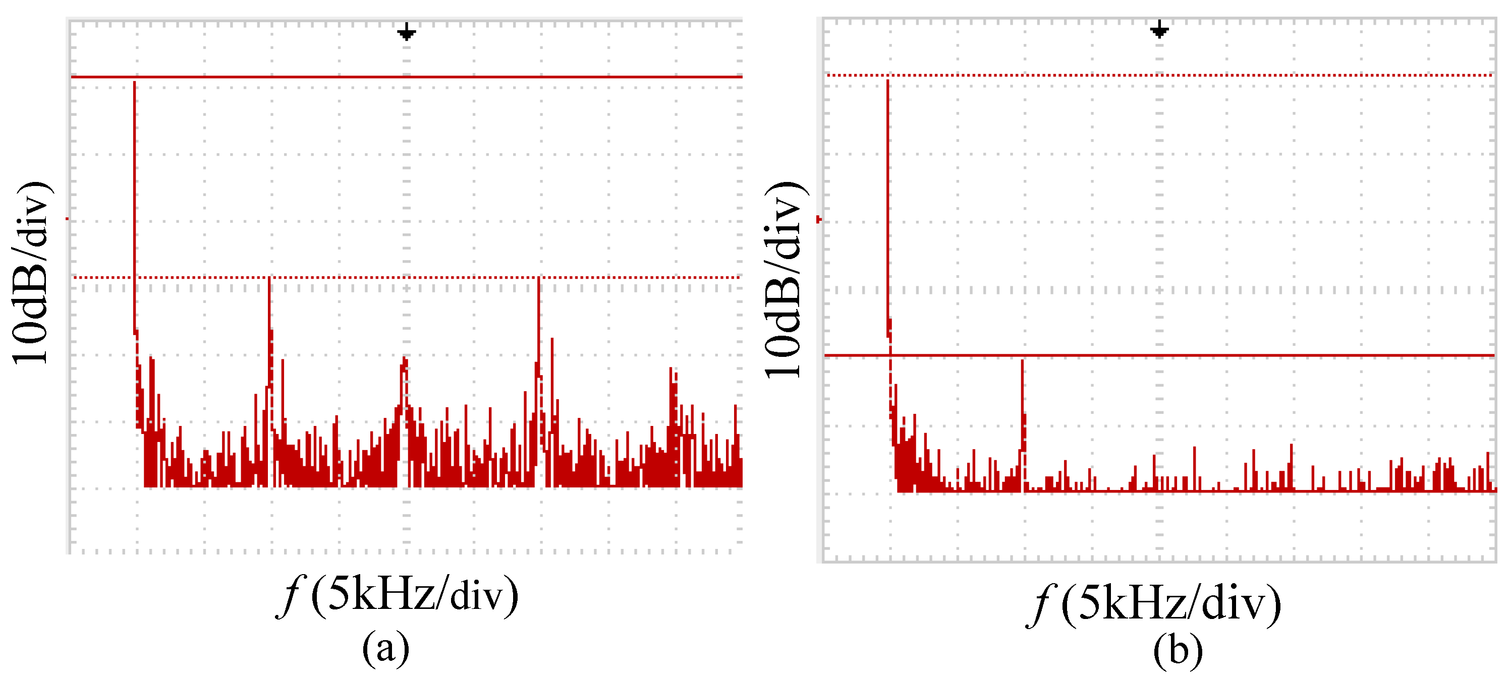
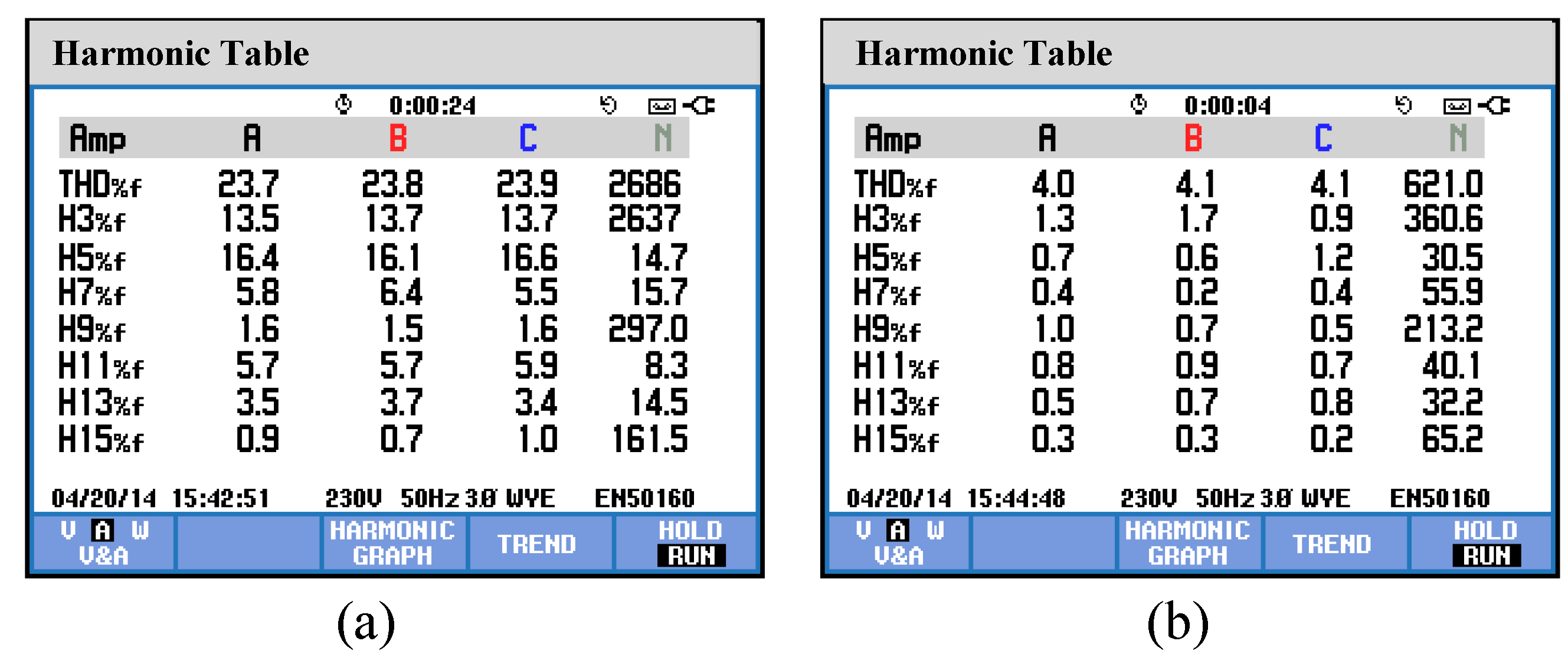
5.2.2. Harmonic Compensation

Figure 17a,b are the current waveforms in phase A and N when the APF is fully compensating the load current harmonics. ILa & ILn, I2a & I2n, ISa & ISn are the load current, compensating current, and grid current, respectively, in phases A and N. Ean is the grid voltage between phases A and N. In Figure 17a, the load current ILa is considerably distorted. However, the grid current ISa has a good sinusoidal waveform due to the compensating current I2a. In Figure 17b, the period of the load current ILn in phase N is approximately 7 ms, which indicates the existence of a large amount of the third harmonic current. The compensating current I2n from the APF almost equals the lode current ILn in both amplitude and phase. Thus, the grid current in phase N is approximately zero, which means that the current harmonics in phase N are well compensated.
Figure 17. Waveforms in harmonic compensation (a) in phase A (b) in phase N.
Energies 08 01606 g017
Figure 18a,b shows the THD and ratio of harmonic frequency content in the load current and grid current. The current THD dropped from 23.7%, 23.8%, and 23.9% in the load current to 4.0%, 4.1%, and 4.1%, respectively, in the grid current. The experimental result has met the requirement of THD in GB/T 14549-93. Each frequency harmonic distortion has dropped from over 1% in the load current to below 1% in the grid current. The good harmonic compensation result has further verified the effectiveness of the designed 4B-LCL grid-connecting interface.
Figure 18. Harmonic forms of the (a) load current and (b) grid current.
Energies 08 01606 g018

6. Conclusions

Based on an analysis via mathematical models for decoupling and the most comprehensive performance indexes in the proposed impedance perspective, this paper has proposed a four-branch LCL-type grid-connecting interface and detailed parameter design procedure for a three-phase, four-leg active power filter. This paper focuses on two aspects: (1) describing the mathematical models of 4B-LCL in the full complexity vector form from the zero and non-zero sequence perspectives, resulting in two independent and uniform equivalent circuits without cross-coupling terms; (2) proposing the 4B-LCL parameter design method based on the most comprehensive performance index, including three main stages as the specification: performance requirements determination, fulfillment and verification. The Simulink results established in MATLAB and the experimental results obtained from the APF platform with the 4B-LCL type grid-connecting interface demonstrate that the 4B-LCL interface yields better current ripple filtering performance, which verifies the validity and effectiveness of the proposed design method.

Acknowledgments

This work is supported in part by grants from the National Natural Science foundation of China (Project No. 51477030), Innovation foundation for Combination of Industry and Scientific Research of Jiangsu Province, China (Project No. BY2014127-15).

Author Contributions

Wu Cao and Jianfeng Zhao designed the research; Wu Cao and Kangli Liu performed the research; Wu Cao, Yongchao Ji and Yigang Wang wrote the paper. All authors read and approved the final manuscript.

Conflicts of Interest

The authors declare no conflict of interest.

References

  1. Grino, R.; Cardoner, R.; Costa-Castello, R.; Fossas, E. Digital repetitive control of a three-phase four-wire shunt active filter. IEEE Trans. Ind. Electron. 2007, 54, 1495–1503. [Google Scholar] [CrossRef]
  2. Montero, M.; Cadaval, E.; Gonzalez, F. Comparison of control strategies for shunt active power filters in three-phase four-wires systems. IEEE Trans. Power Electron. 2007, 22, 229–236. [Google Scholar] [CrossRef]
  3. Le, J.; Jiang, Q.R.; Han, Y.D. The analysis of hysteresis current control strategy of three-phase four-wire APF based on the unified mathematic model. In Proceedings of the CSEE, Harbin, China, 23–25 May 2007; IEEE: Piscataway, NJ, USA, 2007; pp. 85–91. [Google Scholar]
  4. Kanaan, H.Y.; Georges, S.; Mendalek, N.; Hayek, A.; Al-Haddad, K. A linear decoupling control for a PWM three-phase four-wire shunt active power filter. In Proceedings of the Electro Technical Conference, Ajaccio, France, 5–7 May 2008; IEEE: Piscataway, NJ, USA, 2008. [Google Scholar]
  5. Petterson, S.; Salo, M.; Tuusa, H. Applying an LCL-filter to a four-wire active power filter. In Proceedings of the Power Electronics Specialists Conference, Jeju, Korea, 18–22 June 2006; IEEE: Piscataway, NJ, USA, 2006. [Google Scholar]
  6. Khadkikar, V.; Chandra, A.; Singh, B. Digital signal processor implementation and performance evaluation of split capacitor, four-leg and three H-bridge-based three-phase four-wire shunt active filters. IET Power Electron. 2011, 4, 463–470. [Google Scholar] [CrossRef]
  7. Lin, J.Y.; Wang, Z.S.; Chen, H.M.; Li, C. High performance controller design for three-phase four-leg inverters. CSEE 2007, 27, 101–105. [Google Scholar]
  8. Hirve, S.; Chatterjee, K.; Fernandes, B.G.; Imayavaramban, M.; Dwari, S. PLL-less active power filter based on one-cycle control for compensating unbalanced loads in three-phase four-wire system. IEEE Trans. Power Del. 2007, 22, 2457–2465. [Google Scholar] [CrossRef]
  9. Le, J.; Liu, K.P.; Tan, T.Y. A novel compound switching control strategy of the 4-leg shunt active power filter. CSEE 2011, 36, 62–70. [Google Scholar]
  10. Guo, W.F.; Xu, D.G.; Wu, J.; Wang, L.G. Novel control method for LCL active power filter. CSEE 2010, 30, 42–48. [Google Scholar]
  11. Liu, F.; Zha, X.M.; Duan, S.X. Design and research on parameter of LCL filter in three-phase grid-connected inverter. Trans. China Electr. Tech. Soc. 2010, 25, 110–116. [Google Scholar]
  12. Liu, Q.; Peng, L.; Kang, Y.; Tang, S.Y.; Wu, D.L.; Qi, Y. A novel design and optimization method of an LCL filter for a shunt active power filter. IEEE Trans. Ind. Electron. 2014, 61, 4000–4010. [Google Scholar] [CrossRef]
  13. Chen, Y.; Jin, X.M.; Tong, Y.B. Grid-side LCL-filter of three-phase voltage source PWM rectifier. Trans. China Electr. Tech. Soc. 2007, 22, 124–129. [Google Scholar]
  14. Wang, Y.Q.; Wu, F.J.; Sun, L.; Sun, Q. Optimized design of LCL filter for minimal damping power loss. CSEE 2010, 30, 90–95. [Google Scholar]
  15. Ahmed, K.H.; Finney, S.J.; Williams, B.W. Passive filter design for three-phase inverter interfacing in distributed generation. In Proceedings of Compatibility in Power Electronics, Gdansk, Poland, 29 May–1 June 2007; IEEE: Piscataway, NJ, USA, 2007. [Google Scholar]
  16. Wu, J.; Ma, X.; Hou, R.; Xu, D.G. Optimization of APF LCL output filter based on genetic algorithm. Trans. China Electr. Tech. Soc. 2011, 26, 159–164. [Google Scholar]
  17. Shri, A.; Popovic, J.; Ferreira, J.A.; Gerber, M.B. Design and control of a three-phase four-leg inverter for solid-state transformer applications. In Proceedings of Power Electronics and Applications, Lille, France, 2–6 September 2013; IEEE: Piscataway, NJ, USA, 2013. [Google Scholar]
  18. Gabe, I.J.; Montagner, V.F.; Pinheiro, H. Design and implementation of a robust current controller for VSI connected to the grid through an LCL filter. IEEE Trans. Power Electron. 2009, 24, 1444–1452. [Google Scholar] [CrossRef]
  19. Reznik, A.; Simões, M.G.; Al-Durra, A.; Muyeen, S.M. LCL filter design and performance analysis for grid-inter connected systems. IEEE Trans. Ind. Appl. 2014, 50, 1225–1232. [Google Scholar] [CrossRef]
  20. Wang, H.; Dou, Z.L.; Zhang, J.W.; Cai, X. Study on voltage sensor-less control for wind grid connection inverter with LCL filter. Trans. China Electr. Tech. Soc. 2013, 28, 188–194. [Google Scholar]
  21. Xu, J.M.; Xie, S.J.; Xiao, H.F. Research on control mechanism of active damping for LCL filters. CSEE 2012, 32, 27–33. [Google Scholar]
  22. Qiu, Z.L.; Yang, E.X.; Kong, J.; Chen, G.Z. Current loop control approach for LCL-based shunt active power filter. CSEE 2009, 29, 15–20. [Google Scholar]
  23. Liserre, M.; Blaabjerg, F.; Hansen, S. Design and control of an LCL-filter-based three-phase active rectifier. In Proceedings of Industry Applications Conference, Chicago, IL, USA, 30 September–4 October 2001; IEEE: Piscataway, NJ, USA, 2005; pp. 1281–1291. [Google Scholar]
  24. Pena, A.R.; Liserre, M.; Blaabjerg, F.; Sebastian, R.; Dannehl, J.; Fuchs, F.W. Analysis of the passive damping losses in LCL-filter-based grid converters. IEEE Trans. Power Electron. 2013, 28, 2642–2646. [Google Scholar] [CrossRef]
  25. Tang, Y.; Loh, P.C.; Wang, P.; Choo, F.H.; Gao, F.; Blaabjerg, F. Generalized design of high performance shunt active power filter with output LCL filter. IEEE Trans. Ind. Electron. 2012, 59, 1443–1452. [Google Scholar] [CrossRef]

