Article

Single DC-Sourced 9-level DC/AC Topology as Transformerless Power Interface for Renewable Sources

by
Juan R. Rodriguez-Rodríguez
*,
Vicente Venegas-Rebollar
and
Edgar L. Moreno-Goytia
Instituto Tecnológico de Morelia, Morelia 58120, Mexico
*
Author to whom correspondence should be addressed.
Energies 2015, 8(2), 1273-1290; https://doi.org/10.3390/en8021273
Submission received: 14 December 2014 / Accepted: 23 January 2015 / Published: 5 February 2015

Abstract

:
This paper introduces an advanced transformerless multilevel hybrid-conversion topology intended for the interconnection of renewable DC sources at small-scale. The most important contribution presented in this paper is the generation of two isolated DC sources from a single DC source without the use of any type of transformer. The DC sources feed a nine-level DC/AC hybrid cascade multilevel converter. This advanced topology is achieved by redesigning the conventional DC/DC Buck topology, attached to the multilevel converter, and embedding a suitable switching strategy along with a Field Programmable Gate Array (FPGA)-based control. The advantages of the proposed structure, when compared to other proposals in the literature, are higher efficiency, reduced number of power switches, and high power density derived of transformerless characteristic. As a way to highlight differences and advantages of this converter over other options recently available in the literature, this paper carries out a quantitative evaluation comparing the number of voltage levels and the number of elements involved in the structure of DC/AC multilevel converters. The mathematical model and control strategy of the converter are explained and analyzed by means of simulations. Finally experimental results, obtained from a laboratory-scale prototype, show the performance of the system and demonstrate its relative advantages.

Graphical Abstract

1. Introduction

Today, the power electronics converters are one of the essential elements for electrical energy transformation and interconnection of renewable DC power sources to today’s electrical power grids.
On the pursuit of modernization of distribution networks, the participation of novel power-electronics technologies is required. These technologies, mainly based on DC/AC topologies, require continuous improvements in features, such as higher efficiency, higher power density, controllability and reduction of total voltage and current harmonic distortion [1]. These features can be met by the implementation of DC/AC multilevel converters.
The multilevel converters have gained widespread acceptance for medium and high voltage applications [2]. The main advantages of DC/AC multilevel converters are: (i) low harmonic distortion at the output voltage; (ii) low voltage stress on their switching devices; and (iii) operation at low switching frequencies [3]. The multilevel converters were initially engaged in high voltage grids and power train applications but afterwards these were included in renewable energy converters as part of utility-scale plants, in which they are still largely employed [4,5].
In small scale, or residential applications, there are several well-known disadvantages regarding the use of transformers for DC/AC converters such as: size, weight and frequency limitation. Due these limiting factors, there is a growing interest in developing cutting-edge efficient and flexible transformerless topologies. The high number of voltage levels of DC/AC converters greatly helps to minimize the total harmonic distortion of the current injected into the electrical grid and to reduce the size of Inductor-Capacitor (LC filters).
A comparison of characteristics among various recently proposed DC/AC multilevel converters—based on a single DC source—is shown in Table 1. These converters are mainly proposed for renewable power sources applications in which the power flows unidirectional from a DC source to the AC power grid [6,7,8,9,10,11,12,13,14,15].
It is noticeable in Table 1 that the elimination of the galvanic isolation is a relevant topic for new designs of DC/AC multilevel topologies. Therefore, the techniques presented in [8] and [15], are not considered as a viable option compared to transformerless techniques, such as the ones in [6,7,9,10,11,12,13,14].
Specifically, in [15], the voltage waveform is constructed with four H-Bridges, 16 Insulate-Gate bipolar transistor(IGBT), and four line-frequency transformers (50 or 60 Hz). The square-shaped voltage fed to all four transformers involves the presence of harmonics. This condition stresses the transformers and increases significantly losses due to the skin effect. Out of [8] and [15], most of the proposals analyzed in Table 1 have output voltage waveforms with fewer than nine levels [7,8,9,10,11,12,13,14].
From other point of view, the technique shown in [8] has some advantages over the one in [15]. For instance, the former uses only one transformer. However, this feature can be considered a disadvantage if compared to [7,11,12,14]. This is because the latter proposals have the same number of voltage levels (seven) than the one in [8] but without using any transformer. Moreover, it should be noted that proposals in [9,10,11,12,13,14] perform the balancing of DC voltages by means of its multilevel modulation scheme, in which the charge and discharge of its capacitors is defined by angles and switching tables.
The topologies shown in [16] and [17] need more than one DC source at input. These options are in disadvantage, compared to those presented in Table 1, because they need extra circuitry for the purpose of implementing multiple DC voltages from a single DC source.
Table 1. Comparison for recent proposal DC/AC multilevel converters based on single DC source.
PublicationsYearNo. LevelsNo. TransformersNo. IGBTsNo. CapacitorsNo. InductorsNo. Diodes
Proposed Topology20149012224
[6]20149011314
[7]20147010410
[8]2014718325
[9]2013508100
[10]2012508200
[11]20117074110
[12]201170143111
[13]2009508100
[14]2009708100
[15]2009949000
Moreover, the technique presented in [6] shows an acceptable performance in the task of generating a nine-level voltage waveform, free of transformers. It also requires only one power source and a floating capacitor, similar to [9]. However, this technique uses two cascaded cells and three extra semiconductor switches. In addition, this proposal implements a rather complex algorithm to support it operation, making it difficult for applications in grid-integrated renewable energies environments.
This paper introduces a novel hybrid multilevel conversion topology. This structure puts together two modified basic topologies, a DC/DC Buck converter and a DC/AC Multilevel hybrid cascaded cell, into a single nine-level DC/AC structure. The new single-phase, two-stage converter uses 12 power-switches only and a single DC input. Finally, this structure does not require switching tables or complex control algorithms to balance the capacitors. Significant advantages are obtained, based only on a single DC source at input, over all recent techniques of multilevel converters analyzed in Table 1. This research, in general, pursues to further improve the efficiency and power density of transformerless architectures as well as its reduction in complexity and costs.

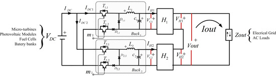
2. Operation Principle of Proposed Converter

The main objective of this proposal is the generation of two isolated DC sources, named VC1 and VC2, from a single power supply VDC, without use of transformers. These isolated DC sources are required for the proper performance of 9-levels DC/AC cascaded cells topology.
To achieve this goal, this paper proposes a modification in the structure of conventional DC/DC Buck Converter, without changes in the operating principle.
The proposed modification consists on a time-lapse high impedance generation between each Buck converter and VDC power supply, to achieve the continuous high impedance states between VC1 and VC2 voltages generated by the Buck converters. Using the converter Buck1 shown in Figure 1, the proposed modification is described. It consists on adding a power switch (T1,2) with the task of opening the ground path of the VDC source. The diode D1,2 is connected in series to T1,2. This connection ensures the unidirectional current flow from the collector to the emitter of T1,2.
Figure 1. Single DC nine-level DC/AC hybrid proposed topology.
Energies 08 01273 g001
The power supply, Vin, is the input voltage of the proposed converter. Vin can be a renewable DC source, such as a solar PV array, a low-voltage wind, or a battery bank. It must be noted that the voltage DC source, Vin, must have a value greater than the peak value of the output voltage, Vout. The recommend range is 1.2 × |Vout| < Vin < 1.5 × |Vout|.
The output voltage, Vout, can be connected to low–medium-voltage power grids or to off-grid AC loads. Since the proposed structure does not need a transformer for any conversions, process, or interconnection, it has advantages, such as higher power density, higher efficiency, lower cost and reduction of total harmonic distortion at output.

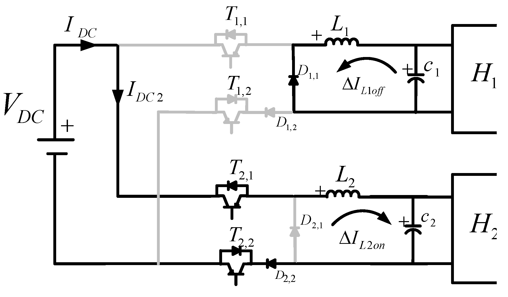
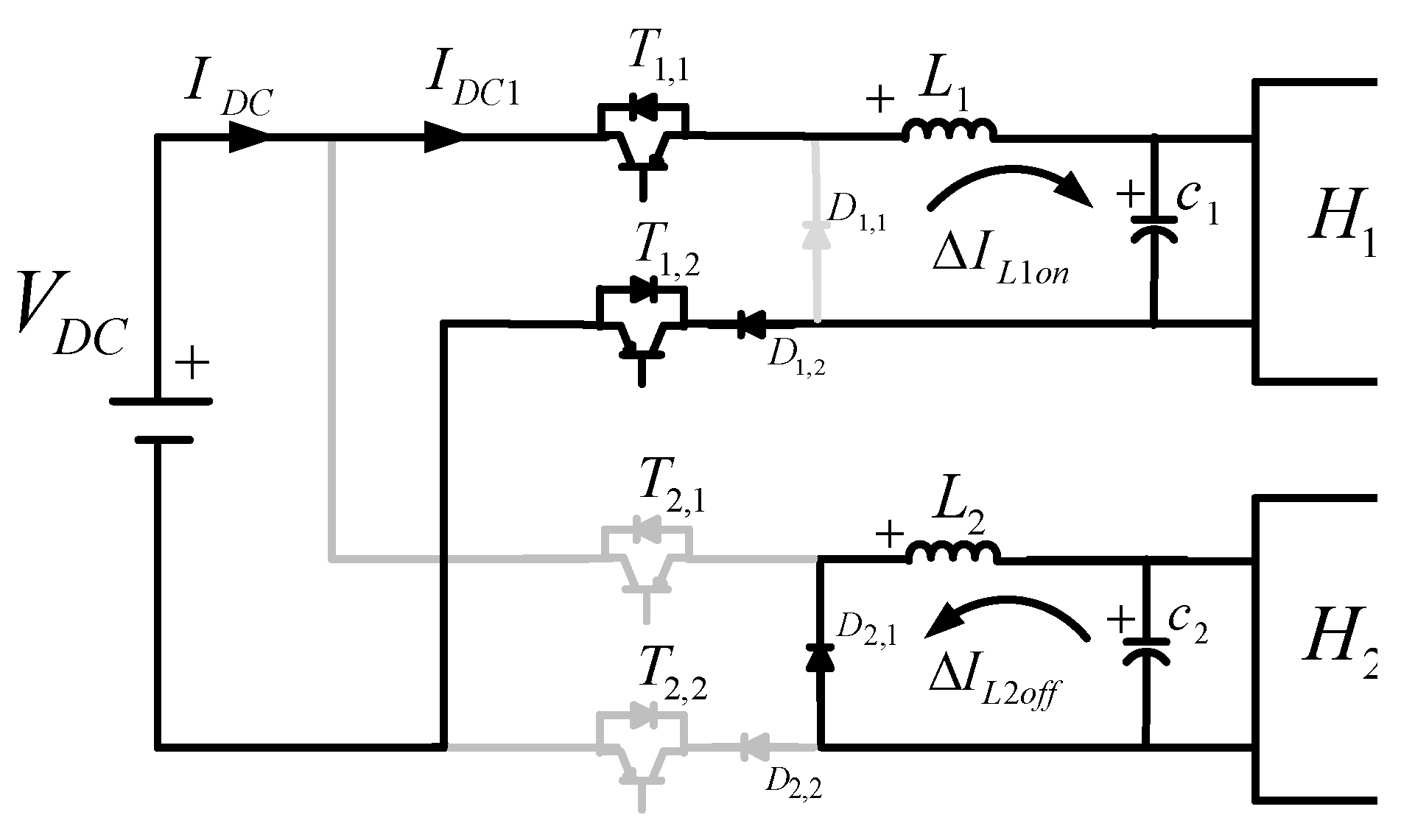
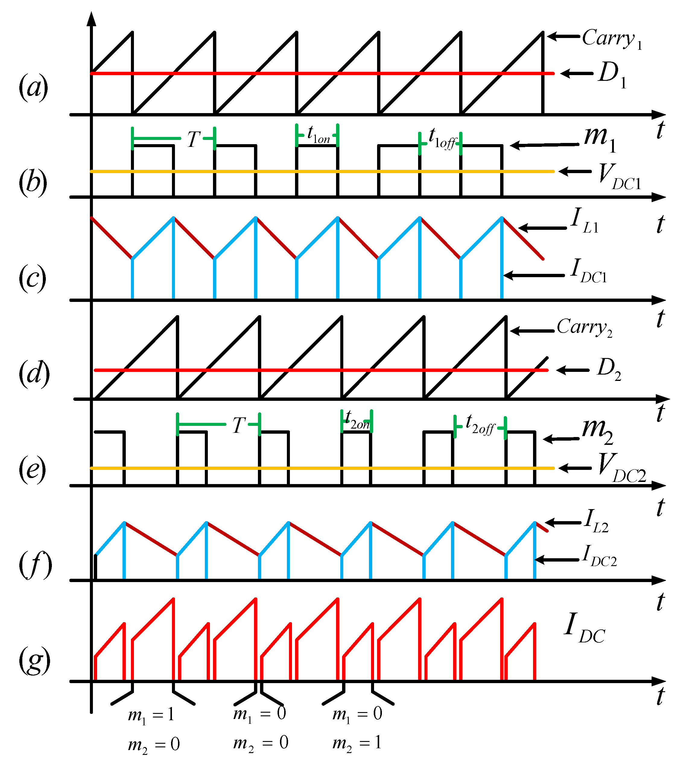
2.1. Isolated Bucks Converters

As shown in the Buck1 converter of Figure 1, the commutation states of the switches T1,1 and T1,2 are controlled in parallel by the control pulse m1, while T2,1 and T2,2 are controlled by m2, on Buck2 converter. The PWM pulses, m1 and m2, are generated based on the magnitude comparison between D1 and D2 modulation signals and carry1, and carry2, ramp signals. The latter signals have a constant 180° phase shift and use the switching frequency, FCBuck. Equations (1)and (2), shown the comparison rules for m1 and m2:
m 1 = { 1 0 w h e n w h e n D 1 > C a r r y 1 D 1 < C a r r y 1
m 2 = { 1 0 w h e n w h e n D 2 > C a r r y 2 D 2 < C a r r y 2
From Equations (1) and (2) it can be deduced a number of topological combinations between Buck2 and Buck1 converters, as shown in Table 2. These states are obtained considering that switching variables m1 and m2 do not take state 1 at the same time instant, which has been termed as a prohibited state for this application.
Table 2. Topological states for buck converters.
Topological Statem1m2IL1IL2ID1,1ID1,2ID2,1ID2,2IDC
(i)00ΔIL1offΔIL2offΔIL1off0ΔIL2off00
(ii)10ΔIL1onΔIL2off0ΔIL1onΔIL2off0ΔIL1on
(iii)01ΔIL1offΔIL2onΔIL2off00ΔIL2onΔIL2on
11Prohibited
Figure 2 and Figure 3 show the main topological states proposed for the Buck converters. Figure 2 shows specifically the topological state (ii) of Table 2, which meets the switching state m1 = 1, and the Buck1 converter takes the ΔIL1on current state, which is dependent on the potential difference between VDC and VC1 as shown in Equation (3):
Δ I L 1 o n = 1 T 0 t 1 o n V D C V C 1 L 1 d t + I L 1 ° = ( V D C V C 1 ) L 1 t 1 o n T + I L 1 °
From Figure 2, it can be deduced that current IDC1 flows from the power supply VDC, from collector-emitter of T1,1 switch, followed by the inductor L1 to the capacitor C1, closing the circuit to ground by D1,2 and the extra switch T1,2. It is noted that for this current mesh, the diode D1,1 is not polarized. Parallel to this process it is noted in Buck2 converter, the current state ΔIL2off, where this current is only dependent of voltage VC1, and initial condition IL2°, as described in Equation (4):
Δ I L 2 o f f = 1 T 0 t 2 o f f V C 2 L 2 d t + I L 2 ° = V C 2 L 2 t 2 o f f T + I L 2 °
In Figure 2, referring to Buck2 converter, it can be seen that the T2,1 and T2,2 switches are in open condition, due to m2 = 0. In this way, a high impedance state is generated between the positive and negative source terminals VDC and the level of voltage VC2, where the current IL2 flows from the positive terminal of the inductance to the cathode of the diode D1,1 to the negative terminal of the capacitor C2.
Figure 2. Topological state (ii), m1 = 1, m2 = 0.
Energies 08 01273 g002
Note that in this commutation state, the VDC power supply is directly connected to the voltage VC1, but in a high impedance state with VC2 voltage. We concluded that there is no direct connection between VC1 and VC2.
Moreover, Figure 3 shows the next commutation stage (iii) of Table 2. It can be seen that the converter Buck1 is in current state ΔIL1off. This current depends only on voltage VC1, and the initial condition IL1°, as described in Equation (5):
Δ I L 1 o f f = 1 T 0 t 1 o f f V C 1 L 1 d t + I L 1 ° = V c 1 L 1 t 1 o f f T + I L 1 °
Parallel to this process, the current IDC2 in the Buck2 converter flows from the power supply VDC to the collector-emitter of T2,1 switch, then to the L2 inductance and afterward toward the capacitor C2, closing the circuit to ground through D2,2 and finally to emitter-collector of switch T2,2:
Δ I L 2 o n = 1 T 0 t 2 o n V D C V C 2 L 2 d t + I L 2 ° = ( V D C V C 2 ) L 2 t 2 o n T + I L 2 °
It is observed that in this trajectory the diode D2,1 is not polarized, so the topological state described (ΔIL2on) is fulfilled by Equation (6).
Figure 3. Topological state (iii), m1 = 1, m2 = 0.
Energies 08 01273 g003
Note that this switching state is complementary to state (ii) in Table 2. The VDC power supply is directly connected to the voltage VC2, but in a state of high impedance is connected to VC1. It can be concluded again, that there is not direct connection between VC1 and VC2.
Finally, the topological state (i), of the switching Table 2, can be considered as a dead time and there is no connection between the power supply VDC with the VC1 and VC2 voltage, where the Buck1 and Buck2 converters acquired a complementary behavior (ΔIL1off and ΔIL2off), as Indicated in the Equations (4)–(6). Figure 4 shows the main waveforms involved in the process of DC/DC conversion, to generate two isolated voltage sources (VC1 and VC2) based on single DC source at input.
The carry1 and carry2 variables are displayed in Figure 4a,d, respectively. In this figure it can be observed 180° of constant phase shift between the control pulses coming from the magnitude comparison between the carry1 and carry2 signals with D1 and D2. The variable modulation technique is shown in Figure 4b,e, in which it can be seen a complementary behavior and a dead time between the rising and falling edges. The generation of control pulses m1 and m2 is based on Equations (1) and (2). These pulses are applied directly to control circuit breakers, being T1,1 and T1,2 controlled by D1 and T2,1 and T2,2 controlled by D2, as previously indicated.
Figure 4. Main waveforms for buck1 and buck2 converters (a) carry1 and D1; (b) m1;(c) IL1 and IDC1; (d) carry2 and D2; (e) m2; (f) IL2 and IDC2; (g) IDC.
Energies 08 01273 g004
Currents IL1 and IL2 in the inductances are shown in red in Figure 4c,f. In these, it can be observed a continuous conduction mode behavior. In the same figure, in blue color, there are shown the waveforms of currents IDC1 and IDC2 generated in each Buck converter, which are dependent of the product of the inductance current and the control drive variable m1 and m2, as is stated in the Equations (7)–(8):
I D C 1 = I L 1 m 1
I D C 2 = I L 2 m 2
Finally, the instantaneous sum of the IDC1 and IDC2 currents is shown through the IDC variable in Figure 4g. This represents the total current supplied by the voltage source VDC, and is calculated by means of Equation (9):
I D C = I D C 1 + I D C 2
The voltages VC1 and VC2 are depending of the inductors currents and the H-Bridges currents, defined as:
V C 1 = ( I L 1 I H 1 ) d t
V C 2 = ( I L 2 I H 2 ) d t
Currents IH1 and IH2 are detailed in the next section. After analyzing the topological states of the Buck converters and by noting the connection and disconnection of alternating VDC voltage source and also by noting a state of continuous high impedance between C1 and C2, we conclude that it is possible to feed the DC/AC multilevel cascaded hybrid cells from a single power supply.

2.2. DC/AC Nine Levels Cascaded Cell Topology
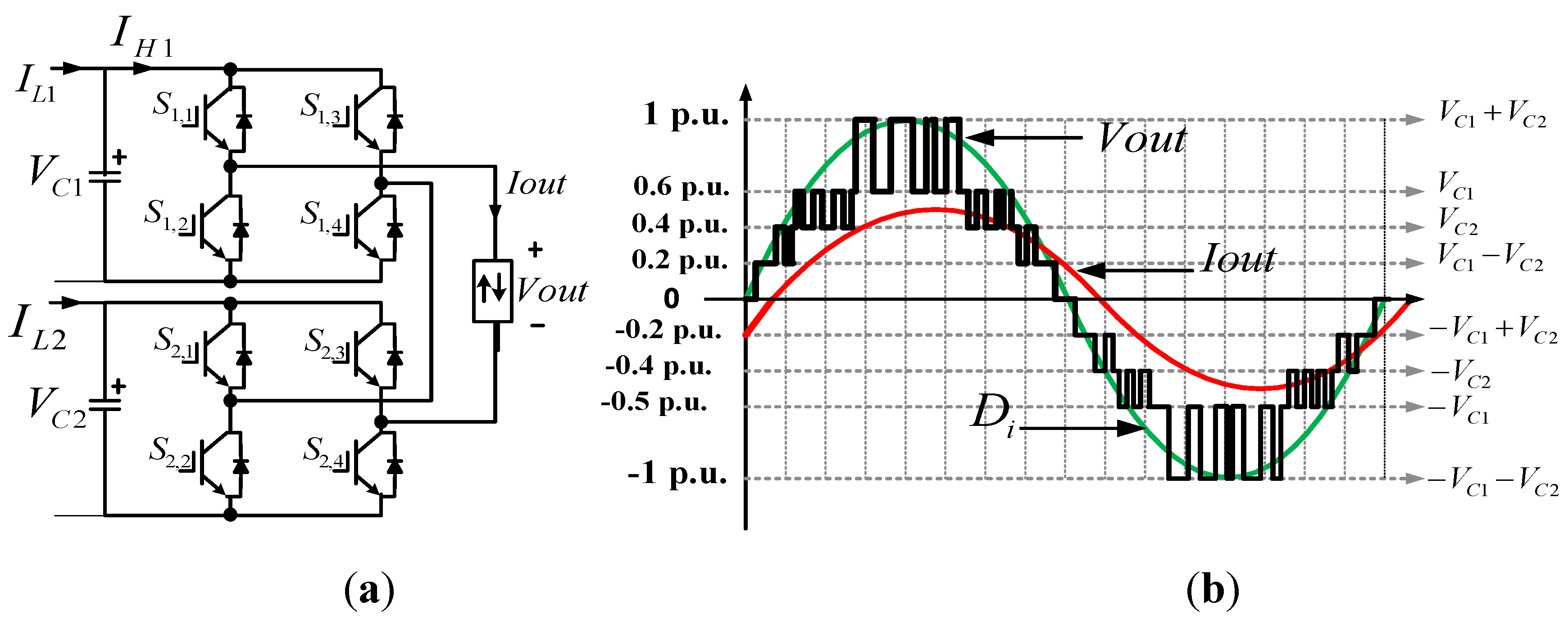
A hybrid, two-bridges, multilevel structure with asymmetrical sources has key advantages over the VSC-NPC and flying capacitor VSC. For instance, it can provide a higher number of voltage levels with fewer switches. In addition, the hybrid topology has no need of capacitors or transformers for its basic operation. As a consequence, using the latter configuration, a sine waveform can be reproduced with lower harmonic distortion than with other multilevel topologies.
The generation of different voltage levels in Vout, from the cascade cell converter, is shown in Figure 5. This voltages are obtained based on the algebraic sum of voltages VC1 and VC2 as shown in Table 3, where H1 and H2 bridges generate combinations independent of voltage versus time, being VH1 є {+VC1, 0, −VC1}; and VH2, є {+VC2, 0, −VC2}; respectively.
Figure 5. Nine levels DC/AC cascaded hybrid converter (a) topology; (b) Vout waveform.
Energies 08 01273 g005
Table 3. Switching states and respective voltage levels.
Vout LevelH1H2
S1,1S1,2S1,3S1,4S2,1S2,2S2,3S2,4
VC1 + VC210011001
VC110011010
VC210101001
VC1VC210010110
010101010
VC1 + VC201101001
VC210100110
VC101101010
VC1VC201100110
Finally, the magnitude and phase shift of Iout depend on the type of load connected to converter, which can be an independent load or a distribution electrical grid. The voltages of each H-bridge converter (VH1 and VH2) can be defined by Equations (12) and (13) as:
V H 1 = V C 1 [ S 1 , 1 S 1 , 3 ]
V H 2 = V C 2 [ S 2 , 1 S 2 , 3 ]
The currents of each H-bridge converter (IH1 and IH2) can be defined by Equations (14) and (15) as:
I H 1 = I o u t [ S 1 , 1 S 1 , 3 ]
I H 2 = I o u t [ S 2 , 1 S 2 , 3 ]
Figure 5 shows the nine levels DC/AC cascaded hybrid topology implemented in this research. It should be mentioned that for the topology employed specifically here, the voltage levels VC1 and VC2 have to satisfy the following ratio:
V C 1 = 3 2 V C 2
where VC1VinD1 and VC2VinD2. Based on Equation (16) it is possible to calculate the duty cycle D1 and D2, applied in Buck1 and Buck2 converters, respectively. It is noteworthy to mention that if the voltage ratio between VC1 and VC2 is different from that stated in Equation (16), then Vout results with deformations and, as a pertinent consequence, some harmonics can be injected to the power grid. The harmonic distortion due to the imbalance of DC sources in DC/AC cascade-cell converter has been already studied [18]. As VC1 and VC2 depend of D1 and D2, a larger or shorter of the latter will deform Vout. The generation of voltage levels Vout is performed based on switching states in Table 3. To obtain the correct control pulses to be applied to inverter power switches connected in cascade is necessary to implement a multilevel modulation Sine-Pulse Width Modulation (SPWM) process, discussed in next section.

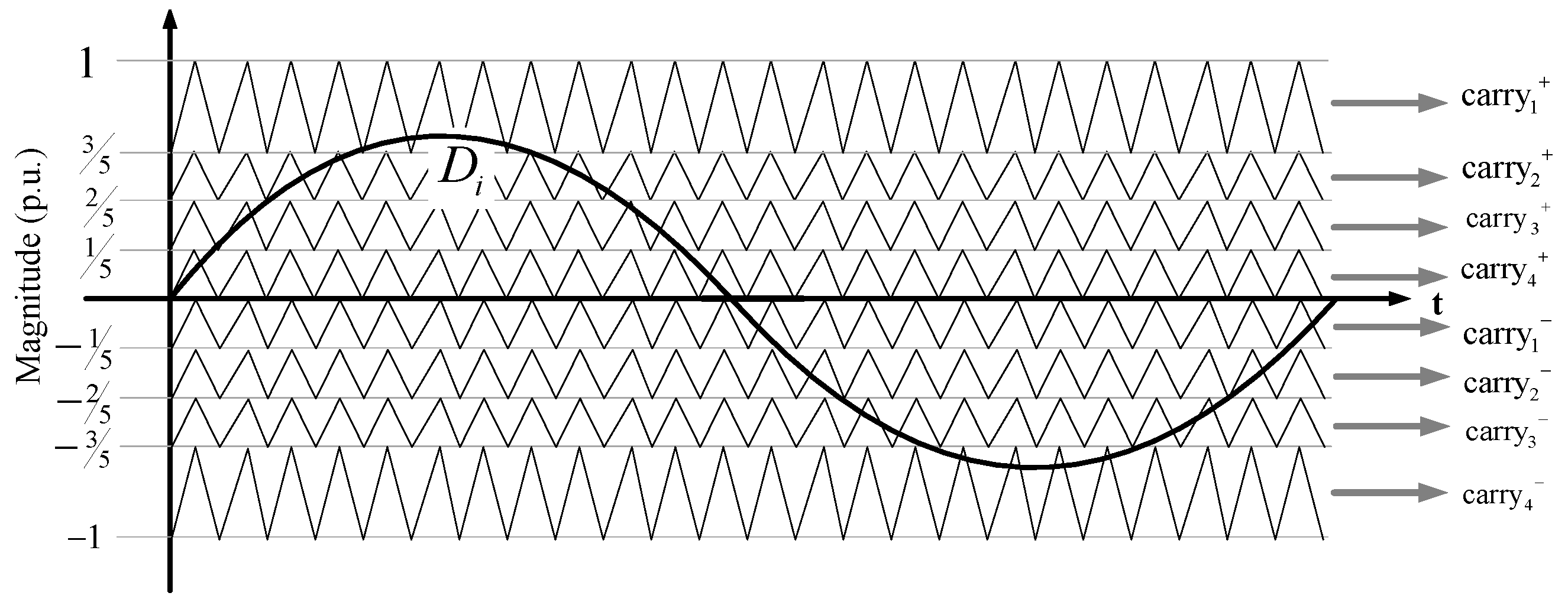
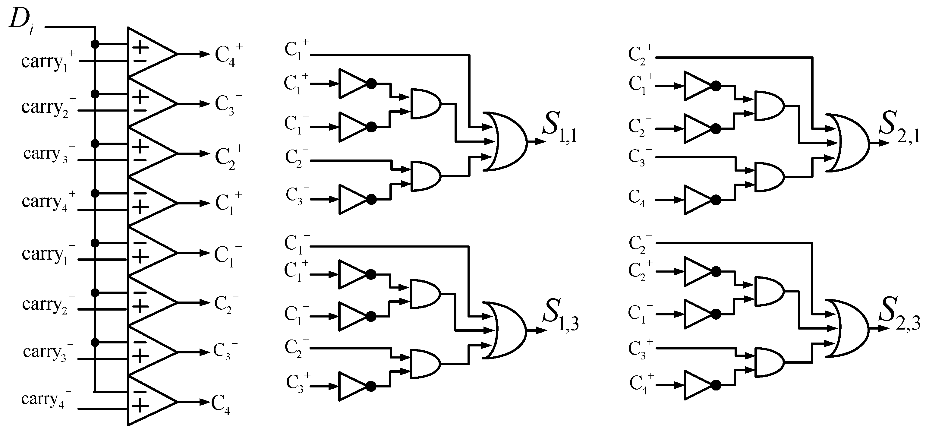
2.3. Nine-Level SPWM Modulation
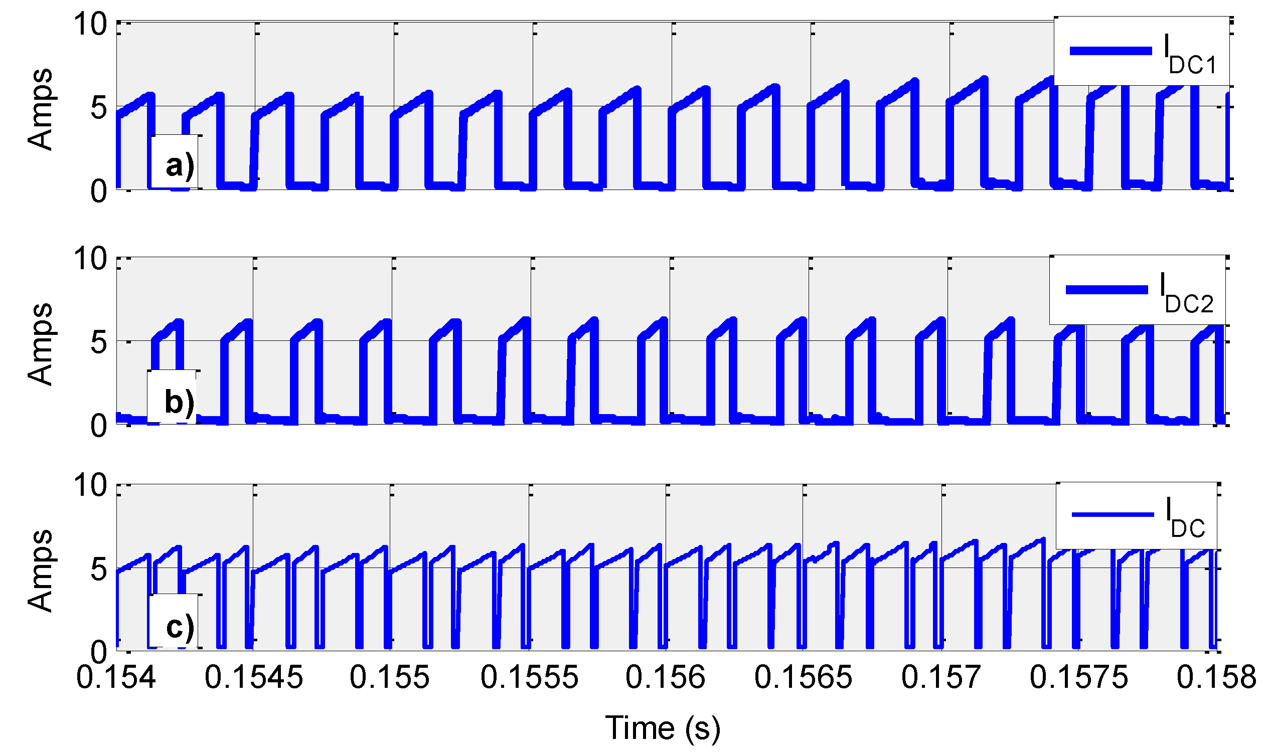
The multilevel modulation process employed for the topology, and shown in Figure 6, is obtained from a magnitude comparison between eight modulating waves carryj and carry+j where j є (1,2,3,4) and a sine modulating signal Di.
Figure 6. Nine levels SPWM scheme.
Energies 08 01273 g006
The control pulses are described by Equations (17) and (18):
C i + = { 1 0 w h e n w h e n c a r r y i + < D i c a r r y i + > D i
C i = { 1 0 w h e n w h e n c a r r y i > D i c a r r y i < D i
In order to obtain the necessary topological stages, described by Table 3, the combinational logic stage is necessary to obtain the required pulses for the cascaded multilevel converter. The logical diagram implemented is shown in the Figure 7.
Figure 7. Combinational logic for IGBT pulses, on cascaded cell topology.
Energies 08 01273 g007
In order to verify the full operation of the converter stages, the Buck converters and the cascaded cells with their respective modulations, a number of simulations have been developed, which are presented in the next section.

3. Simulation

The proposed converter is analyzed through the Simulink—Matlab simulation platform, showing the main variables of voltage, current and control pulses involved in the conversion process of DC/DC through the Buck converters and DC/AC through hybrid cascaded cell converter.
Figure 8a,c shows the switching states of converters Buck1 and Buck2. The alternating duty cycles m1 and m2 ensures the effect of instant isolation between VC1 and VC2. IL1 and IL2 current waveforms are shown in Figure 8b,d, respectively. The behavior of these variables has been verified on the basis of Equations (3)–(6).
Figure 8. IL1 and IL2 currents for buck converters.
Energies 08 01273 g008
The waveforms of currents IDC1 and IDC2, generated by each Buck converter, are shown in Figure 10a,b, respectively. Here, are clear again the alternating switching times between each converter.
Finally the total current IDC supplied by the voltage source VDC, is shown in Figure 9c, which is dependent on the instantaneous sum of IDC1 and IDC2, fulfilling Equation (9).
Figure 9. Current waveforms (a) IDC1, (b) IDC2, and (c) IDC.
Energies 08 01273 g009
The steady-state output voltage of the Buck converters, VC1 and VC2, are shown in Figure 10a. In this figure the relative voltage for proper operation of the hybrid cascaded cell converter is observed, as indicated by Equation (16).
The voltage waveforms generated by the H-Bridge converters, VH1 and VH2, are shown in Figure 10b,c, respectively. From this, it can be seen the topological combinations versus time dependent modulation process, meeting the switching states, Table 2.
Finally, the stepped voltage waveform Vout, is shown by Figure 10d. Vout depends on the algebraic sum of the instantaneous VH1 and VH2 voltages.
Figure 10. Main voltage waveforms (a) VDC, VC1, and VC2; (b) VH1; (c) VH2; and (d) Vout.
Energies 08 01273 g010
Based on the performed simulations it is possible to verify compliance of the main goal of this research: to achieve nine voltage levels DC/AC from a single power supply with only 12 power switches and without transformers.
Additionally, it has been shown by means of circuit simulations that the waveforms satisfy the main equations obtained for the electrical conversion process.

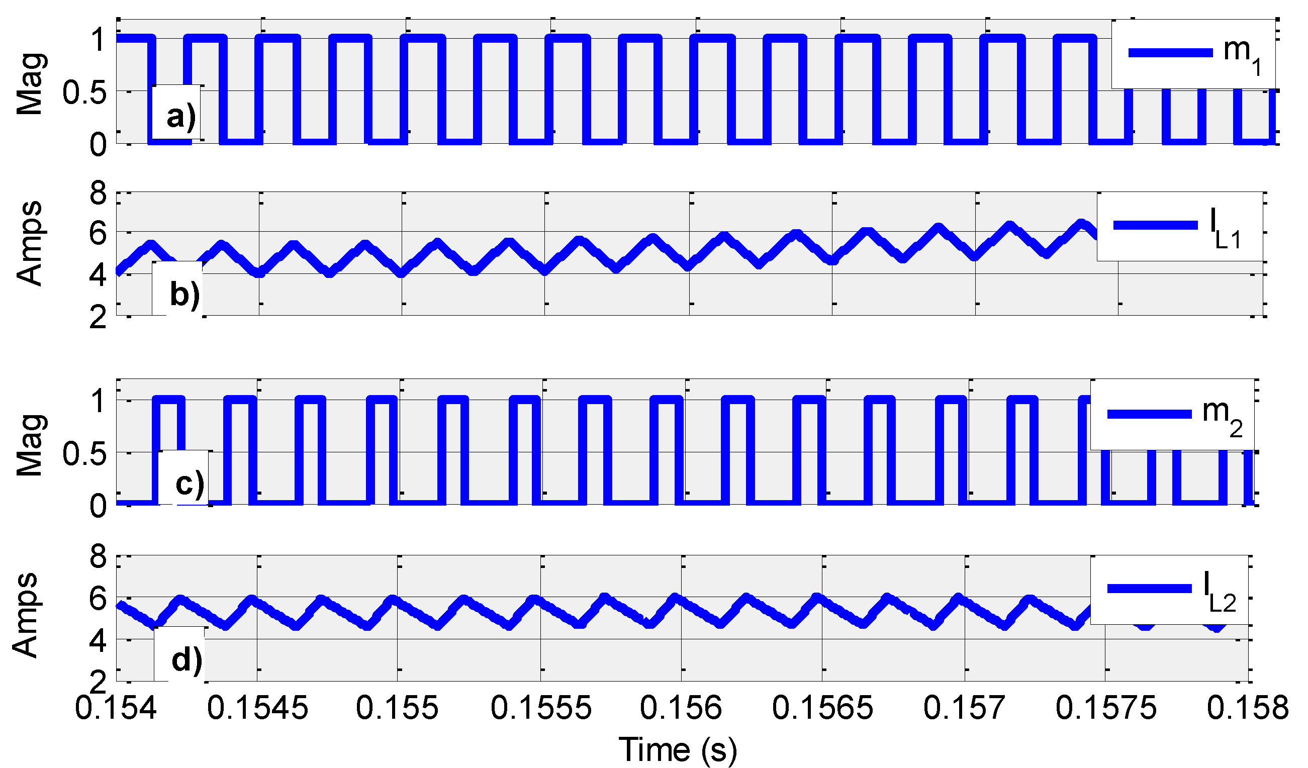
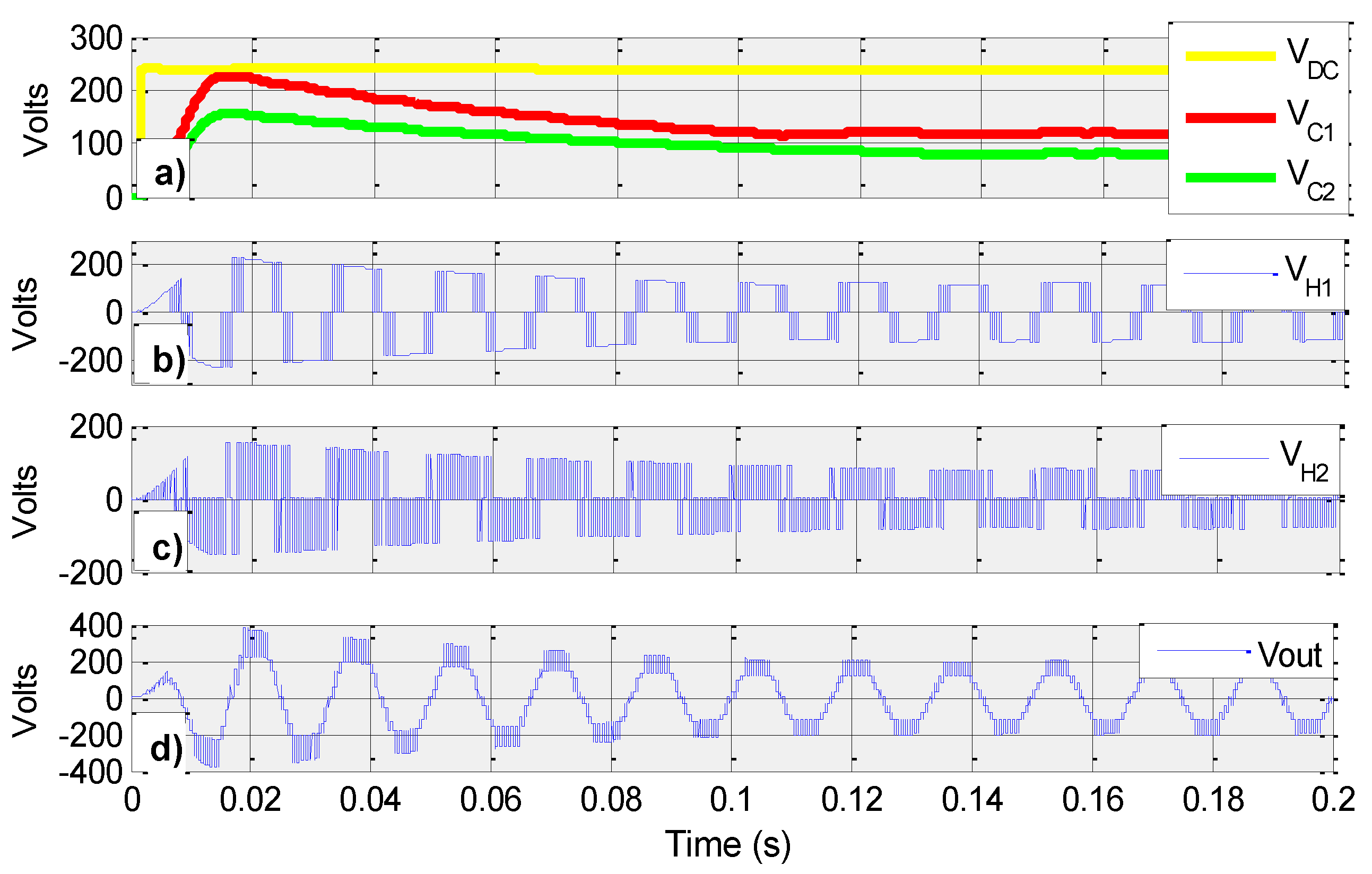
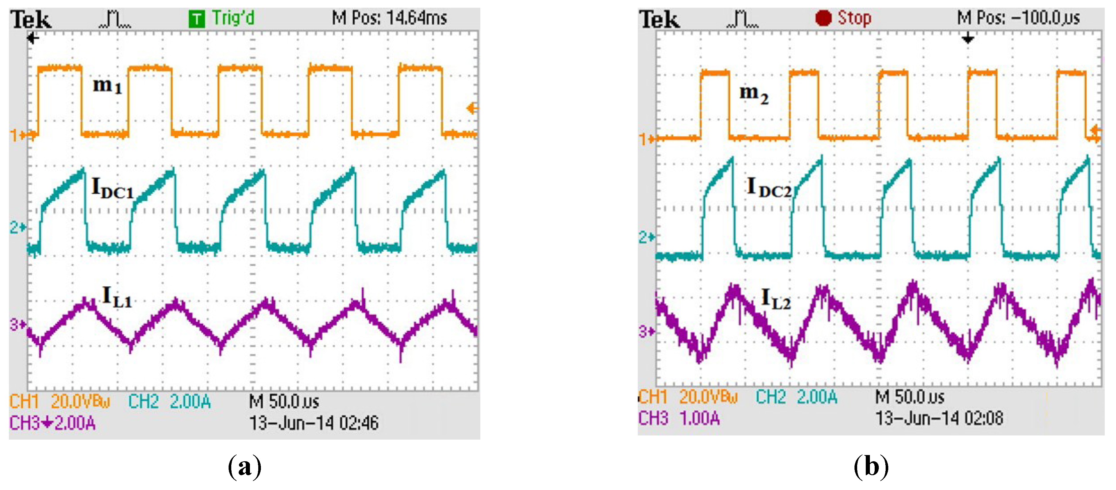
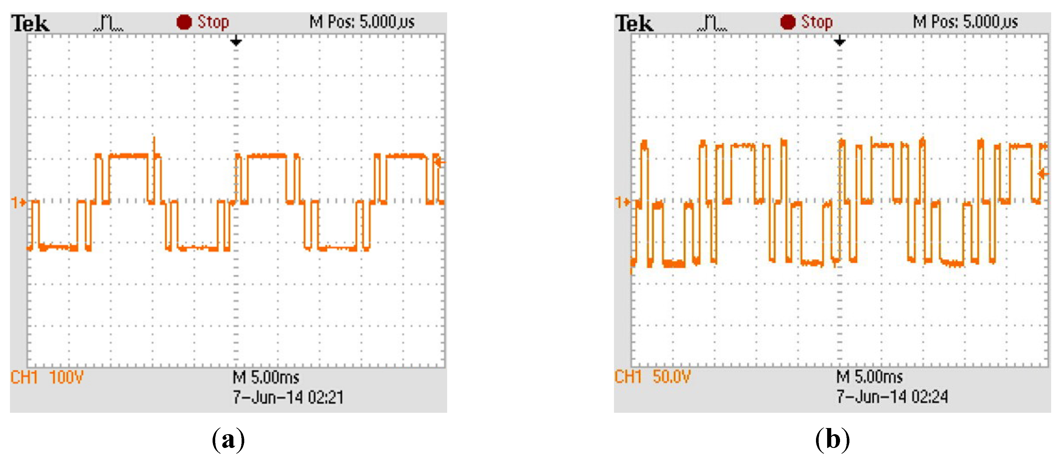
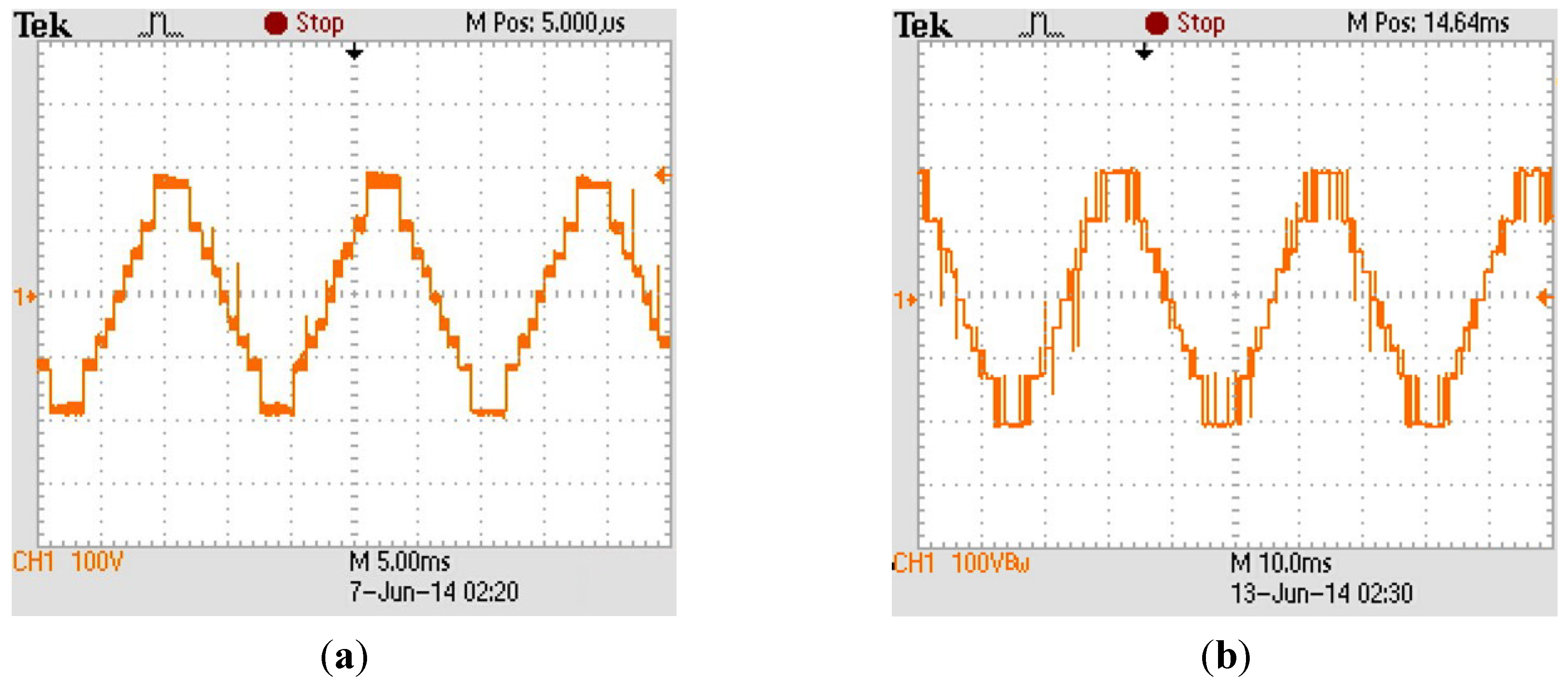
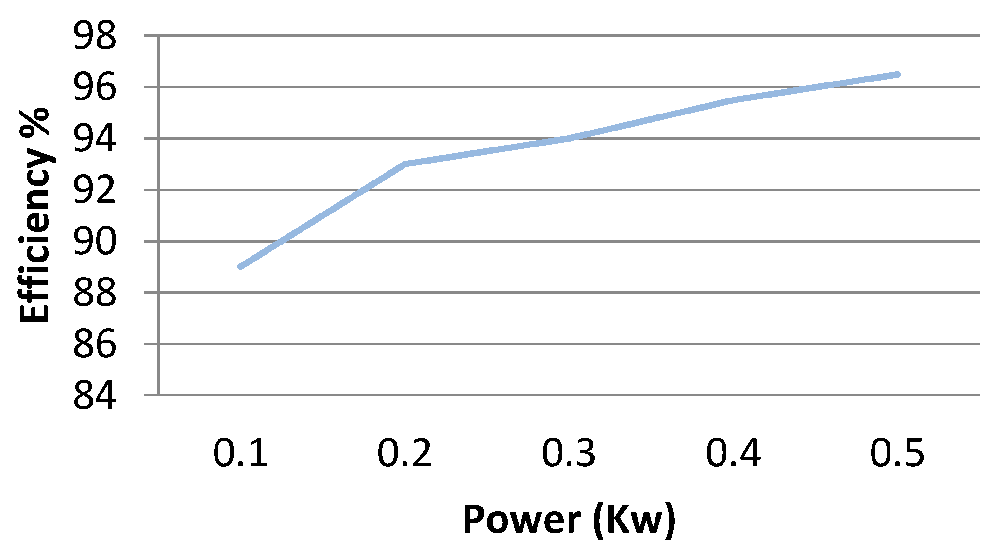
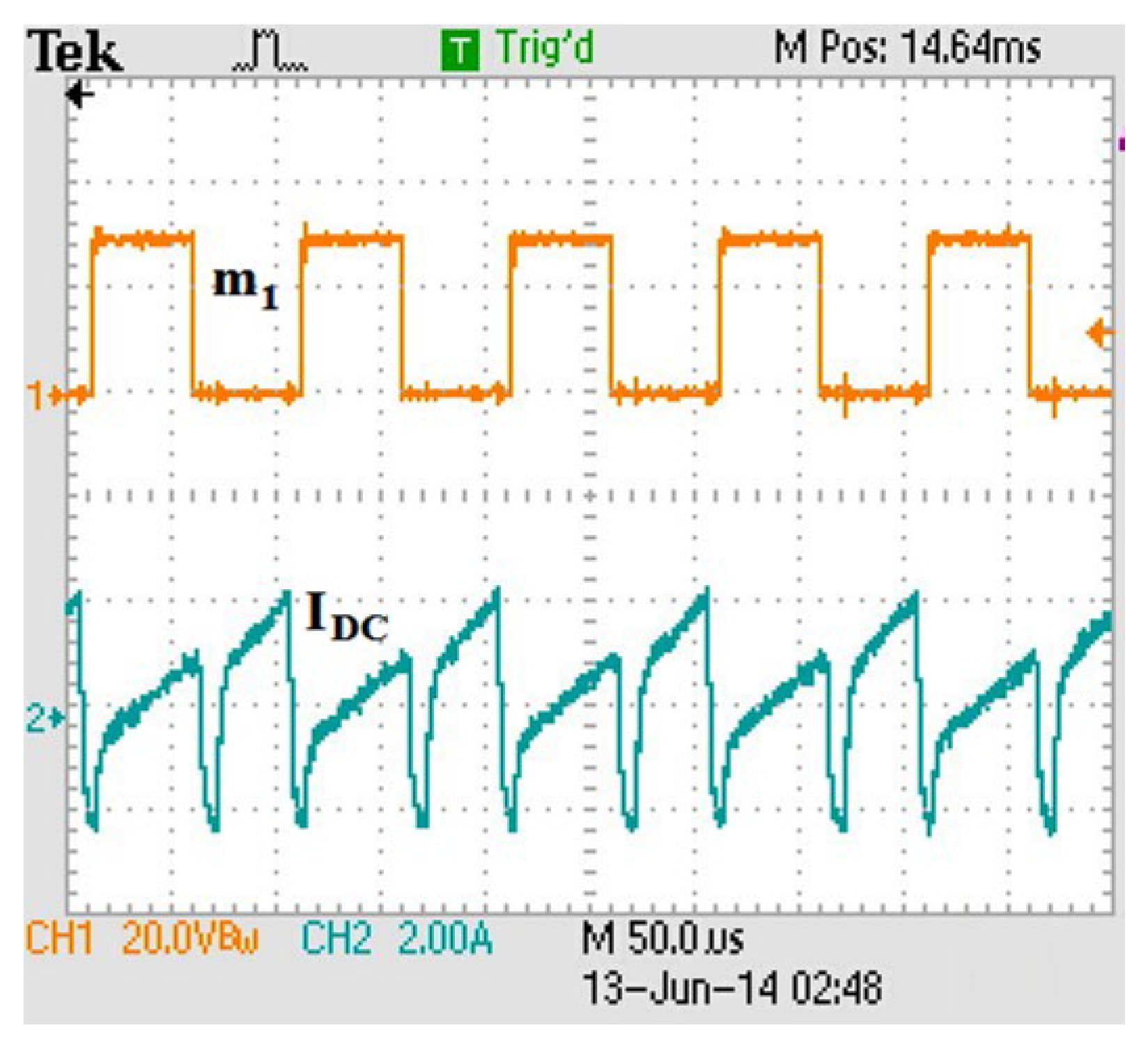
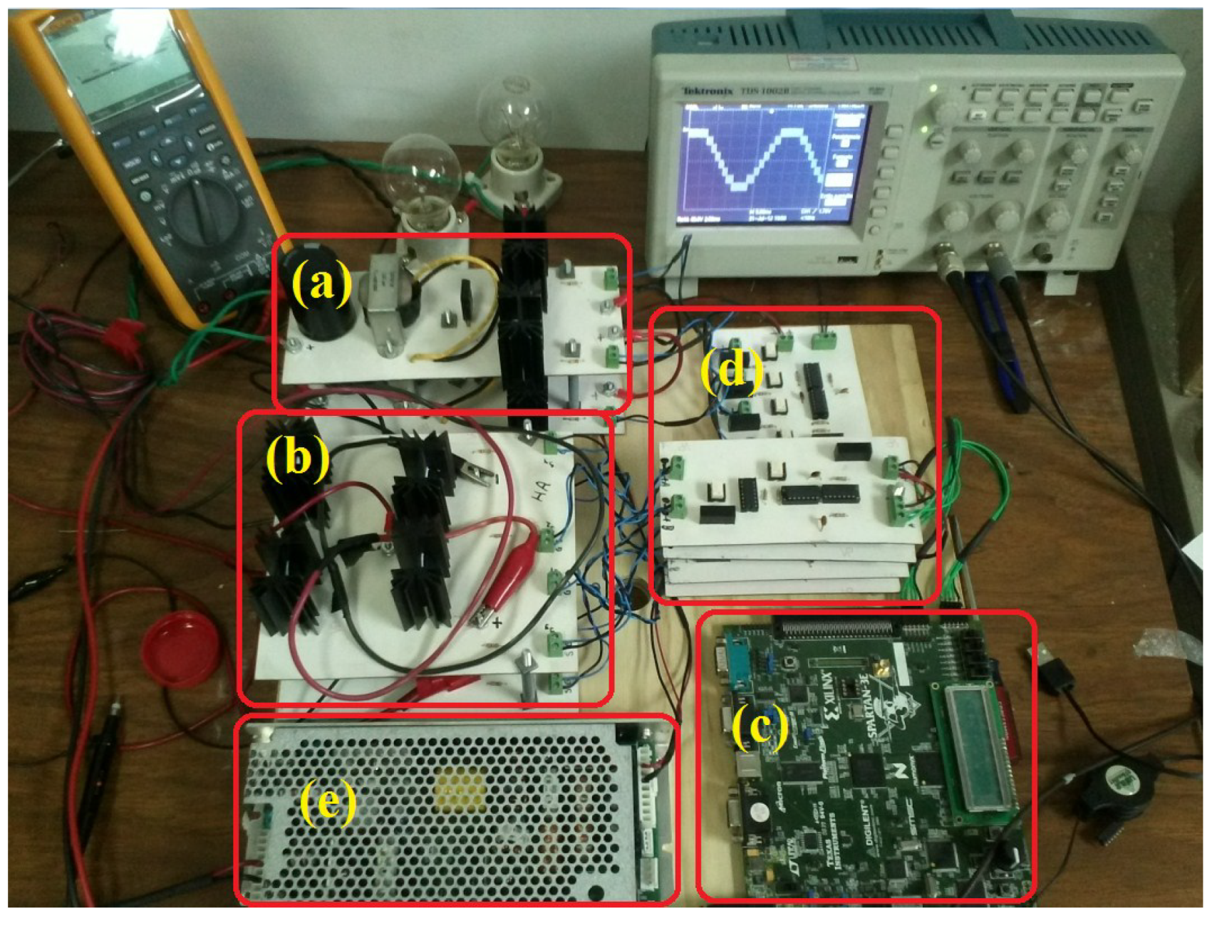
4. Experimental Test

In order to experimentally verify the topology presented, a laboratory prototype has been built using the parameters shown in Table 4. These parameters are the same used in the simulations.In Figure 11a,b can be corroborated experimentally the modulation process of Buck1 and Buck2 converters, respectively, showing the variables modulation m1 and m2, compared to current inductance IL1 and IL2, ending with the currents supplied by the source IDC1 and IDC2.
Table 4. Parameter values for the simulation of the proposed converter.
Variable, ElementValue
Bucks Switching Frequency16 kHz
Multilevel Modulation Frequency6 kHz
L1= L26 mH
C1 = C22200 uF
VDC240 V
D10.5
D20.33
Di0.95∗sin(ωt)
Figure 11. Principal waveforms of the buck converters, (a) m1, IL1 and IDC1 for buck1 and (b) m2, IL2 and IDC2 for buck2.
Energies 08 01273 g011
Under the same case study, Figure 12 shows current IDC, which corresponds to the sum of the currents IDC1 and IDC2 with respect to the control pulse m1.
From these waveforms is possible to corroborate the different switching states of Buck1 and Buck2 converters, shown in Table 2 and analyzed with Equations (7)–(9). Finally, it can be observed that the waveforms exposed in Figure 12 are similar to those shown in Figure 4.
Figure 12. IDC and m1 waveforms.
Energies 08 01273 g012
Under the principle of operation exposed previously, corresponding to the cascaded converter modulation, Figure 13a,b show the experimental voltages generated by each H bridge converter, where it can be seen that VH1 є {+VC1, 0, −VC1}; and VH2 є {+VC2, 0, −VC2}, respectively.
Figure 13. Independent H-bridge voltages (a) VH1; (b) VH2.
Energies 08 01273 g013
Based on the voltages shown by Figure 13a,b, it is possible to corroborate the voltages ratio between VC1 and VC2 as 1:1.5, as stated in Equation (16). The algebraic sum of the VH1 and VH2, corresponding to the output voltage Vout, is shown by Figure 14, where Figure 14a shows an experimental validation of the staggered signal and Figure 14b shows the same output signal with SPWM modulation applied.
Figure 14. Vout (a) multilevel Vout (b) SPWM multilevel Vout.
Energies 08 01273 g014
The multilevel output voltage Vout needs filtering to reduce THD and bring the signal closer to the ideal sinusoidal waveform. As the frequency spectrum of the 3 and 5-level converter is wider than that of the nine-level, the filtering requirements of the latter are less demanding.
Figure 15 presents the scaled-down physical prototype of the nine levels converter with FPGA-based control, the principal auxiliary subsystems and the experimental setup, respectively. Figure 16 shows the efficiency curves against power, obtained from the prototype.
Figure 15. Laboratory prototype of the converter and experimental testing (a) Modified DC/DC buck converters; (b) H-bridges converters; (c) FPGA based control; (d) Drivers pulses for IGBTs; and (e) DC source circuitry.
Energies 08 01273 g015
Figure 16. Efficiency tests.
Energies 08 01273 g016

Discussion

Table 5 shows a comparative analysis between basic DC/AC topologies and the proposed one. It should be remarked that the proposed topology is designed for unidirectional power flow applications only. Nevertheless, Table 5 also shows that the proposed topology has various relative advantages such as fewer power switches, diodes and capacitors compared to structures such as the clamped diode or the flying capacitor. Comparatively to the cascaded-cells topology, this novel nine-levels converter is lesser complex to build because it uses just one power source at input instead of two.
Table 5. Comparative analysis for nine levels DC/AC multilevel converters.
Multilevel ConverterNo. IGBTsNo. CapacitorsNo. DiodesNo. DC Sources
Proposed Topology12261
Clamped Diode168321
Flying Capacitor163201
Cascaded cells8002
A general advantage of the new nine-levels converter over the other configurations is its relative simple control algorithm, without the need of a transformer. These enhanced features make the nine-levels converter introduced in this paper very suitable to application in micro-grids.
The solutions and capabilities presented can be further enhanced. Additional future advances from this work focus on: (i) Minimizing the voltage and current harmonic distortion by means of a suitable modulation scheme; (ii) Obtaining a mathematical model of the dynamic behavior of the nine-level converter and its interaction with distribution grids and a microgrids; (iii) Evaluating the benefits of using various types of LC and LCL filter for the interconnection of the nine-level converter with the grid; (iv) Incorporating the converter to the Smart Grid concept; (v) Analyzing the transient behavior of the converter; and (vi) Evaluate the benefits and limitations of using various types of LC and LCL filter, located in between Vin and the Bucks converters, as a way for obtaining a continuous input current IDC.

5. Conclusions

This work presents a new CD-CA nine-level topology, which combines a modified DC/DC Buck Converter and hybrid Cascade converter based on two H-bridge, in a single phase structure. The most important advantages of the proposed nine-level topology are: (i) Single DC source without need of transformer and (ii) Reduction of power switches.
This topology is a competitive option suitable for an efficient integration and controlling of renewable power sources (such as PV, fuel cells and low-voltage wind generator) into low and medium voltage power grids and microgrids. For instance, a household application is the interconnection of PV modules, while in isolated microgrids the applications may be PV and fuel cells. In other contexts, an ambitious goal is to explore the application possibilities related to the integration of large photovoltaic installations.
This work is a step forward in the direction of reducing the number of elements in a converter structure while improving overall efficiency and enhancing performance relative to other well-known converter configurations.
The authors expect that the step-up multi-level converter introduced in this paper will become a useful alternative for research and development in the area of DC/AC multilevel converters.

Acknowledgments

The authors would like to thank to the TNM (Tecnologico Nacional de Mexico) for the financial support to this project.

Author Contributions

All authors contributed equally to this work. J.R. Rodriguez-Rodríguez performed prototype experiments; Vicente Venegas-Rebollar wrote the manuscript; Edgar L. Moreno-Goytia gave technical support and conceptual advice; and all authors collected and analyzed the obtained data.

Conflicts of Interest

The authors declare no conflict of interest.

References

  1. Arango, E.; Ramos-Paja, C.A.; Calvente, J.; Giral, R.; Serna, S. Asymmetrical interleaved DC/DC switching converters for photovoltaic and fuel cell applications—Part 1: Circuit generation, analysis and design. Energies 2012, 5, 4590–4623. [Google Scholar] [CrossRef]
  2. Rodriguez, J.; Lai, J.S.; Peng, F.Z. Multilevel inverters: A survey of topologies, controls, and applications. IEEE Trans. Ind. Electron. 2002, 49, 724–738. [Google Scholar] [CrossRef]
  3. Tolbert, L.M.; Peng, F.Z. Multilevel converters as a utility interface for renewable energy systems. In Proceedings of the Power Engineering Society Summer Meeting, Seattle, WA, USA, 16–20 July 2000; pp. 1271–1274.
  4. Walker, G.R.; Sernia, P.C. Cascaded DC–DC converter connection of photovoltaic modules. In Proceedings of the 33rd Annual Power Electronics Specialists Conference, Cairns, Queensland, Australia, 22–27 June 2002; pp. 24–29.
  5. Gonzalez, R.; Gubia, E.; Lopez, J.; Marroyo, L. Transformerless single-phase multilevel-based photovoltaic inverter. IEEE Trans. Ind. Electron. 2008, 55, 2694–2702. [Google Scholar] [CrossRef]
  6. Buticchi, G.; Barater, D.; Lorenzani, E.; Concari, C.; Franceschini, G. A nine-level grid-connected converter topology for single-phase transformerless PV systems. IEEE Trans. Ind. Electron. 2014, 61, 3951–3960. [Google Scholar] [CrossRef]
  7. Tsunoda, A.; Hinago, Y.; Koizumi, H. Level- and phase-shifted PWM for seven-level switched-capacitor inverter using series/parallel conversion. IEEE Trans. Ind. Electron. 2014, 61, 1411–1421. [Google Scholar] [CrossRef]
  8. Wu, J.C.; Chou, C. A solar power generation system with a seven-level inverter. IEEE Trans. Power Electron. 2014, 29, 3454–3452. [Google Scholar] [CrossRef]
  9. Sepahvand, H.; Liao, J.; Ferdowsi, M.; Corzine, K.A. Capacitor voltage regulation in single-DC-source cascaded H-bridge multilevel converters using phase-shift modulation. IEEE Trans. Ind. Electron. 2013, 9, 3619–3626. [Google Scholar] [CrossRef]
  10. Roshankumar, P.; Rajeevan, P.P.; Mathew, K.; Gopakumar, K.; Leon, J.I.; Franquelo, L.G. A five-level inverter topology with single-DC supply by cascading a flying capacitor inverter and an H-bridge. IEEE Tran. Power Electron. 2012, 27, 3505–3512. [Google Scholar] [CrossRef]
  11. Rahim, N.A.; Chaniago, K.; Selvaraj, J. Single-phase seven-level grid-connected inverter for photovoltaic system. IEEE Trans. Ind. Electron. 2011, 58, 2435–2443. [Google Scholar] [CrossRef]
  12. Nami, A.; Zare, F.; Ghosh, A.; Blaabjerg, F. A hybrid cascade converter topology with series-connected symmetrical and asymmetrical diode-clamped H-bridge cells. IEEE Trans. Power Electron. 2011, 26, 51–65. [Google Scholar] [CrossRef] [Green Version]
  13. Vazquez, S.; Leon, J.I.; Franquelo, L.G.; Padilla, J.J.; Carrasco, J.M. DC-voltage-ratio control strategy for multilevel cascaded converters fed with a single DC source. IEEE Trans. Ind. Electron. 2009, 56, 2513–2521. [Google Scholar] [CrossRef]
  14. Du, Z.; Tolbert, L.M.; Ozpineci, B.; Chiasson, J.N. Fundamental frequency switching strategies of a seven-level hybrid cascaded H-bridge multilevel inverter. IEEE Trans. Power Electron. 2009, 24, 25–33. [Google Scholar] [CrossRef]
  15. Song, S.G.; Kang, F.S.; Park, S.J. Cascaded multilevel inverter employing three-phase transformers and single DC input. IEEE Trans. Ind. Electron. 2009, 56, 2005–2014. [Google Scholar] [CrossRef]
  16. Ruiz-Caballero, D.A.; Ramos-Astudillo, R.M.; Mussa, S.A.; Heldwein, M.L. Symmetrical hybrid multilevel DC–AC converters with reduced number of insulated DC supplies. IEEE Trans. Ind. Electron. 2010, 57, 2307–2314. [Google Scholar] [CrossRef]
  17. Liu, J.; Cheng, K.; Ye, Y. A cascaded multilevel inverter based on switched-capacitor for high-frequency AC power distribution system. IEEE Trans. Power Electron. 2014, 29, 4219–4230. [Google Scholar] [CrossRef]
  18. Jimenez, O.L.; Vargas, R.A.; Aguayo, J.; Arau, J.E.; Vela, G.; Claudio, A. THD in cascade multilevel inverter symmetric and asymmetric. In Proceedings of the IEEE, Electronics, Robotics and Automotive Mechanics Conference (CERMA), Cuernavaca, Morelos, Mexico, 15–18 November 2011; pp. 289–295.

