Abstract
Variable switching frequency modulation (VSFM) is an easy-to-implement and low-cost method to reduce electromagnetic interference (EMI) of power electronics, yet changes in loss and harmonic behavior make it hard to decide the parameters of the filter and the switching frequency (SF) variation range. In this article, a new VSFM method characterized by evenly distributed SF is proposed, and it is easy to implement. In order to handle the induced variation in loss and current total harmonic distortion (THD) behavior, current dynamics of a full-bridge grid-tied inverter under constant SF modulation (CSFM) are analyzed through multidimensional Fourier decomposition (MFD), and then the results are extended to VSFM. Based on these dynamics, loss of MOSFETs and THD of grid-connected current are estimated through the trapezoidal integral rule, and the analytical expressions of these indexes can be derived. After this, parameters needed for VSFM can be determined while meeting the minimum MOSFET loss and fixed current THD constraint. The performance of EMI, loss, and current harmonic is revealed through simulations and experiments and compared with the CSFM and classical VSFM methods.
1. Introduction
As renewable energy experiences tremendous growth globally, grid-tied inverters, which act as a medium of energy conversion among power generation, transformation, and consumption, are widely distributed in the power system [1,2]. However, these inverters transmit higher and higher noise through power lines because of switching devices driven by a high-frequency pulse width modulation (PWM) signal, which pollutes the electromagnetic environment and threatens the regular operation of devices in the system. Such a situation will not be improved since the tendency of higher power density promotes the application of wide band gap devices like silicon carbide (SiC) MOSFET, which works at an even higher SF. Therefore, reducing the EMI of high-frequency power electronics is essential and necessary [3,4,5].
Generally, EMI standards impose limits on the noise level of industrial equipment within the conducted (150 kHz–30 MHz) and radiated (30 MHz–1 GHz) emission frequency range. However, power electronics are sites where current and voltage fluctuate the most because of their switching characteristic [6]. Parasitic parameters of passive components and shells provide a low impedance path for high-frequency noises [7], and these noises can extend their influence through the power line, as shown in Figure 1a.
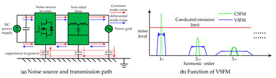
Figure 1.
Noise transmission of power electronics and function of VSFM.
Several typical approaches can effectively reduce the noise level of power electronics, such as an EMI filter, grounding, shielding, and so on. These methods either require additional hardware or modification of original circuits, which might influence the heat dissipation or volume of the original devices [8,9,10,11].
When using CSFM, the inverter’s harmonics are concentrated in mfc ± nf0, where fc is the carrier frequency and f0 is the fundamental frequency. As n gets bigger, the sideband noise soon decreases. As a result, the noise of CSFM concentrates in narrow bands centered in mfc, and the noise spikes are high, as shown in Figure 1b. VSFM reduces EMI noise through time-varying SF and thus expands the spectrum (SS) from a narrow band to a wider range [12], as Figure 1b shows. In this case, harmonics are concentrated in mfc ± nf0 ± kfv, where fv is the frequency of the SF function, and noise spikes are lower and wider compared with CSFM because of energy conservation. Although the noise attenuation effect of VSFM cannot compare with other approaches mentioned before, the method can be realized by simply adjusting the controller of the equipment without changing the original circuits or adding devices. As a result, VSFM is a perfect method for further EMI optimization when the hardware of the device is difficult to modify.
In general, there are four ways to realize VSFM: programmed PWM, random PWM, hysteresis PWM, and periodic PWM (PPWM). Programmed PWM changes the frequency or duty of the PWM signal for specific index minimization, like THD or switching loss [13,14]. In this case, EMI reduction is not the main purpose, and thus, its SS effect is limited. Random PWM changes the frequency or duty of PWM randomly to realize evenly distributed noise within each harmonic band. However, the SS effect achieves the best only when random numbers are generated properly, which means it requires a complex algorithm or additional circuit [15,16]. Hysteresis control changes driving signals once the controlled target crosses the required band, so the controller must act immediately once the target exceeds the limit, which requires a low control cycle or combination with extra devices. Furthermore, since the switching frequency used in hysteresis control depends on the actual feedback signal, protection for the switching process is necessary. PPWM changes SF according to a fixed periodic SS function. This technique is easy to realize and achieves sufficient SS effect and therefore arouses more and more researchers’ interest.
PPWM was originally used for EMI reduction in communication and microprocessor systems [17] and was introduced to the power electronic industry in the 1990s [18]. A number of researchers have made some improvements for specific index optimization or topologies. Conventionally, three functions were used for SS—triangular, sinusoidal, and exponential function [19]—the spectra of which were analyzed through Bessel and Fourier decomposition in [20]; the combination of those functions for minimum noise peak was studied, yet this method only considers voltage noise peak minimization rather than noise peak and ignores its impact on loss and THD characteristics, which means it can only be used when SF varies in a small range. Nowadays, PPWM has developed into three types according to their purposes [6]. The first type is designed for switching loss optimization [21,22]. In this case, the current dynamic of switching devices regarding SF is studied, and SF is determined for the realization of a zero-voltage or zero-current switch. This type of PPWM can decrease switching loss effectively. However, in high-load-current conditions, the inductance must be designed quite small, as a result of which, conduction loss of switching devices and hysteresis loss of core will increase, and the quality of its output current cannot be guaranteed. The second type of PPWM is designed for better voltage/current control. For example, in [23], the bus voltage ripple of the inverter is predicted through a real-time model, and SF is designed for ripple attenuation. Even though this method receives sound ripple attenuation, it ignores the influence of VSFM on the AC side. The third type is designed for EMI reduction; in [24], the author studies the relationship between the SS function and the distribution characteristic of SF and solves the SF function with regard to evenly distributed SF. Although evenly distributed SF does not mean evenly distributed EMI noise, this method shows a better EMI emission reduction effect. In [25], SF functions obeying other typical distribution characteristics were derived, and their loss, harmonic, and EMI performances were compared. However, both [24,25] only provide SF function for specific distribution characteristics, while some fundamental indexes like the loss and THD of grid-connected current are not analyzed, and how to determine parameters of SF are not mentioned, which reduces the practicality of these methods.
Obtaining the relationship between SF function and some fundamental indexes is essential since it offers a guideline for SF parameter determination. Driven by this demand, studies on SF function for loss optimization and THD constraint are conducted. In [26,27], the author determined the switching loss and THD model of a grid-tied full-bridge inverter filtered by a single inductor and then derived the SF function for switching loss optimization. In [28], inductor loss was also taken into account, and the SF function is derived for efficiency optimization (Eff-opt) through the Lagrange Multiplier Method. However, both [26,28] assumed that the SF function was unconstrained to simplify the derivation process and set the part beyond MOSFET’s capability of function to a fixed maximum frequency, resulting in frequency concentration, and a single L filter is not recommended nowadays. In [29], a confined band (CB) VSFM method is designed to minimize the number of pulses and decrease the pulse number when the load current increases. However, switching loss depends not only on current magnitude but also on current direction. Even though the method reduces switching loss and current THD, how the parameters required for VSFM are determined is not clear.
Driven by typical shortcomings of studies in PPWM mentioned above, this article focuses on the SF function that has a better EMI reduction feature, and its parameter selection depends on the loss of MOSFET optimization of a full-bridge grid-tied inverter. Furthermore, the SF function is restricted to guarantee that THD is constant. MOSFET is more temperature-sensitive, and its radiator seriously affects the power density of the inverter compared with the inductor, so this new SS technique can contribute to both EMI and thermal performance improvement, especially for SiC equipment.
The proposed method, using an arithmetic sequence for even frequency distribution, has a better EMI reduction feature compared with the most commonly applied VSFM method using a triangular wave. It is easy to implement since it only requires constant carrier frequency variation, and this feature makes it independent from the current phase and uses fewer computing resources, even when compared with VSFM using a triangular wave. While parameters are decided for loss of switching device optimization, current THD is also taken into consideration in case it exceeds the relevant limit.
This paper is organized as follows: In Section 2, the topology is introduced, and the SF function design method for evenly distributed SF is explained. In Section 3, the current dynamics of inverters are analyzed, and then the MOSFETs’ loss and current THD are derived. In Section 4, the parameter-obtaining scheme of the SF function for loss optimization is explained. The EMI and thermal effects of the VSFM method are validated and compared with CSFM and the typical VSFM method through simulation results in Section 5 and experiment results in Section 6. Finally, conclusions are drawn in Section 7.
2. Topology and SS Method
The topology of the research object is a full-bridge LCL grid-tied inverter, as shown in Figure 2. The voltage of the front-end equipment output after stabilization is considered as an ideal DC voltage source, udc. S1 ~ S4 are SiC MOSFETs. L1, L2, and C1 are inductors and capacitors of a classical LCL filter. To avoid mutual conversion of common-mode and differential-mode EMI noise, L1 and L2 are divided into two equal parts to make the structure symmetric. A power grid is considered as an AC voltage source ug.
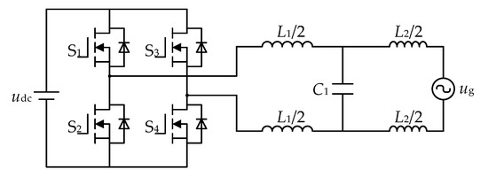
Figure 2.
Topology of single-phase grid-connected inverter.
Generally, the driving signal of an inverter is generated through unipolar frequency doubling modulation or bipolar modulation. The unipolar method uses twice the equivalent SF compared with the bipolar method, so it is more popular in practice. However, to make the analysis process transparent, the subsequent analysis will use the bipolar method as an example, and the case of the unipolar method can be analyzed similarly. The process of bipolar modulation signal generation can be explained by Figure 3. Normally, the power factor of the inverter is set to 1 when there is no specific purpose, so the current reference ig* should be in phase with ug. The phase of grid voltage is obtained through a phase-lock loop (PLL), and ig* is generated by combining the phase and output power requirement; then, the grid-connected current is sampled, and its closed-loop control is executed in the controller. Finally, the modulation wave um comes out of the closed-loop, and then it is compared with a high-frequency triangular carrier wave. D1 is the driving signal of S1 and S4; it is set to 1 when um > uc and 0 in the opposite case. D2 is the driving signal of S2 and S3, which is complementary to D1. Because of high-frequency application, the impedance of L1 and L2 is relatively small at the fundamental frequency. An LCL filter acts as a single inductor equal to L1 + L2 when the frequency is much less than its resonance frequency, which means that whatever the power factor is, the fundamental wave of the inverter’s output voltage is close to ug. This is a useful inference for later analysis.
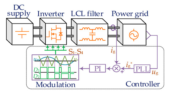
Figure 3.
Process of modulation signal generation.
Even distribution of EMI noise is difficult to realize since it depends not only on the voltage harmonics of the inverter but also on the impedance of the actual circuit. As a result, this paper proposes a more straightforward SF function that undergoes evenly distributed SF. Because of symmetry, the period of the SF function can be half of the fundamental wave’s period T. The SF function is a continuous function, but SF is a discrete sequence in actuality. When considering the kth frequency of the sequence as fk, making { fk } become an arithmetic sequence can directly realize the uniform distribution of SF, which means that fk should obey Equation (1), where fk+1 is the SF after fk, and Δf is the difference between two adjacent frequencies. Furthermore, the sequence { fk } should meet the requirements of Equation (2) since the summary of these switching periods is a quarter of the fundamental period, and K is the number of pulses in this stage. The second half of the SF sequence is symmetrical to the first one, which means that fk+1 = fk − Δf. Equation (1) can be used for VSFM implementation in a digital controller, which is easy and takes little time, but its SF function with respect to t should be solved for loss and THD analysis.
According to the general formula of an arithmetic sequence, fk can be expressed by Equation (3) as a function of k, and Equation (2) can be equivalent to Equation (4), where K is the total switching period in T/4.
When transforming Equation (4) into Equation (5), since K is a large number, 1/K can be considered much less than 1. Once the SF function is determined, K, f1, and Δf are constant, so each item in Equation (5) can be considered as a function value with respect to k/K. The left side of Equation (5) can be determined using the right rectangle formula to achieve numerical integration of function g (τ), where g (τ) is shown as Equation (6) and τ ≈ k/K.
Solving Equation (6), the relationship between K and T/4 can be obtained, as Equation (7) shows. Similarly, the relationship between k and t can be derived as Equation (8).
Combining Equations (3) and (8), the time-domain expression of the SF function f (t) can be obtained as Equation (9). What should be emphasized is that Equation (9) is used for later analysis, and in a real controller, the modulation process can be realized according to Equation (1).
The period of f (t) should be half of the fundamental period. The first half of the SF function is f (t), and the second half is symmetrical to the first part. Distributions of SFs when using Equation (9) and using a triangular wave within the same range are shown in Figure 4. Obviously, the number of switching periods of the proposed method in each interval with equal length is almost unchanged, while that of the triangular wave increases as SF increases. When the frequency variation range is expanded, the non-uniform distribution of SFs becomes more severe. Such a phenomenon is easy to determine: a high-frequency switching period takes less time, so when the time intervals are equal, the interval where the value of the SF function is higher generates more switching periods. As a result, the SF function should be abrupt when the value is large enough to cross the high-frequency region quickly and slowly in the opposite case, but the slope of the triangular wave remains unchanged during the whole process, and a frequency concentration will unavoidably appear.
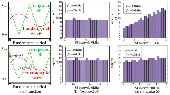
Figure 4.
SF distribution of proposed function and triangular wave.
In general, the proposed SF function using an arithmetic sequence performs a perfectly uniform distribution of SFs compared with the typical triangular SF function, and it is easy to implement, even when compared with the triangular SF function, since it only requires a constant increase in SF. This advantage will occur especially when the frequency variation range is expanded.
3. Current Dynamics Analysis
The proposed SF function only determines how SF changes over time, but its variables are still undecided. In this section, these variables are determined for switching loss and conduction loss optimization since MOSFETs are more sensitive to temperature and their radiators occupy a greater space. Furthermore, whichever one the SF function is, the THD of the grid-connected current must be restricted. As a result, it is essential to study the current dynamics of both the grid side and the inverter side.
3.1. Current Dynamic of Inverter Side
The current on the inverter side directly decides switching loss and conduction. Because the voltage fluctuation of C1 is much less than that of the inverter output and the impedance of L2 is quite small at the fundamental frequency, it is reasonable to assume that the voltage of C1 is equal to the grid voltage. As a result, the structure of the grid-tied inverter is equivalent to a simplified circuit, as shown in Figure 5, where iL1 is the current of L1 and uAB is the output voltage of the full bridge.
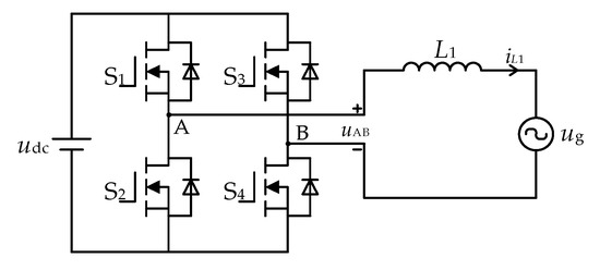
Figure 5.
Simplified circuit for studying inverter current.
To study iL1, the voltage spectrum of uAB should be calculated for preparation. As mentioned in Section 2, the fundamental wave of uAB is in phase with ug, so the time-domain expressions of ug and um are shown in Equation (10), where ω0 is the angular frequency of ug.
When using CSFM, uAB can be expressed as Equation (11), where sign (t) = 1 when t > 0 and sign (t) = −1 when t < 0; uc (t) is a triangular wave ranging from −1 to 1 and its cycle is 2π; and ωc and φc are the angular frequency and phase of the carrier wave.
When considering the free variables of the angle of modulation wave and carrier wave, like y = ω0t and x = ωc + φc, then uAB will be a binary function with respect to x and y. The new function uAB (x,y) is a periodic function about both x and y, and the period is 2π, the surface of which is shown in Figure 6. As has been shown, in a single period, the shape of the function is a cylinder, and its boundary is the intersection points of um (y) and the rising and falling edges of uc (x), as shown in Figure 6a.
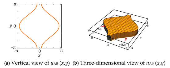
Figure 6.
Shape of uAB (x,y).
Since uAB (x,y) is a binary periodic function, it can be decomposed by a two-dimensional Fourier transform. The result is shown in Equation (12), where Jn represents the nth-order Bessel function, m is the harmonic order, and n is the sideband order. Harmonic order m means the harmonics are centered in m fc, and the sideband order describes how far apart the harmonic and m fc are.
When substituting the time-domain expression of x and y, the spectrum of uAB (t) can be derived.
When combining Equation (13) and the circuit in Figure 5, iL1 can be expressed as Equation (14) when under a stable state.
Directly using Equation (14) to analyze the current dynamic of the inverter side is difficult since it is an infinite series, yet it helps determine some special points to construct the current variation process. At the beginning and end of the switching cycle (ωc t + φc = 0, 2π), when considering two opposite numbers n and –n, according to the parity of Bessel and trigonometric functions, the sum of their corresponding items in Equation (14) is 0 (including n = 0). Likewise, in the middle of the switching cycle (ωc t + φc = π), the same conclusion can be derived. Generally, at the boundary and middle of a switching period, there exists only a fundamental wave. In a single switching period, uC1 can be considered to be maintaining its fundamental value at the middle point tm since its variation is much less than uAB; therefore, iL1 varies linearly, as shown in Figure 7. The mentioned variables are expressed in Equations (15) and (16), where Δt1 is the stage inverter outputs udc and Δt2 is the stage inverter outputs –udc; k1 and k2 are slopes of the current in stages Δt1 and Δt2, respectively; and Tm is the period of the mth switching cycle. At the turning points of iL1, the inverter causes switching action, and the points can be calculated through a linearized current dynamic model.
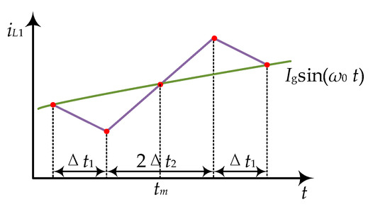
Figure 7.
Current dynamic of inverter side using CSFM.
When combining Equations (15) and (16), the relationship between the current slope and stage can be derived for simplification: k1 = −4udc Δt2/(L1 Tm); k2 = 4 udc Δt1/(L1 Tm). With the two equations, switching points can be calculated.
A transient waveform can be used to calculate switching points and the effective value of iL1, the former of which can be used to estimate switching loss, and the latter can be used to estimate conduction loss.
According to the waveform in Figure 7, the mean square (MS) value of a switching period can be calculated, as shown in Equation (17).
The MS of iL1 can be solved through a rectangular numerical integration method to obtain its parse expression as in Equation (18), the time division of each item can be considered Tm, and the value of the item can be considered as the area of the function inside curly brackets. Since the integral term is a low-frequency part, the accuracy of numerical integration can be guaranteed. The MS of iL1 can be divided into two parts: the first part results from the fundamental wave, and the second part results from switching action.
When it comes to the VSFM case, the angle of the carrier wave will no longer be linear to t. The phase of the carrier wave can be expressed as Equation (19), where f (τ) is the SF function. However, since Equation (12) is determined by absolute angle x rather than t, the current waveform in each switching period can still be described by Figure 7, but Tm is the corresponding period at tm instead of a constant value. Likewise, Tm in Equations (15), (16), and (18) should be replaced by 1/f (tm), and then the turning points and MS value of iL1 for the VSFM case can be derived as well.
3.2. Current Dynamic of Grid Side
The current dynamic of the grid side determines the THD of the grid-tied current, and it can be analyzed through circuit and spectrum characteristics. The transfer function of a typical LCL inverter is expressed in Equation (20).
Generally, SF should be far away from the resonance point of the LCL inverter, so the transfer function of the harmonics resulting from switching action can be simplified as Equation (21), where iL2H is the high-frequency harmonic component of iL2 and uABH is that of uAB.
According to Equation (21), the equivalent impedance decreases 60 dB per decade, so the second-order harmonic or higher and their sidebands can be neglected. Combined with the spectrum of uAB, the transient expression of harmonic components of iL2 for the CSFM case is shown in Equation (22).
Some features of the Bessel function can be utilized to simplify THD calculations. As can be seen, only even sideband harmonics exist in the first sideband. Bessel function curves of Jn (Mπ/2) for M from 0 to 1 are shown in Figure 8. In terms of the first-order harmonic and its sidebands, summation terms in Equation (22) are relatively small when n ≥ 4, so they can be neglected as well.
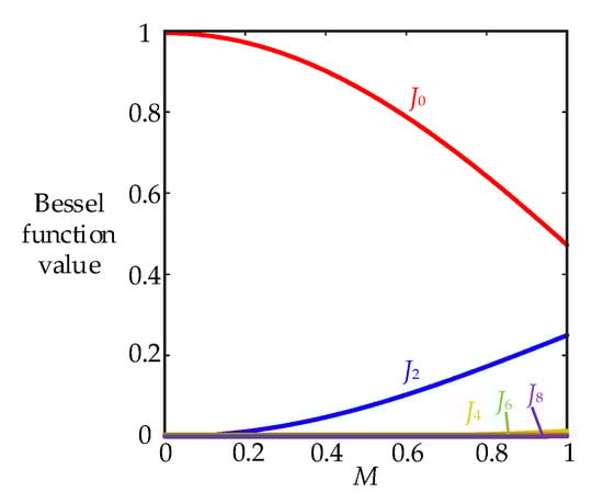
Figure 8.
Bessel function curves Jn (Mπ/2) with respect to M.
In short, the harmonic dynamic of iL1 can be approximated as Equation (23) when the frequency of uc (t) is much greater than that of um (t). Obviously, harmonic current is a product of the low-frequency part relating to the modulation frequency and the high-frequency part relating to the carrier frequency. In a single switching period, the low-frequency part can be considered constant, and thus, it can be assumed to be a sinusoidal signal.
According to Equation (23), the harmonic component of iL2 is 0 at the beginning and end of each switching period, regardless of SF or circuit parameters. As a result, when it comes to VSFM, the harmonic current dynamic can be considered to be the same as CSFM in each switching period, as shown in Equation (24).
When calculating the MS value of iL2H, the low frequency in each period can be considered to be constant. The MS value of iL2H (t) is shown in Equation (25), and consequently, the THD of the grid-connected current can be calculated as well.
4. Parameter Determination of SF Function for Loss Optimization
The designed SF function in Equation (9) has two variables to determine. For simplification, the SF function is expressed as Equation (26).
For loss optimization, the relationship between f (t) and switching loss or conduction loss should be estimated. In terms of switching loss, this depends on the direction of the current. According to Equations (15) and (16), the switching current of the inverter can be calculated as Equation (27). iupper is the current of iL1 at the rising edge of S1’s driving signal and ilower is the opposite.
Based on Equation (27), the upper and lower current contours are revealed in Figure 9a. At upper switching points, S2 and S3 are switched on, while S1 and S4 are switched off. Since the upper contour is always greater than zero, switching loss is generated from the switching off of MOSFETs in S1 and S4 and the switching on of diodes in S2 and S3. In terms of lower switching points, S1 and S3 are switched off, while S1 and S4 are switched on. Before the upper contour crosses the zero-point tc, switching loss is generated from the switching on of diodes in S1 and S4 and the switching off of MOSFETs in S2 and S3, as shown in Figure 9b.
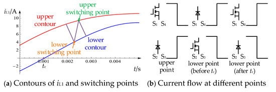
Figure 9.
Switching points and current flow states of inverter.
Whatever the direction of the current, the generated loss is the combination of the turn-on loss of two MOSFETs and the turn-off loss of two diodes, or the opposite case. Since udc is constant, switching loss depends simply on load current once the circuit is determined. The relationship between loss and load current is assumed to be represented by Equation (28), in which qon denotes the loss generated from the switching on of one MOSFET and the switching off of one diode at load current i, and qoff is the opposite; ρon and ρoff are constants.
Switching loss in T/4 can be expressed as Equation (29), where R is the number of switching periods in T/4 and r1 is the number of switching periods before lower switching periods cross zero.
The summation in Equation (29) can be approximated as an analytical solution through a rectangular numerical integral, as shown in Equation (30). It is not the total loss derived from Equation (29) because it ignores the parts irrelevant to SF for simplification.
In terms of conduction loss, current direction can also make a difference, but the harmonic component resulting from the SF function is small, and thus, conduction loss can be considered proportional to the average value of on resistance, Ron, as shown in Equation (31).
In general, the process of seeking SF parameters for MOSFET loss optimization can be regarded as a constrained optimization problem with respect to tc, A, and α, as shown in Equation (32). The first equation constraint results from zero-point tc; the second constraint is a THD restriction. The reason for the first inequality constraint is the distance restriction from the resonance point of the LCL filter, and the second is due to the MOSFET’s capability.
The optimization problem in Equation (33) can be solved by solving the Kuhn–Tucker (KT) points. KT conditions for optimization problem (33) can be expressed in Equation (33), where x is [A α tc]T, and it can be solved through a numerical search algorithm.
For a grid-tied inverter, the DC side voltage is usually stabilized through the front-stage inverter, and the AC side is the grid; both of them can be considered fixed for a certain inverter. However, the inverter’s output current might be changeable according to output power requirements, but Equation (33) cannot be solved in real time in a digital controller. As a result, optimal frequency ranges when ig is set to a series of determined values can be calculated, and other optimal values with respect to different ig values can be estimated through linear interpolation.
The whole control structure can be summarized in Figure 10. The closed-loop control part is the same as the traditional control technique of an inverter. k1 determines the output current magnitude. The current of L2 is sampled for PI control, and that of C1 is sampled for active damping; then, the required modulation wave is generated. Once the current magnitude is determined, the optimal frequency ranges can be calculated through table lookup and interpolation, and then fmax and Δf can be estimated. Since the loss and THD of a single fundamental period are not essential, fmax and Δf are recommended to be updated at the start of the fundamental period when ig* changes. This can not only reduce the number of calculations, but it can also make f (t) independent from PLL. The switching frequency only needs a constant value variation according to the monotonicity of the absolute current value. When combining the calculated frequency and counting cycle of the controller’s PWM module, the counting number that determines the next carrier frequency will be calculated, and the driving signals will be generated.
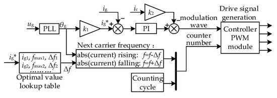
Figure 10.
Control structure of the proposed method.
5. Simulation Verification
A grid-tied inverter is established in CST Studio Suite, and the general structure is shown in Figure 11a. In the simulation platform, the high-frequency characteristics of PCB and other components should be properly demonstrated. As a result, parasitic parameters of the PCB are extracted through the RLC solver, and thus, the spice model of the PCB can be obtained. Passive devices can be simulated through their typical high-frequency model, and their parasitic parameters are simply set to reasonable values since this is not the key point of this paper. MOSFETs are simulated through the spice model provided by their manufacturers. The simplified equivalent circuit and essential parasitic parameters are shown in Figure 11b. The main ground capacitance is generated from the dissipation surface of MOSFETs and the grounded heat sinks, which can be expressed as capacitors between the drain pin and ground.
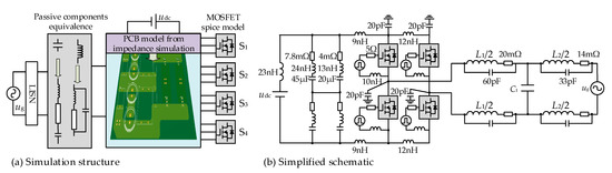
Figure 11.
Grid-tied inverter EMI simulation structure.
Other necessary parameters of the main power circuit are listed in Table 1.

Table 1.
Parameters of inverter for simulation.
Conducted emissions under different ranges are simulated when the inverter uses CSFM (using the middle point of the frequency range), the proposed VSFM, and the typical triangular VSFM. The simulation results are shown in Figure 12. As can be seen in the figure, the conducted noise of both VSFM methods is reduced by around 5 dBμV in most conducted emission frequency ranges. The noise of the proposed method is about 4 dBμV smaller than that of triangular VSFM when the variation range of frequency is large. If the variation range of frequency is within 20 kHz, there is almost no difference between the two VSFM methods, which means that the proposed method performs better (or at least the same) in EMI reduction while using fewer computing resources of the digital controller. Since the inverter is modulated by the bipolar method, which generates little common-mode noise, clearly, VSFM has the greatest effect at low-frequency ranges, where differential-mode noise influences the output the most.
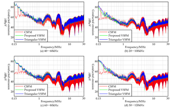
Figure 12.
Conducted emission simulation results.
For loss optimization, the relationship between ρon or ρoff and current can be fitted through the PLECS thermal model provided by the manufacturers. In this paper, the SiC MOSFET SCT4045DE from ROHM Company is used for simulation, and the corresponding ρon and ρoff are 1.103 × 10⁻⁵ (J/A) and 1.267 × 10⁻⁶ (J/A), respectively. Similarly, the on resistance can be derived, which is 63 mΩ. The maximum SF of the device is set to 100 kHz.
The thermal resistance of the contact material and radiator can be obtained through the thermal steady-state solver. The contact material is silicone grease, which is 0.1 mm high, and its area is the same as the MOSFET’s interface. When setting the ambient temperature to 25 °C and considering the chip as a 5 W heat source, a thermal steady-state solver is executed. The simulation result is shown in Figure 13, and the thermal resistance from case to ambient temperature, Rca, can be consequently derived. In this paper, Rca is set to 6.7 K/W.
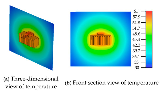
Figure 13.
Simulation result of MOSFET’s temperature.
The thermal simulation circuit in PLECS is set up, and the parameters are the same as those in Table 1. When the grid-tied current is 10 A, the current THD is 5% and the maximum SF is 100 kHz; the searched KT point (A = 47,540 Hz; α = −136.7; tc = 0.0043 s) and plots of MOSFETs’ loss with respect to A and α are shown in Figure 14. As can be seen in the figure, when tc gets bigger, A and α get smaller to decrease the lower current contour. The THD constraint limits SF in a constant cylinder, and the optimal value can be found through the junction between the cylinder and the loss surface. It can be seen that the searched KT point is the global optimal point obeying the THD constraint. The reason for a constant THD restriction instead of maximum THD is that the KT point might move towards where α is relatively small, thus reducing the effect of SS.
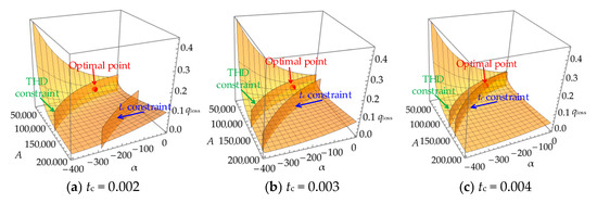
Figure 14.
Loss surface and constraints at different tc values.
The simulated case temperatures and grid-connected currents are shown in Figure 15. The minimum SF is four times the resonant frequency (24 kHz). Because the optimal frequency range is relatively small, where conduction loss influences it the most, temperature rise increases as the SF range increases, and the current THD will be smaller than the reference. When it comes to SF ranges whose THD is the same as the optimal point, their temperature rise is higher, although there exist cases where both the THD and thermal performance of points that do not obey the THD constraint are better than the calculated optimal point. However, when removing the constant THD constraint, the searching algorithm might seek an optimal point that generates the least current distortion, and SFs might concentrate in a narrow high-frequency range, thus reducing their EMI performance, so a constant THD constraint is necessary to avoid that condition.
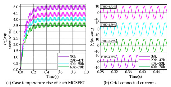
Figure 15.
Thermal and current THD performance of different SF ranges (THD constraint: 5%).
When setting the reference THD as 2%, simulation results of the calculated optimal point (A = 100 kHz; α = −271; tc = 0.0037; fmax = 100 kHz; fmin = 25.4 kHz) and other non-optimal parameters that realize the same THD are determined, as shown in Figure 16. As can be seen from the figure, while meeting the same THD requirement, the temperature rise of the case using the calculated optimal value generates the least loss compared with using its neighborhood points. If the performance of thermal or EMI is not ideal, the value of the THD can be adjusted according to real conditions, and the whole process remains unchanged.
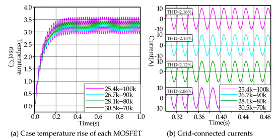
Figure 16.
Thermal and current THD performance of different SF ranges (THD constraint: 2%).
Compared with CB VSFM [29] at the optimal frequency range (25.4 k ~ 100 kHz) for the sake of fairness and Eff-opt VSFM at the optimal frequency range derived by itself (63.7 k ~ 100 kHz), case temperature and current waveforms of the three methods are revealed in Figure 17. The proposed VSFM method shows better MOSFET loss behavior than CB VSFM and Eff-opt VSFM. Eff-opt VSFM in [28] calculated switching loss with the assumption that switching loss is directly proportional to the square of current in each switching period, regardless of current direction, which generates little error for the L-filtered inverter but is not suitable for the LCL-filtered inverter. Furthermore, it should be pointed out that how the frequency range of CB VSFM is determined is not mentioned in [29], but in this article, it is determined by using the optimal range calculated with the previously mentioned method.
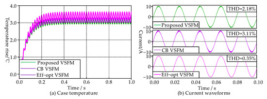
Figure 17.
Case temperature and current waveforms of CB VSFM and the proposed method.
Conducted emission performances of the three methods are shown in Figure 18. The Eff-opt method obtains an optimal SF function via the Lagrange Multiplier Method, considering only the THD constraint, and it sets the part of the SF function beyond the maximum frequency to the maximum frequency, which leads to severe frequency concentration. The proposed VSFM performs the best in terms of conducted emissions because of its evenly distributed SFs, the conducted emission of which is about 5 dBμV smaller than the two other methods.
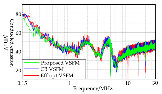
Figure 18.
Conducted emissions of different VSFM methods.
When the reference current drops from 10 A to 5 A, the optimal frequency range is determined by the interpolation curve of the nearest two optimal points. The simulated junction temperatures and current waveforms when using the new estimated optimal frequency range and the original range are compared in Figure 19. If the original frequency range is applied, the loss of MOSFETs is not optimal, and the THD exceeds the preset constraint. When the current varies, the optimal frequency range must change correspondingly to guarantee that THD will not exceed the limit and that the loss of switching devices is optimal under the current condition.
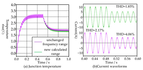
Figure 19.
Loss and harmonic performance of the proposed method when the current changes.
6. Experiment Verification
A full-bridge grid-tied inverter prototype is built for EMI, case temperature, and THD measurement. The experiment results are shown below to prove the effectiveness of the proposed method. Parameters of voltage sources and filters are the same as Table 1.
When the variation range remains the same, the conducted emissions of the inverter when using CSFM, VSFM with a triangular wave, and the proposed method are shown in Figure 20. As can be seen from the experiment results, the proposed method mainly works in the intermediate frequency of the conducted emission band, where the proposed method is generally 3 dB smaller than triangular VSFM and 10 dB smaller than CSFM. However, when the variation range of frequency gets smaller, the difference between VSFM and CSFM is almost negligible in a frequency band less than 1 MHz.
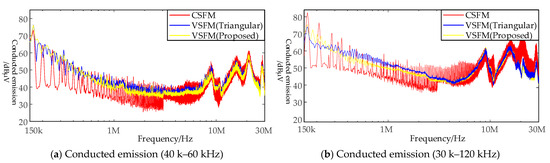
Figure 20.
Comparison of conducted emissions of different methods: (a) 40 kHz to 60 kHz; (b) 30 kHz to 120 kHz.
When comparing the optimal range and its neighborhood in Section 5, when the THD constraint is 2%, the respective grid-connected current waveforms are determined, as shown in Figure 21. THD can be calculated through the measured RMS value. The frequency ranges are supposed to keep the THD as 2%. However, due to the delay of the digital control system and the error of sampling, there exist low-frequency harmonics. Although these harmonics might influence THD estimation and optimal frequency range calculation, we can either leave some margin for THD or consider the harmonics to be constant since they are independent of switching actions.
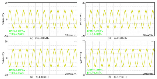
Figure 21.
Grid current waveforms under different frequency ranges when THD is constrained to 2%.
The respective harmonic spectrums of currents in Figure 21 were obtained through FFT, and the results are exhibited below in Figure 22. As can be seen from harmonic curves, the low-frequency harmonics resulting from a non-ideal controller and sampling are almost unaffected by switching frequency, so leaving a constant margin for low-frequency harmonics when estimating THD is reasonable. Furthermore, the harmonic amplitude peak is not necessarily reduced when the variation range of frequency is enlarged, and this phenomenon might be caused by the overlap between different sidebands.
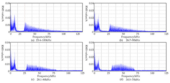
Figure 22.
Grid currents’ harmonics under different frequency ranges when THD is constrained to 2%.
Because the junction temperature cannot be measured directly, the temperature of the back side of the MOSFET is measured to reveal the loss of the MOSFET. Thermal images of the MOSFET when using the four frequency ranges mentioned above are shown in Figure 23, where the ambient temperature is 23 °C. According to these images, it can be seen that the actual temperature is higher than the simulation, which may be because of the non-ideal attachment of dissipation surfaces. The calculated optimal range is found at the lowest temperature, which reveals the effectiveness of the parameter acquisition method for VSFM.
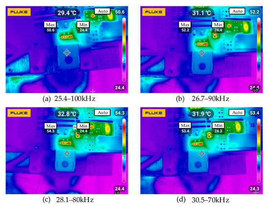
Figure 23.
Thermal images under different frequency ranges when THD is constrained to 2%.
7. Conclusions
In this paper, a new VSFM method considering both EMI and thermal performance is proposed. To begin, SF varies as an exponential function, and a uniform distribution of SF is realized. However, this function is derived from an arithmetic sequence, which means that the period required for the next instance is easy to calculate in the controller, even when compared with the easiest triangular SF function, making it suitable for high-frequency applications. When the variation range of SF is constant, the conducted emission of the proposed method is about 4 dBμV less than that of the triangular SF function.
To increase the practicality of the proposed method, parameter selection based on MOSFETs’ loss optimization is designed. A constant THD constraint is applied to ensure that the algorithm will not seek a loss-optimal point while ignoring the variation range of SF, which could lead to negative EMI performance. Current dynamics of the inverter and the grid side are analyzed to calculate the MOSFET’s loss and current THD while the error is limited within 6%. The optimal point is searched through the KKT method. Simulation and experiment results prove that the searched point is loss-optimal while realizing the same current THD.
Parameter determination of the proposed VSFM method focuses on the loss of switching devices since they are more sensitive to temperature and require a bulky heat sink, and the heat dissipation capacity of inductors is better. However, there exist cases where inductor loss is more influential. Furthermore, a wider noise spectrum makes it easier for the inverter to be resonant with the complex power grid impedance.
Future study will concentrate on the careful consideration of thermal performance and the trade-off between loss of switching devices and inductors to ensure that the selected parameters are the most suitable for various working conditions. The efficiency of the proposed method should be analyzed to better refine its operating region; characteristics of grid impedance must be analyzed, and the harmonic level of VSFM should be reconsidered to avoid possible resonance with the grid; an advanced control scheme concerning active damping might be applied to decrease the risk of resonance.
Author Contributions
Conceptualization, H.L.; VSFM method, W.C.; current dynamic analysis, F.C. and Z.L.; loss analysis, H.L.; optimization, P.W. All authors have read and agreed to the published version of the manuscript.
Funding
This work was supported by the technology cooperation project of State Grid Jiangsu Electric Power Co., Ltd., under Grant J2024200.
Data Availability Statement
The original contributions presented in this study are included in the article. Further inquiries can be directed to the corresponding author.
Conflicts of Interest
Authors Hengmen Liu and Zhong Liu were employed by Yangzhou Power Supply Company of State Grid Jiangsu Electric Power Co., Ltd. Authors Wei Chen and Fang Chen were employed by State Network Yangzhou Jiangdu District Power Supply Company. The remaining authors declare that the research was conducted in the absence of any commercial or financial relationships that could be construed as a potential conflict of interest. The authors declare that this study received funding from State Grid Jiangsu Electric Power Co., Ltd. (grant number J2024200). The funder was not involved in the study design, collection, analysis, interpretation of data, the writing of this article or the decision to submit it for publication.
References
- Wang, Y.-F.; Yang, L.; Wang, C.-S.; Li, W.; Qie, W.; Tu, S.-J. High step-up 3-phase rectifier with fly-back cells and switched capacitors for small-scaled wind generation systems. Energies 2015, 8, 2742–2768. [Google Scholar] [CrossRef]
- Arango, E.; Ramos-Paja, C.A.; Calvente, J.; Giral, R.; Serna, S. Asymmetrical interleaved DC/DC switching converters for photovoltaic and fuel cell applications—Part 1: Circuit generation, analysis and design. Energies 2012, 5, 4590–4623. [Google Scholar] [CrossRef]
- Widek, P.; Alaküla, M. Methods for the Investigation and Mitigation of Conducted Differential-Mode Electromagnetic Interference in Commercial Electrical Vehicles. Energies 2025, 18, 859. [Google Scholar] [CrossRef]
- Wang, K.; Lu, H.; Li, X. High-Frequency Modeling of the High-Voltage Electric Drive System for Conducted EMI Simulation in Electric Vehicles. IEEE Trans. Transp. Electrif. 2023, 9, 2808–2819. [Google Scholar] [CrossRef]
- Lin, J.-Y.; Hsu, Y.-C.; Lin, Y.-D. A Low EMI DC-DC Buck Converter with a Triangular Spread-Spectrum Mechanism. Energies 2020, 13, 856. [Google Scholar] [CrossRef]
- Zhou, L.; Preindl, M. Variable Switching Frequency Techniques for Power Converters: Review and Future Trends. IEEE Trans. Power Electron. 2023, 38, 15603–15619. [Google Scholar] [CrossRef]
- Xiang, Y.; Pei, X.; Zhou, W.; Kang, Y.; Wang, H. A Fast and Precise Method for Modeling EMI Source in Two-Level Three-Phase Converter. IEEE Trans. Power Electron. 2019, 34, 10650–10664. [Google Scholar] [CrossRef]
- Fan, W.; Shi, Y.; Chen, Y. A Method for CM EMI Suppression on PFC Converter Using Lossless Snubber with Chaotic Spread Spectrum. Energies 2023, 16, 3583. [Google Scholar] [CrossRef]
- Zhang, Y.; Li, H.; Shi, Y. Electromagnetic Interference Filter Design for a 100 kW Silicon Carbide Photovoltaic Inverter Without Switching Harmonics Filter. IEEE Trans. Ind. Electron. 2022, 69, 6925–6934. [Google Scholar] [CrossRef]
- Kumar, M.; Kalaiselvi, J. Analysis and Measurement of Non-Intrinsic Differential-Mode Noise in a SiC Inverter Fed Drive and Its Attenuation Using a Passive Sinusoidal Output EMI Filter. IEEE Trans. Energy Convers. 2023, 38, 428–438. [Google Scholar] [CrossRef]
- Hoffmann, S.; Bock, M.; Hoene, E. A New Filter Concept for High Pulse-Frequency 3-Phase AFE Motor Drives. Energies 2021, 14, 2814. [Google Scholar] [CrossRef]
- Li, H.; Liu, Y.; Lü, J.; Zheng, T.; Yu, X. Suppressing EMI in Power Converters via Chaotic SPWM Control Based on Spectrum Analysis Approach. IEEE Trans. Ind. Electron. 2014, 61, 6128–6137. [Google Scholar] [CrossRef]
- Zhao, C.; Costinett, D. GaN-Based Dual-Mode Wireless Power Transfer Using Multi-frequency Programmed Pulse Width Modulation. IEEE Trans. Ind. Electron. 2017, 64, 9165–9176. [Google Scholar] [CrossRef]
- Poon, J.; Johnson, B.; Dhople, S.V.; Rivas-Davila, J. Programmed Pulsewidth Modulated waveforms for Electromagnetic Interference Mitigation in DC-DC converters. IEEE Trans. Power Electron. 2020, 36, 5915–5925. [Google Scholar] [CrossRef]
- Lee, K.; Shen, G.-T.; Yao, W.-T.; Lu, Z.-Y. Performance Characterization of Random Pulse Width Modulation Algorithms in Industrial and Commercial Adjustable-Speed Drives. IEEE Trans. Ind. Appl. 2017, 53, 1078–1087. [Google Scholar] [CrossRef]
- Boudouda, A.; Boudjerda, N.; Drissi, K.E.K.; Kerroum, K. Combined random space vector modulation for a variable speed drive using induction motor. Electr. Eng. 2016, 98, 1–15. [Google Scholar] [CrossRef]
- Gamoudi, R.; Chariag, D.E.; Sbita, L. A Review of Spread-Spectrum-Based PWM Techniques—A Novel Fast Digital Implementation. IEEE Trans. Power Electron. 2018, 33, 10292–10307. [Google Scholar] [CrossRef]
- Poon, J.; Johnson, B.B.; Johnson, S.V.; Sanders, S.R. Minimum Distortion Point Tracking. IEEE Trans. Power Electron. 2020, 35, 11013–11025. [Google Scholar] [CrossRef]
- Balcells, J.; Santolaria, A.; Orlandi, A.; Gonzalez, D.; Gago, J. EMI reduction in switched power converters using frequency Modulation techniques. IEEE Trans. Electromagn. Compat. 2005, 47, 569–576. [Google Scholar] [CrossRef]
- Huang, J.; Xiong, R. Study on Modulating Carrier Frequency Twice in SPWM Single-Phase Inverter. IEEE Trans. Power Electron. 2014, 29, 3384–3392. [Google Scholar] [CrossRef]
- Chen, T.; Yu, R.; Huang, A.Q. Variable-Switching-Frequency Single-Stage Bidirectional GaN AC–DC Converter for the Grid-Tied Battery Energy Storage System. IEEE Trans. Ind. Electron. 2022, 69, 10776–10786. [Google Scholar] [CrossRef]
- Meng, Y.; Sun, J.; Duan, Z.; Jia, F.; Wang, X.; Wang, X. Variable Voltage Variable Frequency Modular Multilevel AC/AC Converter with High-Frequency Harmonics Filtering Capability. IEEE J. Emerg. Sel. Top. Power Electron. 2022, 10, 811–821. [Google Scholar] [CrossRef]
- Li, Q.; Jiang, D. Variable Switching Frequency PWM Strategy of Two-Level Rectifier for DC-Link Voltage Ripple Control. IEEE Trans. Power Electron. 2018, 33, 7193–7202. [Google Scholar] [CrossRef]
- Chen, J.; Jiang, D.; Shen, Z.; Sun, W.; Fang, Z. Uniform Distribution Pulsewidth Modulation Strategy for Three-Phase Converters to Reduce Conducted EMI and Switching Loss. IEEE Trans. Ind. Electron. 2020, 67, 6215–6226. [Google Scholar] [CrossRef]
- Chen, J.; Jiang, D.; Sun, W.; Shen, Z.; Zhang, Y. A Family of Spread-Spectrum Modulation Schemes Based on Distribution Characteristics to Reduce Conducted EMI for Power Electronics Converters. IEEE Trans. Ind. Appl. 2020, 56, 5142–5157. [Google Scholar] [CrossRef]
- Mao, X.; Ayyanar, R.; Krishnamurthy, H.K. Optimal Variable Switching Frequency Scheme for Reducing Switching Loss in Single-Phase Inverters Based on Time-Domain Ripple Analysis. IEEE Trans. Power Electron. 2009, 24, 991–1001. [Google Scholar]
- Xia, Y.; Roy, J.; Ayyanar, R. Optimal variable switching frequency scheme for grid connected full bridge inverters with bipolar modulation scheme. In Proceedings of the 2017 IEEE Energy Conversion Congress and Exposition (ECCE), Cincinnati, OH, USA, 1–5 October 2017; pp. 4260–4266. [Google Scholar]
- Xia, Y.; Roy, J.; Ayyanar, R. Optimal Variable Switching Frequency Scheme to Reduce Loss of Single-Phase Grid-Connected Inverter with Unipolar and Bipolar PWM. IEEE J. Emerg. Sel. Top. Power Electron. 2021, 9, 1013–1026. [Google Scholar] [CrossRef]
- Attia, H.A.; Freddy, T.K.S.; Che, H.S.; Hew, W.P.; Elkhateb, A. Confined Band Variable Switching Frequency Pulse Width Modulation (CB-VSF PWM) for a Single-Phase Inverter with an LCL Filter. IEEE Trans. Power Electron. 2017, 32, 8593–8605. [Google Scholar] [CrossRef]


Disclaimer/Publisher’s Note: The statements, opinions and data contained in all publications are solely those of the individual author(s) and contributor(s) and not of MDPI and/or the editor(s). MDPI and/or the editor(s) disclaim responsibility for any injury to people or property resulting from any ideas, methods, instructions or products referred to in the content. |
© 2026 by the authors. Licensee MDPI, Basel, Switzerland. This article is an open access article distributed under the terms and conditions of the Creative Commons Attribution (CC BY) license.