Article

Simulation Study on the Electric Field of Three-Phase Three-Post Insulators Under Typical Defects

1
State Grid Nanjing Power Supply Company, Nanjing 210005, China
2
School of Electrical Engineering, Shenyang University of Technology, Shenyang 110870, China
*
Author to whom correspondence should be addressed.
Energies 2025, 18(9), 2344; https://doi.org/10.3390/en18092344
Submission received: 21 March 2025 / Revised: 1 May 2025 / Accepted: 2 May 2025 / Published: 3 May 2025

Abstract

:
In three-phase three-post insulators, air gaps and crack defects are important sources of partial discharge and surface flashover. Using finite element analysis software, this study created a three-dimensional simulation model to investigate the effect of these defects on electric field distribution. The effects of crack defects and air gaps of different sizes and locations on the electric field distribution were then methodically investigated. According to the results, the most significant electric field distortion is caused by air gap defects close to the phase A conductor, and the distortion is exacerbated by shorter air gap lengths. Air gap length has much less effect on the electric field in the phase B conductor. There is no obvious change in electric field strength with the radius of air gap defects (0.1–2 mm). The electric field strength is negatively correlated with crack height; greater height reduces distortion, while crack width and depth are positively correlated with the surrounding field strength; greater dimensions increase distortion.

1. Introduction

The advantages of gas-insulated transmission lines (GILs), such as long life, high reliability, flexible layout and small footprint, have led to their widespread use in recent years [1,2,3,4]. Within GILs, three-post insulators play the dual role of insulation and conductor support. It has become increasingly difficult to ensure the stability and safety of three-post insulators. Defects in the internal insulation can cause serious incidents [5,6,7,8,9,10]. Defects such as bubbles, contaminants or other foreign materials may develop inside or on the surface of three-post insulators during manufacture or use, creating areas of intense electric fields. Partial discharges may occur if the field strength is higher than that required for local breakdown [11]. In order to guide the optimum design of pool-type insulators, it is essential to study the electric field distribution of these devices under fault conditions.
Li ChengLei et al. established a 1/4 three-dimensional model according to the actual structure of the insulated tubular busbar, and compared the simulation results obtained from the electrostatic field and the quasi-electrostatic field. In addition, the electric field distribution of the insulated tubular busbar with typical defects was simulated using ANSYS software. These three defects are air voids, moisture and semiconductor layer damage [12]. Wang Hongmei et al. [13] investigated the causes of abrupt solid insulation failure or flashover and developed defect models for GIS basin-type insulators with metallic foreign bodies adhered to the surface. Simin Luo et al. designed two different defect models on the composite insulator model using COMSOL finite element analysis software to compare the changes under normal and defect conditions [14]. The distribution of the electric field under several typical defect models has been studied and the distortion of the electric field caused by different defects has been investigated. He Baina et al. [15,16], in their simulation of the electric field distribution of basin-type insulators with metal wire and air gap defects, found that internal defects caused significant electric field distortion. Models were developed by Geny U et al. [17] to evaluate how insulation performance is affected by micro-defects such as internal voids, cracks and delamination. To investigate the evolution of surface discharge defects in 220 kV GIS equipment, Qi Bo et al. [18] created an experimental platform. They focused on the partial discharge characteristics caused by fixed metal particles on basin-type insulator surfaces. Zhou Qian et al. [19] obtained significant ultra-high frequency (UHF) signals of partial discharges through physical model experiments on common defects such as metal particle and air gap defects. To find internal voids or cracks in basin-type insulators, Tian Fangyuan et al. [20] investigated ultrasonic inspection techniques. To replicate operational GIS defects, Ding Dengwei et al. [21] created five typical defect models. They also extracted nine physically significant UHF signal characteristics to describe discharge patterns. A longitudinal ultrasonic transmission method was developed by Zou Zhouyao et al. [22] to measure internal stresses and find cracks in basin-type insulators. Xu Wei-Hui et al. [23] constructed a three-dimensional electrothermal coupling simulation physical model based on the finite element method for the typical attenuation and fracture defects of composite insulators, and analysed the local electric field distortion and temperature rise. At present, there are few investigations on the electric field distribution in three-post insulators under internal air gap or surface crack defects; most of the studies on insulator surface defects focus on internal air gaps, metal wires, suspended particles and inspection techniques.
The three-post insulator used in a 252 kV three-phase common-envelope GIL system is investigated in this work. An electric field simulation model of the 252 kV three-post insulator is constructed using finite element analysis and 3D modelling software. The effects of crack and air gap defects of different sizes and locations on the electric field distribution are investigated, and the surface potential and electric field distribution under defect conditions are calculated.

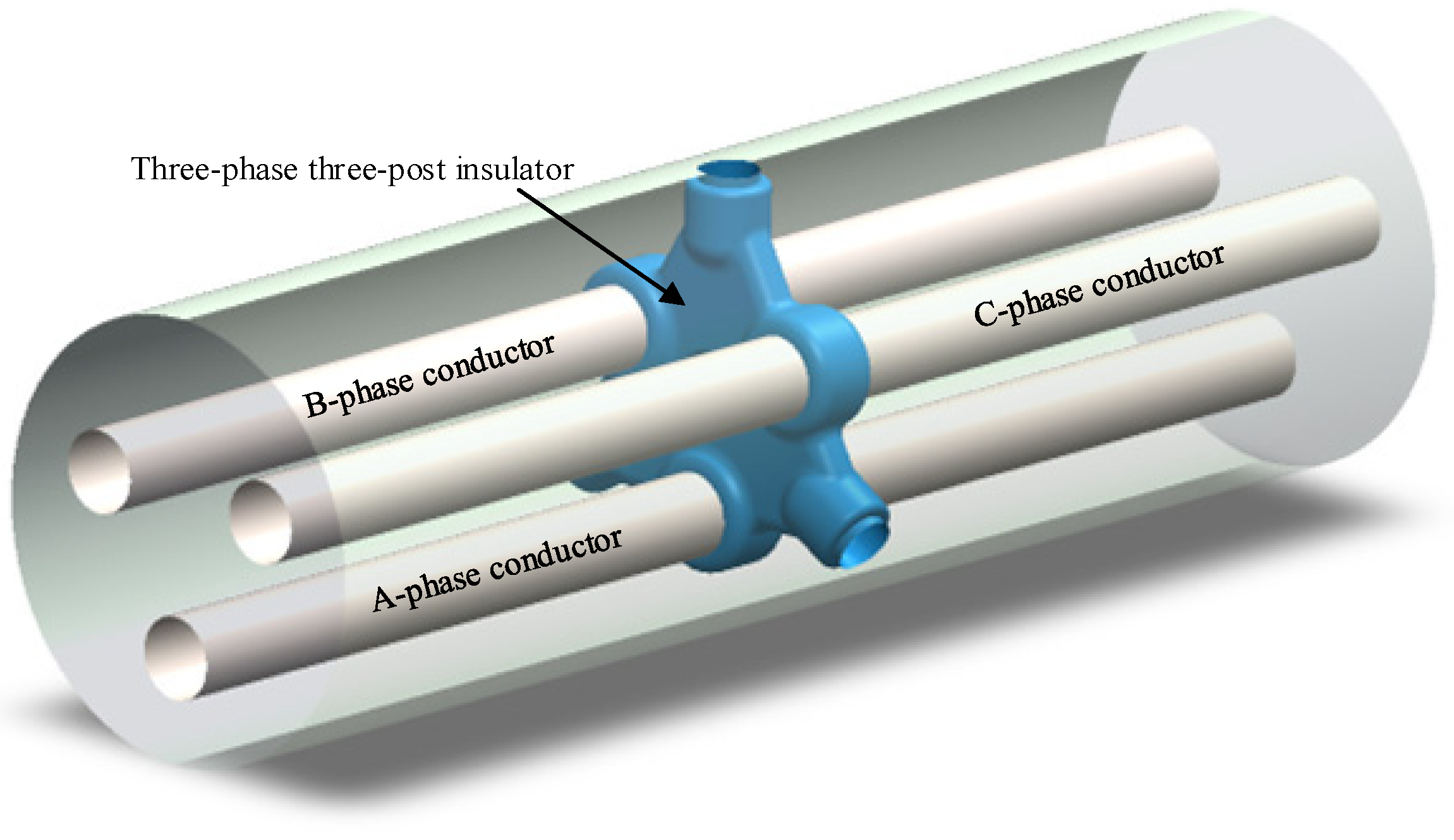
2. Model Construction and Parameter

2.1. Mathematical Modeling of Steady State Electric Field of Three-Phase Three-Post Insulators Under Industrial Frequency Voltage

This study investigates the electric field distribution of three-phase three-post insulators of gas-insulated transmission lines (GILs) in the presence of surface crack defects of different sizes and positions. Inside the insulators, the situation with air gap defects of different sizes and positions is also investigated.
The operating condition is 50 Hz industrial frequency voltage, and for the 252 kV voltage level of the GIL, Maxwell’s equations can be used to convert the electromagnetic field problem into a mathematical model that can be calculated. The electrostatic field is chosen as the computational model based on the fundamentals of the electrostatic field as well as the potential of the various defects under the various defects. Poisson’s equation is satisfied by the overall potential distribution of the insulator, while Laplace’s equation is satisfied for the region of the field where there is no free charge distribution.
2 φ = ρ ε
2 φ = 0
In Equations (1) and (2), ε represents the medium’s dielectric constant; φ is the potential; ∇² is the Laplace operator.
The electric field intensity and electric potential satisfy Equation (3). At the interface of multiple dielectric materials, the conditions (4) and (5) are satisfied.
E = φ
φ 1 = φ 2
ε 1 φ 1 n = ε 2 φ 2 n
E is the electric field strength, with units of kV/mm, and represents the relative dielectric constant of the insulating medium at the boundary between two materials. n is the normal vector of the interface.

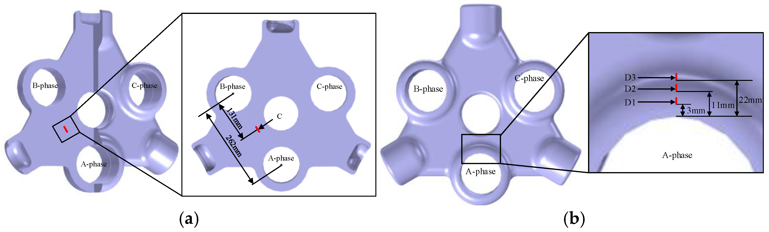
2.2. Simulation Modeling

In this work, a basic simulation model of a three-phase, three-post insulator with typical faults is built using a 252 kV GIL. It consists mainly of the conductor rod, the shell and the three-phase, three-post insulator, with 0.5 MPa SF6 filling the cavity. Figure 1 shows the overall simulation model. Figure 2 shows the dimensions of the three-phase, three-post insulator.
COMSOL Multiphysics is used for the simulation. The Electrostatics module is used to simulate the electric field. Considering the worst-case situation, the rated short-time power frequency withstand voltage rms value of 460 kV is selected for the 252 kV GIL. The peak value of the operating phase voltage Up is applied to one phase conductor, while −1/2 Up is applied to the other two-phase conductors. In particular, the enclosure is earthed, the potential of the A phase conductor is 650 kV, that of the B phase conductor is −326 kV and that of the C phase conductor is −326 kV.
Defects in gas-insulated, metal-encapsulated transmission lines can seriously distort the electric field distribution of the insulators and even lead to breakdown. The longer the defect on the surface of the central conductor, the higher the maximum value of the electric field [17]. Therefore, this article examines the progressive growth of air gap and crack defect sizes. The geometric shape of air gap defects is a capsule-shaped cylinder, and the geometric characteristics of air gap defects are shown in Figure 3. The shape of the air gap defect is shown in Figure 3a of this study, where length and diameter represent the length and diameter of the defect, respectively. Figure 3b shows the shape of the crack defect, where Height is the height of the defect, Width is the width of the defect and Depth is the depth of the defect.
Figure 4, Figure 5 and Figure 6 show the air gaps and crack defects at various locations in the three-phase, three-post insulator. Figure 4a is a schematic diagram of the insulator section T1. Figure 4b shows the distances L1 and L2, which are 13 mm and 26 mm, respectively, from the air gap flaws A4 and A1 to the insulator surface.
Free tetrahedral meshing is used to discretize the model mesh. Figure 7 shows how the mesh around the air gap defect is refined as a result of the distortion of the surrounding electric field.
In the simulation, the maximum and minimum mesh sizes for the air gap defect are 0.1 mm and 0.01 mm, respectively. For the SF6 gas domain, since the electric field transition is relatively smooth, a larger mesh size is used, with a maximum mesh size of 110 mm and a minimum of 8 mm. For the insulator, although the electric field transition is relatively smooth, the mesh should not be too large due to the presence of internal defects. In the simulation, the maximum and minimum mesh sizes for the insulator are 70 mm and 3 mm, respectively.

2.3. Material Parameters

The materials used in this study include aluminium alloy for the conductor rod and shell, epoxy resin for the insulator and air for the air gap defect. Table 1 lists the configurations of the material parameters.

3. Results and Analysis

3.1. Effect of Air Gap Defect Size and Location on Electric Field at Three-Phase Voltage

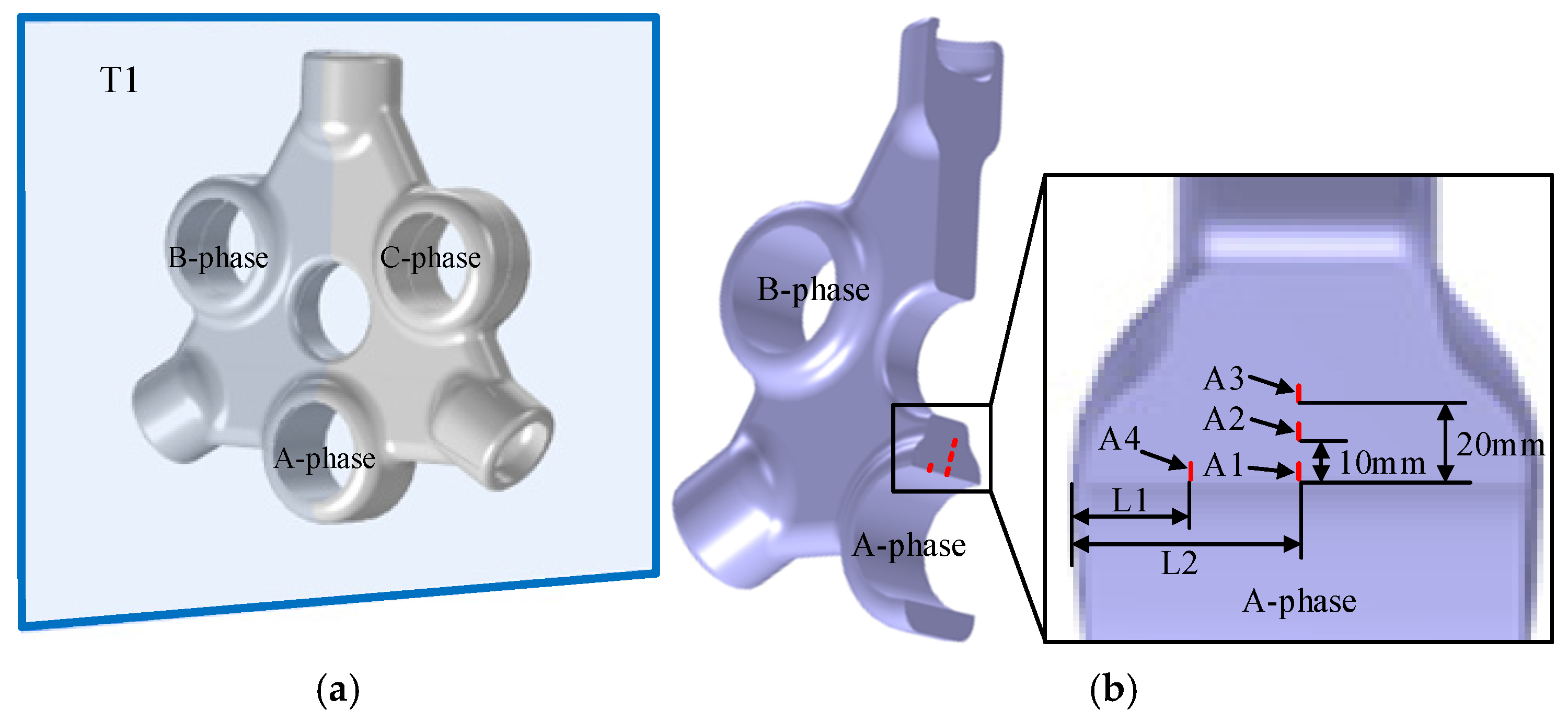
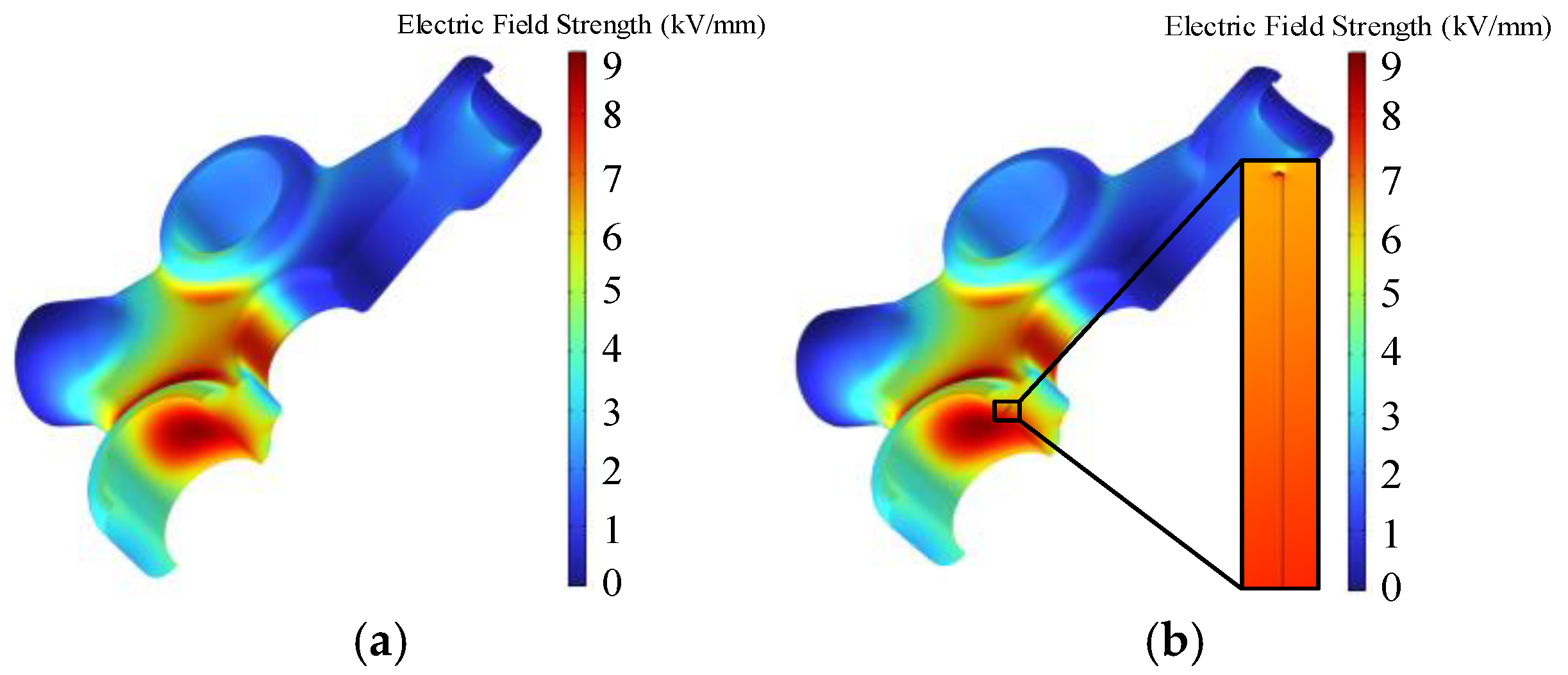
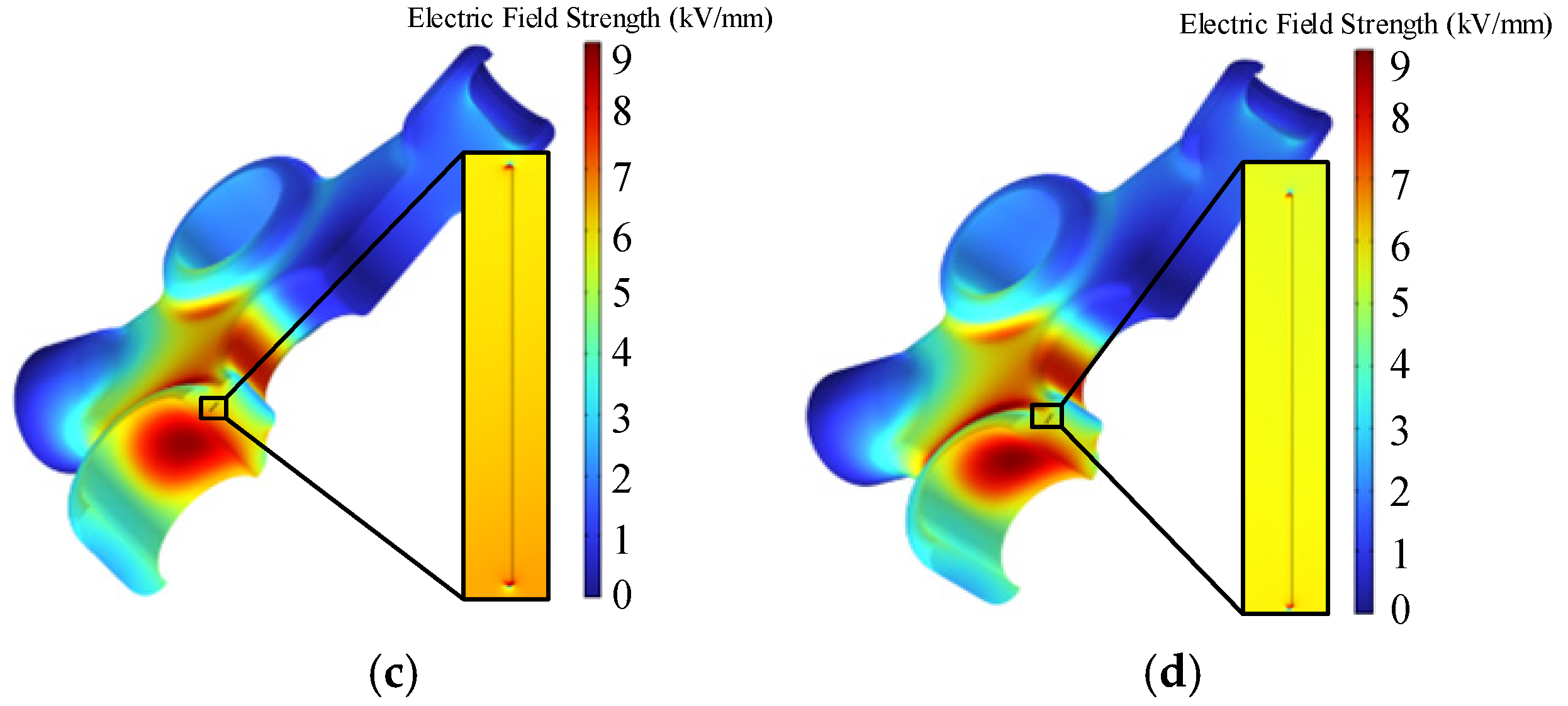
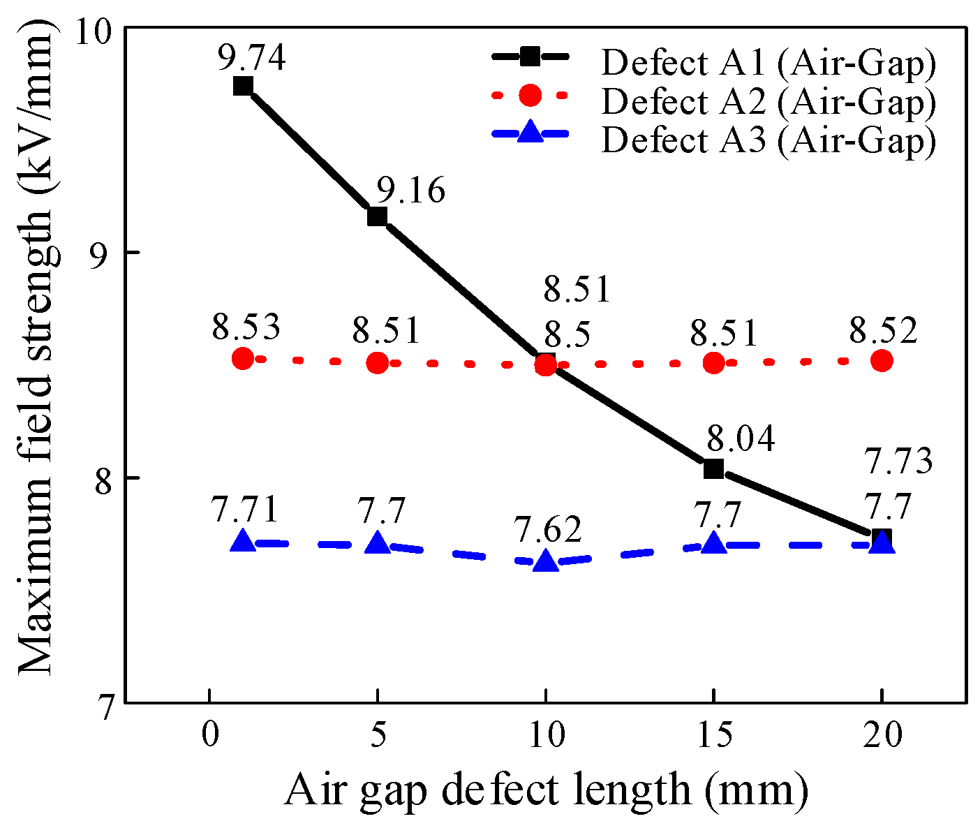
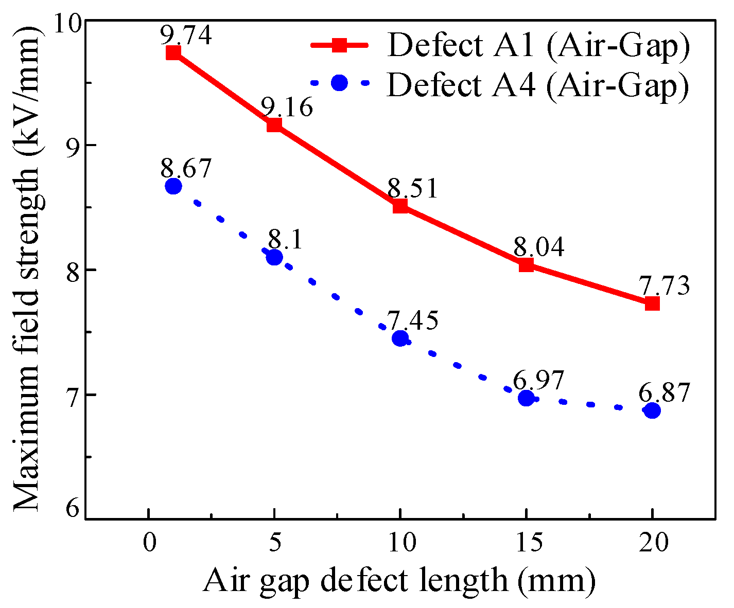
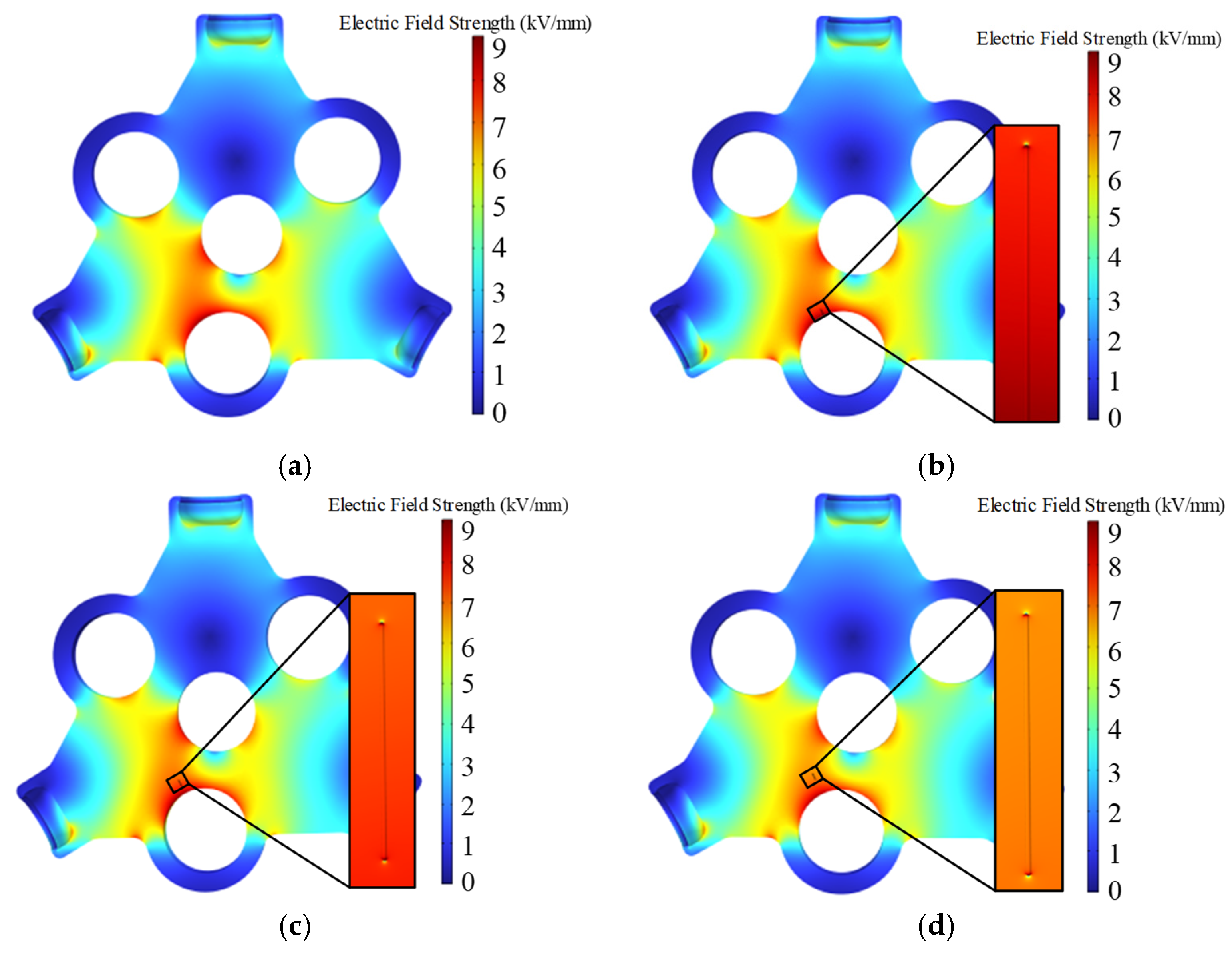
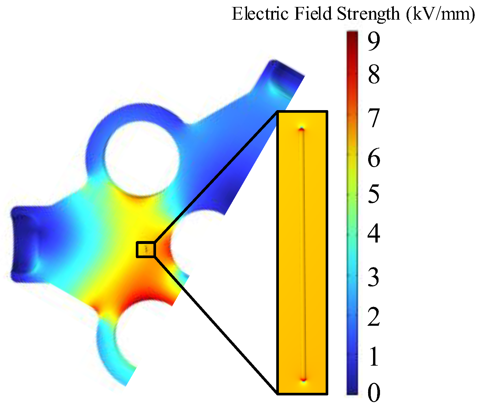
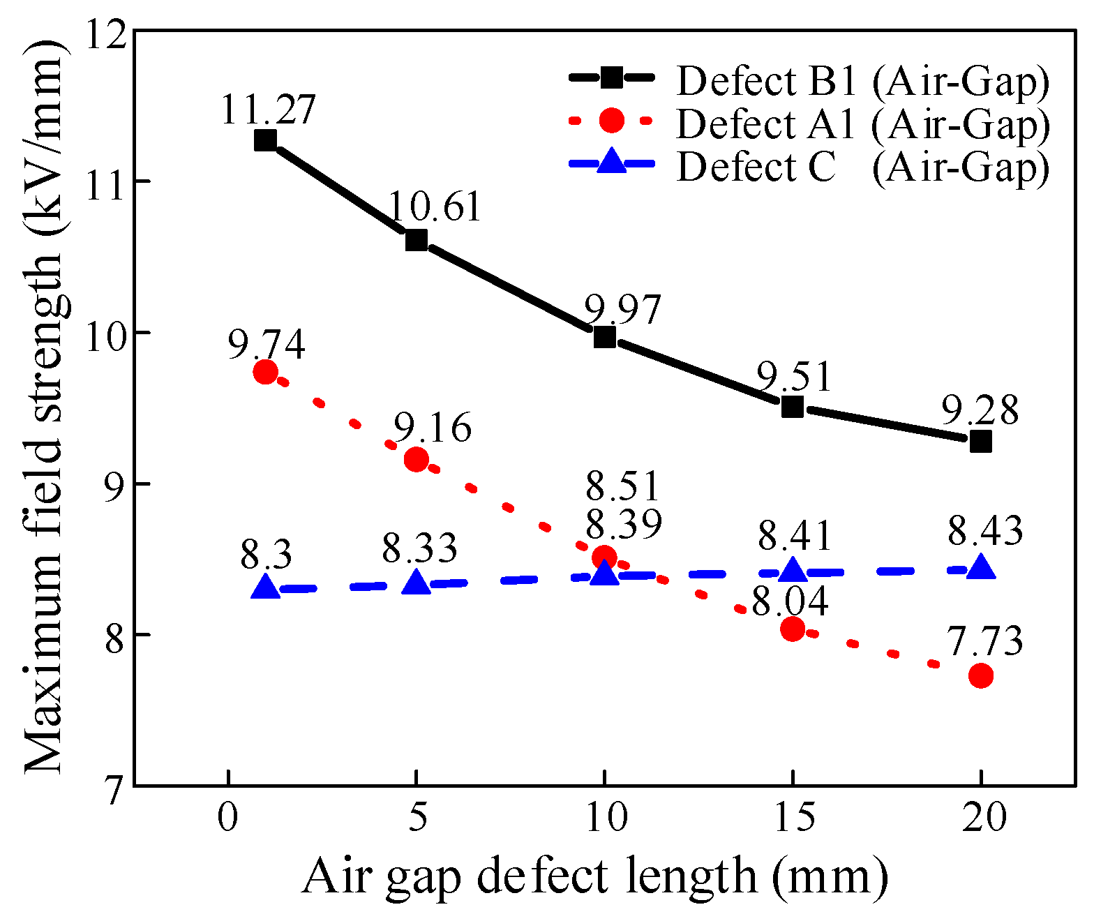
3.1.1. Air Gap Defects in Region A

The effects of the length and location of air gap defects on the electric field distribution in a given region are studied to resolve the non-uniformity of electric field distribution in three-phase three-post insulators. Inside the insulator near the conductor rod at position A are air gap defects A1, A2, A3 and A4, which have lengths of 1 mm, 5 mm, 10 mm, 15 mm and 20 mm, respectively. The variation curves of the maximum electric field intensity with the air gap parameters are then extracted, as shown in Figure 8, where the electric field intensity inside the air gap is significantly higher than that in the surrounding insulator. As shown in Figure 8, the electric field simulation is used to determine the electric field distribution under different air gap conditions. The concentration of the electric field in the air gap is caused by the fact that the dielectric constant of the air gap defects is significantly lower than that of the insulating material. When the air gap is at position A1, the maximum electric field strength decreases as the air gap length increases. The field strength of the 1 mm air gap is the highest at 9.74 kV/mm.
The maximum field strength is found in the 1 mm air gap defect at A1 with a maximum value of 9.74 kV/mm. Figure 9 shows that for the air gap defect at A1, the maximum field strength decreases as the air gap defect length increases. However, the maximum electric field strength remains essentially constant as the air gap defect length increases when the defects are located at A2 and A3. This is due to the following reasons: A1’s position is in an area with a large electric field gradient, so a change in air gap length will drastically alter the electric field distribution; A2 and A3’s positions have comparatively uniform electric field distributions, and the field strength of the defect is minimal. Figure 10 shows that the electric field is less affected by air gap defects that are closer to the insulator surface.
Since the air gaps in the A2 and A3 regions have less influence on the overall electric field strength, the manufacturing tolerance can be relaxed accordingly. Consequently, it is necessary to pay attention to the air gap defects in the high electric field gradient region during insulation design in order to prevent partial discharge or breakdown caused by tiny air gaps.

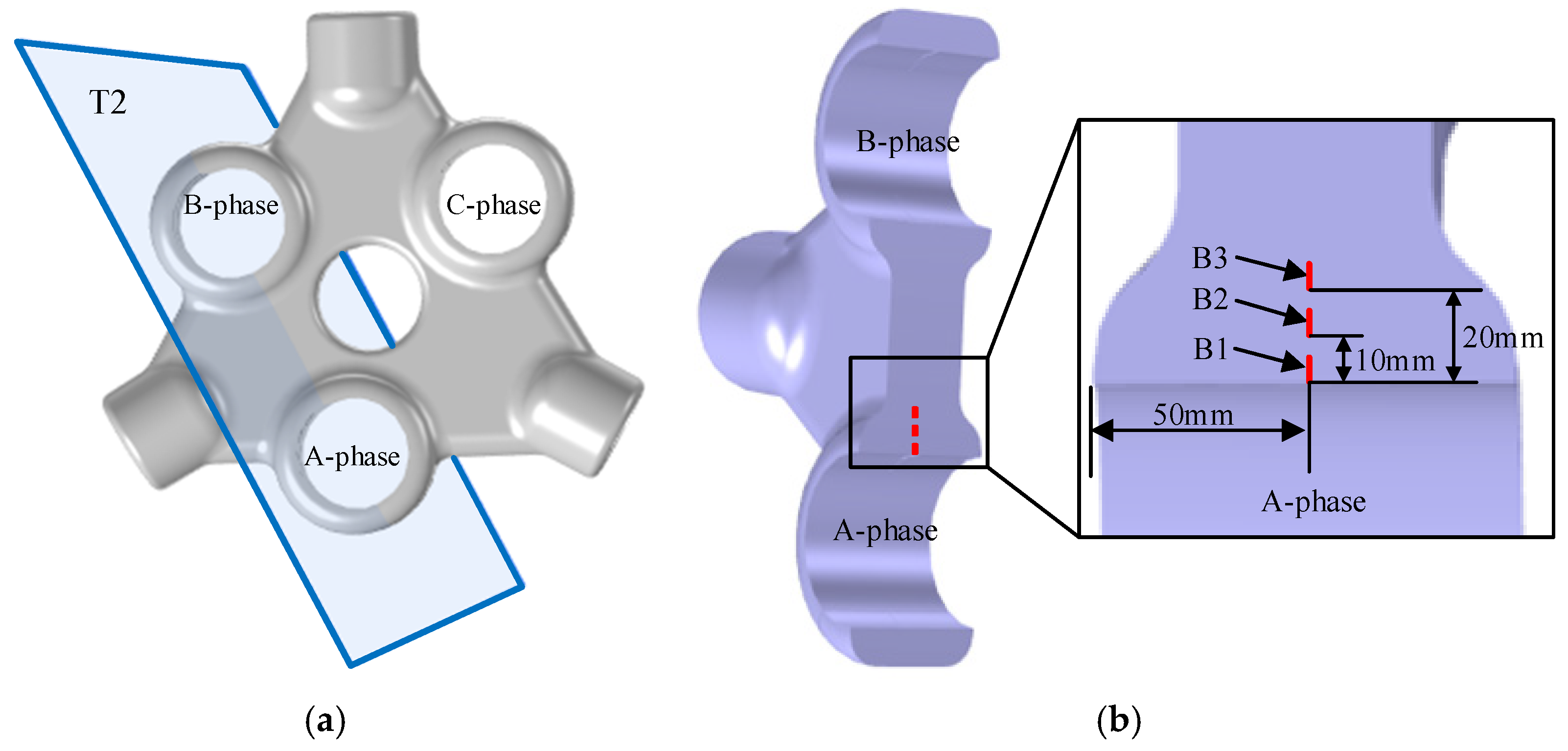
3.1.2. Air Gap Defects in Region B

Inside the insulator, near the conductor at position B, there are air gap defects B1, B2 and B3 with lengths of 1 mm, 5 mm, 10 mm, 15 mm and 20 mm, respectively. Electric field simulation is used to determine the electric field distribution under different air gap conditions, as shown in Figure 11. The variation curves of the maximum electric field intensity with the air gap parameters are then extracted, as shown in Figure 12, which shows that the electric field intensity inside the air gap is significantly higher than that in the surrounding insulator. To investigate the cause, the electric field concentration in the air gap is caused by the dielectric constant of the air gap defects being significantly smaller than that of the insulating material.
According to Figure 12, the maximum field strength in the 1 mm air gap defect is found at B1, with a maximum value of 11.27 kV/mm. When the air gap defect is located at B1, the maximum field strength decreases as the length of the air gap defect increases. However, the maximum electric field strength remains essentially the same as the length of the air gap defect increases when it is at B2 and B3. According to an analysis of the causes, the B1 position is in an area with a high electric field gradient, and the distribution of the electric field changes significantly when the air gap length changes. In contrast, positions B2 and B3 have a more uniform electric field distribution and the field strength is less affected by the air gap length.
In conclusion, the surrounding electric field is most affected when the air gap defect occurs in the B region. Therefore, the voltage of the B conductor is changed to investigate the effect of the voltage polarity on the electric field of the air gap defect in more detail. In other words, the voltage of phase A changes from 650 kV to −326 kV, the voltage of the B conductor changes from −326 kV to 650 kV, and the voltage of phase C remains at −326 kV. As shown in Figure 13, the influence of the B conductor on the electric field increases when its voltage reaches 650 kV.

3.1.3. Air Gap Defects in Region C

The results of the electric field simulation are shown in Figure 14 when the air gap defect is located in the centre of the high and low voltage bars. It can be seen that the electric field inside the air gap is much larger than that inside the insulator surrounding the air gap. In contrast, the air gap defects in regions A, B and C, as shown in Figure 15, have the most significant effect on the electric field when they are closer to the bus bars. Of these, the air gap defects in B1 have the greatest effect on the electric field.

3.1.4. Impact of Air Gap Defect Radius on Electric Field Distribution

Air gap defects with a length of 10 mm and a progressively increasing radius are placed at position A inside the insulator near the conductor rod to study the effect of the defect radius on the electric field. The radius increases over time from 0.1 mm to 2 mm. The diameter increases over time from 0.2 mm to 4 mm. Figure 16 shows the relationship between the radius of the air gap defect and the electric field strength. It can be seen that air gap defects between 0.1 and 2 mm have a relatively similar effect on the electric field.

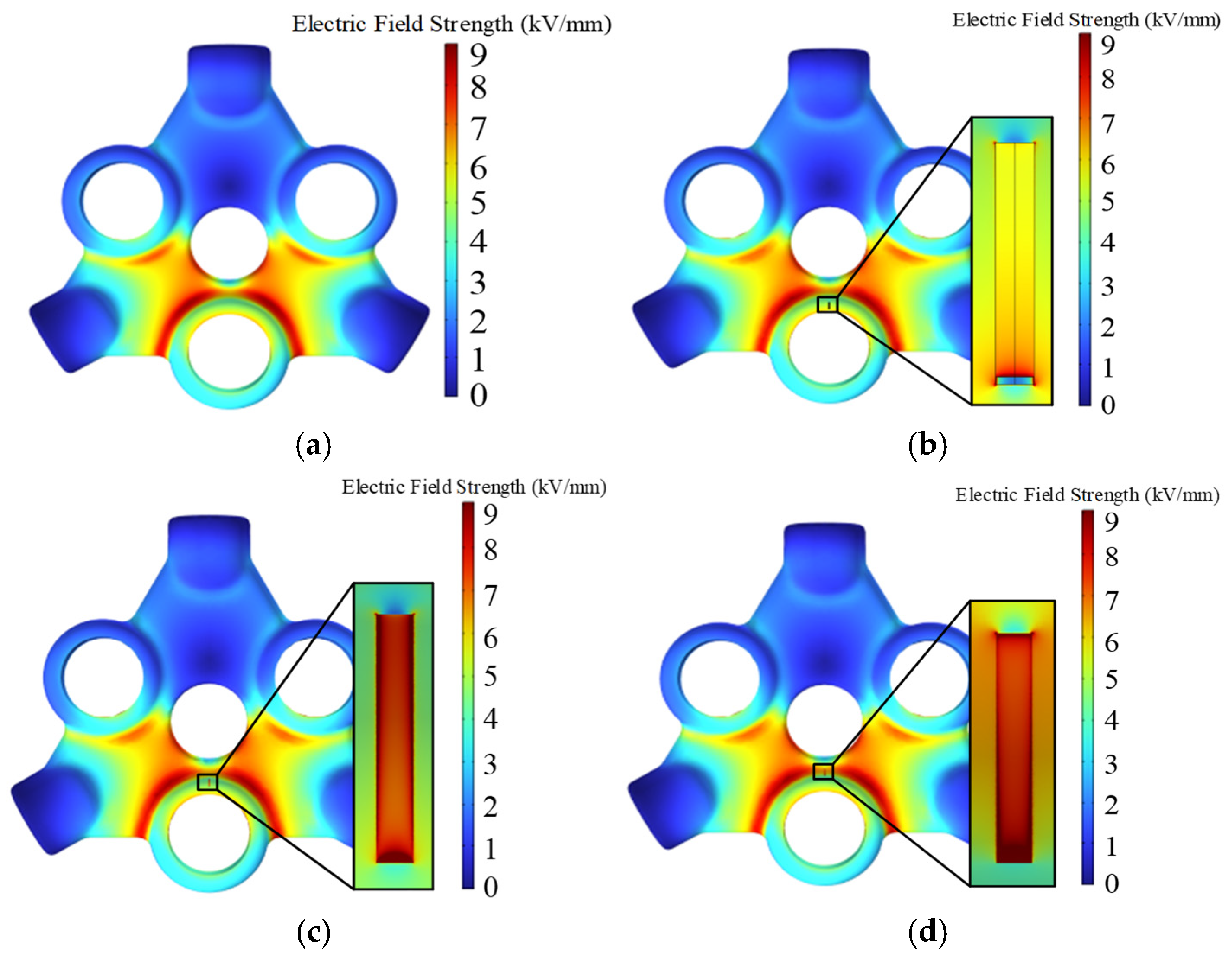
3.2. Effect of Crack Defect Size and Location on Electric Field at Three-Phase Voltage

3.2.1. Effect of Crack Defect Location on Electric Field

Crack defects D1, D2 and D3 with heights of 10 mm, depths of 10 mm and widths of 1.5 mm are placed on the insulator surface D to investigate the effect of the crack defect location on the electric field distribution. Figure 17 shows the results of the electric field simulation, while Figure 18 shows the variation in the maximum electric field intensity with the crack position.
The electric field at the cracks and the distortion of the surrounding electric field are caused by the defects of the insulator surface cracks. The crack defect at D2 has the greatest effect on the surrounding electric field.

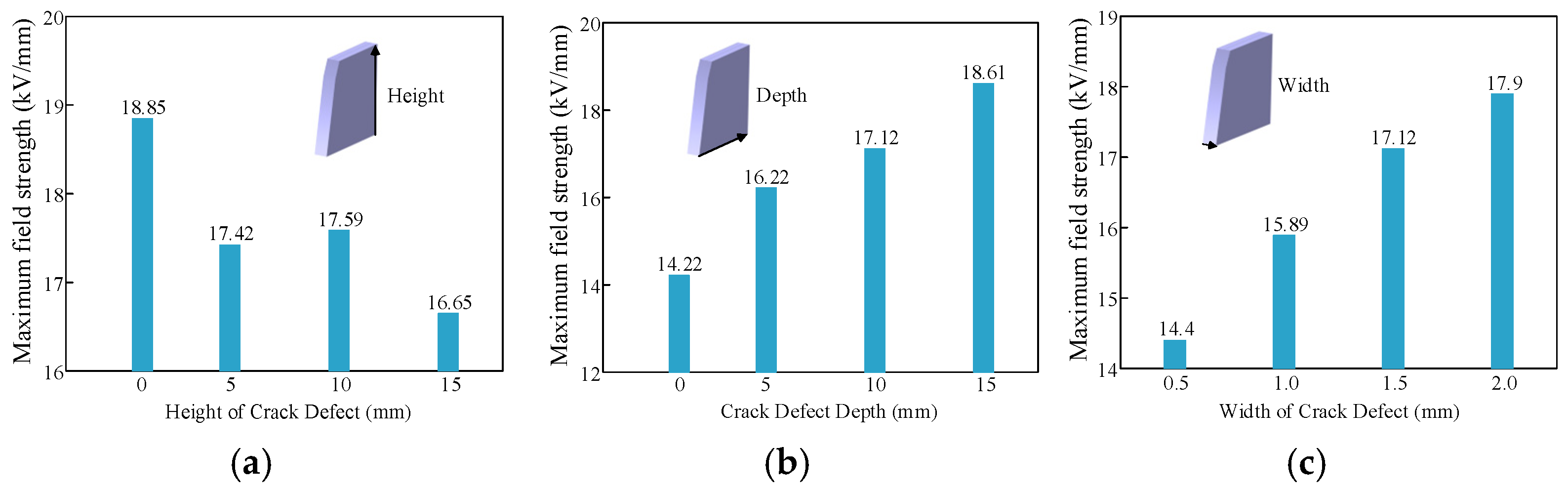
3.2.2. Effect of Crack Defect Size on Electric Field

A controlled variable approach was used to investigate how the size of the crack defects affected the surrounding electric field. The width, depth and height of the D1 crack defect were varied to determine how these characteristics affected the surrounding electric field; the results of the electric field simulation are shown in Figure 19.
The perturbation of the surrounding electric field is greater the deeper the crack (up to a maximum of 10 mm), which causes the field intensity to increase significantly. The spectrum of electric field perturbation is broadened and the peak field intensity increases with increasing width (up to 1.5 mm). In fact, there is a negative correlation between height (from 1 mm) and the effect on the electric field. Regarding the combination of peak field strength, as shown in Figure 19, the field strength increases to 18.85 kV/mm when the height, width and depth are 1 mm, 1.5 mm and 10 mm, respectively.
  • Effect of depth: The electric field gradient near the conductor, as the depth of the crack increases, moves closer to the high potential conductor, which increases the local electric field gradient. Field accumulation effect: Charge accumulates at the bottom of deep cracks, extending the path of electric field distortion and increasing the concentration of field strength.
  • Width effect: Lateral growth of electric field coverage. The area of high field strength is substantially increased as the width increases because more electric field lines can flow through the insulating material on either side of the crack. Polarisation of the dielectric interface: The electric field distortion is exacerbated by the larger air–insulator interface created by a wider crack.
  • Effect of height: Change in geometric aspect ratio: As the height increases, the aspect ratio of the crack (height/width) decreases, reducing the tip curvature effect and easing the field strength concentration. Dispersion of the longitudinal electric field distribution: The internal electric field lines of a tall crack are more widely distributed, reducing local peaks.

4. Conclusions

In this study, a computational model for simulating the electric field of a 252 kV three-phase three-post insulator is established using finite element analysis and three-dimensional mapping software. The effects of the geographical locations and dimensional characteristics (length, width, depth and radius) of the air gap and crack defects on the electric field distribution are methodically investigated. The conclusions are as follows:
  • The location of air gap defects affects the electric field. The electric field distortion is most pronounced in the vicinity of the high-voltage conductor rod (B1, A1). For example, an A1 mm air gap at B1 has an electric field strength of 11.27 kV/mm. The air gap defects have less effect on the electric field strength in the low voltage or uniform field area (A2, A3, B2, B3).
  • The electric field is affected by the size of the air gap defects. (1) Length: The peak electric field strength decreases (from 11.27 to 8.28 kV/mm) in the high gradient area (such as B1) as the air gap length increases (from 1 to 20 mm). The electric field strength remains essentially constant with length in a homogeneous field region (e.g., A2, A3, B2, B3). (2) Radius: When the radius is between 0.1 and 2 mm, there is minimal variation in the electric field strength. (3) Voltage polarity: On the high-voltage side (e.g., 11.27 kV/mm), the electric field distortion of the same air gap defect is much larger than on the low-voltage side (e.g., 8.65 kV/mm).
  • The location of crack defects affects the electric field. Surface crack defects in the D1 and D3 regions have less effect on the surrounding area than the D2 region on the strength of the surrounding electric field.
  • The electric field is affected by the size of the crack defects. (1) Height: The maximum value of the electric field strength decreases from 18.85 kV/mm to 16.65 kV/mm as the height increases. (2) Width: The range of electric field distortion widens and the peak value increases to 17.9 kV/mm as the width increases (from 0.5 to 2.0 mm). (3) Depth: As the depth increases (from 1 to 15 mm), the electric field strength also increases, reaching a peak value of 18.61 kV/mm and bringing the bottom of the crack closer to the conductor rod.

Author Contributions

Z.Y., Conceptualization, investigation, writing—original draft and funding acquisition; L.L. and H.W., software, validation, data curation and visualization; Y.W. and J.L., Methodology, formal analysis; H.L., writing—review and editing; X.L., Resources, project administration and supervision. All authors have read and agreed to the published version of the manuscript.

Funding

This research was funded by the Key Science and Technology Project of State Grid Jiangsu Electric Power Co., Ltd. (J2024121).

Data Availability Statement

The original contributions presented in this study are included in the article. Further inquiries can be directed to the corresponding author.

Conflicts of Interest

Zhuoran Yang, Lixiang Lv, Hao Wang, Yue Wang, Jian Liu and Hongze Li were employed by the State Grid Nanjing Power Supply Company. The remaining authors declare that the research was conducted in the absence of any commercial or financial relationships that could be construed as a potential conflict of interest.

References

  1. Xiao, D.M.; Yan, J.D. Application and development of gas-insulated transmission lines (GIL). High Volt. Eng. 2017, 43, 699–707. [Google Scholar]
  2. Zhang, C.H.; Zhang, B.Y.; Li, M.Y.; Li, Y.X.; Li, X.W.; Lv, J.Z.; Wang, Z.G.; Li, W.G.; Yang, X. Review of Key Insulation Technologies of HVDC GIL. High Volt. Eng. 2023, 49, 920–936. [Google Scholar]
  3. Peng, Z.R.; Zhang, P.F.; Liu, P.; Hang, X.C.; Yang, B.L.; Cui, B.Y.; Wu, Z.H.; Tian, H.D.; Wang, H.R. Key Insulation Technology of UHV GIL in Sutong Utility Tunnel Project. High Volt. Eng. 2023, 49, 4046–4057. [Google Scholar]
  4. Zhou, Y.X.; Chen, J.N.; Zhang, L.; Zhang, Y.X.; Teng, C.Y.; Huang, X. Opportunity for Developing Ultra High Voltage Transmission Technology Under the Emission Peak, Carbon Neutrality and New Infrastructure. High Volt. Eng. 2021, 47, 2396–2408. [Google Scholar]
  5. Xing, Y.; Wang, Z.; Liu, L.; Xu, Y.; Yang, Y.; Liu, S.; Zhou, F.; He, S.; Li, C. Defects and failure types of solid insulation in gas insulated switchgear: In situ study and case analysis. High Volt. 2022, 7, 158–164. [Google Scholar] [CrossRef]
  6. Li, X.; Yin, Y.C.; Wang, Y.; Bian, Y.L.; Li, Q.M.; Wang, J. Adsorption Behavior and Flashover Characteristics of DC GIL Metal Particles/Dust Facing Tri-post Insulator. High Volt. Eng. 2025, 3, 1–12. [Google Scholar]
  7. Li, X.; Ding, D.W.; Wu, C.Q.; Xu, Y.; Tang, G. Research on the Partial Discharge Development and Flashover Characteristics of Metal Particle on a 550 kV GIL Triple Post Insulator Surface. Proc. CSEE 2025, 3, 1–10. [Google Scholar]
  8. Shu, T.; Yang, Y.P.; Guo, R.T.; Wu, J.C.; Zhang, X.R.; Li, J.H. Partial Discharge Excitation Characteristics of Free Metal Particles in SF6 Gas Under AC and Negative Lightning Impulse Superposition Voltage. High Volt. Eng. 2022, 48, 3305–3315. [Google Scholar]
  9. Xu, J.Y.; Wang, F. Three Dimensional ElectricField Calculation of the Disk Type Insulator inside of Three Phase in one Tank Type of GIS. High Volt. Eng. 2000, 1, 11–13. [Google Scholar]
  10. Wu, Z.H.; Tian, H.D.; Jin, S.F.; Zhu, S.J.; Wang, H.R.; Peng, Z.R. Design and Optimization of Insulation Structure of Three-phase Tri-post Insulator in 252 kV Compact GIL. High Volt. Eng. 2020, 46, 2030–2039. [Google Scholar]
  11. Li, J.H.; Han, X.T.; Liu, Z.H.; Li, Y.M. A review of partial discharge detection techniques for electrical equipment. High Volt. Technol. 2015, 41, 2583–2601. [Google Scholar]
  12. Li, C.L.; Liu, R.; Li, P.H.; Li, W.P.; Gao, N.K. Electric Field Simulation of Typical Defects in the Epoxy/Paper Composites Insulated Tubular Bus. Mater. Sci. Forum 2018, 4538, 157–162. [Google Scholar] [CrossRef]
  13. Wang, H.M.; Ding, D.W.; Jia, Z.J.; Tang, M.Z.; Zhao, C.H.; Tang, Z.G. Study on the long intermittent discharge characteristics of GIS basin-type insulator surface defects under constant pressure. Proc. CSEE 2018, 38, 6188–6194. [Google Scholar]
  14. Luo, S.; Luan, L.; Cui, Y.; Xu, S.; Guo, Q.; Liu, T. Influence of typical composite insulators defects on axial temperature based on simulation analysis. IOP Conf. Ser. Earth Environ. Sci. 2021, 769, 042044. [Google Scholar] [CrossRef]
  15. He, B.N.; Kong, J.; Ning, J.X.; Wang, Z.Z.; Wang, L.M.; Xie, Y.D.; Hung, D.C. Electric field simulation analysis of basin-type insulators with bubble defects. Insul. Mater. 2019, 52, 86–92. [Google Scholar]
  16. He, B.N.; Kong, J.; Jiang, R.Z.; Ning, J.X.; Wang, L.M.; Xie, Y.D.; Huang, G.C. Electric field distribution simulation study under metal wire defects of basin-type insulators. Insul. Mater. 2021, 54, 39–44. [Google Scholar]
  17. Ueta, G.; Wada, J.; Okabe, S.; Miyashita, M.; Nishida, C.; Kamei, M. Insulation characteristics of epoxy insulator with internal void-shaped micro-defects. IEEE Trans. Dielectr. Electr. Insul. 2013, 20, 535–543. [Google Scholar] [CrossRef]
  18. Qi, B.; Li, C.R.; Hao, Z.; Geng, B.B.; Xu, D.G.; Liu, S.Y.; Deng, C. Phenomenon and characteristics of surface partial discharge development along fixed metal particles on GIS insulators. Proc. CSEE 2011, 31, 101–108. [Google Scholar]
  19. Zhou, Q.; Tang, J.; Tang, M.; Xie, Y.B.; Liu, M.J. Mathematical model of partial discharge ultra-high frequency for four typical defects in GIS. Proc. CSEE 2006, 08, 99–105. [Google Scholar]
  20. Tian, F.; Hao, Y.; Zou, Z.; Zheng, Y.; He, W.; Yang, L.; Li, L. An Ultrasonic Pulse-Echo Method to Detect Internal Defects in Epoxy Composite Insulation. Energies 2019, 12, 4804. [Google Scholar] [CrossRef]
  21. Ding, D.W.; Gao, W.S.; Liu, W.D. Analysis of typical defects in GIS using ultra-high frequency method. High Volt. Technol. 2011, 37, 706–710. [Google Scholar]
  22. Zou, Z.; Hao, Y.; Tian, F.; Zheng, F.; He, W.; Yang, L.; Li, L. An Ultrasonic Longitudinal Through-Transmission Method to Measure the Compressive Internal Stress in Epoxy Composite Specimens of Gas-Insulated Metal-Enclosed Switchgear. Energies 2020, 13, 1248. [Google Scholar] [CrossRef]
  23. Xu, W.H.; Li, W.B.; Jiang, W.J.; Li, X.L.; Wang, W.S. Research on Typical Decay-like Fracture Defects of Composite Insulators Based on Electro-Thermal Coupling. Electronics 2024, 13, 4495. [Google Scholar] [CrossRef]
Figure 1. Global model.
Energies 18 02344 g001
Figure 2. The dimensions of the three-phase three-post insulator.
Energies 18 02344 g002
Figure 3. (a) The shape of air gap defects. (b) The shape of crack defects.
Energies 18 02344 g003
Figure 4. (a) Schematic diagram of the insulator cross-section T1. (b) Air gap defects in region A.
Energies 18 02344 g004
Figure 5. (a) Schematic diagram of the insulator cross-section T2. (b) Air gap defects in region B.
Energies 18 02344 g005
Figure 6. (a) Air gap defects in region C. (b) Crack defects in region D.
Energies 18 02344 g006
Figure 7. (a) Overall model mesh discretization. (b) Mesh discretization of insulators and air gap defects.
Energies 18 02344 g007
Figure 8. (a) Defect-free electric field distribution. (b) Electric field distribution at air gap defect at position A1. (c) Electric field distribution at air gap defect at position A2. (d) Electric field distribution at air gap defect at position A3.
Energies 18 02344 g008aEnergies 18 02344 g008b
Figure 9. Variation curves of electric field strength with air gap defect length and location in area A.
Energies 18 02344 g009
Figure 10. Variation curve of the maximum electric field strength of the air gap defect with its distance to the insulator surface.
Energies 18 02344 g010
Figure 11. (a) Defect-free electric field distribution. (b) Electric field distribution at air gap defect at position B1. (c) Electric field distribution at air gap defect at position B2. (d) Electric field distribution at air gap defect at position B3.
Energies 18 02344 g011
Figure 12. Variation curves of electric field strength with air gap defect length and location in area B.
Energies 18 02344 g012
Figure 13. Variation curves of the maximum electric field strength of air gap defects with length under different voltages of the B conductor.
Energies 18 02344 g013
Figure 14. Electric field distribution at air gap defect at position C.
Energies 18 02344 g014
Figure 15. Variation curves of electric field strength with air gap defect length and location.
Energies 18 02344 g015
Figure 16. Variation curves of electric field strength with air gap defect radius.
Energies 18 02344 g016
Figure 17. (a) Defect-free electric field distribution. (b) Electric field distribution at air gap defect at position D1. (c) Electric field distribution at air gap defect at position D2. (d) Electric field distribution at air gap defect at position D3.
Energies 18 02344 g017
Figure 18. Variation curve of the maximal electric field intensity and the location of the cracks.
Energies 18 02344 g018
Figure 19. (a) Curve of electric field strength as a function of crack defect height. (b) Curve of electric field strength as a function of crack defect depth. (c) Curve of electric field strength as a function of crack defect width.
Energies 18 02344 g019
Table 1. Material parameters.
MaterialRelative Permittivity
Aluminum Alloy1
Epoxy Resin4.975
SF61
Disclaimer/Publisher’s Note: The statements, opinions and data contained in all publications are solely those of the individual author(s) and contributor(s) and not of MDPI and/or the editor(s). MDPI and/or the editor(s) disclaim responsibility for any injury to people or property resulting from any ideas, methods, instructions or products referred to in the content.

