1. Introduction
The current geopolitical situation and the latest guidelines and requirements of the European Union and NATO are key determinants of the creation of new material and technological solutions for military and non-military security. Energy, ecological, and cyber security are key challenges facing the world to ensure peace [
1,
2,
3].
It is not without reason that the reality of the 21st century world is called VUCA: Volatility, Uncertainty, Complexity, and Ambiguity. In this context, advanced electronic and photonic technologies play a key role, enabling society to understand better, adapt and respond to an environment that is changing at a speed unprecedented in previous decades. Considering the above, issues related to devices for generating and storing electricity and detecting faults become essential. Our interests focus on the modification of photovoltaic panels and sensors for civilian and military applications through the use of nanomaterials and polymers.
Failure-free operation of photovoltaic panels is a condition for effective operation energy generation, long service life, and quick return on investment. A simple and reliable evaluation method is required to ensure trouble-free operation of solar panel performance both in the production process and after installation. Currently, thermal imaging cameras are widely used in panel examinations of solar panels in the production process and for control tests and maintenance after panel installation. Because there are flaws in the panel that are clearly visible in the thermal image, thermal cameras can be used to scan large surfaces of installed solar panels over time for normal operation. Thermal imaging cameras are portable and lightweight, and they allow for their use in the field. However, they always require a scan of the panels—their surface—by the user at their location. This non-contact and non-invasive inspection method provides valuable insights into the thermal behaviour of solar panels, helping to identify issues that have an impact on their efficiency and longevity. The basis of this technique concentrates on the capture and visualization of heat emitted by objects using an infrared camera as a detector. This technology allows for the detection of temperature anomalies, compared to that of properly working objects, that are not visible to the naked eye. The major advantages of thermal imaging in photovoltaic systems are the possibility of non-destructive testing, real-time analysis, cost-effectiveness, and versatile deployment [
4,
5,
6,
7].
On the other hand, sensors are devices that detect and measure the physical properties of the environment, converting this information into electrical or optical signals that can be interpreted by computer systems or other devices [
8]. Sensors play a key role in monitoring and automating various processes, from industry to medicine. Some examples of sensor applications are presented in
Table 1 based on literature analysis [
9,
10,
11,
12,
13,
14,
15,
16,
17,
18,
19,
20,
21,
22,
23,
24,
25,
26,
27,
28,
29].
Methods for detecting mechanical damage to photovoltaic (PV) panels can be divided into several groups based on methodology and testing technique: visual inspection of the panels, acoustic testing, testing of panel output voltage and current, resonance testing, thermography, or microscopic techniques. Monitoring of cracks, scratches, chips, dents, or other visible damage to the surface of the panels can also be performed using drones with image analysis software [
30]. Moreover, one promising approach that attracted significant attention is the use of new exposure-monitoring tools—sensors for monitoring airborne pollutants, environmental conditions, physical agents, and workers’ postures. Next-generation monitors and sensors are essential for future occupational risk assessments [
31]. Additionally, there are patented solutions for devices for monitoring PV panels [
32,
33,
34,
35].
For example, in [
32], a device for monitoring photovoltaic panel modules in the event of theft or damage was constructed and investigated by monitoring the DC voltage in case of damage or theft. The signal is encoded for each panel sent to the central alarm device located next to the inverter and has a decoder that triggers an alarm for the panel in case the voltage residual generated by solar panels drops to zero. Another solution was proposed in [
33], where photovoltaic module error detection processing was investigated. The PV module comprised a plurality of cell panels connected in series, where each cell panel includes an input end and an output end, a self-control module, and an emergency module. It was placed on each short-circuit wire on and off unit, and controllers controlled disconnection and connection units.
Moreover, a self-controlled photovoltaic module was also investigated in [
34]. The module includes a junction box and side plates, wherein the junction box is placed, a battery string assembly, a self-damage monitoring device, and a single photovoltaic module. The measurement circuit consists of a circuit board current, a voltage detection, acquisition, and a manual switch connected in series.
Additionally, a system for monitoring the operation and optimization of a set of photovoltaic panels enabling detection and prediction of damage was studied in [
35]. The module communication monitoring takes placed via radio, including precisely set time intervals in which individual addresses and logical locations correspond to the physical location of the monitoring modules relative to each other. In the system, PV module parameters are controlled by using a voltage–current measurement circuit, which stores these parameters in the microcontroller’s memory. Data are transmitted via radio using a wireless communication module with an antenna communication in a synchronized manner based on information from the coordinator networks.
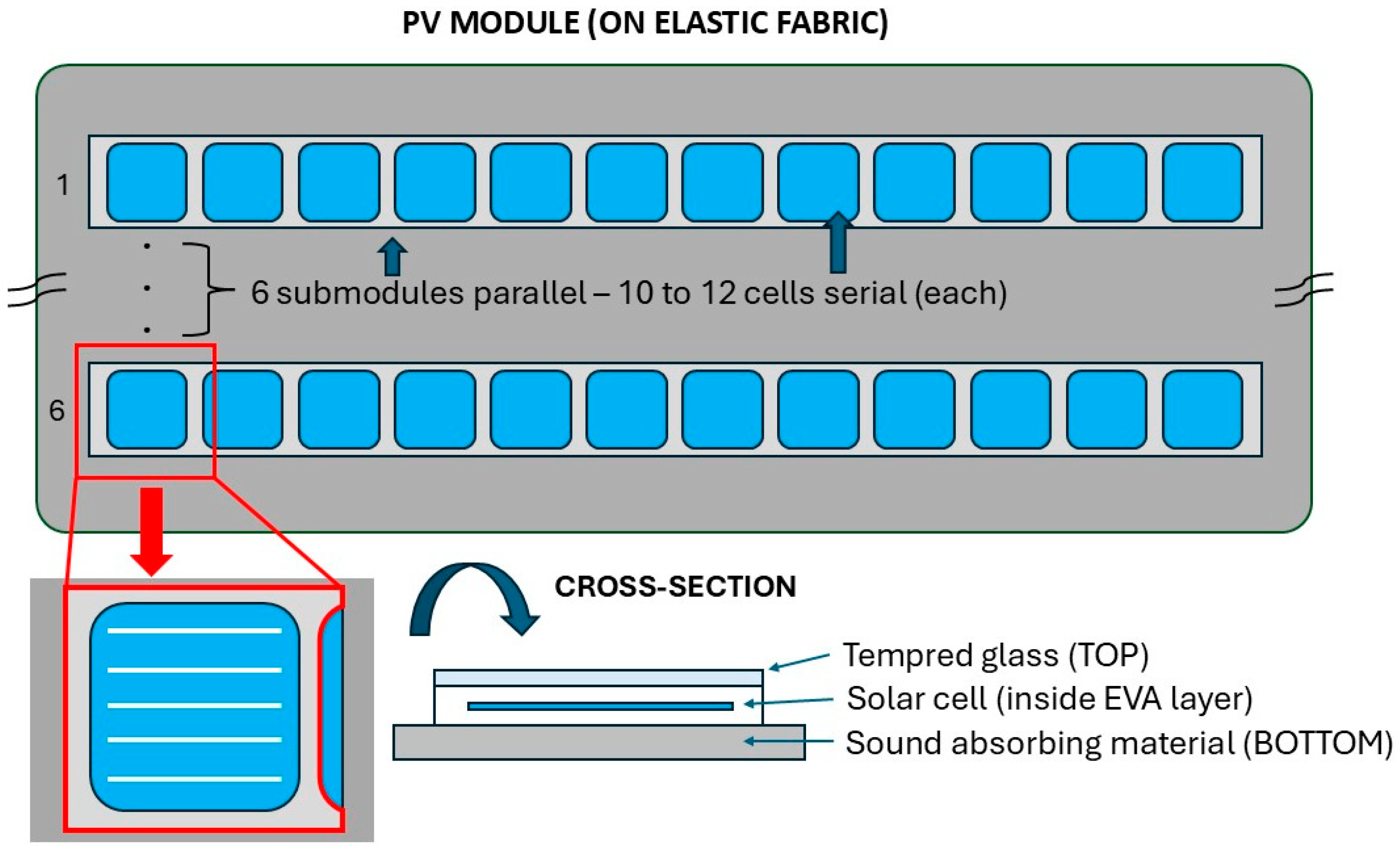
Finally, we stress that a lot of work is also dedicated to improve the properties of PV panels for practical use. The most commonly produced and currently assembled type of photovoltaic module is one that consists of a front glass, solar cells, the backside protective layer, and the characteristic element—the aluminum support frame. Such a PV module can be mounted on dedicated constructions or buildings (Building-Applied Photovoltaics). Another interesting type of building structures are sound-absorbing screens mounted along roads or tracks. Acoustic screens are constructed of elements with specific sound absorption properties. The efficiency of these screens depends primarily on their geometry and the sound source—the receiver layout, provided that they meet the minimum values for their sound insulation and the ability to absorb sound. In the case of railway acoustic screens, one-sided absorbing screens are most often used, with the absorbing side placed on the side of the track. For this reason, mounting on their typical PV modules is impossible because they block the absorption of the sound. The solution can be a new PV module set on a flexible substrate. The PV module can be designed to cover acoustic screens standing along railway lines. An important novelty is the use of elastic fabric as a buoyant substrate and the division of the PV module into submodules, which is within the scope of our interests (
Figure 1).
The module is supposed to produce electricity and be part of the acoustic screen and thus cannot significantly change its acoustic parameters. The PV module’s innovative design and its sound-reflecting and sound-absorbing parameters became the basis for obtaining two patents [
36,
37]. This was published in our last paper [
38]. Changes in the design of the PV module mean that the biggest challenge is to produce it in such a way that its durability is comparable to typical PV modules. Another challenge is monitoring the status of modules when operating in unusual conditions. Such conditions occur on the acoustic screens when very fast trains pass. Therefore, monitoring module damage is even more important than in the case of typical PV installations.
This type of sensor can be applied in PV modules used by the Armed Forces. Such systems must operate in highly unusual conditions, including on the battlefield. In such cases, the modules are exposed to damage or destruction. Rapid diagnostics of potential damage allows for a quick response, enabling effective command and communication. The successful execution of combat missions requires communication that ensures information transfer between superiors and subordinates, which is only possible when there is access to power for military equipment. Additionally, they can be used in non-warfare situations, such as crisis response management or protecting critical infrastructure. In all these scenarios, real-time monitoring of PV module damage becomes critical.
Based on the literature, patent reports, and our experience presented above, the main goal of the paper was the detection of mechanical damage on a photovoltaic panel using a new sensor based on graphene and ethylene–vinyl acetate (EVA). The materials used in the discussed modules can transmit light across a broad visible spectrum, which is why it is proposed to place the sensor elements directly adjacent to the PV cells on the protective glass. Such placement does not block sunlight access to the cells while simultaneously detecting potential mechanical damage to the glass. The electrical connections are made using standard metal electrical connections at the ends of the sensor.
The presented work is structured as follows. First, we compare the optical and electrical properties of two graphene compositions without and with cellulose, which allows us to identify the best solution to our main goal material properties providing the best-sensing responsivity. Next, we compare the optical and electrical properties of four poly(3,4-ethylenedioxythiophene): polystyrene sulfonates (PEDOT:PSS) with various ratios of PEDOT to PSS. Finally, we show an optimized sensor based on graphene and cellulose and EVA and investigate their electrical properties.
2. Materials and Methods
PEDOT:PSS (Sigma Aldrich, Saint Louis, MO, USA) conductive grade, PEDOT content 0.5 wt. %, PSS content 0.8 wt.%, 1.3 wt.% dispersion in H2O, conductivity 1 S/cm; PEDOT PSS (Ossila, Sheffield, UK) Al 4083, PEDOT:PSS = 1:6, 1.3 to 1.7 wt. % in H2O, resistivity 500–5000 Ω cm; PEDOT PSS (Ossila) PH1000, PEDOT:PSS = 1:2.5, 1.0 to 1.3 wt.% in H2O, resistivity < 0.0012 Ω cm; PEDOT PSS (Ossila) HTL Solar 3, 1.5 to 2.5 wt.% in toluene, resistivity 5–500 Ω cm. Monocrystalline silicon solar cells were received from Big Sun Energy Technology Inc., Hukou Township, Taiwan. Ethylene–vinyl acetate (EVA) was received from 3M Company (St. Paul, MN, USA).
2.1. GO Preparation
A small amount of expandable graphite (grade 1721, Asbury Carbon) was placed in a one-liter beaker and heated for 10 s in a microwave oven. The graphite expansion was then approximately 150 times greater than its original volume. The GO was synthesized from expanded graphite using the modified Hummers method [
39]. The synthesized GO dispersion reached a paste consistency. The GO concentration of 1.5 wt.% was determined by drying the GO dispersion at 80 °C under vacuum for 24 h.
2.2. Preparation of GO-Hydrazine Dispersion and Cellulose Matrix
A total of 15 mg of synthesized GO (or purchased) was mixed with hydrazine monohydrate (98% w/w) in a ratio of 1:3 (w/w) for two minutes, then the mixture was diluted in a ratio of 150 times with water/ethanol (80:20 v/v) with the addition of cellulose (polysaccharide of D-glucose molecules) in an amount of 1÷5% of the weight of the total sol. Each of these inks was prepared in an appropriate manner to provide the desired concentration. The concentration level was ensured by precise weighing of the ingredients used to create it. Then, the solution was subjected to an ultrasonic bath for one minute to obtain a stable and uniform dispersion of GO-hydrazine. The GO-hydrazine dispersion remained stable for at least several weeks.
2.3. Spray Deposition of GO on EVA Film and Resistance Control
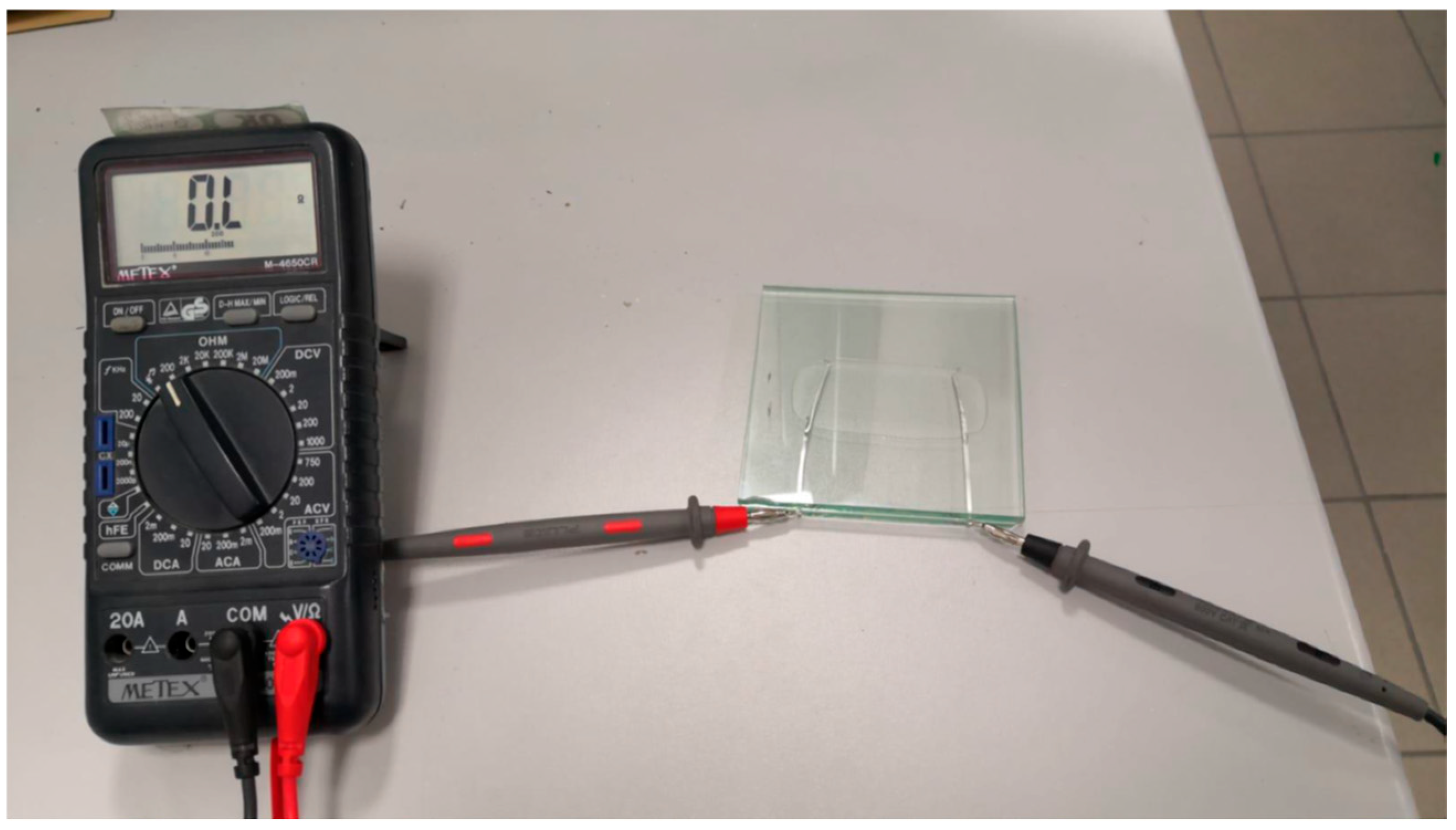
The sensor layer was made using the spray-coating method. The GO-hydrazine dispersion with the matrix was applied to a polymer (or quartz) substrate using an airbrush system with N2 as the carrier gas. N2 inlet pressure of two bar. The spray rate was 3 mL/min. The distance of the nozzle tip was kept from the ground to 12 cm. Spray deposition was performed by switching the N2 gas valve and the tank with the GO-hydrazine and cellulose dispersion sol. The created aerosol stream was directed onto a preheated substrate in the range of 20–30 °C. In order to ensure that the layer was made correctly, resistance measurement was carried out. The measurement was performed on the measurement set: power supply (P316 Meratronik, Wroclaw, Poland); digital multimeter (DT9207A Volt Kraft, Germany); and digital multimeter (EM391 EMOS, Przerow, Czech Republic). The produced layer has a resistance of 20 kOhm.
2.4. Preparation of Graphene-Based Inks
Graphene inks were prepared via a simple mechanical mixing method. Graphene-based inks include three main ingredients—dye, solvent, and binder. The dye is the most important ingredient, as it is responsible for the unique properties of the ink. In this case, we chose graphene flakes purchased from Sigma Aldrich. The inks prepared for this study were alcohol-based; for the solvent, we chose a mixture of toluene and ethanol in an 8:2 ratio. As graphene films on their own are fragile and easy to damage (unlike the GO films, which exhibit strong bonds within the layer), we decided to use ethyl cellulose as a film binder. As the ethyl cellulose is insulating, we kept its weight percentage to 2 wt%, which ensures the mechanical stability of a thin film while not deteriorating the conductivity of the as-prepared thin film.
2.5. Spray-Coating of Graphene Thin Films
The as-described graphene inks were used to fabricate thin films using the spray-coating method. The spray-coating set-up consisted of a commercially bought spray gun with a compressed air supply and a hotplate to preheat the substrates. The film deposition takes place as the spray gun moves over the substrate multiple times to ensure homogenous film formation. The thickness of a thin film can be controlled by changing the number of passes over the substrate surface.
2.6. Methods
PEDOT:PSS layers were deposited on a 5 cm × 2.5 cm glass substrate using the spin-coating method. The solution was spread on the slides and then centrifuged at a speed of 2500 rpm. The layers were dried at 150 °C for at least 4 h. After heating the manufactured layer at 150 °C, the layers were subjected to UV–Vis spectra analysis.
Transmission UV–Vis spectra of two GO layers with thicknesses of 10–20 and 50–100 μm were obtained using an A360 UV–Vis spectrophotometer (AOR Instruments, Shanghai, China) with an interval of 0.2 μm and a medium scanning speed.
Electrical measurements were performed with voltage polarization ranging from 0 to 10 V using a multi-channel potentiostat–galvanostat (PGStat Autolab M101, Metrohm, Barendrecht, The Nederland) connected to a computer. The experiment was designed to apply a voltage with 0.5 V steps between each step. The current response of the sample and the current flowing were recorded at three-minute intervals, with each step separated by a ten-second break.
SEM images were acquired using the Raith eLine+ system (Dortmund, Germany) with 10 kV gun tension.
2.7. The Concept of Placing the Sensor on the Photovoltaic Panel
The photovoltaic module equipped with a sensor is mounted on a sound-absorbing screen in the form of modules containing single photovoltaic cells (
Figure 2).
The photovoltaic panel with a mechanical damage sensor in the example is the first embodiment according to the invention made of a photovoltaic panel. It comprises a photovoltaic cell (1), which is covered from above and below (2), and an (3) ethylene–vinyl acetate (EVA). On the EVA (2) that covers the photovoltaic cell (1) from the top, there is tempered glass (4), which in turn is covered in self-cleaning coating (5). The developed PV module has a sensor that monitors mechanical damage to the protective glass. It takes the form of thin strips of graphene applied to the underside of the glass. The sensor (6) consists of two strips, with a thickness of 10 µm–100 µm, preferably 40 µm, and a width ranging from 3 to 8 mm, preferably 5 mm, which run along the entire length of the photovoltaic panel. The two sensor strips are located on the edges of the panel on both sides to increase the detection of damage on the panel surface. Their size is dictated by the available panel area with photovoltaic as well as electrical properties (of each strip), enabling reading of their changes after damage occurs. Thus, the exact length, width, and thickness of the coating of the electrical conductor are set to be based on ordinary resistance measurements made with a typical meter and their changes when a photovoltaic panel is damaged. Sensor 6 is intended to be applicable to photovoltaic panels of all known dimensions, with lengths of less than 1 m and more than 1 m.
Preferably, the graphene matrix is an amount of cellulose or polyvinylpyrrolidone 1÷5% by weight. The bottom of the sensor (6) is covered with EVA polymer (Film EVA9110T) (7). For each strip, a system is connected to the contacts formed at both ends, which continuously measures the resistance of each strip separately. Polymer foil (7) is used to tightly foil the internal layers of the panel to isolate them from unfavorable weather conditions—mainly moisture.
The sensor provides information about mechanical damage to a single PV cell or the entire set of cells in the photovoltaic module. The photovoltaic element itself has a layered structure produced by laminating the photovoltaic cell in a laminate layer based on EVA. Additionally, to protect the cell on the exposed side, tempered glass covered with a self-cleaning layer is installed (
Figure 2).
It is crucial that the sensor informs about the damage that affects the direct operation of the solar cell. Taking into account the method of construction of the photovoltaic element, it is proposed to place the sensor on the surface:
EVA top laminate on the surface facing the photovoltaic cell;
EVA top laminate on the tempered glass side;
tempered glass, EVA laminate on the surface;
tempered glass between the glass and the self-cleaning surface.
However, due to the construction of the PV module, the best location for placing the sensor is the underside of the tempered glass. In this position, the sensor is directly on the glass, protected from external factors. Additionally, implementing it on the glass is much simpler and more reliable than on the surface of EVA.
Photovoltaic parameters of the constructed PV panel (without sensor) were determined using a measuring system equipped with a Solar System for Solar Cells Characterisation manufactured by PV Test Solutions, Wrocław, Poland (The system includes: solar radiation simulator of AAA class, model SS200AAA EM and measurement system SS I–V CT-02 with PV Test Solutions software Solar Cell Tester v.2.8.0.5). Basic electrical parameters are given in
Table 2.
The dimensions of the complete module are 1810 mm × 2200 mm. The dimensions of a single submodule are 1640 mm × 190 mm. The module consists of 6 submodules that are arranged parallel with a gap of 210 mm. Installing a sensor on the PV panel did not change the photovoltaic parameters of the panel.
3. Results
The main goal of this work was to connect the photovoltaic panel with a sensor towards continuous and maintenance-free monitoring of the set of PV panels for their mechanical damage and enable quick location. The selection of appropriate materials and the design of both devices are important for efficient functioning. The sensor should have low mechanical resistance, interrupt the conductive path in the event of a crack in the monitored surface and an appropriately high resistance and, at an appropriate level, the measurable value of its change when the circuit is damaged. A photovoltaic panel has a mechanical damage sensor in which the photovoltaic panel is made of a photovoltaic cell, covered on the top and bottom foil. Placed on the foil that covers the photovoltaic cell from above is tempered glass, which in turn is covered with a self-cleaning coating.
Our idea is characterized by equipment with a sensor for monitoring mechanical damage, which takes the form of damage applied to the photovoltaic panel containing at least one strip which is made of an electrical conductor in the form of graphene coatings— graphene flakes in a matrix or graphene oxide in a matrix warp. Preferably, the sensor is placed on the cell covering the bottom photovoltaic panel.
3.1. The Concept of the Sensor System and Structure
We propose to make the sensor a thin electrically conductive layer based on graphene or a conductive polymer such as PEDOT:PSS. It is proposed to create a layer that provides information about mechanical damage to the cell based on a decrease in the flow of electric current (increase in resistance). It is therefore reasonable to cover as much of the cell surface as possible with a sensor layer. Still, it may have a significant impact on the lamination process during cell encapsulation. To minimize the effect of the conductive layer on the adhesion processes of individual layers during lamination, it is proposed to create narrow conductive paths that have their electrical characteristics. Information about cell damage is a change in these electrical characteristics. The proposed materials have significantly lower electrical conductivity. Moreover, their unique feature is the ability to transmit light in a wide visible range of light. It is suggested that the sensor elements be made directly above the cell, while the remaining conductive paths collecting the electrical signal from the sensor are based on standard metallic connections. In this system, the largest contribution to the electrical signal comes from the transparent element of the sensor.
It is advantageous of our paper that the application of tested materials can be performed through various methods, including spin-coating, spray-coating, and doctor blade, and consequently the sensor is manufactured in the form of a thin coating, obtained through the produced layer of graphene flake or graphene oxide in a warp. The solution allows for use in any atmospheric conditions and can be used inside and outside buildings, both industrial and residential. The use of graphene or graphene oxide, due to high resistivity and the value of its change at the appropriate height level in the event of damage to the measuring circuit, allows for diagnosis of the system in terms of evaluation zero–one, where one means that the system is operational and zero means that the system is damaged. It should be stressed that in our work, an important element is the reduction process to produce a reduced form of graphene oxide. The reduction process slightly changes color to a darker one and significantly improves the material’s conductive properties.
3.2. UV–Vis of Graphene in Oxidized Form and PEDOT:PSS
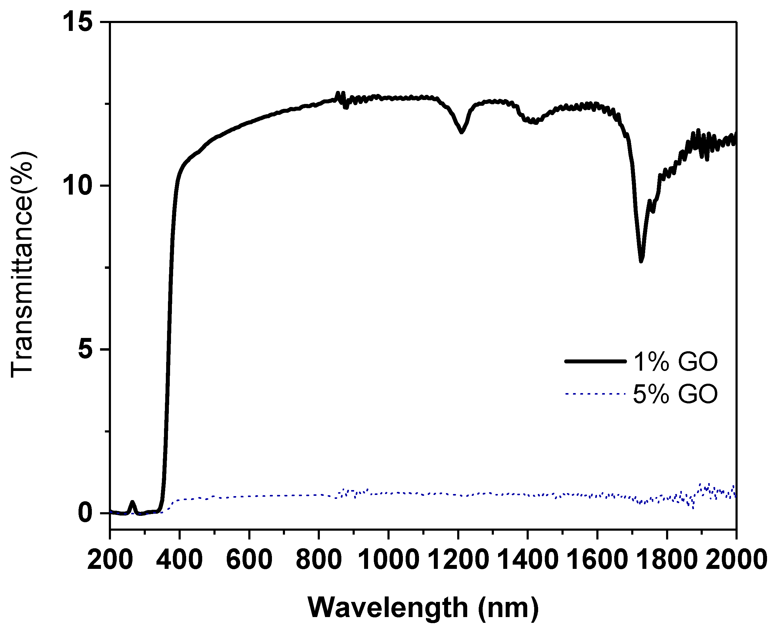
Graphene or graphene oxide (GO) can be deposited from an aqueous solution in the mold a suspension containing from 2 to 4%, preferably 3% by weight of graphene/graphene oxide. Due to their structure, graphene and graphene oxide ensure very good adhesion of the compound to the surface. Graphene or graphene oxide, after application and when dry, forms thin layers that adhere very well to the substrate. In the first stage of our work, the UV–Vis optical properties of thin graphene oxide layers on the EVA laminate were performed.
Two GO layers with thickness 10–20 μm and 50–100 μm were investigated by UV–Vis spectroscopy. Our research showed that the UV–Vis spectrum of both GO layers did not show absorption bands in the range of 350–800 nm similar to the EVA laminate itself, which proves that the GO layer should not affect the investigated light absorption in the range important for solar cells. The presence of an additional one layer did not change the absorption of the laminate itself.
All PEDOT:PSS layers showed very similar spectral characteristics, regardless of the one used starting solution. In terms of absorption, neither layer absorbs in the key range for a solar cell.
3.3. Electrical Properties of PEDOT:PSS
To test the conductive properties of PEDOT:PSS compounds, four polymers (with different ratios of PEDOT to PSS) were selected (see Experimental part). Electrical properties of PEDOT:PSS layers were performed with voltage polarization ranging from 0 to 10 V using a multi-channel potentiostat–galvanostat. Unfortunately, for the PEDOT:PSS layers with continuous dimensions of 2.5 cm × 5 cm, the resistance values for current flow along the layer exceeded 100 GOhm, making it impossible to observe the current flow. In the next stage, samples with an optimized arrangement of conductive bands were made. Subsequent modifications to the design of the sensor layer led to a satisfactory drop in resistance in the pots. The final layer has a resistance of 20 kOhm.
3.4. Technological Solutions for the Sensor Design
As part of the development work, the task was carried out in the form of two potential technological solutions for the production of sensor coatings:
- ➢
monolayer (two-layer) of graphene obtained by epitaxy;
- ➢
multilayer coating of flake graphene, obtained by applying a GO layer, then reducing it or applying a GO layer in the matrix.
The development of a sensor based on layered graphene deposited by epitaxy is already known from our previous publication [
40]. The procedure described therein was adapted to constructing photovoltaic panels combined with acoustic screens. However, when analyzing the cost of a mono-layer with an area of 50 × 50 cm, it turned out that the commercial use of such a layer is not economically justified. The profit/cost analysis eliminated the validity of this solution in practice. Therefore, it seems that the use of this solution on a large scale is still unjustified (mainly due to costs), most likely until mass production of graphene mono-layers begins.
Consequently, in the next step of our work based on the developed coating preparation technologies, two types of sensor design solutions were proposed and constructed:
- ➢
Sensor based on an oxidized form of graphene flake (GO-flakes);
- ➢
Sensor based on an oxidized form of graphene flake (GO-flakes) in the matrix.
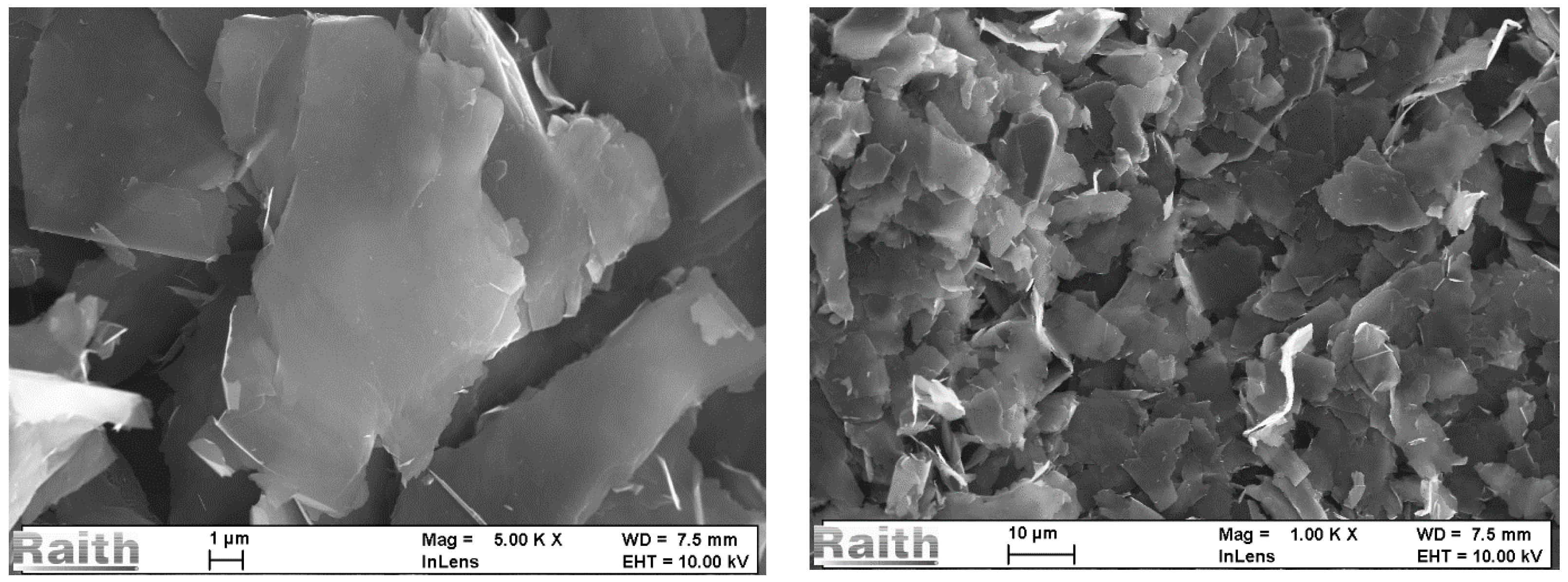
The morphology of GO-flake samples was determined by scanning electron microscope (SEM) imaging.
Figure 3 shows the distribution of a few microns in lateral size of GO-flakes in the film. The flakes are composed of a few-layered graphene structures and tend to agglomerate with the film structures. Images were acquired at 1 kX and 5 kX magnification. The working distance was approximately 10 mm at high vacuum mode with 10 kV.
3.5. Sensor Based on the Oxidized Form of Graphene Flake
This solution involves applying a layer of GO-flake onto a flexible EVA layer and then reducing it at a temperature above 200 °C to GO. It was intended to be used after applying it to a photovoltaic panel from the side of the incident light, mainly due to the slight loss of transparency of the layer. However, when transparency is maintained at the level of 95%, the conductivity of the layer is undetectable (see
Figure 4), probably because the layer is too thin.
3.6. Sensor Based on Oxidized Form of Graphene Flake in the Cellulose Matrix
With reference to the results of the tests obtained above, we propose using a GO-flake layer placed in a matrix on a flexible EVA layer. The matrix is cellulose in which GO-flake with an amount of 1÷5% by weight is placed. This type of layer has a resistance of 20 kOhm. The limitation of using this solution to examine damage from the side of the light dropping on the photovoltaic panel is the (significant) loss of transparency of the layer. Unfortunately, a loss of transparency of 95% of the conductive layer was observed (
Figure 5). For this reason, this solution is proposed to be used from the inside of the photovoltaic panel. The strong peak at ~1700 cm
−1 is due to the ketone group. The weakness deep at ~1400 cm
−1 corresponds to the stretching of the sulfonate group, and the one at ~1200 cm
−1 is related to the presence of carbonyl groups.
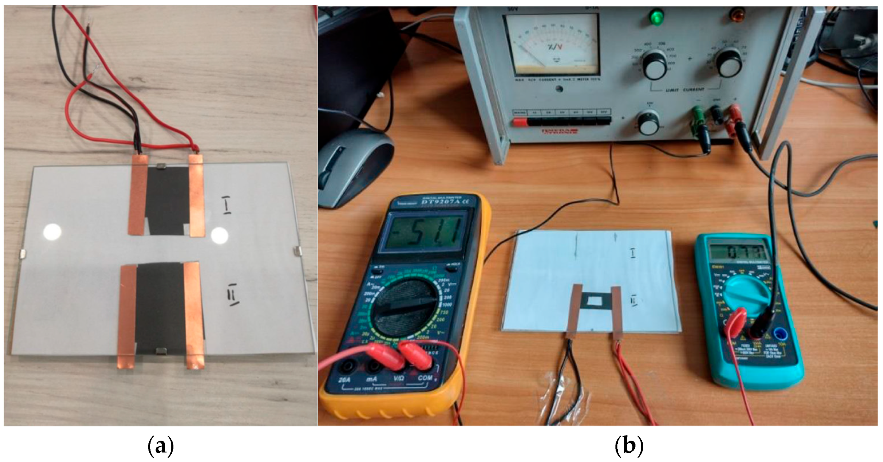
Finally, we investigate the electrical properties of the constructed sensor based on the oxidized form of graphene flake (GO-flake) in the cellulose matrix with a concentration of 1% and 5% by weight. They are placed, for measurement, between two glass plates.
Figure 6b shows the measurement station used to determine the resistance of appropriate layers.
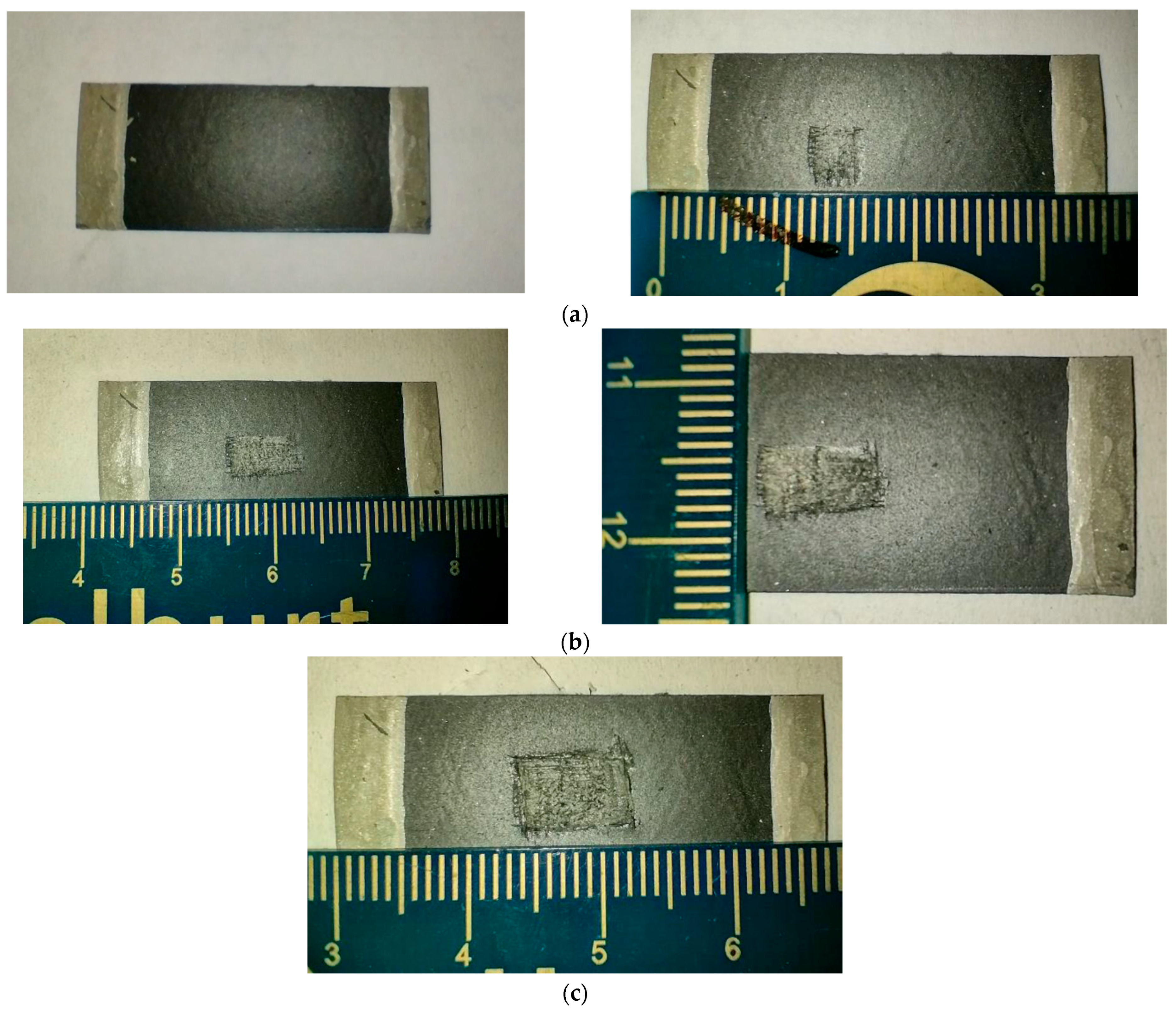
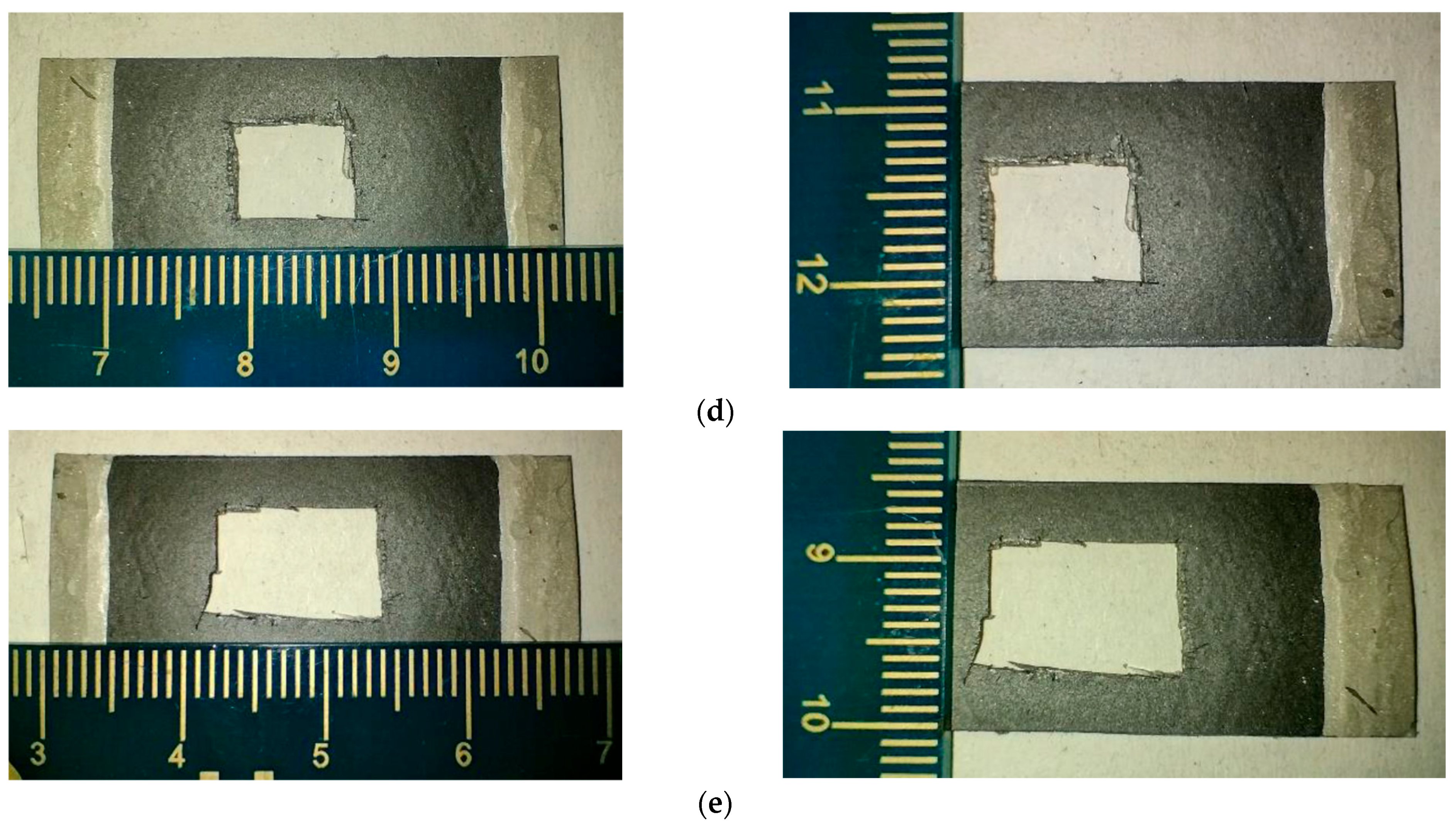
In order to ensure the sensor’s response in the zero-to-one range, where zero means no damage to the PV panel and a unit value means damage, a test was carried out on a GO-flake layer in a cellulose matrix with dimensions of 16 mm × 28 mm. The reference sample (
Figure 7a) was damaged in five different ways.
- ➢
Hole No. 1 is a surface damage in the form of a scratch with a uniform ratio of height to length of damage 4 mm × 4 mm (
Figure 7a).
- ➢
Hole No. 2 is a surface damage in the form of scratching with a varying ratio of height to length of damage 5 mm × 8 mm (
Figure 7b).
- ➢
Hole No. 3 is a deep damage that involves cutting the structure of the layer along the outline of the hole without removing the interior. A hole with a different ratio of height to length of damage 5 mm × 8 mm (
Figure 7c).
- ➢
Hole No. 4 is a deep damage consisting of cutting the layer’s structure along the outline of the hole and removing the interior. A hole with a different ratio of height to length of damage, 6 mm × 8 mm (
Figure 7d).
- ➢
Hole No. 5 is a deep damage consisting in cutting the structure of the layer along the outline of the hole with the removal of the interior, but with a larger hole area than Hole No. 4. Hole No. 5 varies in the ratio of the height to the length of the damage and is 8 mm × 13 mm (
Figure 7e).
Figure 7.
(a) The sensor is undamaged (reference sample R). The GO-flake layer in the cellulose matrix has dimensions of 1.6 cm × 2.7 cm (left side). Sensor damaged: Hole no. 1 scratched 4 mm × 4 mm (right side); (b) Sensor damaged: Hole no. 2 scratched 5 mm × 8 mm; (c) Sensor damaged: Hole no. 3 cut out 5 mm × 8 mm; (d) Sensor damaged: Hole no. 4 cut out 6 mm × 8 mm; (e) Sensor damaged: Hole no. 5 cut out 8 mm × 13 mm.
Moreover,
Figure 8 summarizes the results of resistance measurements of GO-flake layers in the cover with appropriate types of damage.
Table 3 summarize the results of resistance measurements of GO-flake layers in the cover with appropriate types of damage.
4. Discussion
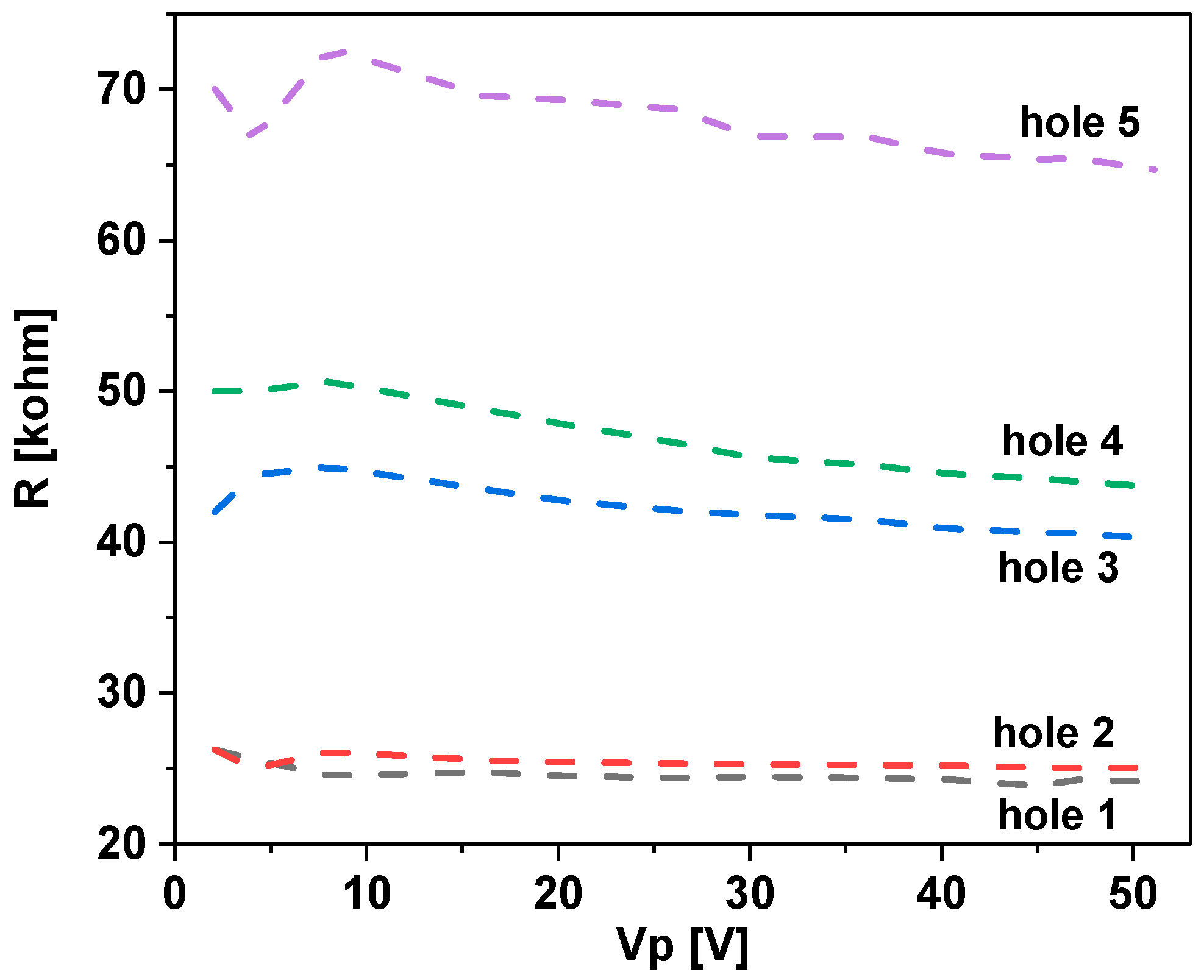
Two systems of causing damage to the sensor were constructed, first by repetitive scratching in the given dimensions (4 × 4 and 5 × 8 [mm × mm]) and second by cutting out the given area (5 × 8, 6 × 8 and 8 × 13 [mm × mm]). In this experiment, to examine the behavioural changes caused by inflicted damage for applied potential in the range from 2.1 to 51.1 V, current response was registered allowing calculation of the total resistance of the sensor. It was easy to notice the basic difference between the scratched surface area and the cut-out one; the registered resistance oscillated between 25 and 26 Ω, whereas the cut surface showed values more than 1.5 times higher. The difference obtained by cutting out showed increasing resistance upon increasing the size of missing part, whereas the scratched surfaces did not differ very much.
Figure 8 shows that even slight damage or scratch to the sensor allows for reading its resistance changes. This proves the high sensitivity of the sensor based on graphene in a cellulose matrix. Moreover,
Figure 8 shows the change in sensor resistance resulting from the change in its surface due to damage changes by 9.3%, 11.1%, and 24.1% for individual holes, respectively. The sensor surface due to damage can therefore be monitored through measurable changes in its resistance value. The mechanism may consist of surface structure changes (sample without a hole) where scratches affect only the surface. This causes changes in the volume of the conductive material, which are sufficient to detect this type of damage. Changes consisting of material disruption (sample with holes) also affect the volume of the conductive material (sample). Despite this, linear changes in conductivity are not observed throughout the sample. In comparison, materials with significantly higher conductivity values have a sensitivity threshold at significantly larger damage sizes. This may suggest the formation of surface conductivity in the tested samples, the changes in which, through the defect, affect the global value of resistance. This may not be observed in samples with holes as defects. The proposed architecture of the sensor can be used in laboratory and field conditions. Even two years after the last experiment, the presented samples are still sensitive and provide the same results. There are no external factors observed that change the properties of the material/samples.
Before conclusions, we add that advanced materials as a source of new technologies are also used by the Armed Forces, improve situational awareness, command and control, and communication, and they have a crucial role in the success on the battlefield. In military operations, systems consisting of all types of sensors provide the necessary data to evaluate or optimize the decision-making process. Current research on weapon systems and military devices is the battlefield’s future [
41]. Modern military systems are used on the line of contact with the enemy, urban fighting, rear areas, and combat support and can also be used in situations other than war, e.g., in crisis response management or to protect critical infrastructure. All systems using infrared, laser, or acoustic waves are used to carry out the above tasks. During military operations near or in cities where plants with hazardous materials, chemical, biological, radioactive, and explosive sensors are used to monitor the changing situation [
42]. Effective implementation of combat tasks requires communication that ensures delivering information between the superior and the subordinate. Military strategy and combat operations have changed significantly since the end of the twentieth century. Modern communications with data transmission, which are interconnected and able to communicate with each other, have affected the speed of information transfer. It is crucial during the performance of combat tasks at every stage, from planning, giving orders, and ending on realization. Communication is usually limited to a specific zone and time but must be used when necessary [
42]. Remote nodes with special prosperities are used for communication, which requires power supplies. The use of photovoltaic panels with energy storage will allow for an independent power source.


 ,
, 
