
Reliability Analysis of Transient Voltage Suppression Diodes Under Direct Current Switching Surge Stress


Abstract
1. Introduction
Focus and Outline of This Study
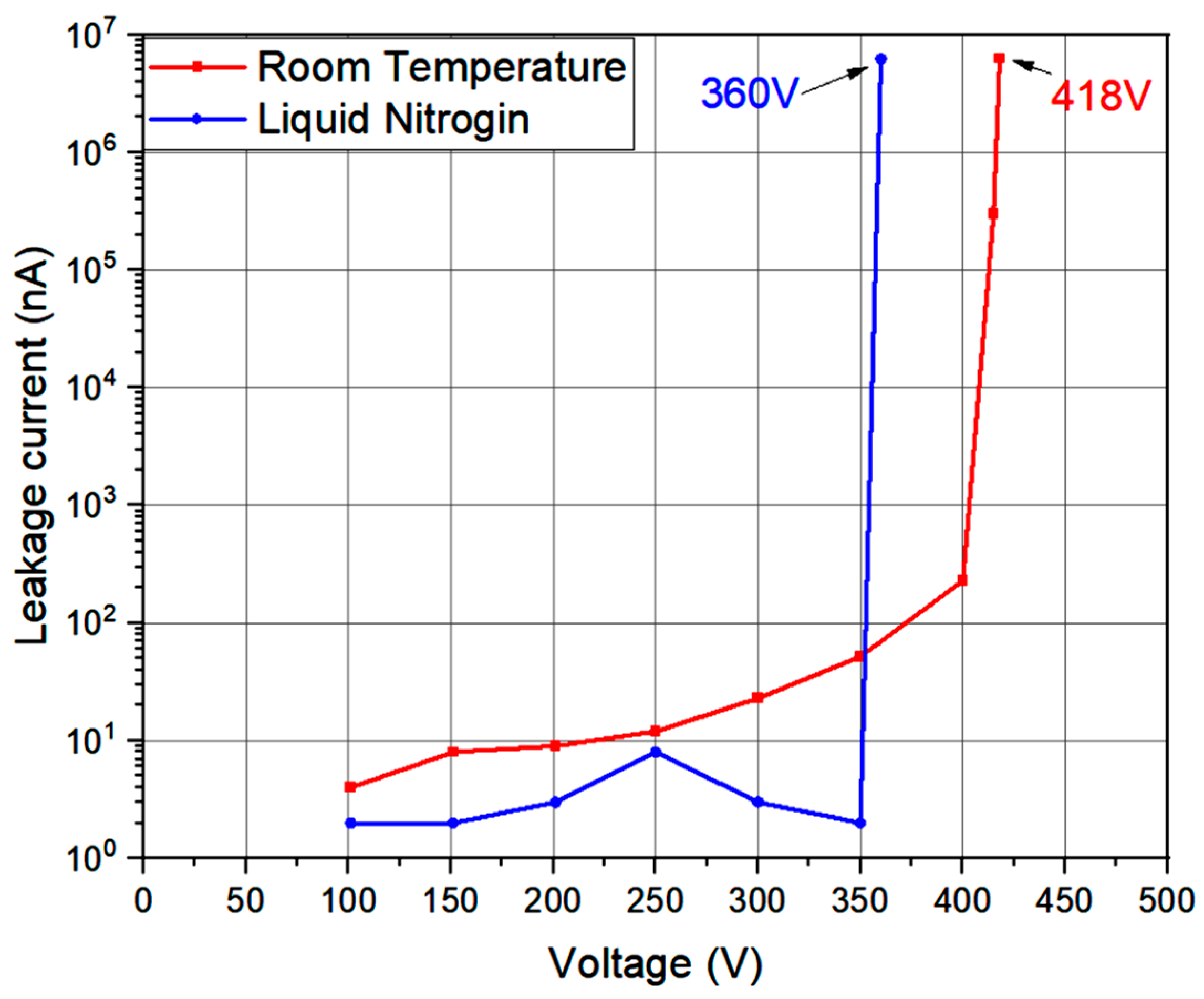
2. Literature Study
- A TVS diode with a graded P-N junction (G-TVSD);
- A TVS diode with a shorted P-N junction in the cathode region (PG TVSD);
- A TVS diode with trench P+ doping connected in the cathode region (TG-TVSD);
- A TVSD with a local Schottky contact (STG-TVSD);
- A TVSD with a lightly doped N-Drift at the cathode (LSTG-TVSD).
- TVS diodes are used for electrostatic discharge applications;
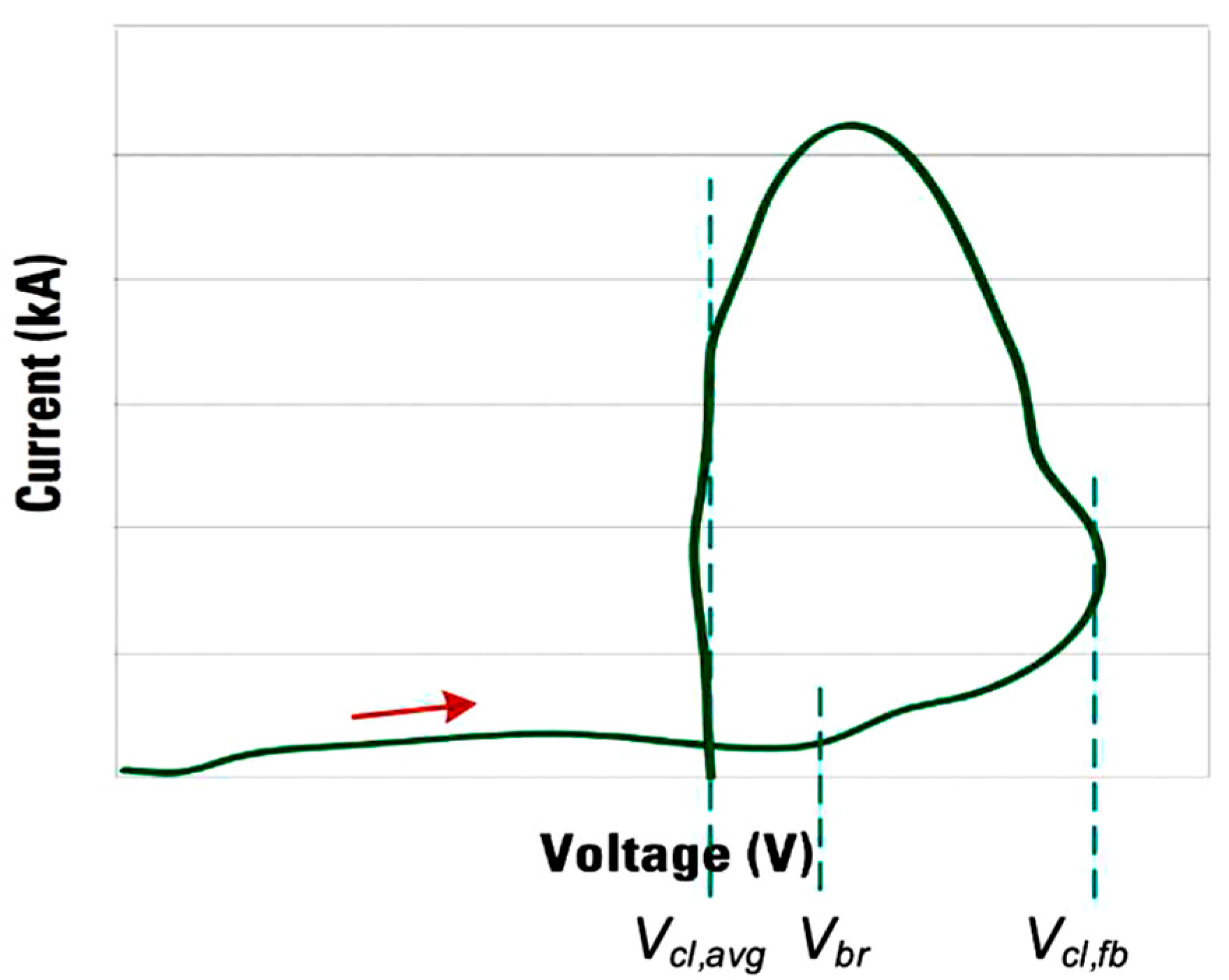
- The voltage level when the TVS diode starts to clamp is the VBR or VC;
- VC should be lower than the maximum expected surge voltage to ensure protection;
- TVS exhibits a lower VC compared to MOVs; therefore, it can be used together with semiconductors that have lower breakdown collector–emitter voltages;
- When the biasing voltage level is above VBR, usually defined at IR = 1 mA or IR = 10 mA, the TVS enters avalanche mode. IR will then increase exponentially;
- They offer low electromagnetic interference (EMI) due to intrinsic capacitance values;
- In the work of [4], the Cassie–Mayr black box model has been developed to analyse switching transients in low-voltage circuits during current interruptions. The switching overvoltage that is produced above the peak voltage during current interruption is limited by TVS diodes.
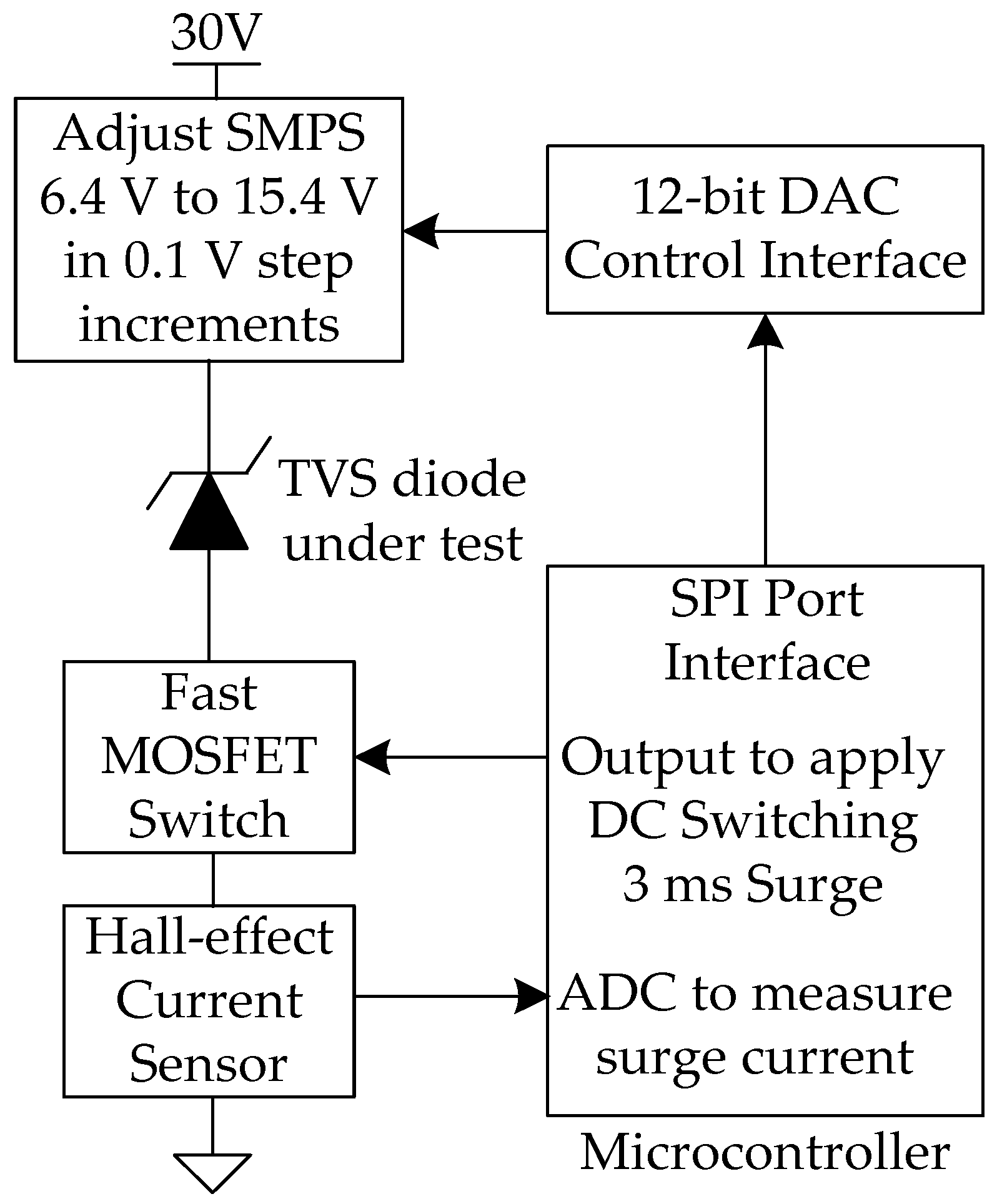
3. Methodology
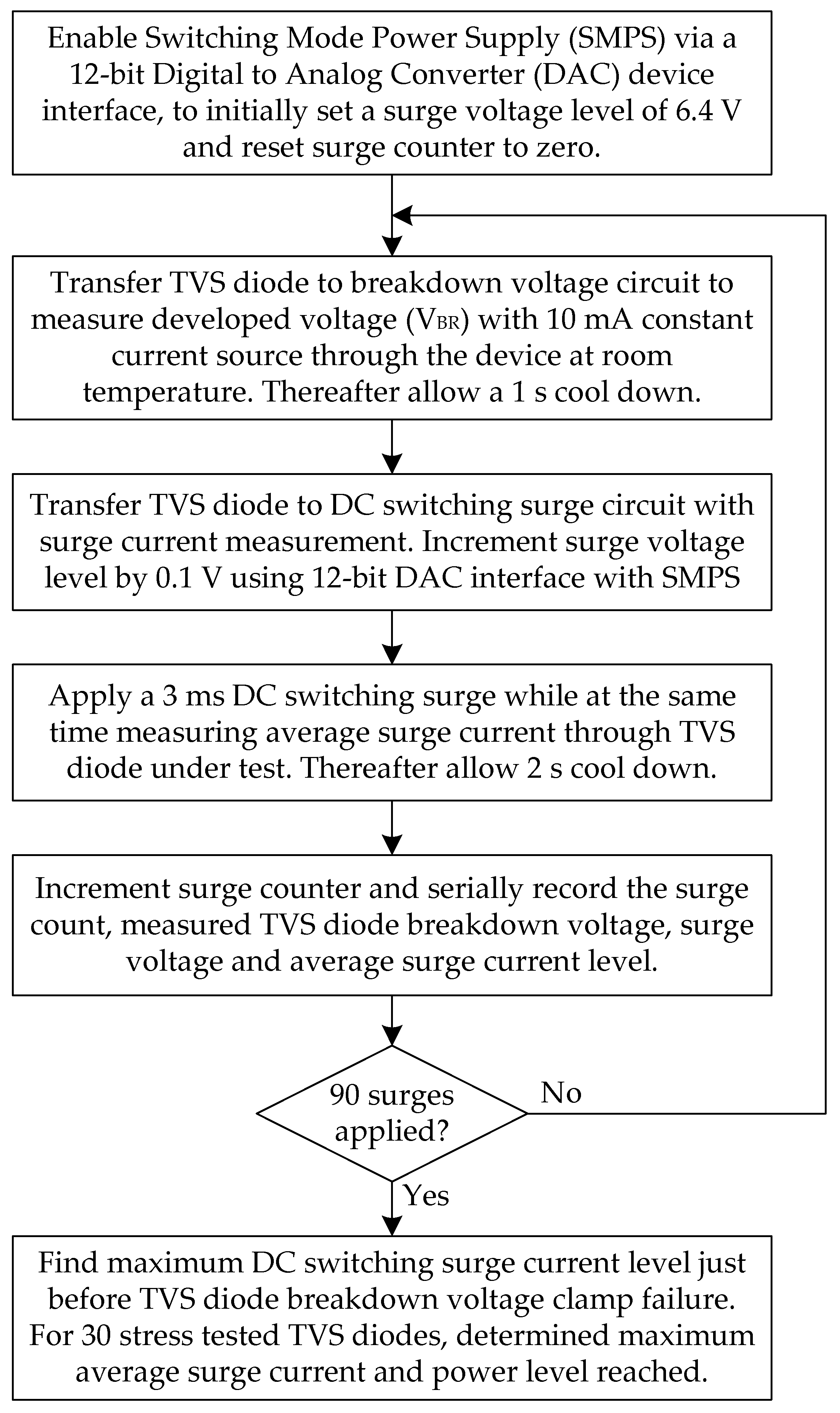
3.1. Surge Voltage Level Adjustment
3.2. TVS Diode Breakdown Voltage Measurement
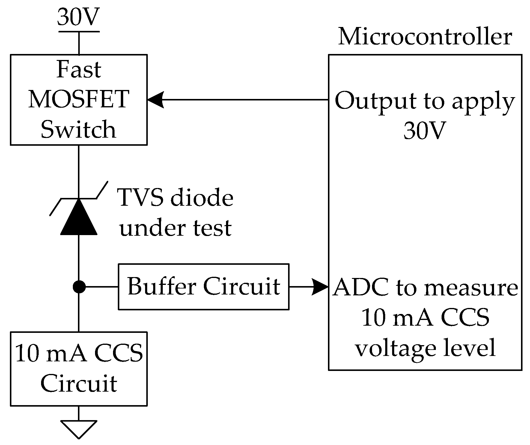
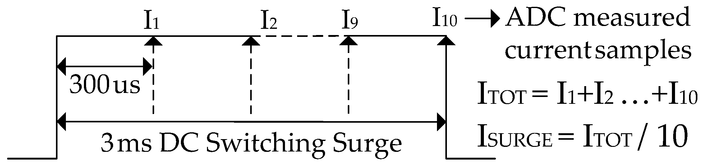
3.3. DC Switching Surge Current Measurement
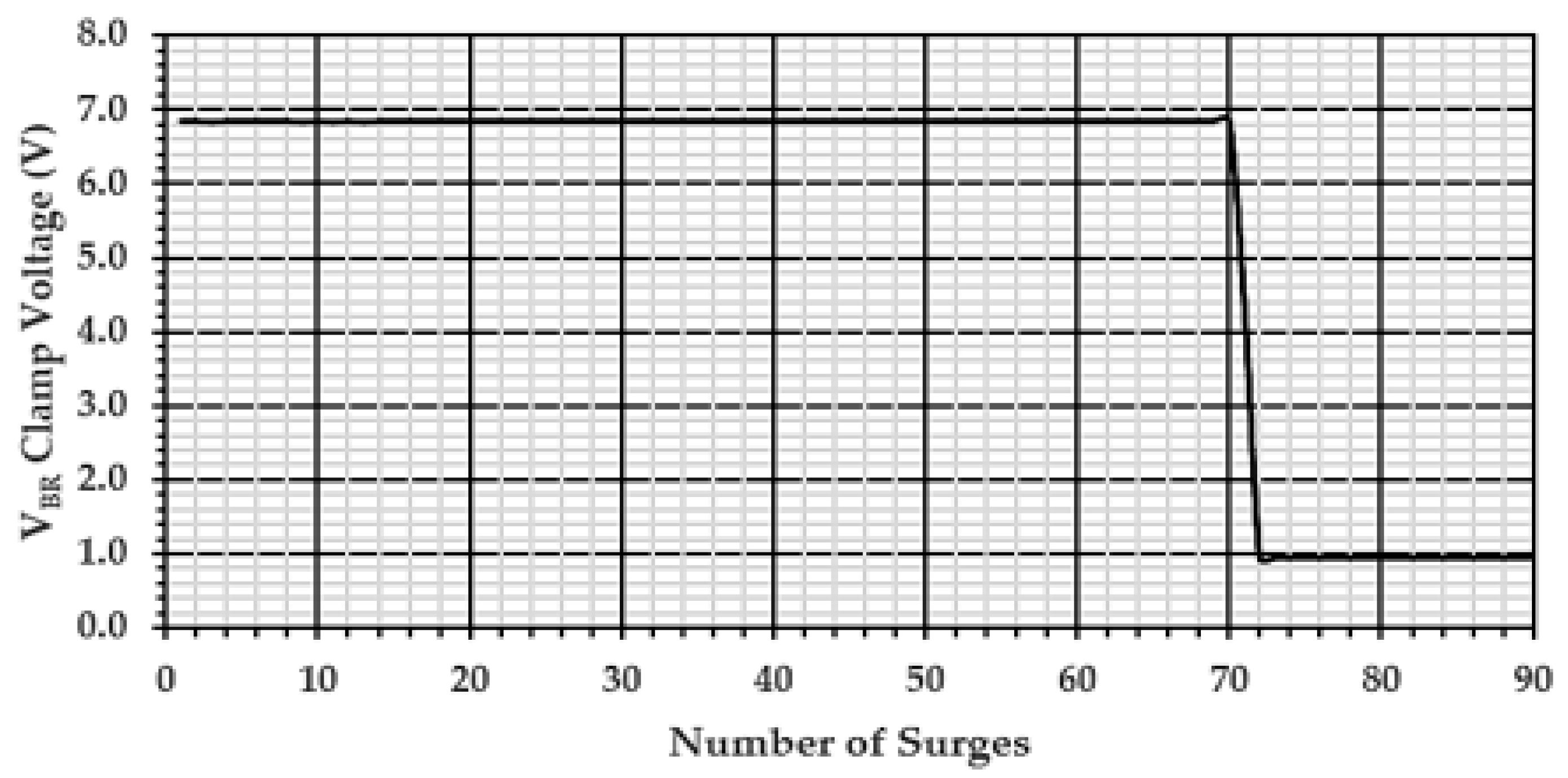
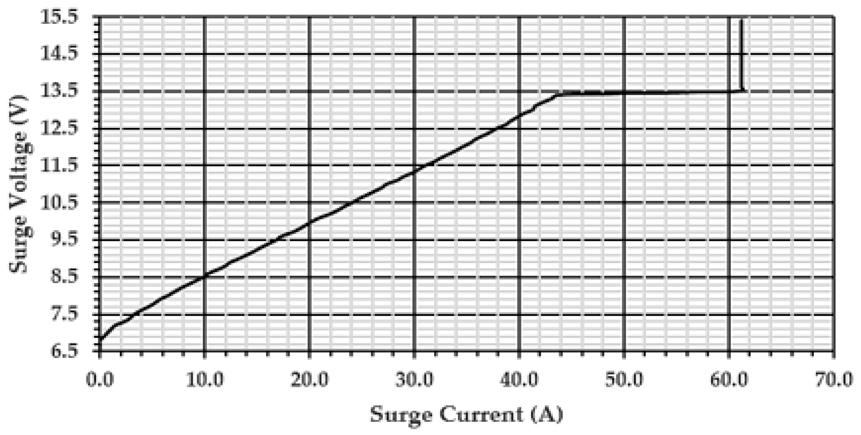
4. Results and Discussion
4.1. TVS Diode Measured Sample Data Summary
4.2. TVS Diode Calculated Confidence Intervals
5. Conclusions
Author Contributions
Funding
Data Availability Statement
Conflicts of Interest
Abbreviations
| AC | Alternating current |
| ADC | Analogue-to-digital conversion |
| CCS | Constant current source |
| DAC | Digital-to-analogue converter |
| DC | Direct current |
| DFSS | Design for Six Sigma |
| DMADV | Define, Measure, Analyse, Design and Verify |
| EMI | Electromagnetic interference |
| ESD | Electrostatic discharge |
| IC | Integrated circuit |
| IO | Input/output |
| IQR | Interquartile range |
| LOC | Level of confidence |
| LOS | Level of significance |
| LSB | Least significant bit |
| MOV | Metal oxide varistors |
| MOSFET | Metal–oxide–-semiconductor field-effect transistor |
| SEED | System-Efficient Electrostatic Discharged |
| SMPS | Switched mode power supply |
| SPI | Serial port interface |
| TVS | Transient voltage suppression |
References
- Magnusson, J.; Saers, R.; Liljestrand, L.; Engdahl, G. Separation of Energy Absorption and Overvoltage Protection in Solid-State Breakers by the Use of Parallel Varistors. IEEE Trans. Power Electron. 2014, 29, 2715–2722. [Google Scholar] [CrossRef]
- Sande, R.; Leibfried, T. Considerations on Energy Absorption of HVDC Circuit Breakers. In Proceedings of the 49th International Universities Power Engineering Conference (UPEC), Cluj-Napoca, Romania, 2–5 September 2014; pp. 1–6. [Google Scholar] [CrossRef]
- Liu, J.; Zhang, G.; Chen, Q.; Qi, L.; Qin, Z.; Wang, J. Research on Dynamic Modeling and Transient Characteristics of Hybrid DC Switch. In Proceedings of the 1st International Conference on Electrical Materials and Power Equipment (ICEMPE), Xi’an, China, 14–17 May 2017. [Google Scholar]
- IEEE Std C62.11-2012 (Revision of IEEE Std C62.11-2005); IEEE Standard for Metal-Oxide Surge Arresters for AC Power Circuits (>1 KV). IEEE: Piscataway, NJ, USA, 2012.
- Woodworth, J.J.; Comber, M.G. Improvements in IEEE C62.11 test standards. In Proceedings of the PES T&D 2012, Orlando, FL, USA, 7–10 May 2012; pp. 1–7. [Google Scholar] [CrossRef]
- van Niekerk, D.; Bokoro, P. A Durability Model for Analysis of Switching Direct Current Surge Degradation of Metal Oxide Varistors. Electronics 2022, 11, 1329. [Google Scholar] [CrossRef]
- Zhang, C.-R.; Zeng, X.; Zhou, L.; Mao, J.-F. Protection Effects Using Transient Voltage Suppressor Diodes Based Circuits Under High-Power Microwave Pulses. IEEE Trans. Electromagn. Compat. 2021, 63, 2058–2064. [Google Scholar]
- Bento, A.R.F.; Bento, F.; Cardoso, A.J.M. A Novel DC Circuit Breaker with an Absorbing Branch Based on TVS Diodes. In Proceedings of the 2023 IEEE Fifth International Conference on DC Microgrids (ICDCM), Auckland, NZ, USA, 15–17 November 2023; pp. 1–5. [Google Scholar] [CrossRef]
- Liu, C.; Kong, M.; Chen, H.; Yi, B.; Zhang, B.; Chen, X. Simulation Study on Novel High Voltage Transient Voltage Suppression Diodes. In Proceedings of the 2019 IEEE 13th International Conference on ASIC (ASICON), Chongqing, China, 29 October–1 November 2019. [Google Scholar] [CrossRef]
- Oramus, P.; Chmielewski, T.; Kuczek, T.; Florkowski, M. Application of Bidirectional Transient Voltage Suppressor for Electric Arc Suppression in LV Switches—Simulation and Laboratory Case Study. In Proceedings of the 2017 Progress in Applied Electrical Engineering (PAEE), Koscielisko, Poland, 25–30 June 2017. [Google Scholar] [CrossRef]
- Ravi, L.; Liu, J.; Dong, D.; Burgos, R.; Song, X.; Cairoli, P. TVS Diode Coupled Gate Driver Circuit for Series Connected Power Devices used in Circuit Breaker Applications. In Proceedings of the IECON 2021—47th Annual Conference of the IEEE Industrial Electronics Society, Toronto, ON, Canada, 13–16 October 2021; pp. 1–6. [Google Scholar]
- Khodadadian, E.Z.; Joodaki, M. Decreasing the Loading Effect of the TVS Diode Using a Transmission Line for RF and Microwave Applications. IEEE Lett. Electromagn. Compat. Pract. Appl. 2021, 3, 29–33. [Google Scholar] [CrossRef]
- Yoshida, T.; Endo, M. A Study on ESD Protection Characteristic Difference Measurement of TVS Diodes by VNA. In Proceedings of the 2017 IEEE 5th International Symposium on Electromagnetic Compatibility (EMC-Beijing), Beijing, China, 28–31 October 2017; pp. 1–4. [Google Scholar] [CrossRef]
- Wang, Z.; Zeng, X.; Deriszadeh, A.; Nilsson, E.; Rouquette, J.F.; Surapaneni, R.K.; Galla, G.; Ybanez, L.; Pei, X. Performance of Snubber Capacitors and TVS Diodes for Cryogenic Power Electronics. In Proceedings of the 2023 IEEE Energy Conversion Congress and Exposition (ECCE), Nashville, TN, USA, 29 October–2 November 2023; pp. 1774–1780. [Google Scholar] [CrossRef]
- Dai, S.-H.; Wang, H.-N.; Chiang, M.-T.; Lin, C.-J.; King, Y.-C. Leakage Suppression of Low Voltage Transient Voltage Suppressor. In Proceedings of the 2007 45th Annual IEEE International Reliability Physics Symposium, Phoenix, AZ, USA, 15–19 April 2007; pp. 592–593. [Google Scholar] [CrossRef]
- Meier, F. Design of transient voltage suppressors for digital inputs of avionics devices in indirect lightning tests according to ED–14/DO–160. In Proceedings of the 2013 International Symposium on Electromagnetic Compatibility, Brugge, Belgium, 2–6 September 2013; pp. 833–836. [Google Scholar]
- Le, T.L.; Youssef, T.; Azzopardi, S.; Lebey, T.; Lasserre, P.; Bruder, A.; Lefebvre, B. Solid-state Circuit Breaker for aircraft high voltage DC network. In Proceedings of the 2024 IEEE Applied Power Electronics Conference and Exposition (APEC), Long Beach, CA, USA, 25–29 February 2024; pp. 3100–3107. [Google Scholar]
- Staikos, E.T.; Hadjicostas, A.Y.; Peppas, G.D.; Tsovilis, T.E. Coordination of Varistors With Transient Voltage Suppression Diodes in Automotive DC Systems. IEEE Trans. Veh. Technol. 2024, 73, 450–462. [Google Scholar] [CrossRef]
- Zhou, J.; Xu, Y.; Bub, S.; Holland, S.; Meiguni, J.S.; Pommerenke, D.; Beetner, D.G. Transient Response of ESD Protection Devices for a High-Speed I/O Interface. IEEE Trans. Electromagn. Compat. 2022, 64, 907–914. [Google Scholar] [CrossRef]
- Ravi, L.; Zhang, D.; Qin, Z.; Zhang, Z.; Xu, Y.; Dong, D. Electronic MOV-Based Voltage Clamping Circuit for DC Solid-State Circuit Breaker Applications. IEEE Trans. Power Electron. 2022, 37, 7. [Google Scholar] [CrossRef]
- Malabanan, F.; Abu, P.A.; Oppus, C.; Reyes, R. Design of an Interface Test Adapter for Sequential Testing of Transient Voltage Suppressor Diodes to Reduce Test Cycle Time. In Proceedings of the 2022 8th International Conference on Automation, Robotics and Applications, Prague, Czech Republic, 18–20 February 2022; pp. 176–180. [Google Scholar] [CrossRef]
- Zhang, Y.; Xu, S.; Song, Y.; Qi, W.; Guo, Q.; Li, X.; Kong, L.; Chen, J. Real-Time Global Optimal Energy Management Strategy for Connected PHEVs Based on Traffic Flow Information. IEEE Trans. Intell. Transp. Syst. 2024, 25, 20032–20042. [Google Scholar] [CrossRef]
- van Niekerk, D.; Venter, J. Experimental Approach for Reliability Analysis of Medium-Power Zener Diodes under DC Switching Surge Degradation. Electronics 2024, 13, 1976. [Google Scholar] [CrossRef]
- Zhou, L.; Zhang, S.; Yin, W.-Y.; Mao, J.-F. Immunity Analysis and Experimental Investigation of a Low-Noise Amplifier Using a Transient Voltage Suppressor Diode Under Direct Current Injection of HPM Pulses. IEEE Trans. Electromagn. Compat. 2014, 56, 1715–1718. [Google Scholar] [CrossRef]
- IEEE Std C62.33-2016; IEEE Standard for Test Methods and Performance Values for Metal-Oxide Varistor Surge Protective Components. IEEE: Piscataway, NJ, USA, 2018. [CrossRef]
- Shayib, M.A. Applied Statistics. 2016. Available online: https://oerstatistics.wordpress.com/wp-content/uploads/2016/03/applied-statistics.pdf (accessed on 25 March 2025).
- Ross, S. Introduction to Probability and Statistics for Engineers and Scientists, 4th ed.; Elsevier Academic Press: Burlington, VT, USA, 2009; pp. 242–454. [Google Scholar]


| Parameter | Specification |
|---|---|
| Peak Pulse Power Dissipation by 10/1000 μs waveform (Pppm) | 600 W |
| Peak Forward Surge Current by 8.3 ms single sine-wave (IFSM) | 100 A |
| Steady State Power Dissipation (PD) | 5 W |
| Breakdown Voltage (VBR) | 6.8 V |
| Manufacturer: | AB | CD | EF | ||||||
|---|---|---|---|---|---|---|---|---|---|
| Measured: | |||||||||
| Minimum | 6.90 | 25.7 | 178 | 6.76 | 43.6 | 297 | 6.84 | 47.7 | 327 |
| Quartile Q1 | 6.93 | 27.9 | 194 | 6.83 | 45.9 | 315 | 6.87 | 50.3 | 347 |
| Median Q2 | 6.93 | 28.7 | 199 | 6.84 | 47.2 | 323 | 6.90 | 51.6 | 355 |
| Quartile Q3 | 6.96 | 29.7 | 207 | 6.87 | 48.1 | 329 | 6.92 | 53.6 | 368 |
| Maximum | 6.99 | 32.4 | 220 | 6.90 | 50.2 | 343 | 6.96 | 56.1 | 384 |
| IQR = (Q3 − Q1) | 0.03 | 1.8 | 13 | 0.04 | 2.2 | 14 | 0.05 | 3.3 | 21 |
| Q1 − (IQR × 1.5) | 6.89 | 25.1 | 175 | 6.76 | 42.6 | 293 | 6.79 | 45.4 | 316 |
| Q3 + (IQR × 1.5) | 7.01 | 32.5 | 225 | 6.94 | 51.4 | 351 | 7.00 | 58.5 | 400 |
| Average | 6.94 | 29.0 | 202 | 6.85 | 46.9 | 321 | 6.89 | 51.8 | 357 |
| StDev (S) | 0.02 | 1.9 | 14 | 0.03 | 1.9 | 12 | 0.03 | 2.2 | 15 |
| Manufacturer | Lower Limit | Upper Limit | |
|---|---|---|---|
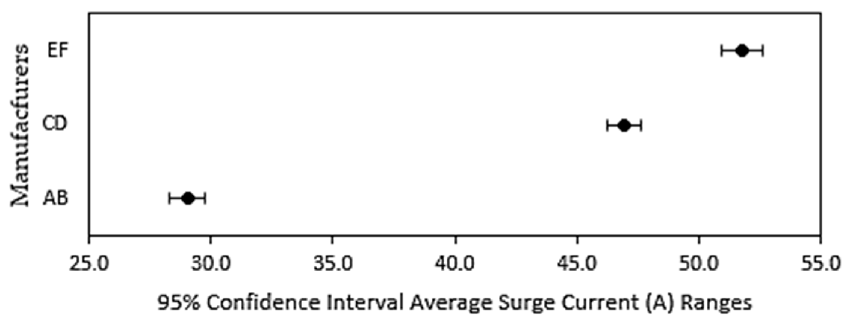
| AB | 29.0 A | 28.3 A | 29.8 A |
| CD | 46.9 A | 46.2 A | 47.6 A |
| EF | 50.9 A | 50.9 A | 52.6 A |
| Manufacturer | Lower Limit | Upper Limit | |
|---|---|---|---|
| AB | 202 W | 197 W | 207 W |
| CD | 321 W | 316 W | 326 W |
| EF | 357 W | 351 W | 362 W |
Disclaimer/Publisher’s Note: The statements, opinions and data contained in all publications are solely those of the individual author(s) and contributor(s) and not of MDPI and/or the editor(s). MDPI and/or the editor(s) disclaim responsibility for any injury to people or property resulting from any ideas, methods, instructions or products referred to in the content. |
© 2025 by the authors. Licensee MDPI, Basel, Switzerland. This article is an open access article distributed under the terms and conditions of the Creative Commons Attribution (CC BY) license (https://creativecommons.org/licenses/by/4.0/).
Share and Cite
van Niekerk, D.; Venter, J. Reliability Analysis of Transient Voltage Suppression Diodes Under Direct Current Switching Surge Stress. Energies 2025, 18, 1725. https://doi.org/10.3390/en18071725
van Niekerk D, Venter J. Reliability Analysis of Transient Voltage Suppression Diodes Under Direct Current Switching Surge Stress. Energies. 2025; 18(7):1725. https://doi.org/10.3390/en18071725
Chicago/Turabian Stylevan Niekerk, Daniel, and Johan Venter. 2025. "Reliability Analysis of Transient Voltage Suppression Diodes Under Direct Current Switching Surge Stress" Energies 18, no. 7: 1725. https://doi.org/10.3390/en18071725
APA Stylevan Niekerk, D., & Venter, J. (2025). Reliability Analysis of Transient Voltage Suppression Diodes Under Direct Current Switching Surge Stress. Energies, 18(7), 1725. https://doi.org/10.3390/en18071725