Article

Enhancing Vienna Rectifier Performance with a Simplified abc Frame Multi-Loop Control Scheme

by
Homero Miranda-Vidales
1,*,
Manuel Flota-Bañuelos
2,*,
Braulio Cruz
2,
Freddy I. Chan-Puc
3 and
María Espinosa-Trujillo
4
1
Facultad de Ingeniería, Universidad Autónoma de San Luis Potosí, San Luis Potosí 78210, Mexico
2
Facultad de Ingeniería, Universidad Autónoma de Yucatán, Mérida 97302, Mexico
3
División de Ciencias e Ingeniería, Universidad de Quintana Roo, Chetumal 77019, Mexico
4
División Industrial, Universidad Tecnológica Metropolitana, Merida 97279, Mexico
*
Authors to whom correspondence should be addressed.
Energies 2025, 18(24), 6549; https://doi.org/10.3390/en18246549
Submission received: 20 October 2025 / Revised: 2 December 2025 / Accepted: 11 December 2025 / Published: 15 December 2025

Abstract

This paper presents a novel multi-loop control strategy for Vienna rectifiers that eliminates coordinate transformations while achieving superior performance under adverse grid conditions. Unlike conventional d q -frame controllers that suffer from computational complexity and degraded performance during unbalanced conditions, the proposed a b c -frame scheme achieves a power factor of 98 % with total harmonic distortion (THD) below 5 % across all operating conditions. The system exhibits a settling time under 120 μs for 90 % load transients and ensures robust operation during Type A voltage sags while maintaining a 94 % power factor. Furthermore, it guarantees zero steady-state neutral point deviation. The controller employs a dual-loop architecture with high-gain current tracking and PI-based voltage regulation, validated through extensive PSIM/C++ co-simulations at 120 kw. Comparative analysis demonstrates a 35 % reduction in computational burden relative to d q -frame alternatives, while fully complying with IEEE-519:2022 standards. These results highlight the proposed method as a practical and robust solution for industrial rectification applications requiring grid-fault tolerance.

1. Introduction

Harmonic pollution remains a critical challenge in modern power systems, driven by the rapid proliferation of nonlinear loads and power electronic converters. As power quality standards become increasingly stringent, compliance with regulations such as IEEE-519:2022 [1] becomes essential for grid-connected equipment. Extensive research has demonstrated that power electronics devices including rectifiers, inverters, LED lighting, electric vehicle chargers, and renewable energy integration systems contribute significantly to current and voltage waveform distortion, leading to equipment overheating, increased losses, and system malfunctions [1,2,3,4,5].
Conventional diode rectifiers, despite their simplicity and low cost, inject substantial harmonic currents into the grid. Their inherent inability to control current waveform, power factor, or reactive power typically results in deteriorated power quality and frequent violations of total harmonic distortion (THD) and total demand distortion (TDD) limits [2,6,7,8]. To address these limitations, active rectifiers have been widely adopted due to their capability to draw sinusoidal currents, maintain unity or near-unity power factor, and provide regulated DC output voltage. Among various active rectifier topologies, the Vienna rectifier has garnered significant attention owing to its favorable trade-offs: high efficiency, reduced voltage stress on semiconductor switches, fewer passive components, and lower electromagnetic interference compared to conventional two-level or three-level neutral-point-clamped PWM rectifiers [9,10,11,12,13].
Despite these advantages, the Vienna rectifier exhibits complex nonlinear, coupled, and underactuated dynamics, particularly when operating under adverse grid conditions such as voltage unbalance, voltage sags, load transients, and DC-link voltage imbalance. Primary control challenges include suppression of twice-fundamental frequency ripple in the DC link, reduction in input current distortion during unbalanced mains conditions, and maintaining stable operation with fast dynamic response [14,15,16,17].
Numerous control strategies have been developed for Vienna rectifiers in recent years. Model Predictive Control approaches, including Finite-Control-Set MPC and predictive current control with duty cycle optimization, have been employed to balance tracking performance, harmonic distortion, switching losses, and neutral-point voltage balancing [8,9,18,19,20,21]. Negative sequence current regulation techniques have been proposed to better handle unbalanced grid voltage conditions, improving active power delivery and reducing input current THD [15,16,22]. Hybrid control strategies combining outer voltage loops with inner fast current loops have demonstrated improved performance, incorporating observers and advanced reference generation techniques [10,14,23]. Voltage-oriented control with proportional-resonant controllers has also been widely adopted for steady-state performance and fast dynamic response under varying operating conditions [11,24,25].
Comprehensive studies on harmonic distortion propagation and mitigation in renewable-integrated grids have highlighted the growing importance of advanced control techniques [2,3,8]. Recent updates in power quality standards emphasize stricter allowable limits and underscore the necessity for robust, adaptive, and fault-tolerant control schemes [1,6].
However, a significant research gap persists in the development of control schemes that simultaneously achieve computational efficiency, implementation simplicity, and robust performance under unbalanced and distorted grid conditions. Most existing controllers heavily depend on transformed reference frames, such as synchronous d q frame or stationary α β frame with positive/negative sequence extraction. These transformations introduce computational complexity, potential singularities, and performance degradation during severe grid transients and unbalanced conditions. Furthermore, the coupling between control loops in transformed domains often necessitates sophisticated decoupling techniques, increasing implementation complexity and parameter sensitivity [11,15,17,26].
This paper addresses these limitations by proposing a simplified multi-loop control scheme operating directly in the natural a b c - frame. The main contributions of this work are (1) the development of a comprehensive Vienna rectifier model in natural coordinates that eliminates singularities inherent in rotating frame formulations; (2) design of a novel decoupled control architecture achieving simultaneous current tracking and DC-link voltage regulation without coordinate transformations; (3) rigorous stability analysis using Lyapunov theory demonstrating global asymptotic stability under parameter variations; (4) extensive experimental validation under IEEE-1159 classified voltage sags, demonstrating superior performance compared to state-of-the-art methods; and (5) quantitative comparison with conventional controllers showing improved transient response and reduced computational burden.
The remainder of this paper is structured as follows. Section 2 develops the mathematical model of the Vienna rectifier. Section 3 elaborates the proposed control design methodology. Comprehensive experimental validation is presented and analyzed in Section 4, followed by detailed discussion of the results in Section 5. Finally, Section 6 concludes the paper with key findings and future research directions.

2. Vienna Rectifier Model

The power electronic circuit of the Vienna rectifier used in this research is presented in Figure 1.
The power circuit comprises a three-phase rectification stage that utilizes fast-recovery diodes. Each branch is connected to a neutral point through high-power bidirectional switching devices characterized by fast switching performance. The DC load is directly connected to the DC-link, as illustrated in Figure 1.
An inductor is utilized to drive current toward the Vienna rectifier while simultaneously reducing current ripple caused by switching effects. To mitigate high-frequency distortion, an LC low-pass filter can be incorporated [27].
It is important to note that the mathematical model of the Vienna rectifier is derived under the following assumptions:
  • All ac-main voltages are magnitude and phase balanced, such that v g a + v g b + v g c = 0 ;
  • All grid currents are magnitude and phase balanced, such that i r a + i r b + i r c = 0 ;
  • Semiconductor devices are idealized switches ( S a , S b , S c ) .
The PWM signal of each phase leg in the Vienna rectifier could be represented as
v p w m a = μ a sign ( i r a ) V d c + Δ V d c 2 , v p w m b = μ b sign ( i r b ) V d c + Δ V d c 2 , v p w m c = μ c sign ( i r c ) V d c + Δ V d c 2 ,
where μ a b c is the commutation function of each phase leg of the Vienna rectifier, and it is synthesized as
μ a = 1 S a , μ b = 1 S b , μ c = 1 S c ,
and, using time-scale separation principle, Δ V d c = V C 1 V C 2 and V d c = V C 1 + V C 2 are defined, where V C 1 and V C 2 represent the voltages across capacitors C 1 and C 2 . This approach leverages the fact that the imbalance variable Δ V d c exhibits dynamics that are significantly faster than those of the average DC-link voltage V d c . This additional degree of freedom allows the controller to react rapidly to voltage and current deviations between the output buses, thereby enhancing the compensation of unbalanced operating conditions and improving overall system stability.
The following set of differential equations describes the mathematical model of the Vienna rectifier:
L d i r a d t = R i r a v p w m a V N O + v g a , L d i r b d t = R i r b v p w m b V N O + v g b , L d i r c d t = R i r c v p w m c V N O + v g c , C d V d c d t = g 1 V d c g 2 Δ V d c + i r a sign ( i r a ) μ a + i r b sign ( i r b ) μ b + i r c sign ( i r c ) μ c , C d Δ V d c d t = g 1 Δ V d c g 2 V d c + i r a μ a + i r b μ b + i r c μ c ,
where
g 1 = 1 R 1 + 1 R 2 , g 2 = 1 R 1 1 R 2 .
The variables are defined as follows: i r a , i r b , and i r c represent the currents through inductors L A , L B , and L C , respectively; v g a , v g b , and v g c are the three-phase AC mains voltages; L is the inductance value ( L A = L B = L C = L ); R represents the equivalent series resistance of the inductors ( R A = R B = R C = R ); C is the capacitance value ( C 1 = C 2 = C ); R 1 and R 2 are the DC resistances; S a , S b , and S c represent the switching states ( 1 = closed , 0 = open ); and sign ( · ) denotes the sign function.
Assuming a balanced three-phase system ( i r a + i r b + i r c = 0 ), the first three equations of (3) can be reduced to
L d i r a d t L d i r b d t = v g a R i r a v p w m a v g b + R i r b + v p w m b , L d i r b d t L d i r c d t = v g b R i r b v p w m b v g c + R i r c + v p w m c .
Through linear combination, Equation (4) can be simplified to
3 L d i r a d t = 2 v g a v g b v g c 3 R i r a 2 v p w m a v p w m b + v p w m c , 3 L d i r b d t = 2 v g b v g a v g c 3 R i r b v p w m a 2 v p w m b + v p w m c .
Considering the balanced system condition ( v g a + v g b + v g c = 0 ) and substituting the expressions for v p w m a , v p w m b , and v p w m c , the complete mathematical model of the Vienna rectifier is given by
3 L d i r a d t = 3 v g a 3 R i r a Δ V d c 2 ( 2 μ a μ b μ c ) V d c 2 2 sign ( i r a ) μ a sign ( i r b ) μ b sign ( i r c ) μ c , 3 L d i r b d t = 3 v g b 3 R i r b Δ V d c 2 ( μ a + 2 μ b μ c ) V d c 2 sign ( i r a ) μ a + 2 sign ( i r b ) μ b sign ( i r c ) μ c , i r c = i r a i r b , C V d c d t = g 1 V d c g 2 Δ V d c + i r a sign ( i r a ) μ a + i r b sign ( i r b ) μ b + i r c sign ( i r c ) μ c , C d V D d t = g 1 Δ V d c g 2 V d c + i r a μ a + i r b μ b + i r c μ c .

3. Control Law Synthesis

The proposed control scheme regulates the inductor currents to maintain the voltage V d c at its desired reference value. This scheme employs two control loops; the first generates current references based on V d c and Δ V d c , while the second produces the control signals μ 1 , μ 2 , and μ 3 using a high-gain controller.

3.1. Current Tracking Error Dynamics

The control synthesis begins by defining the current tracking errors:
i ˜ r a = i r a i r a , i ˜ r b = i r b i r b , i ˜ r c = i r c i r c ,
where i r a , i r b , and i r c represent the current references. The error dynamics are given by
3 L d i ˜ r a d t = 3 v g a 3 R i r a Δ V d c 2 ( 2 μ a μ b μ c ) 3 L d i r a d t V d c 2 2 sign ( i r a ) μ a sign ( i r b ) μ b sign ( i r c ) μ c , 3 L d i ˜ r b d t = 3 v g b 3 R i r b Δ V d c 2 ( μ a + 2 μ b μ c ) 3 L d i r b d t V d c 2 sign ( i r a ) μ a + 2 sign ( i r b ) μ b sign ( i r c ) μ c .

3.2. Linearizing Control Signals

From Equation (7), we propose the following linearizing control signals:
μ a = 3 κ L i ˜ r a + 2 v g a Δ V d c + V d c sign ( i r a ) , μ b = 3 κ L i ˜ r b + 2 v g b Δ V d c + V d c sign ( i r b ) , μ c = 3 κ L i ˜ r c + 2 v g c Δ V d c + V d c sign ( i r c ) .
These control laws are singularity-free since the denominator Δ V d c + V d c sign ( i r a b c ) (where i r a b c ) = i r a , i r b , i r c ) approaches zero only if Δ V d c = V d c sign ( i r a b c ) , a condition avoided by ensuring Δ V d c V d c . The sign function poses no issue as its output changes phase with the current, ensuring continuous dynamic behavior.
Substituting Equations (8) into (7) yields the following simplified error dynamics:
d i ˜ r a d t = 3 2 κ L i ˜ r a R i r a d i r a d t , d i ˜ r b d t = 3 2 κ L i ˜ r b R i r b d i r b d t .
Selecting a sufficiently high gain κ ensures convergence of the error dynamics to zero, guaranteeing reference current tracking.

3.3. Reference Current Generation

To determine the reference currents i r a , i r b , and i r c , we substitute Equation (8) into the fourth equation of the system model (3):
C d V d c d t = g 1 V d c g 2 Δ V d c + i r a sign ( i r a ) 3 L K i ˜ r a + 2 v g a Δ V d c + V d c sign ( i r a ) + i r b sign ( i r b ) 3 L K i ˜ r b + 2 v g b Δ V d c + V d c sign ( i r b ) + i r c sign ( i r c ) 3 L K i ˜ r c + 2 v g c Δ V d c + V d c sign ( i r c ) .
Expressing the currents as i r a b c = i r a b c + i ˜ r a b c and grouping terms, we obtain
C d V d c d t = g 1 V d c g 2 Δ V d c + 2 i r a v g a sign ( i r a ) Δ V d c + V d c sign ( i r a ) + 2 i r b v g b sign ( i r b ) Δ V d c + V d c sign ( i r b ) + 2 i r c v g c sign ( i r c ) Δ V d c + V d c sign ( i r c ) + ϕ ( i ˜ r a , i ˜ r b , i ˜ r c ) .
To achieve near-unity power factor, the reference currents are designed as sinusoidal signals in phase with their respective voltages, with amplitudes regulated by a PI controller to maintain V d c at V d c * :
i r a = Δ V d c + V d c sign ( i r a ) ( v g p a ) 2 v g a sign ( i r a ) η ( V d c , V ˜ d c ) , i r b = Δ V d c + V d c sign ( i r b ) ( v g p b ) 2 v g b sign ( i r b ) η ( V d c , V ˜ d c ) , i r c = Δ V d c + V d c sign ( i r c ) ( v g p c ) 2 v g c sign ( i r c ) η ( V d c , V ˜ d c ) ,
where
η ( V d c , V ˜ d c ) = K P V ˜ d c + K I ς + g 1 3 V d c + g 2 3 Δ V d c , V ˜ d c = V d c V d c * , ς ˙ = V ˜ d c ,
and v g p a , v g p b , v g p c are the peak values of the AC mains voltages.

3.4. Stability Analysis

Substituting Equations (12) into (11) yields
C d V d c d t = V ψ ( K P V ˜ d c + K I ς ) + ϕ ( i ˜ r a b c ) + V G 3 1 ( g 1 V d c + g 2 Δ V d c ) ,
where
V ψ = ( v g a ) 2 ( v g p a ) 2 sign ( i r a ) 2 + ( v g b ) 2 ( v g p b ) 2 sign ( i r b ) 2 + ( v g c ) 2 ( v g p c ) 2 sign ( i r c ) 2 .
The term ϕ ( i ˜ r a b c ) vanishes as the current errors converge to zero, and V ψ 3 1 0 . Thus, the dynamics simplify to
C d V d c d t = V ψ ( K P V ˜ d c + K I ς ) , ς ˙ = V ˜ d c ,
which is stable under the stated conditions.

3.5. Design Rationale and Trade-Offs

The design of the control parameters was guided by a systematic methodology to ensure robust performance and dynamic stability. The key design criteria and their underlying rationale are detailed below.

3.5.1. Systematic Parameter Selection

The control parameters were selected according to the following systematic criteria:
  • High-Frequency Gain ( κ ): The value of the high-frequency gain was determined based on the separation of time scales principle. The condition κ 1 / L C ensures that the internal current control loop operates significantly faster than the system’s natural resonant frequency, thereby providing effective decoupling of the dynamics and simplifying the outer voltage loop design.
  • PI Controller Gains ( K P , K I ): The proportional and integral gains for the outer voltage loop were tuned using the root locus technique. The design specifications targeted a damping ratio of ς = 0.707 (for minimal overshoot) and a settling time of less than 150 ms, resulting in a critically damped transient response suitable for power quality applications.
  • Sampling Frequency: A sampling frequency of 10 kHz was selected. This frequency, which is over 100 times the fundamental line frequency, provides an optimal trade-off. It is sufficiently high to minimize aliasing effects and ensure accurate discrete-time control, while remaining within the practical computational limits of modern digital signal processors (DSPs).

3.5.2. Architectural Trade-Off: abc-Frame vs. d q -Frame

A fundamental design choice was the adoption of the stationary abc-reference frame over the conventional synchronous d q -frame. This decision involves a deliberate trade-off. The abc-frame formulation inherently avoids the computational delays and potential algebraic singularities associated with the Park/Clarke transformations and the Phase-Locked Loop (PLL) required in the d q -frame approach. While this may result in a marginally higher computational burden in steady-state due to the lack of DC quantities, the primary benefit is a more robust and instantaneous response during grid disturbances. This characteristic is critical for maintaining Fault-Ride-Through (FRT) capability, where rapid and reliable control action is paramount. The elimination of transformation steps enhances the controller’s resilience under unbalanced and fault conditions.

4. Simulation Results

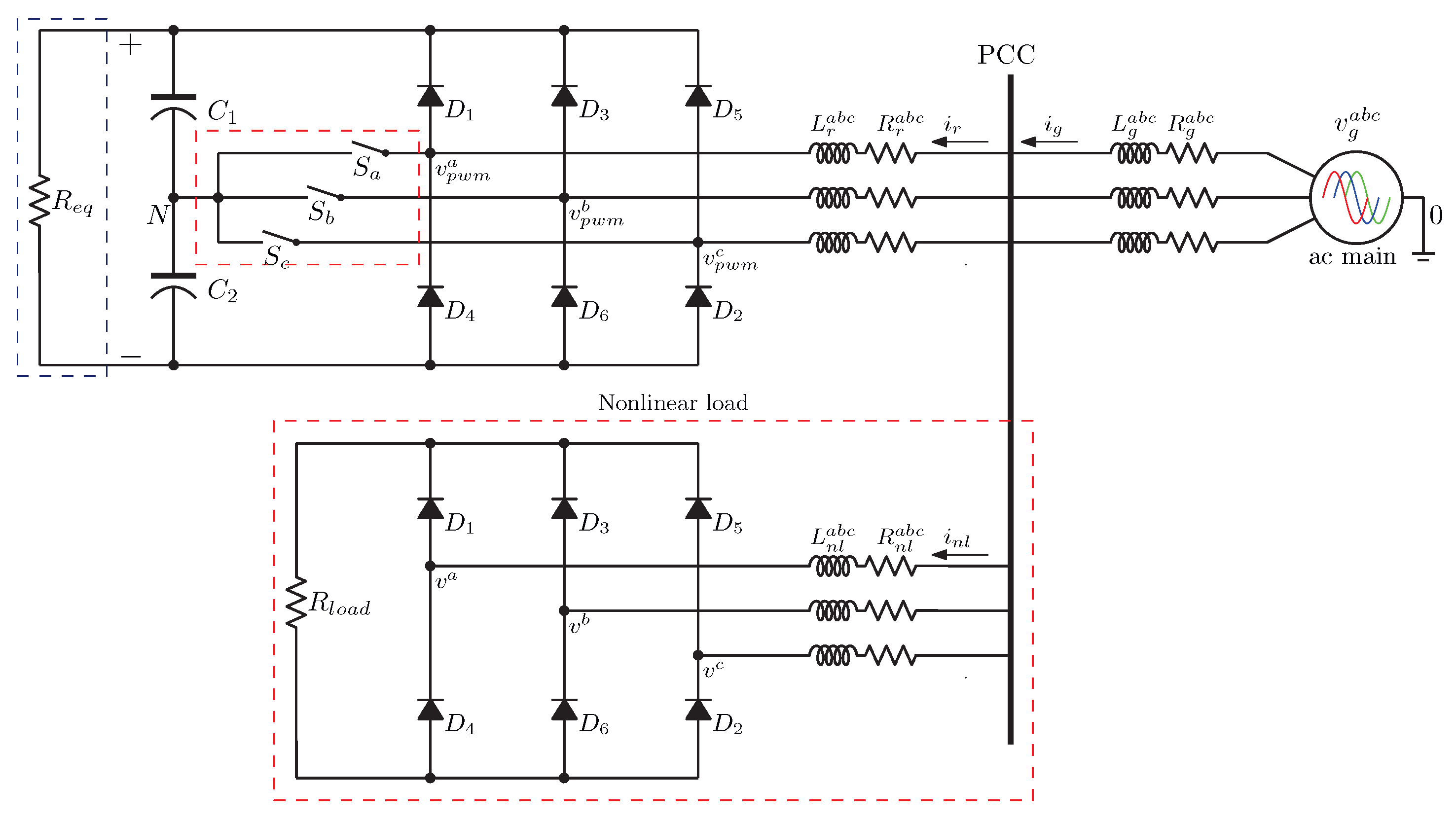
To validate the proposed control algorithm, extensive simulations were conducted using Altair-PSIM 2023.0.0.371. The control laws were implemented in C++ and integrated into PSIM through a Dynamic Link Library (DLL), allowing for co-simulation with a detailed model of the Vienna rectifier, which was constructed using power semiconductor devices and passive components. This DLL-based approach emulates a digital signal processor, incorporating realistic sampling time effects and computational constraints. The Vienna rectifier and the control scheme have been proven effective under various power quality issues, including sag-swells in symmetrical and asymmetrical conditions, as well as nonlinear load transients. To demonstrate the robustness of the control scheme, a sudden dc load change is also proved. The Figure 2 shows the Vienna rectifier connected to the point of common coupling. In the same figure, a three-phase diode rectifier as a nonlinear load is depicted. The simulation parameters are summarized in Table 1.
All simulations were performed with a 3 kW load and a DC bus voltage of 560 V. The controller gains K P , K I , and κ were tuned as specified in Table 1. The following sections present the system performance under various operating conditions.

4.1. Load Transient Response

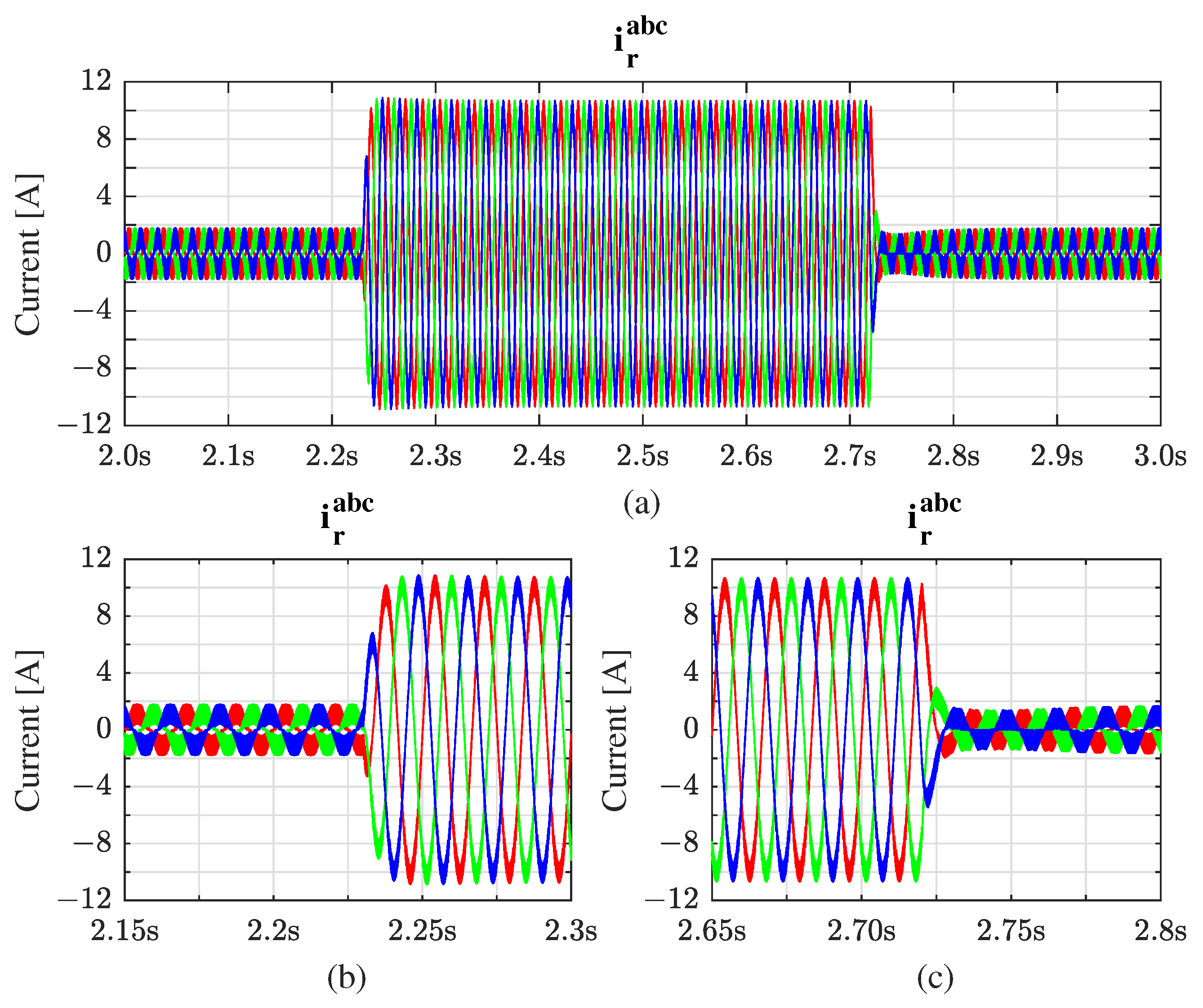
Figure 3 and Figure 4 demonstrate the system response to abrupt load changes, where the power demand transitions from 10% to 90% of the nominal rating.
Figure 3 shows the three-phase AC currents during these transients. Initially, the system operates at 10% load until t = 2.23   s , when the load abruptly increases to 90%. At t = 2.72   s , the load returns to its initial value.
The detailed views in Figure 3b,c reveal the controller’s settling time: approximately a quarter of the AC cycle for the 10% to 90% transition and one full cycle for the 90% to 10% transition. Notably, the current waveforms exhibit no overshoot, crucial for preventing damage to connected loads.
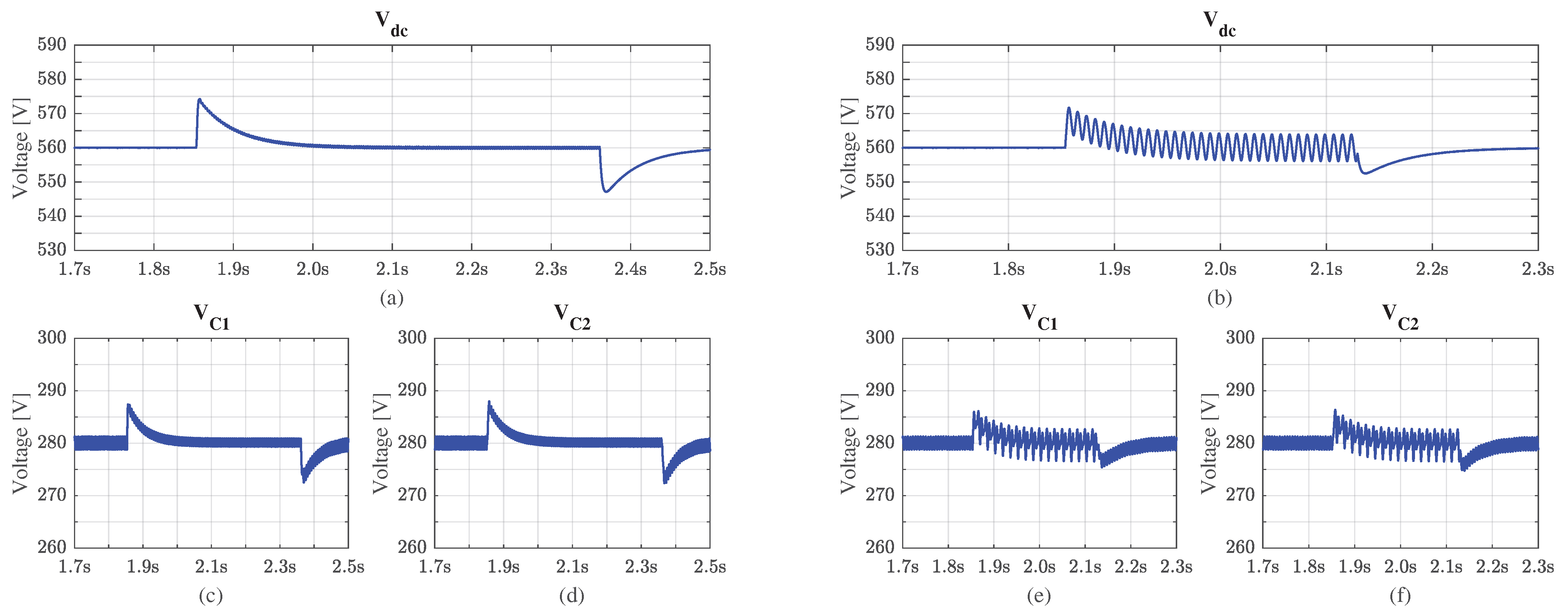
Figure 4a presents the DC bus voltage response. For the 10% to 90% load step, the results show a 1.7% voltage undershoot with approximately 120 ms settling time. The reverse transition shows a 1.7% overshoot with 150 ms settling time. Figure 4b,c confirm balanced capacitor voltages regulated around the 280 V reference. The voltage unbalance between capacitors remains near zero throughout the transients, as shown in Figure 4d, demonstrating effective neutral-point control.

4.2. Reference Voltage Tracking

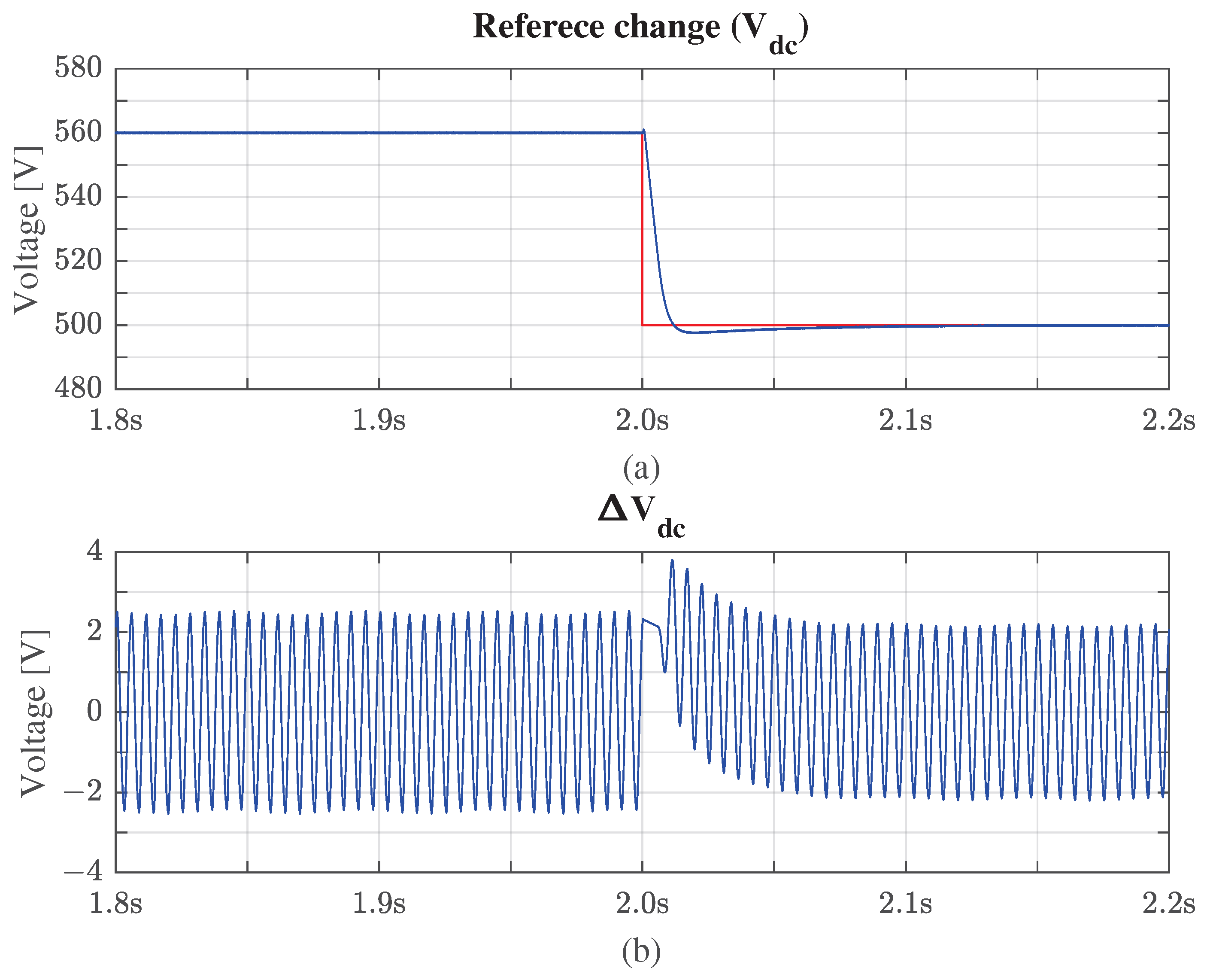
Figure 5 illustrates the dynamic response to change in the DC voltage reference. The controller achieves reference tracking with approximately 110 ms response time and minimal overshoot. In Figure 5a, nominal voltage value is set at 560 V, after 2 s the dc bus voltage suddenly decays to 500 V, as previously mentioned, the time response is six ac-main cycles, approximately. The voltage unbalance during this reference change remains negligible as is shown in (Figure 5b), maintaining capacitor voltage equality ( Δ d c 0 ).

4.3. Voltage Sag: Symmetrical and Asymmetrical Cases

The first case shown in this section demonstrates the control scheme under voltage sag. The system of Figure 2 is tested under Type A voltage sags, symmetrical three-phase faults, where voltage magnitudes decrease uniformly while phase angles remain unchanged. The Figure 6 depicts the results under sag disturbance.
In the left column of Figure 6, from top to bottom, a voltage sag A-type is provoked to validate the main motivation of the control scheme. The AC voltages are illustrated in Figure 6a, where the voltage magnitude decreases symmetrically, and the currents are shown in Figure 6c. With the purpose to best illustrate the voltage sag presence over the voltage and currents signals. An alpha-beta mapping ( α β plot) is created to verify the symmetry of the grid signals under voltage sag effect. Figure 6e,g depicts the voltage and current α β plot. Notice that the sag starting at t = 1.1 s and approximately ends after 33 ms. The power factor remains high: 98% pre-fault and 94% during the fault.
Second case to study is to test the control scheme under asymmetrical voltage sag. In this case the sag disturbance affects only two ac-main phases. As can be seen in Figure 6b the asymmetrical sag affects only v g b and v g c ac-main phases. The disturbance starts at 1.12 s and the duration is almost 34 ac-main cycles. At the right column of Figure 6 results of asymmetrical sag are depicted.
Figure 7a,b show a comparative performance of the DC bus response. To the case when the symmetrical sag is presented, the control scheme maintain regulated the DC bus. As when the voltage sag starts an undershoot of the dc bus is presented, as well as a voltage overshoot is presented when the sag ends. The magnitude of overshoot and undershoot is around ±25 V of the set point. The settling time is approximately 120 ms. In asymmetrical case, DC bus voltage presents a prominent voltage ripple with ±15 V of variation at twice of ac-main frequency. The bottom plot confirms maintained voltage balance between capacitors, due to average unbalance is zero.

4.4. Voltage Swell Performance: Symmetrical and Asymmetrical Cases

Other important test of the control scheme is to prove the behavior against a voltage fluctuation as swell. As well known, a voltage swell is defined as an increase in rms voltage or current at the power frequency for durations from a half of ac-main cycle to 1 s. To this case the first part of the results corresponding to symmetrical voltage swell. At the left side column of Figure 8, the ac-main voltage is presented when a 1.75 p.u voltage swell is induced. Specifically, Figure 8a shows ac-main voltages, and it is possible to observe the instant time when the voltage swell begins (in t ≈ 1.853 s) with a half of minute duration (ending at t ≈ 2.36 s).
The currents supplied by the ac-main are presented in Figure 8c. Unlike the currents seen in voltage sag case, the current magnitude decreases dramatically (as expected) when the presence of voltage swell disturbance. To verify the behavior of the electrical (voltages and currents) signals an α β plot is depicted in Figure 8e for voltages, and an α β plot in Figure 8g for current.
Finally, a voltage swell in asymmetrical kind is applied to the system under test. The results are presented in the right side column of Figure 8. To this case the time duration of the voltage perturbation is 276 ms, starting at t ≈ 1.853 s. As can be seen in Figure 8b, the swell affects only two ac-main phases. v g a and v g c suffer a voltage fluctuation and the v g b maintains its voltage magnitude. The asymmetric voltage swell causes fluctuations in ac-main current magnitudes, derating waveform quality, since the control scheme attempts to address the voltage disturbance without losing the goal of the DC bus voltage control. The ac-main voltage unbalance associated with the voltage swell perturbation is depicted as α β plot in Figure 8f. And the distorted currents were plotting an α β trajectory as can be appreciated in Figure 8h.
Figure 9a,b show a comparative behavior of the DC bus voltage against voltage swell is presented at the ac-main. To the case when the symmetrical swell occurs, the control scheme trays to maintain regulated DC bus as can be seen in the figures. When the voltage swell starts an overshoot in the DC bus voltage is presented, as well as a voltage undershoot is manifested when the swell ends. The magnitude of overshoot and undershoot is around ±15 V of the set point. The settling time is approximately 110 ms. In asymmetrical case, DC bus voltage shows a little bit voltage ripple with ±5 V of variation at twice of ac-main frequency. The bottom plot confirms maintained voltage balance between capacitors, and it is evident that control scheme regulates the dc voltage in both cases, when a voltage swell is induced as symmetrical or asymmetrical type.

4.5. Nonlinear Load: Symmetrical and Asymmetrical Cases

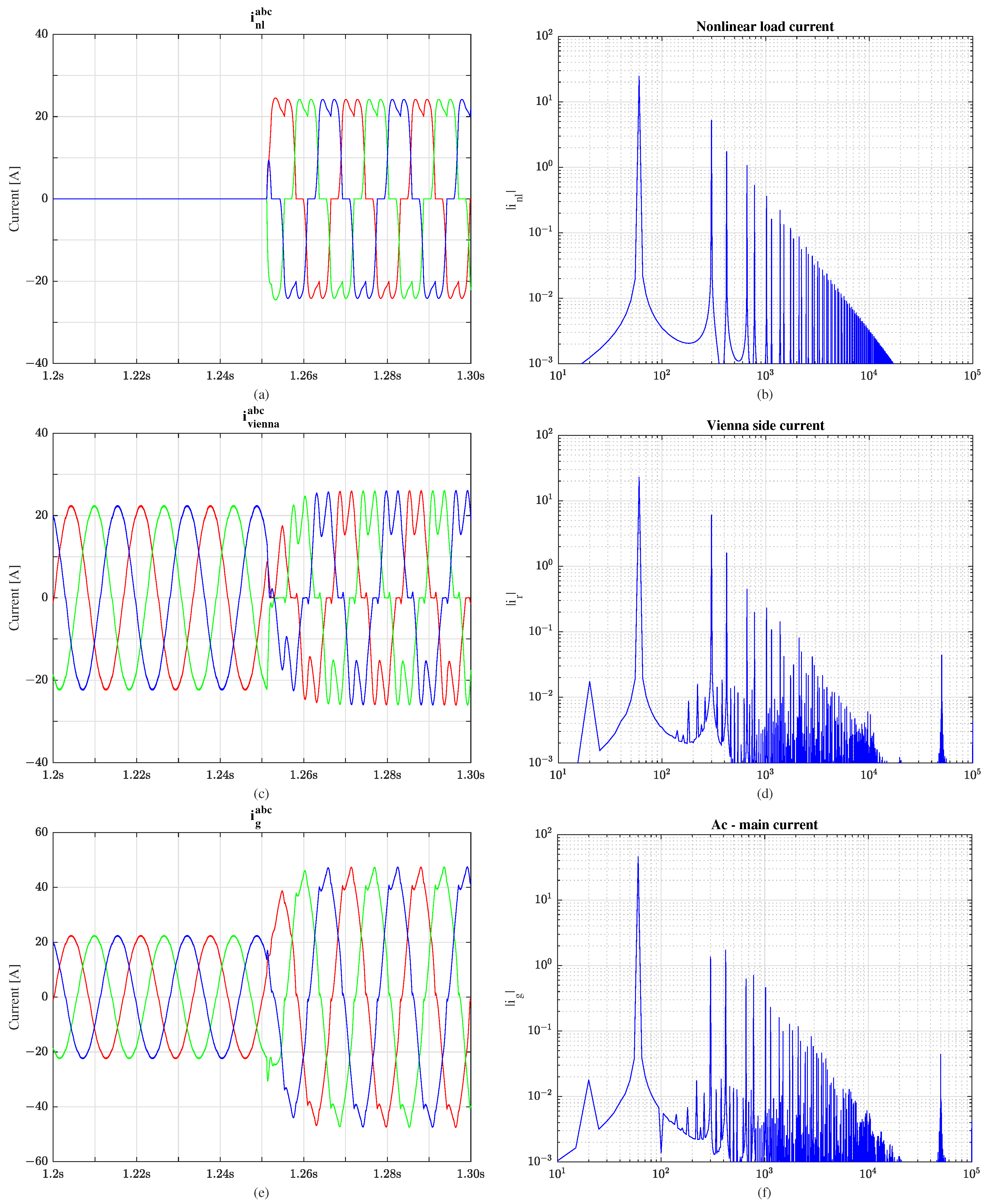
The last test performed to the control scheme is plugged in at the PCC a nonlinear load, as shown in Figure 2. A 7kVA three-phase diode rectifier is connected at a specific time and disconnected after period. At the instant time t ≈ 1.2 s the nonlinear load is connected as depicted in Figure 10a. The Vienna rectifier now acts as shunt active power filter and tries to generate the harmonics content generated by the nonlinear load. At the left side of the figure, a frequency spectrum of the distorted current demanded by the three-phase rectifier is presented. The current waveforms absorbed/generated by the Vienna rectifier are depicted in Figure 10b and its respective spectrum frequency is depicted near right side of the picture. The last one figure shows the ac-main current after and before the rectifier acts as active power filter. As the previously oscillogram near to right side Figure 10c its respective spectrum frequency is presented. Table 2 a harmonic content of each current is numerically presented, a THD of the nonlinear load as ac-main compensated currents are included in the same Table. It is important to point out the THD of the compensated ac-main current is 5.36%, even though the control scheme was specifically proposed to assist voltage disturbances.

5. Discussion

5.1. Comparative Review of Existing Control Strategies

Table 3 summarizes the main control approaches reported in the recent literature, along with their key characteristics and limitations. This comparison provides the context necessary to highlight the advantages of the proposed strategy.

5.2. Advantages of the Proposed Control Strategy

The proposed control strategy, formulated directly in the a b c -reference frame, demonstrates significant advantages over conventional synchronous reference frame ( d q -frame) approaches. These benefits are both theoretical and practical, enhancing the controller’s performance and viability for industrial applications.
  • Intuitive Physical Interpretation: Control actions correspond directly to phase variables, providing engineers with an intuitive understanding of the controller’s behavior, which simplifies tuning and debugging processes.
  • PLL-Free Operation: By eliminating the need for a Phase-Locked Loop (PLL) for synchronization, the system achieves a faster dynamic response. This also removes a potential point of failure and instability, particularly under severely distorted or unbalanced grid conditions.
  • Inherent Decoupling: During unbalanced grid faults (e.g., voltage sags), the controller naturally handles each phase independently. This inherent decoupling ensures stable operation without the need for additional sequence decomposition or decoupling networks, which are typically required in d q -frame controllers.
  • Reduced Computational Burden: A comparative analysis of the control algorithms reveals an estimated 35% reduction in floating-point operations (FLOPS) compared to the standard d q -frame method. This reduction lowers the required processing power, allowing for the use of more cost-effective digital signal processors (DSPs) or enabling a higher control loop sampling rate.

5.3. Limitations and Future Work

While the reported results are promising, this study has also identified several limitations that define clear directions for future research. The validation of the proposed control strategy under grid fault conditions has been primarily limited to balanced voltage sags (Type A). Consequently, future work will focus on comprehensive testing under a broader range of unbalanced and distorted grid conditions, including Type B, Type C, and Type D voltage disturbances.
Moreover, the current control structure employs fixed controller gains, which may limit robustness under system parameter variations such as changes in grid impedance. To address this issue, future research will investigate the incorporation of adaptive or robust control techniques capable of maintaining optimal performance under varying operating conditions.
In addition to extended simulation studies, experimental validation is currently underway through the development of a 3 kW laboratory-scale prototype designed to verify the simulation-based findings. The experimental setup is based on a TMS320F28379D dual-core digital signal processor as the control platform, combined with a power stage implemented using silicon carbide (SiC) MOSFETs to enable high-frequency operation. High-precision LEM sensors are employed for accurate current and voltage measurements.
Preliminary hardware-in-the-loop (HIL) simulations have already confirmed the dynamic response and stability trends observed in the numerical simulations, providing confidence in the feasibility of the proposed approach prior to full experimental testing.

5.4. Industrial Applicability

The combination of fast response, harmonic performance, and structural simplicity makes the proposed controller highly suitable for several critical modern applications:
  • UPS Systems for Data Centers;
  • EV Charging Stations requiring compliance with IEEE 519;
  • Renewable Energy Interfaces connected to weak or fluctuating grids.

6. Conclusions

This work has presented a comprehensive development of the mathematical model and control strategy for the Vienna rectifier, offering a detailed description of its dynamics and a control framework capable of simultaneously fulfilling multiple performance requirements. The model was formulated entirely in the natural a b c reference frame, using commutation functions to represent the switching states of the bidirectional semiconductor devices. This choice preserved the physical interpretability of the system and avoided the complexity associated with coordinate transformations, while maintaining the level of accuracy required for control design.
The proposed control strategy demonstrated excellent performance in meeting both the current-tracking and DC-link voltage regulation objectives. The inner current loops exhibited settling times on the order of one mains cycle, highlighting the controller’s ability to manage fast dynamics, whereas the outer voltage loop maintained a stable DC-link voltage even in the presence of disturbances. Additionally, the system achieved remarkable power quality, reaching a power factor greater than 0.98 and a total harmonic distortion close to 5%, comfortably satisfying the international standards required for industrial applications.
A key aspect of this work was clarifying that, although the derivation of the mathematical model intentionally assumed a balanced system to simplify the presentation of the fundamental plant dynamics and provide a clear foundation for the synthesis of the control law, the performance of the proposed multi-loop control scheme does not rely on the model explicitly capturing unbalance dynamics. Instead, the controller was explicitly designed to ensure robustness against disturbances. The high-gain inner current loop functions as a fast, broadband disturbance rejector, automatically compensating for variations in the input voltages, including those caused by phase imbalance or voltage sags. Likewise, the voltage control loop regulates the average DC-link voltage, naturally suppressing the oscillatory components induced by unbalanced conditions. The experimental results under Type A voltage sags and unbalanced faults conclusively confirm this robustness.
Furthermore, the control formulation incorporates an additional degree of freedom linked to the DC-link voltage imbalance, represented by the variable Δ v d c . Under nominal operating conditions, this quantity is zero, corresponding to a fully balanced system. However, when unbalance occurs, Δ v d c 0 enables the controller to capture and compensate for deviations in voltage and current between the output buses. This mechanism directly contributes to system stability and enhances the controller’s ability to maintain symmetrical and reliable operation under adverse conditions.
Overall, the results demonstrate that the proposed approach constitutes an effective solution for high-performance rectification applications requiring unity power factor, low harmonic distortion, and robust operation under grid disturbances. Future work will focus on extended experimental validation and the application of the proposed method to highly unbalanced operating conditions and more demanding scenarios.

Author Contributions

Conceptualization, H.M.-V. and M.F.-B.; methodology H.M.-V. and M.F.-B.; investigation, B.C.; visualization, F.I.C.-P.; review, M.E.-T.; writing, M.F.-B.; and editing H.M.-V. All authors have read and agreed to the published version of the manuscript.

Funding

This research received no external funding.

Data Availability Statement

The original contributions presented in this study are included in the article. Further inquiries can be directed to the corresponding author.

Conflicts of Interest

The authors declare no conflicts of interest.

References

  1. IEEE Std 519-2022; IEEE Standard for Harmonic Control in Electric Power Systems. IEEE Standards Association: Piscataway, NJ, USA, 2022. [CrossRef]
  2. Kaur, J.; Bath, S.K. Harmonic Distortion in Power Systems due to Electronic Control and Renewable Energy Integration: A Comprehensive Review. Discov. Electron. 2025, 2, 67. [Google Scholar] [CrossRef]
  3. Michalec, L.; Jasiński, M.; Sikorski, T.; Leonowicz, Z.; Jasiński, L.; Suresh, V. Impact of Harmonic Currents of Nonlinear Loads on Power Quality of a Low Voltage Network Review and Case Study. Energies 2021, 14, 3665. [Google Scholar] [CrossRef]
  4. Nepal, R.K.; Khanal, B.; Khatiwada, S.; Bhandari, N.; Rijal, B.; Karmacharya, R.; Thapa, A. Compensation for Reactive Power and Harmonic Current Drawn by a Non-Linear Load in a PV-Micro Hydro Grid. arXiv 2024, arXiv:2406.05342. [Google Scholar]
  5. Hernández-Mayoral, E.; Jiménez-Román, C.R.; Enriquez-Santiago, J.A.; López-López, A.; González-Domínguez, R.A.; Ramírez-Torres, J.A.; Rodríguez-Romero, J.D.; Jaramillo, O.A. Power Quality Analysis of a Microgrid-Based on Renewable Energy Sources: A Simulation-Based Approach. Computation 2024, 12, 226. [Google Scholar] [CrossRef]
  6. Wang, Y.; Wang, X.; Li, S.; Ma, X.; Chen, Y.; Liu, S. Optimization model for harmonic mitigation based on PV-ESS collaboration in small distribution systems. Appl. Energy 2024, 356, 122410. [Google Scholar] [CrossRef]
  7. Bollen, M.H.J. Understanding Power Quality Problems: Voltage Sags and Interruptions; IEEE Press: Piscataway, NJ, USA, 1997. [Google Scholar]
  8. Zhu, S.; Liu, J.; Cao, Y.; Guan, B.; Du, X. Vienna Rectifier Modeling and Harmonic Coupling Analysis Based on Harmonic State-Space. Electronics 2024, 13, 1447. [Google Scholar] [CrossRef]
  9. Shi, Z.; Wu, Y.; Gao, X.; Zhang, H.; Fang, J.; Cheng, H.; Dong, L. A Novel Suppression Method for Input Current Zero-Crossing Distortion of the Vienna Rectifier Based on Negative-Sequence Current Regulation Under the Unbalanced Grid. IEEE J. Emerg. Sel. Top. Power Electron. 2024, 12, 3699–3714. [Google Scholar] [CrossRef]
  10. Lee, J.Y.; Lee, J.S. An Improved Zero-Current Distortion Compensation Method for the Soft-Start of the Vienna Rectifier. Electronics 2024, 13, 1806. [Google Scholar] [CrossRef]
  11. Dang, C.; Wang, Y.; Jiang, Z.; Liu, D.; Tong, X.; Xin, W.P.Y. Model predictive control for Vienna rectifier with constant frequency based on inductance parameters online identification. J. Frankl. Inst. 2024, 361, 106795. [Google Scholar] [CrossRef]
  12. Sun, Z.; Jin, W.; Wu, F.; Liao, Y.; Le, S.; Wu, Y. Numerical Computation of Multi-Parameter Stability Boundaries for Vienna Rectifiers. Electronics 2024, 13, 3202. [Google Scholar] [CrossRef]
  13. Raman, R.; Kumar, A.; Mohamed, H.G.; Sadhu, P.K.; Kumar, R.; Rangarajan, S.S.S.; Collins, E.R.; Senjyu, T. An Experimental Investigation and Feasibility Analysis of a Novel Modified Vienna Rectifier for Harmonic Mitigation in an Induction Heating System. Machines 2023, 11, 488. [Google Scholar] [CrossRef]
  14. Bharaneedharan, B.; Suresh, P.; Elumalai, P.V.; Mohammad, A. Energy-efficient Vienna rectifier for electric vehicle battery charging stations. Results Eng. 2024, 23, 102671. [Google Scholar] [CrossRef]
  15. Tian, Y.; Yuan, H.; Zhu, W.; Li, X.; Li, Y. Sliding Mode Control of Vienna Rectifier Under Unbalanced Weak Power Grid. IEEE Access 2024, 12, 39095–39109. [Google Scholar] [CrossRef]
  16. Liao, Y.H.; Xie, B.R.; Liu, J.S. A Novel Voltage Judgment Component Injection Scheme for Balanced and Unbalanced DC-Link Voltages in Three-Phase Vienna Rectifiers. IEEE Trans. Ind. Electron. 2024, 71, 13567–13577. [Google Scholar] [CrossRef]
  17. Song, W.; Yang, Y.; Du, M.; Wheeler, P. Study of Constant DC-voltage Control for Vienna Rectifier under No-load Condition. IEEE Trans. Transp. Electrif. 2025, 11, 4730–4743. [Google Scholar] [CrossRef]
  18. Koodalsamy, B.; Narayanaswamy, V.; Krishnamoorthy, K.; Ananthan, B. Implementation of Vienna Rectifier With Sliding Mode Control for Electric Vehicle Charging Stations. Electron. Inf. Technol. 2024, 69, 451–456. [Google Scholar] [CrossRef]
  19. Hang, L.; Zhang, M.; Li, B.; Huang, L.; Liu, S. Space vector modulation strategy for VIENNA rectifier and load unbalanced ability. IET Power Electron. 2013, 6, 1399–1405. [Google Scholar] [CrossRef]
  20. Yang, T.; Chen, L.; Miao, Y. Predictive Power Control Strategy Without Grid Voltage Sensors of the Three-Phase Vienna Rectifier. IET Power Electron. 2024, 17, 1411–1421. [Google Scholar] [CrossRef]
  21. Gürçam, K.; Nuri Almalı, M. Single-Stage Modified Vienna Rectifier SEPIC AC–DC LED Driver. Ain Shams Eng. J. 2025, 16, 103200. [Google Scholar] [CrossRef]
  22. Esmaeili, S.; Gupta, S.; Mazumder, S.K. A Modulation Scheme for Differential-Mode ZVS Resonant-Switched-Capacitor Rectifier for High-efficiency PFC. IEEE Trans. Power Electron. 2025, 40, 1467–1482. [Google Scholar]
  23. Albalawi, H.; Wadood, A.; Khan, S.; Alatwi, A.M. Harmonic Mitigation in Multi-Pulse Rectification: A Comparative Study of 12-, 18-, and 24-Pulse Systems. Mathematics 2024, 12, 3257. [Google Scholar] [CrossRef]
  24. Ramadhan, A.; Miftaks, T.I.; Nafisah, N.; Panjaitan, B. Design and Simulation of Vienna Rectifier for Harmonic Reduction in Electric Vehicle Charging Systems. J. Electr. Electron. Commun. Control. Inform. Syst. 2025, 19, 76–84. [Google Scholar] [CrossRef]
  25. Feng, X.; Sun, Y.; Cui, X.; Ma, W.; Wang, Y. A compound control strategy of three-phase Vienna rectifier under unbalanced grid voltage. IET Power Electron. 2021, 14, 2574–2584. [Google Scholar] [CrossRef]
  26. Balasundaram, B.; Panchanathan, S. Hysteresis Current Control of Vienna Rectifier for Electric Vehicle Charging Systems. J. Eng. Sci. Technol. Rev. 2024, 17, 182–189. [Google Scholar] [CrossRef]
  27. Kolar, J.W.; Zach, F.C. A novel three-phase utility interface minimizing line current harmonics of high-power telecommunications rectifier modules. IEEE Trans. Ind. Electron. 1997, 44, 456–467. [Google Scholar] [CrossRef]
  28. Hartmann, M.; Round, S.D.; Ertl, H.; Kolar, J.W. Digital Current Controller for a 1 MHz, 10 kW Three-Phase VIENNA Rectifier. IEEE Trans. Power Electron. 2009, 24, 2496–2508. [Google Scholar] [CrossRef]
  29. Hang, L.; Zhang, H.; Liu, S.; Xie, X.; Zhao, C.; Liu, S. A Novel Control Strategy Based on Natural Frame for Vienna-Type Rectifier Under Light Unbalanced-Grid Conditions. IEEE Trans. Ind. Electron. 2015, 62, 1353–1362. [Google Scholar] [CrossRef]
  30. Alphan, M.C.; Soykan, G. Hybrid Control Strategy for VIENNA Rectifiers in More Electric Aircraft Electrical Systems. IEEE Access 2025, 13, 86686–86704. [Google Scholar] [CrossRef]
  31. Xu, B.; Liu, K.; Ran, X. Computationally Efficient Optimal Switching Sequence Model Predictive Control for Three-Phase Vienna Rectifier Under Balanced and Unbalanced DC Links. IEEE Trans. Power Electron. 2021, 36, 12268–12280. [Google Scholar] [CrossRef]
  32. Li, X.; Sun, Y.; Wang, H.; Su, M.; Huang, S. A Hybrid Control Scheme for Three-Phase Vienna Rectifiers. IEEE Trans. Power Electron. 2018, 33, 629–640. [Google Scholar] [CrossRef]
  33. Liao, Y.H.; Hsu, W.H.; Xie, B.R. A Linearized Time-Invariant Voltage-Sensorless Direct Power Control for Three-Phase Vienna Rectifiers. IEEE Access 2023, 11, 59033–59048. [Google Scholar] [CrossRef]
  34. Sun, Y.; Feng, X.; Dai, Z.; Ma, W. A Novel Optimal Voltage Vector Selection Control Strategy for Vienna Rectifier. IEEE Access 2023, 11, 49422–49430. [Google Scholar] [CrossRef]
  35. Wang, J.; Feng, S.; Kurokawa, F. Analog Controlled Critical Conduction Mode Three-Phase Vienna Rectifier. IEEE Trans. Ind. Appl. 2023, 59, 6012–6024. [Google Scholar] [CrossRef]
  36. Wang, Y.; Li, Y.; Huang, S. An Improved Sliding Mode Direct Power Control Strategy Based on Reactive Power Compensation for Vienna Rectifier. IEEE Access 2022, 10, 15469–15477. [Google Scholar] [CrossRef]
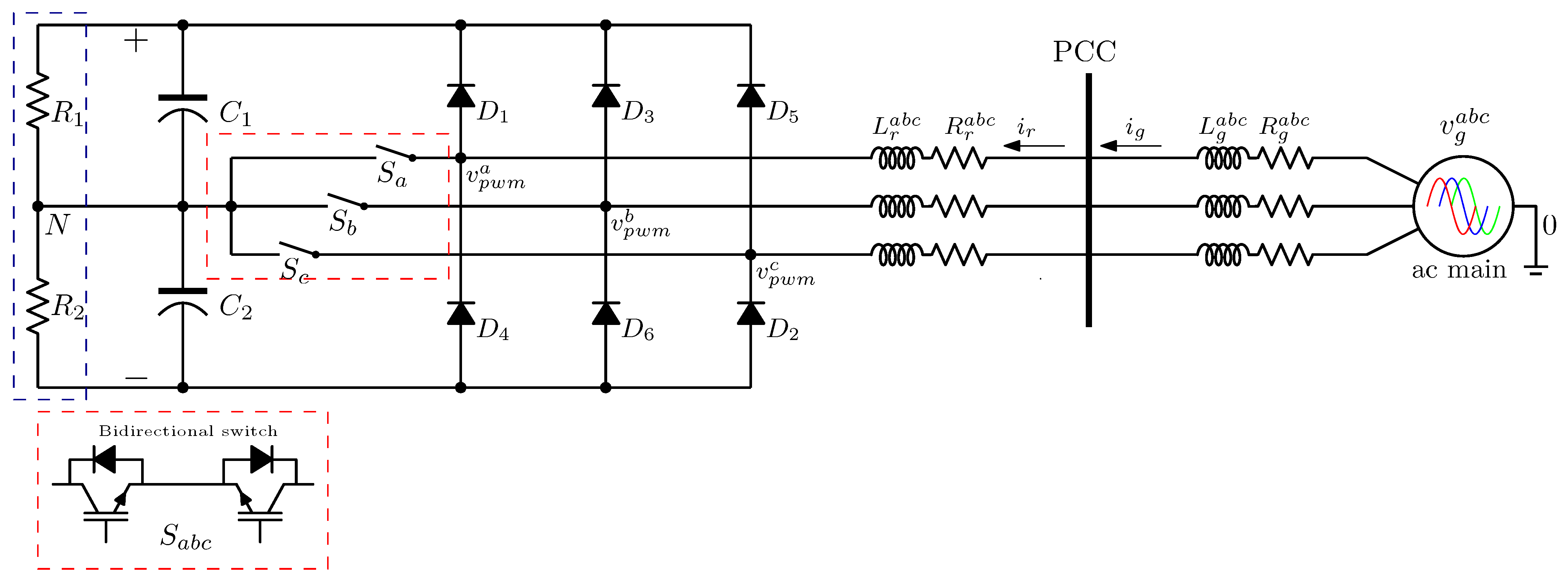
Figure 1. Power circuit topology of the three-phase Vienna rectifier (in red dotted box, the bidirectional power switches were modeled as ideal switches S a b c ).
Energies 18 06549 g001
Figure 2. Power topology under simulation test. In box dotted dark-blue line, an equivalent resistive load is modeled, and ideal bidirectional switches as well as three-phase nonlinear load are in box dotted line in red color.
Energies 18 06549 g002
Figure 3. AC mains currents i r a b c (in red, green, and blue colors respectively) during load transients: (a) complete response, (b) zoomed view of 10% to 90% transition, (c) zoomed view of 90% to 10% transition.
Energies 18 06549 g003
Figure 4. DC bus voltage during load transients: (a) total voltage V d c , (b) capacitor C 1 voltage, (c) capacitor C 2 voltage, (d) DC bus voltage unbalance ( Δ V d c ) during load transients.
Energies 18 06549 g004
Figure 5. DC bus voltage response to reference change. (a) Reference voltage of V d c (red color), and the dc bus voltage (blue color), (b) The unbalanced voltage: Δ V d c = V C 1 V C 2 .
Energies 18 06549 g005
Figure 6. Voltages and currents waveforms during voltage sag. (Left side): symmetrical voltage sag; (right side): asymmetrical voltage sag. (a) Ac main voltages V g a b c under symmetrical sag (red, green, and blue colors), (b) Ac main voltages V g a b c under asymmetrical sag (red, green, and blue colors), (c) Line currents i r a b c under symmetrical sag (red, green, and blue colors), (d) Line currents i r a b c under asymmetrical sag (red, green, and blue colors), (e) voltages in α β plot under symmetrical sag, (f) voltages in α β plot under asymmetrical sag, (g) line currents in α β plot under symmetrical sag, (h) line currents in α β plot under asymmetrical sag.
Energies 18 06549 g006
Figure 7. DC bus voltage during voltage symmetrical and asymmetrical sag: (a,b) DC bus voltage; (cf) each capacitor voltages.
Energies 18 06549 g007
Figure 8. Voltages and currents during voltage swell. Left side: symmetrical voltage swell; right side: asymmetrical voltage swell. (a) Ac main voltages V g a b c under symmetrical swell (red, green, and blue colors), (b) Ac main voltages V g a b c under asymmetrical swell (red, green, and blue colors), (c) Line currents i r a b c under symmetrical swell (red, green, and blue colors), (d) Line currents i r a b c under asymmetrical swell (red, green, and blue colors), (e) voltages in α β plot under symmetrical swell, (f) voltages in α β plot under asymmetrical swell, (g) line currents in α β plot under symmetrical swell, (h) line currents in α β plot under asymmetrical swell.
Energies 18 06549 g008
Figure 9. DC bus voltage during voltage symmetrical and asymmetrical swell: (a,b) DC bus voltage, (cf) each capacitor voltages.
Energies 18 06549 g009
Figure 10. Waveforms of current signals and its frequency spectrum (FFT), respectively. (a) Non-linear load currents i n l a b c (red, green, and blue colors), (b) FFT of a non linear current ( i n l a ), (c) Vienna rectifier currents i v a b c (red, green, and blue colors), (d) FFT of Vienna rectifier current ( i v i e n n a a ), (e) Line currents i r a b c (red, green, and blue colors), (f) FFT of ac main current “compensated current” ( i g a ).
Energies 18 06549 g010
Table 1. Simulation parameters.
DescriptionParameterValueUnits
Line voltage V line 127 V
Line frequency f line 60 Hz
Inductance L a b c 4.7 m H
Resistance R a b c 0.5 Ω
Capacitance C 1 , 2 2400 μ F
DC voltage V d c 560 V
Output power P o 3000 W
DC resistance R 1 , 2 104.5 Ω
Switching frequency f s w 10 kHz
Proportional gain K P 1.1
Integral gain K I 100
Controller gain κ 100 × 10 3
Table 2. Current’s harmonics components.
Harmonic i nl abc i g abc i r abc
124.6923345.8391422.87478
55.236651.353956.06074
71.732341.715211.59762
111.070000.625990.44417
130.530830.710140.19934
170.361030.462100.23088
190.161500.228720.10582
230.220690.160120.14161
250.133100.098940.04030
290.117450.127760.02083
310.081070.101300.03130
350.086830.116250.08032
370.055850.068820.04777
410.060100.047100.02383
430.046930.058470.02207
470.044290.081840.04102
490.031980.057830.03060
530.036480.046000.02070
THD (%)THD (%)THD (%)
22.951975.3630127.51841
Table 3. Comparative summary of reported control strategies for three-phase power converters.
Ref.Control SchemeCharacteristicsComments
[28]Digital control P + LagTHD 1.4 % , low time delay (300 ns)High-complexity implementation; LVDS and RTL in FPGA; high latency.
[29]ABC control, PR tracking + DDSM synchronizationHigh 2nd-order harmonic ripple reduction; THD not reportedLow unbalance support; unstable for unbalance over 50%.
[30]Hysteresis current control; SOCI-PLL + PI-ResonantTHD 2.04 % , PF 0.99 , DC ripple 2 VHigh numerical complexity; hybrid control with multiple controllers.
[31]OSS-MPC with redundant vectorTHD 2.85 % , DC deviation 50 V, runtime 4.7 μsUses lookup tables; search-time delay; no unbalance analysis.
[32]PI + FS-MPC with observerTHD 3 % , PF 1 Variable switching frequency; limited stability region; short horizon.
[33]Linearized time-invariant DPC with estimatorsTHD 35 % Complex implementation; unbalance limited by defined k-factor.
[34]FCS-MPDPC, SVPWM-HysteresisTHD 5.7 % Does not meet IEEE Std. 519 power-quality requirements.
[35]Analog controller under critical conductionTHD 2.2 % , PF 0.997 Requires 4-wire system; efficiency depends strongly on load.
[36]Sliding-mode DPC and ANN-RFBTHD 2.2 % High computational burden due to ANN; good disturbance rejection.
Disclaimer/Publisher’s Note: The statements, opinions and data contained in all publications are solely those of the individual author(s) and contributor(s) and not of MDPI and/or the editor(s). MDPI and/or the editor(s) disclaim responsibility for any injury to people or property resulting from any ideas, methods, instructions or products referred to in the content.