Article

Investigations on Output Impedance Measurement of Digitally Controlled Power Converters with Wide Bandwidth Signals †

1
Institute of Power Electronics, Friedrich-Alexander-University, 91054 Erlangen, Germany
2
Fraunhofer Institute for Integrated Systems and Device Technology IISB, 91058 Erlangen, Germany
*
Author to whom correspondence should be addressed.
This paper extends the research of our paper “Output Impedance Measurement of Digitally Controlled Power Converters in LVDC-Grids” previously published at the 2024 IEEE International Conference on DC Microgrids, Columbia, SC, USA, 5–8 August 2024.
Energies 2025, 18(23), 6121; https://doi.org/10.3390/en18236121 (registering DOI)
Submission received: 17 October 2025 / Revised: 11 November 2025 / Accepted: 20 November 2025 / Published: 22 November 2025
(This article belongs to the Section F1: Electrical Power System)

Abstract

Impedance-based stability criteria can be a powerful tool in systems analysis of microgrids. Especially in terms of low-voltage direct current grids, the amount of available power converters continuously increases. Since commercial components are typically black-boxes for system analysis, reliable and fast measurement is required to allow for accurate stability estimations. Here, wide bandwidth signals offer reduced measurement time at high accuracy. Since higher power converters are often digitally controlled, this paper investigates requirements for proper wide bandwidth impedance measurement under the boundary conditions the digital control enforces on time and value quantization.

1. Introduction

The need for reliable and efficient energy distribution drives the development of low-voltage direct current (LVDC) grids. [1,2,3]. LVDC microgrids can either be connected to AC grids, with a certain level of autonomy, or operate completely autonomously, relying only on renewable energy sources. Through integration of battery storage systems and electric vehicles this autonomy can be even further increased [4,5,6,7,8].
However, maintaining stability in all operating conditions is required for ensuring the reliability of LVDC microgrid operation. This challenge becomes increasingly more difficult as the stability analysis needs to encompass an increasing number of components and converter types [9,10,11,12], making model-based predictions near impossible without knowledge about the internal system parameters. The application of measurement-based stability criteria can eliminate this issue. A promising group of stability criteria are based on the grid side impedance of converters [13,14,15,16,17,18,19,20,21,22], based on and adapted from [23]. Since impedance can be directly measured for a black-box system, stability information can be gained without further information about the converter itself. The only prerequisite is a measurement system capable of accurate impedance measurement of power converters.
Since most higher power converters used for LVDC microgrids are digitally controlled, methods of impedance measurement need to be investigated for their effect on digital control. Due to the added benefits in fast measurement, this paper will be focused on broad band measurements using pseudo random binary sequences (PRBSs).
PRBS signals have been used for system identification in various power electronics applications. Often the PRBS is generated by the system itself and modulated onto an internal signal like the converters duty cycle [24,25,26,27,28,29], which can then be used to identify control loop transfer functions. Even using multiple orthogonal PRBSs simultaneously within a larger system have been investigated [30,31,32]. In AC systems these orthogonal signals can even be used to measure reactive and active current control loops as well as their interactions [33,34]. If the PRBS is used to excite a connected converter, or even the whole grid, impedance measurement of unknown converters is also possible [35,36,37]. PRBS signals have also been modified from being classical maximum length two state signals, to three state signals [34,38,39] or optimized two state signals [40], to enhance certain frequency component’s power density.
While being widely used, the typical recommendation for the signal amplitude is somewhere in the low single digit percentage range [28,33,37], high single digit percentage range [35,36], or up to 25% [27] of the steady state values depending on application. These amplitudes all have been determined by trial and error, not based on fundamental principles. In [28] the effect of quantization on the measurement is discussed regarding the measurement system, but other power converters are not included.
For a practical implementation of a measurement system, this diversity in recommended signal amplitude can lead to a high uncertainty in the measurement results. A more in-depth analysis on the required signal amplitude is therefore carried out in this paper. Additionally, as power converters are inherently nonlinear and time variant systems, the measurement needs to allow correct linearization for a given operating point. While this is easily possible with mono-frequency signals, wide bandwidth signals can lead to aliasing effects, thereby altering the measurement result. This requires a full analysis of the above Nyquist frequency behavior of power converters.
In this paper, we will focus on the design of a measurement system, capable of measuring the output impedance of digitally controlled output converters with wide bandwidth signals. To ensure proper measurement, we first describe the consequences of digital control on measurement in Section 2, introduce wide bandwidth measurements in Section 3, and then verify the findings in simulation (Section 4) and actual measurement (Section 5). The paper is concluded with a discussion in Section 6 and conclusion in Section 7.

2. Digitally Controlled Power Converters

To allow for classical stability criteria to be used, a power converter needs to be described as a linear time invariant (LTI) system. Since power converters are generally nonlinear time variant systems, the measurement needs to accurately linearize the converters response. To correctly approximate an LTI system, two effects—value and time discretization—need to be considered when measuring a digitally controlled power converter.

2.1. Value Discretization

To correctly linearize a system in measurement, a small signal perturbation is used for excitation. If the converter is analog in control, the smallness of the perturbation is theoretically unbound and only obstructed by the required signal to noise ratios of the measurement system. For digitally controlled systems, the analog to digital conversion leads to quantization in value. If a perturbation is too small, the system response of the converter will be adversely affected as shown in [8].
For the ADC to properly reconstruct the measured signal x with a digital signal y , the external excitation needs to be large enough to trigger a least-significant-bit Δ y L S B . The effect is shown in Figure 1 for a sufficient and insufficient excitation. If the test signal is insufficient, the converter cannot correctly react to the measurement and the output impedance will be altered. The effect of this under-excitation largely depends on the affected ADC. In practice, the most common form is the under-excitation of the voltage measurement ADC [8]. For this ADC to register the change Δ v G r i d in the measured grid voltage v G r i d , Δ v G r i d needs to be larger than the lowest noticeable change Δ v L S B , that toggles one bit of the ADC. Different effects of under-excitation of mono-frequency signals are given in [8]. The effects for wide band measurement are discussed in Section 3 and Section 4.

2.2. Time Discretization

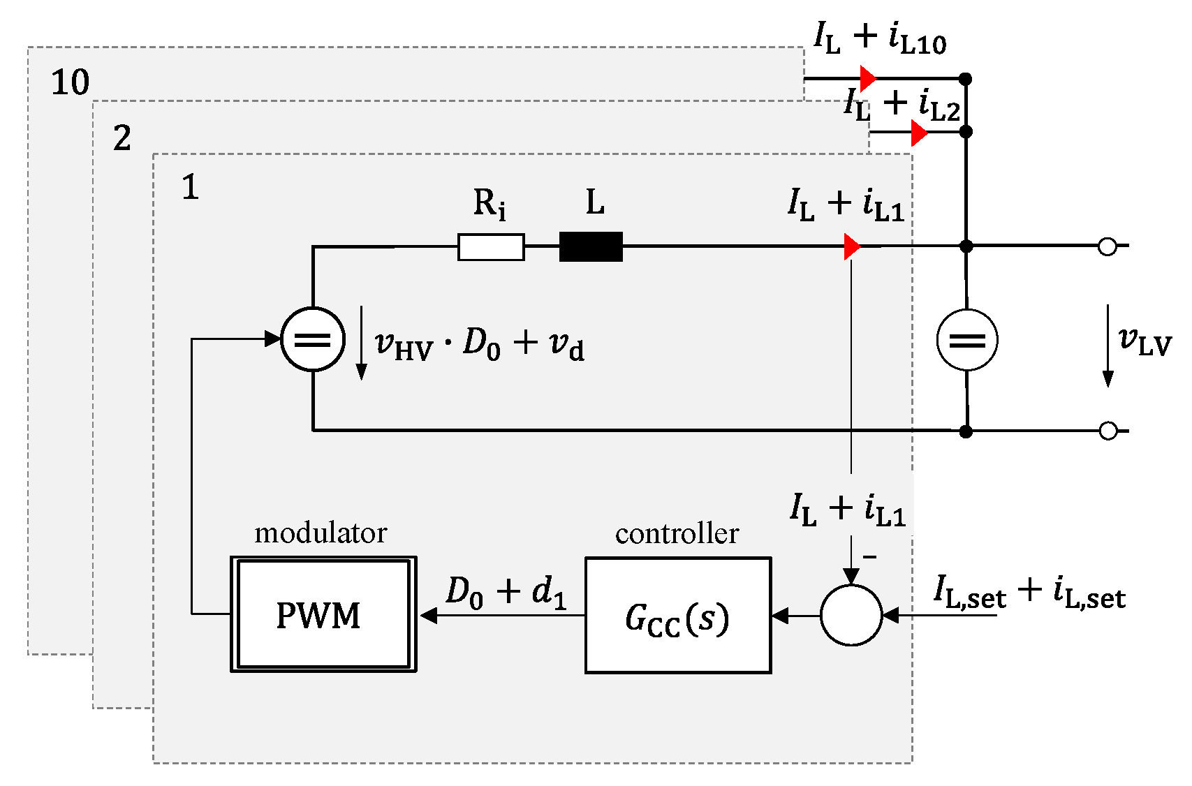
While value discretization only affects digitally controlled converters, time discretization is inherent to any power converter due to its switching actions. To investigate the behavior of PWM on the converter’s transfer function, the simplified model of a 10 phase buck converter’s current control as shown in Figure 2 is used. Each phase is controlled by a current controller G C C —acting on the difference in measured inductor current I L n of phase n to a reference current I L , s e t —with no interaction between the individual controllers. The input and output voltages are set as constant voltage sources to eliminate any interaction between the 10 phases. Therefore, if a small signal perturbation i L , s e t is added to I L , s e t , the perturbations i L , n measured in the individual phases should ideally be describable by the same closed loop transfer function G C L s :
i L n s = i L , s e t s · G C L s
The reason for the 10 phases is the noise cancelation in inductor currents. If all phases are perfectly interleaved, the switching noise in the sum of all i L n should cancel out up to five times the switching frequency. This should allow the investigation of G C L s through simulation even close to and above switching frequency. We will therefore measure G C L s as
G C L s = 1 10 · i L , s e t s · n = 1 10 i L n s
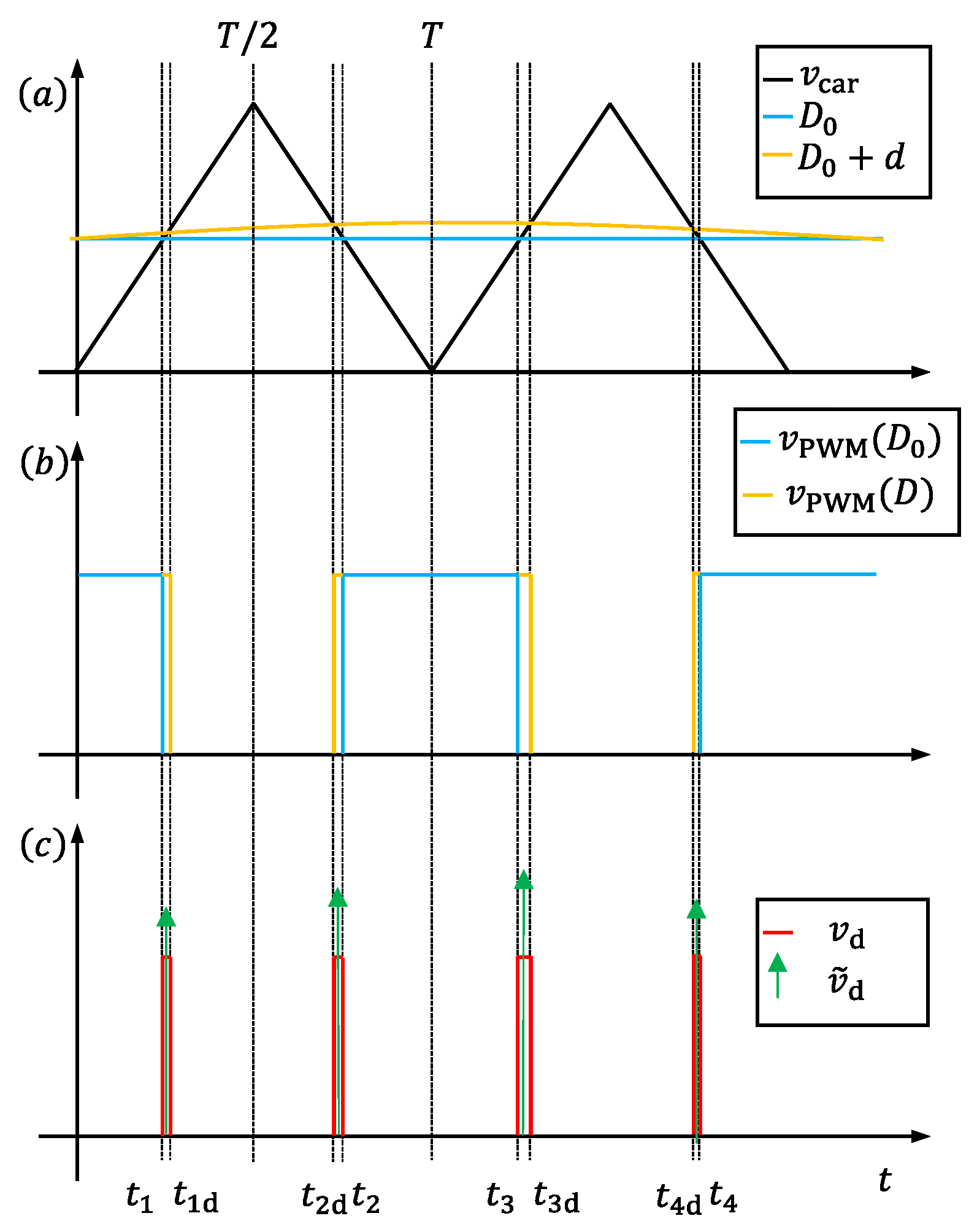
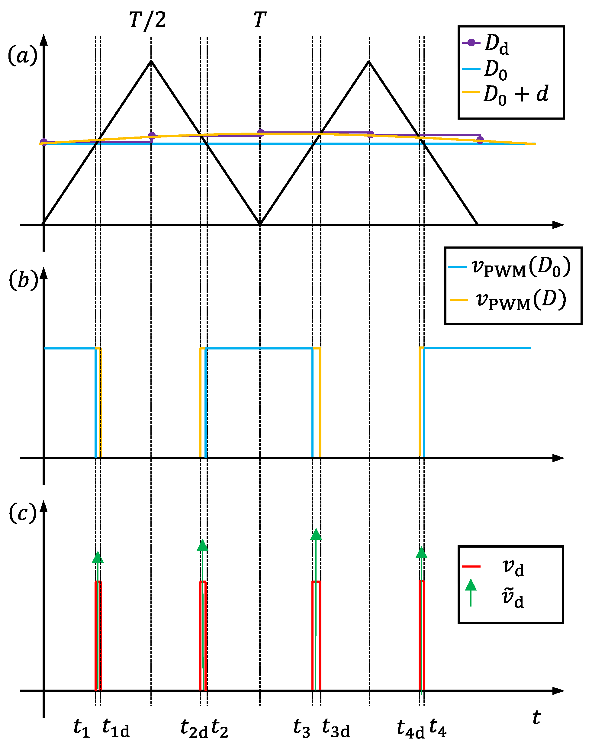
While G C C as well as L and internal resistances R i are all linear time invariant, the influence of the PWM cannot as easily be transformed into the frequency domain. Instead, the effect of the modulator on d , can be explained by using a simplified time variant model shown in Figure 3. Similarly to the small signal perturbation in currents, we can first describe the duty cycle D as a constant operating point dependent on D 0 and a small signal perturbation d :
D t = d t + D 0
To generate the PWM, D is compared to a carrier signal v c a r as shown in Figure 3a. v c a r oscillates between 0 and 1 and is defined by its rising slope v ˙ c a r , r and falling slope v ˙ c a r , f . In this paper, we will assume a symmetric triangular carrier, where v ˙ c a r , r and v ˙ c a r , f normalized in amplitude and time are
v ˙ c a r , r = v ˙ c a r , f = v ˙ c a r = 2
If D is lower than the carrier, then the high side switch is turned on, if D is higher than the carrier, then the low side switch is turned on. This leads to a PWM signal with the amplitude equal to the input voltage v H V . D 0 can be determined by fulfilling the following condition:
D 0 · v H V = v L V + I L · R i
By applying only D 0 to the system, the PWM signal v P W M ( D 0 ) will be observed as shown in Figure 3b in blue. v P W M ( D 0 ) is not a DC signal and will already include the current ripple during unperturbed operation. If a small signal perturbation i L , s e t is applied, the small signal perturbation d will change v P W M ( D 0 ) to v P W M ( D ) as indicated by the yellow PWM signal in Figure 3b. d therefore leads to a perturbation PWM signal v d :
v d t = v P W M D , t v P W M ( D 0 , t )
which is equal to the red PWM signal in Figure 3c.
If like in Figure 3 a triangular carrier signal is used, v d (red pulses in Figure 3c) has twice the frequency of v P W M ( D 0 ) and v P W M ( D ) , since there can be a change in D during turn on and turn off. If instead a sawtooth carrier were to be used, only the time of turn on t 2 n or turn off t 2 n 1 can be perturbed.
For each switching instant, we can define two points in time: t n where the half bridge would switch for D 0 and t n d where the half bridge will switch due to the perturbation. To relate v d to d for a sufficiently low frequency perturbation—i.e., sufficiently lower period than the difference in time between t n and t n d —we can assume for d :
d ( t n d ) d ( t n )
For the high side switch turn off instant (e.g., t 1 ) we can calculate the pulse width τ d of v d by using the slope v ˙ c a r of v c a r and d :
τ d = t 2 n 1 d t 2 n 1 d v ˙ c a r = d 2
For the high side switch turn on the sequencing of t n and t n d is exchanged therefore the pulse width τ d is
τ d = t 2 n t 2 n d d v ˙ c a r , f = d v ˙ c a r = d 2
For a small signal perturbation, we can also assume
t n 1 t n 2 = t n
and approximate the pulses of v d as a series of δ -distributions as indicated by the green arrows in Figure 3c. For both to have the same effect on the inductor current, the only requirement is
T 2 n T 2 n + 1 v H V · d u ˙ c a r · δ i t t 1 d t = T 2 n T 2 n + 1 v d d t
In the time domain, we can therefore describe the PWM signal as v ~ d :
v ~ d t = d t · v H V 2 · n = δ t t n
A small signal model of the plant with the PWM can now be derived, using v ~ d :
i L s = v ~ d s · R i + s L
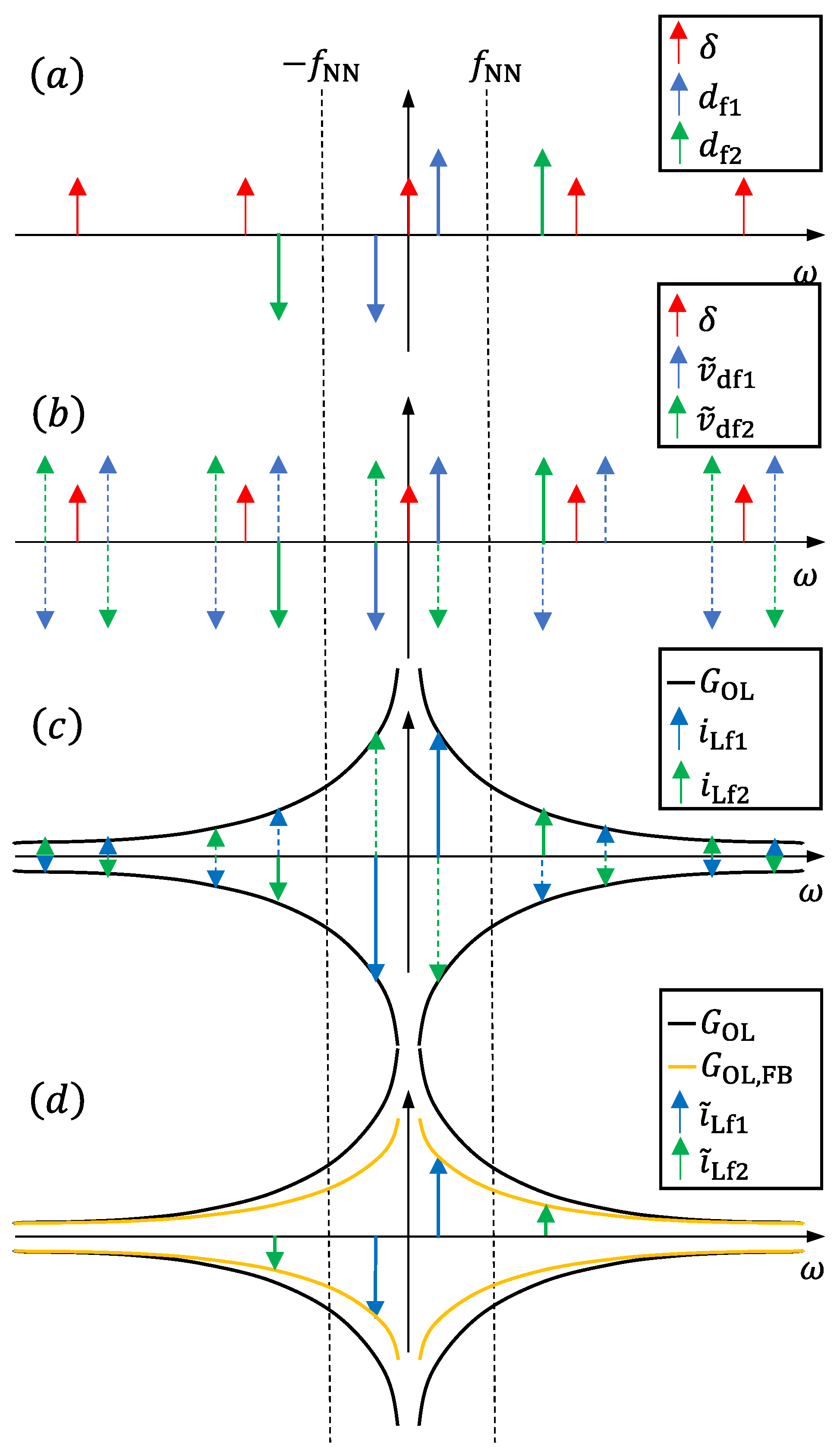
Figure 4 shows the effect of PWM in the frequency domain. By definition, the δ -comb of the PWM stays a δ -comb (red arrows) in the frequency domain. The distance between two δ -distributions is twice the switching frequency. If d is a mono-frequency perturbation, it will be represented as two δ -distributions as indicated by the blue arrows for a perturbation lower than switching frequency and as green arrows for a perturbation above switching frequency in Figure 4a. As v ~ d results are from a multiplication in the time domain, it is a convoluted signal of the δ -comb and the mono-frequency d in the frequency domain. v ~ d f 1 and v ~ d f 2 are caused by the excitations d f 1 and d f 2 and therefore gain additional frequency components as shown by the dashed arrows in Figure 4b.
Since d is a result of the linear controller, its frequency response can be directly calculated into an input signal i L , s e t via G C C :
d s = G C C s · i L , s e t s
The linear open loop transfer function G O L depending on G C C and the converter is therefore given as
G O L s = G C C s · R i + s L
This linear open loop transfer function is shown as the black line—mirrored at the x-axis for negative excitations—in Figure 4c. Consequently, the measurable output current should result from G O L as well as an equivalent transfer function of the PMW modulator G P W M acting on i L , s e t :
i L s = G O L s · G P W M · i L , s e t s
Due to v ~ d f 1 and v ~ d f 2 not being mono-frequency signals, i L also includes other frequency components that are shaped by G O L as shown by the dashed arrows in Figure 4c. Still, if only the original excitation frequency (solid arrows) is considered, the PWM does not have any additional effect. Therefore, if the open loop transfer function is measured, and only the excitation frequency component is evaluated, the PWM transfer function G P W M must be
G P W M s = 1
If the control loop is now closed, one would assume a linear closed loop transfer function G C L , L i n :
G C L , L i n s = G O L s 1 + G O L s
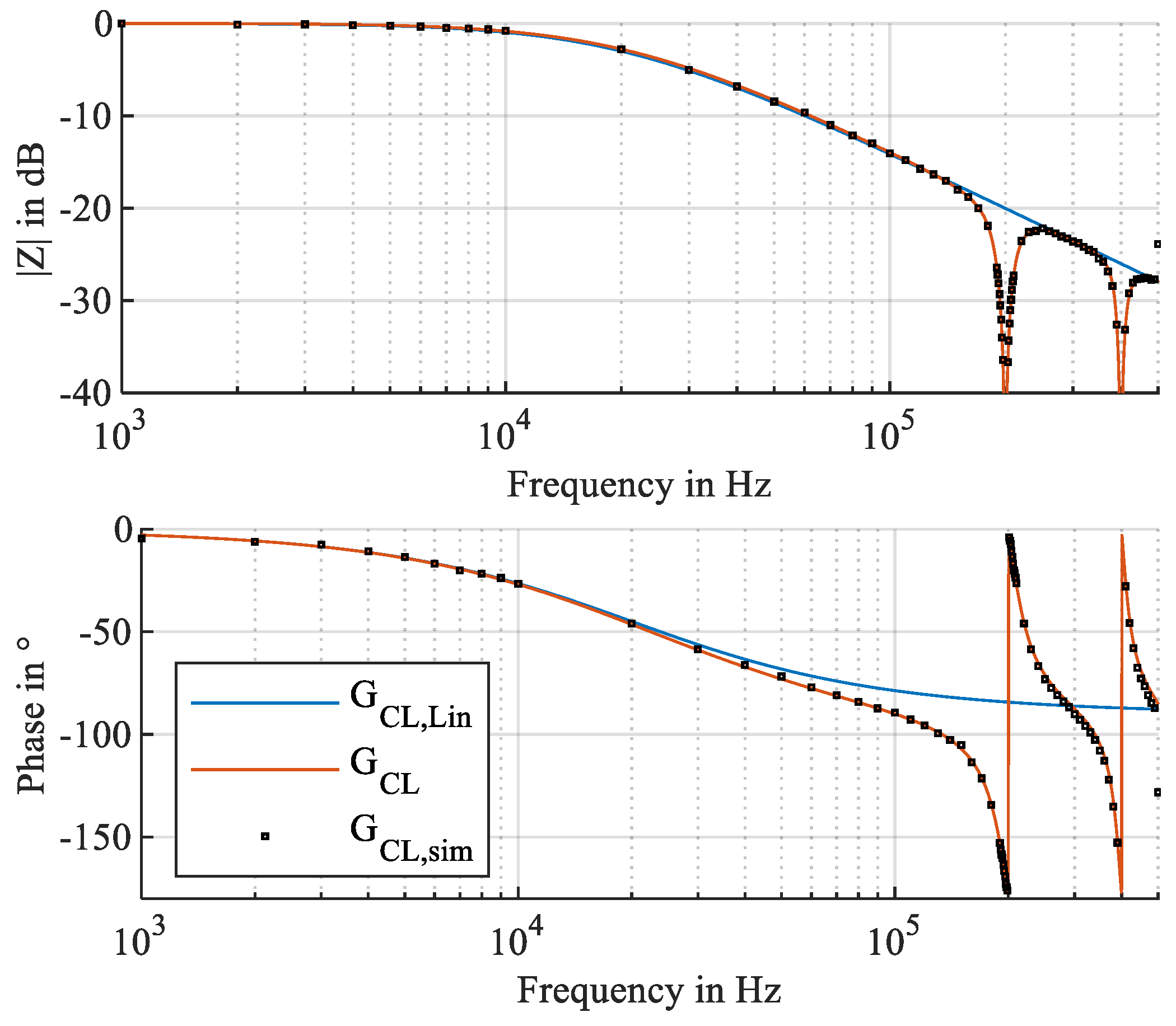
This is not the case, as shown in Figure 5 for a simulation of the 10 phase closed loop current controller at a switching frequency f s of 100 kHz. While the simulated values G C L , s i m show good accuracy with G C L , L i n at lower frequencies, they diverge greatly at twice the switching frequency.
To explain the difference, we need to include the natural aliasing of the PWM. Due to the two times switching frequency “sampling” of PWM, we can define an s 0 as
s 0 = j · 2 π · 2 · f s
This s 0 represents the complex angular frequency associated with the natural aliasing.
Due to the aliasing of the higher frequency components, all high frequency components will lead to aliases at the excitation frequency. The measured i L at the switching actions will be altered to i ~ L as shown in Figure 4d. Therefore, the feedback transfer function G O L , F B needs to account for aliasing:
G O L , F B s = G O L s + n = 0 G O L s n + G O L s n with s n + = n · s 0 + s s n = n · s 0 s
The true closed loop transfer function G C L , as plotted in Figure 5, therefore needs to be calculated as
G C L s = G O L s 1 + G O L , F B s
G C L s now accurately represents G C L , s i m until the onset of switching noise at 500 kHz obscures the measurement.
Interestingly, if G O L can be estimated as an integrator with a constant gain of K ,
G O L s = K s
which can be a good estimation for a buck converter with well-tuned PI-control, using the partial fraction decomposition of the cotangent, G C L can be simplified to
G C L s = K s 1 + K cot s s 0
We can therefore interpret f s as the natural Nyquist frequency f N N of the converter, if a symmetrical carrier is used and D 0 is close to 0.5. If a sawtooth carrier is used, there will be only one δ -distribution per switching frequency, leading to an f N N of half of f s :
f N N = 1 2 f s
If a symmetrical carrier is used and D 0 is close to 1 or 0, the δ -distributions will be so close that they can be interpreted as a single δ -distribution, again leading to an f N N of half of f s .
If digital control is used, the ADC samplings will typically not coincide with the switching actions. This is shown for a digital sampling frequency f s a m p of twice the switching frequency in Figure 6. The sampling happens at half the switching period T and multiples thereof. At these points, the digital duty cycle D d is sampled from an analog signal consisting of an offset D 0 and the perturbation d as indicated in Figure 6a. Since the switching actions are not at multiples of T / 2 , there is a time delay between sampling and the converter’s action as shown in Figure 6a–c. In this case, the transfer functions need to be adjusted for a delay of τ 11 for turn off, or τ 12 for turn on.
Regarding aliasing, the effect of digital sampling on the actual Nyquist frequency f N depends on the switching frequency and the sampling frequency. For the digital sampling, a Nyquist frequency f N d exists, which is half of f s a m p . As explained before, the PWM introduces its own natural Nyquist frequency f N N . Here, two cases can be distinguished. Either f N d is as high or higher than f N N , or f N d is lower than the converter’s f N N . In the first case, the digitally controlled converter’s Nyquist frequency f N will be equal to f N N . This can be intuitively seen, as an infinite sampling frequency would reproduce the analog control, with the delays τ 11 and τ 12 approaching zero, as f s a m p is further increased. The effect will be visible in the transfer function but will not affect the measurement with wide band width signals. In the latter case f N will be equal to f N d , since the sampling and therefore aliasing of the ADC will dominate.

3. Wide Bandwidth Measurement System

The most straight forward approach to impedance measurement is using mono-frequent sinusoidal signals. To obtain a full frequency spectrum, selected frequency points are measured individually, with a fine-tuned bandpass filter acquiring only the relevant frequency component of the current and voltage waveforms. Requirements for mono-frequency coupling are given in [8].
To probe a wide frequency range in small frequency steps, measurement of mono-frequent signals takes a considerable amount of time, since the system should be at a steady state during measurement. The test signal must therefore be held at the same frequency for considerably longer, than the lowest time constant τ m i n of the to be investigated system [41]. The measurement time t m e a s of n successive frequencies will correspondingly increase. Also, the total test signal energy E m e a s as a product of measurement time and the average test signal power P t e s t increases accordingly:
E m e a s > τ m i n · n · P t e s t
If instead PRBS are used, the measurement time can be greatly reduced [8,24,25,26,27,28,29,30,31,32,33,34,35,36,37,38,39,40,41]. To be able to measure a converter, a system capable of injecting PRBS-shaped currents into a grid, as shown in Figure 7, is developed. The PRBS is coupled by turning a transistor on and off, based on the digital PRBS signal d P R B S . For a given DUT voltage v D U T , the power resistor R C adjusts the amplitude of the coupled current i P R B S :
i P R B S t = v D U T R C · d P R B S t
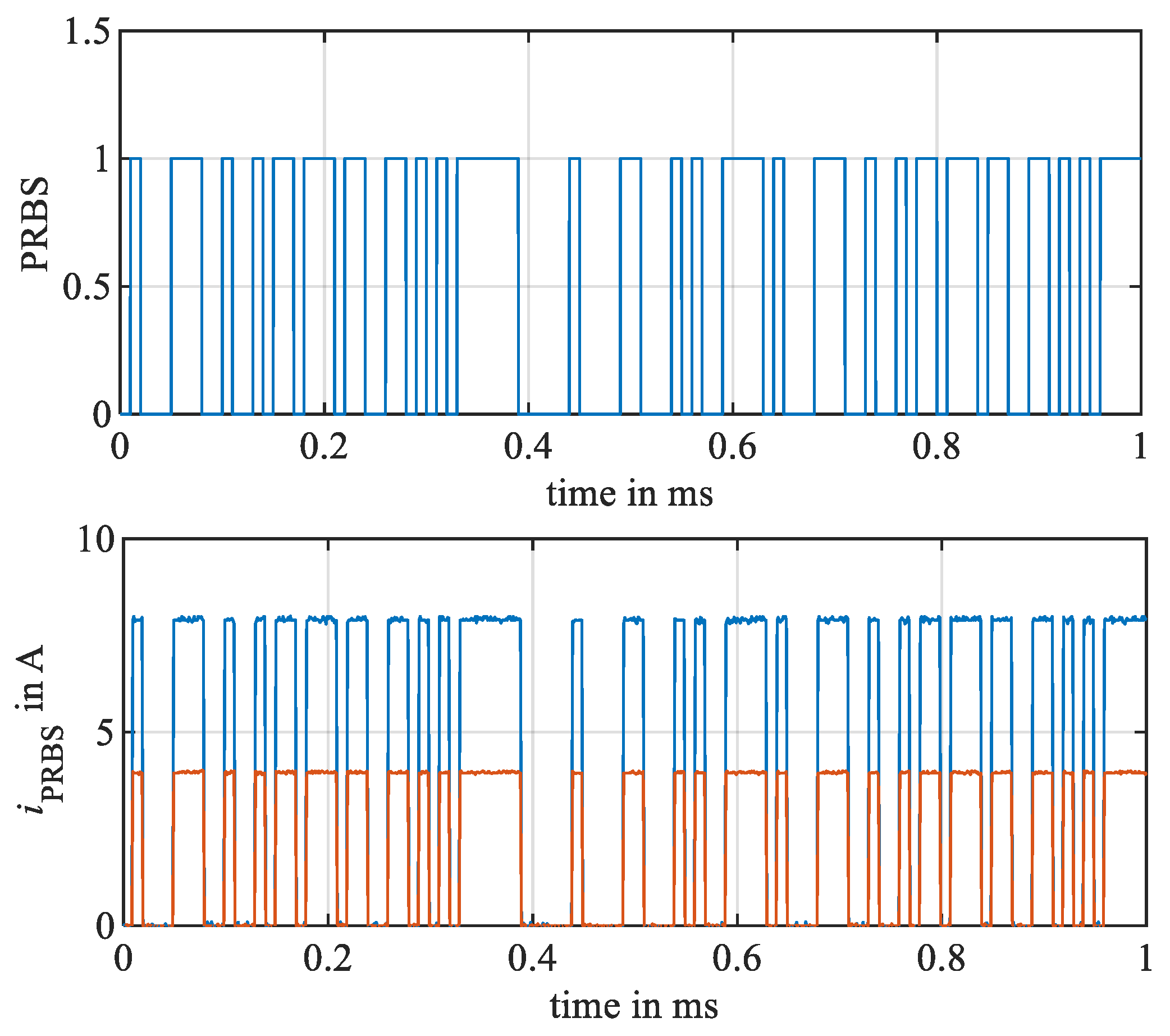
Two currents with different amplitudes corresponding to the same digital PRBS are shown in Figure 8. i P R B S therefore has the same spectral components as the PRBS. Different from coupling methods using power converters, the shape of i P R B S is not impacted by control dynamics.
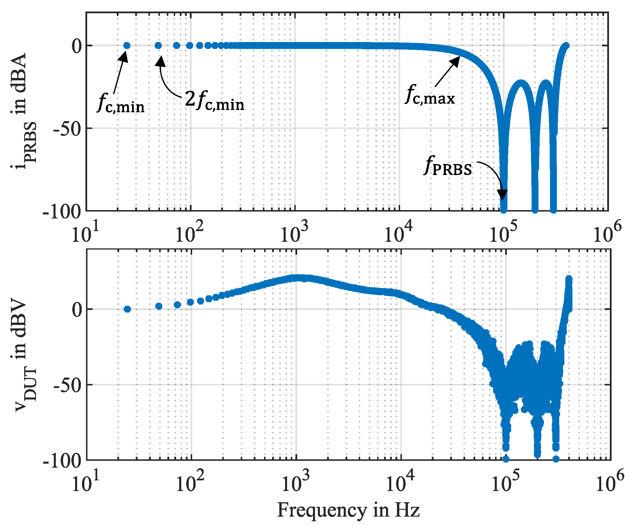
The PRBS itself is characterized by two frequencies. Depending on the order O of the PRBS as well as the bit-length t b , a minimum coupling frequency f c , m i n can be selected:
f c , m i n = 1 t b · 2 O 1
The simultaneously measured frequencies f c , n are multiples of this minimum coupling frequency:
f c , n = f c , m i n · n
The maximum usable frequency f c , m a x also depends on the bit-length t b . From this t b , a characteristic frequency f P R B S can be calculated:
f P R B S = 1 t b
f c , m a x is then usually set at the frequency where the amplitude of the excitation has decreased to −3 dB:
f c , m a x f P R B S π
An exemplary measurement of i P R B S and the resulting v D U T is shown in Figure 9.
To estimate the DUT impedance Z D U T as well as a possible connected source/load impedance Z S / L , the DUT voltage v D U T as well as the currents i P R B S , i D U T , and i S / L are measured. To minimally perturb the system when turned off, i D U T and i S / L are measured with magnetic current sensors, while i P R B S is measured through a shunt resistor. This overdetermination in the current measurement allows for a compensation of the current sensors’ transfer function G C S . Since the measured currents i D U T , m and i S / L , m include the G C S as well as i D U T and i S / L respectively,
i D U T , M = i D U T , M · G C S
i S / L , M = i S / L · G C S
G C S can directly be calculated from measurement:
G C S s = i D U T , M s + i S / L , M ( s ) i P R B S s
Therefore, a measured i D U T , M can be translated into the actual i D U T with
i D U T s = i D U T , M s i P R B S s i D U T , M s + i S / L , M ( s )
To obtain high vertical resolution, all signals are sampled with a 16-bit ADC. Since the voltage measurement suffers from the high DC-offset, all measurements are high-pass filtered with a corner frequency of 10 Hz. To avoid aliasing, the signals are also second-order low-pass filtered with a corner frequency of 50 kHz and sampled with 400 kHz. The reason for using the same bandpass G B P s for all signals is that no calibration is needed for the impedance calculation:
Z D U T s = v D U T s · G B P s i D U T s · G B P s = v D U T s i D U T s
A detailed description of the components used in the measurements system are given in Table 1. Errors and tolerances are taken from the datasheet values.
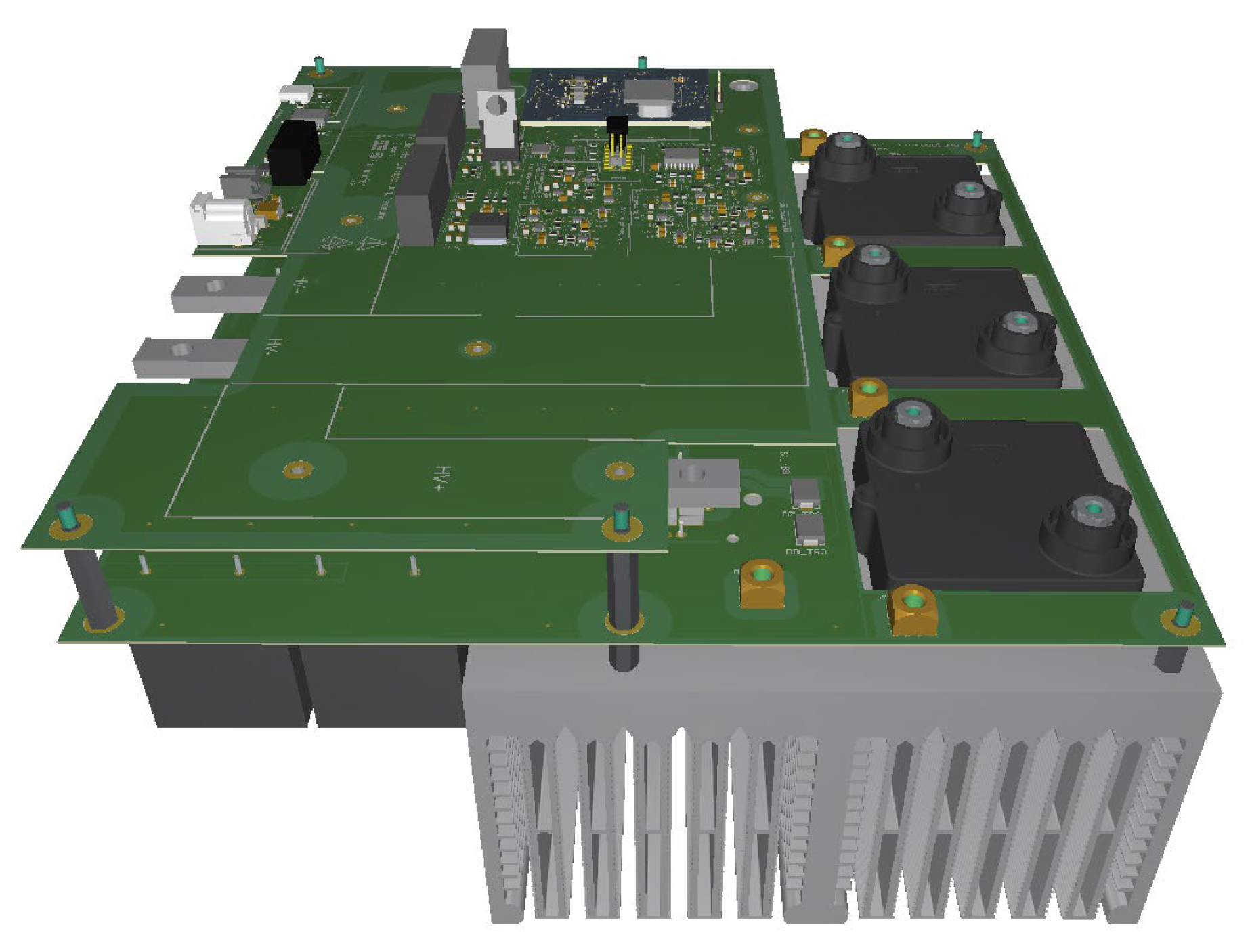
The 3D model of the physical measurement system is shown in Figure 10. The system includes 3 resistors (50 Ω, 100 Ω, and 200 Ω) to allow for different excitation amplitudes as shown in Figure 8 for 50 Ω and 100 Ω. The losses in R c are absorbed in an aluminum heat sink. During active measurements, the heatsink operates mostly like a thermal storage unit. Since aluminum has a high thermal capacitance, even 1 kg of heatsink can absorb 70 kJ for an allowable temperature rise of 80 K. The dissipated energy of a PRBS pattern with a length of 16 , 383 bits (an order O of 14) and f P R B S = 100 kHz repeated 50 times at an amplitude of 10 A only introduces 16.4 kJ intro the heatsink. Here, the benefit of wide bandwidth measurement becomes directly apparent. With the whole frequency band measured simultaneously, the heat absorption can be scaled for f c , m i n instead of n times f c , m i n . Continuous mono-frequency sweeps would require continuous cooling in the kW range, if dissipative measurement were to be used instead.

4. Simulation Results

To evaluate the effect of the wide bandwidth measurement system on a power converter, simulation models of the system shown in Figure 11 are set up. The model represents a bidirectional droop controlled buck converter with a variable output capacitance C D U T and a stepping-down voltage of 1 kV to 500 V. The converter is kept in continuous conduction mode, since it behaves linearly under load current variations. This allows direct comparisons of different amplitude measurements, despite the changes in operating point currents due to variations in i P R B S .
To model both value and time discretization independently, the converter is firstly modeled to only include the value discretization and then with only with time discretization. Both effects can therefore be accounted for separately. Different from [8], the excitation is simulated for the realistic measurement system as shown in Figure 11.

4.1. Value Discretization

To overcome value discretization, the voltage measurement needs to flip by at least one bit. The corresponding voltage for this bit-flip can be defined as Δ v L S B . As investigated in [8], a logic “1” of the PRBS leads to a charge Q C displaced from the grid side capacitances C D U T and C S / L of both the DUT and a source/load converter. For the resistive coupling, this Q C can be calculated as
Q C = t t + t b v D U T t ~ R c d t ~
Assuming v D U T to be sufficiently constant during the measurement, (35) simplifies to
Q C = v D U T R c · t b
For Q C to flip one bit of the ADC, the following condition must hold:
Q C Δ v L S B · C D U T + C S / L
Knowing the desired f P R B S , the required amplitude of i P R B S can be calculated as
i P R B S = Q C · f P R B S
The required R c can then be determined from i P R B S and v D U T :
R c = v D U T i P R B S
To investigate the effect of the ADC a value quantization of 125 mV—resembling the resolution of a 12-bit ADC at 500 V—is introduced into the voltage measurement. The parameters for the converter are selected to match the experimental prototype in Section 5 and are given in Table 2. To avoid any time discretization effects, the converter is modeled as an average switch model, thereby eliminating the effects described in Section 2.2.
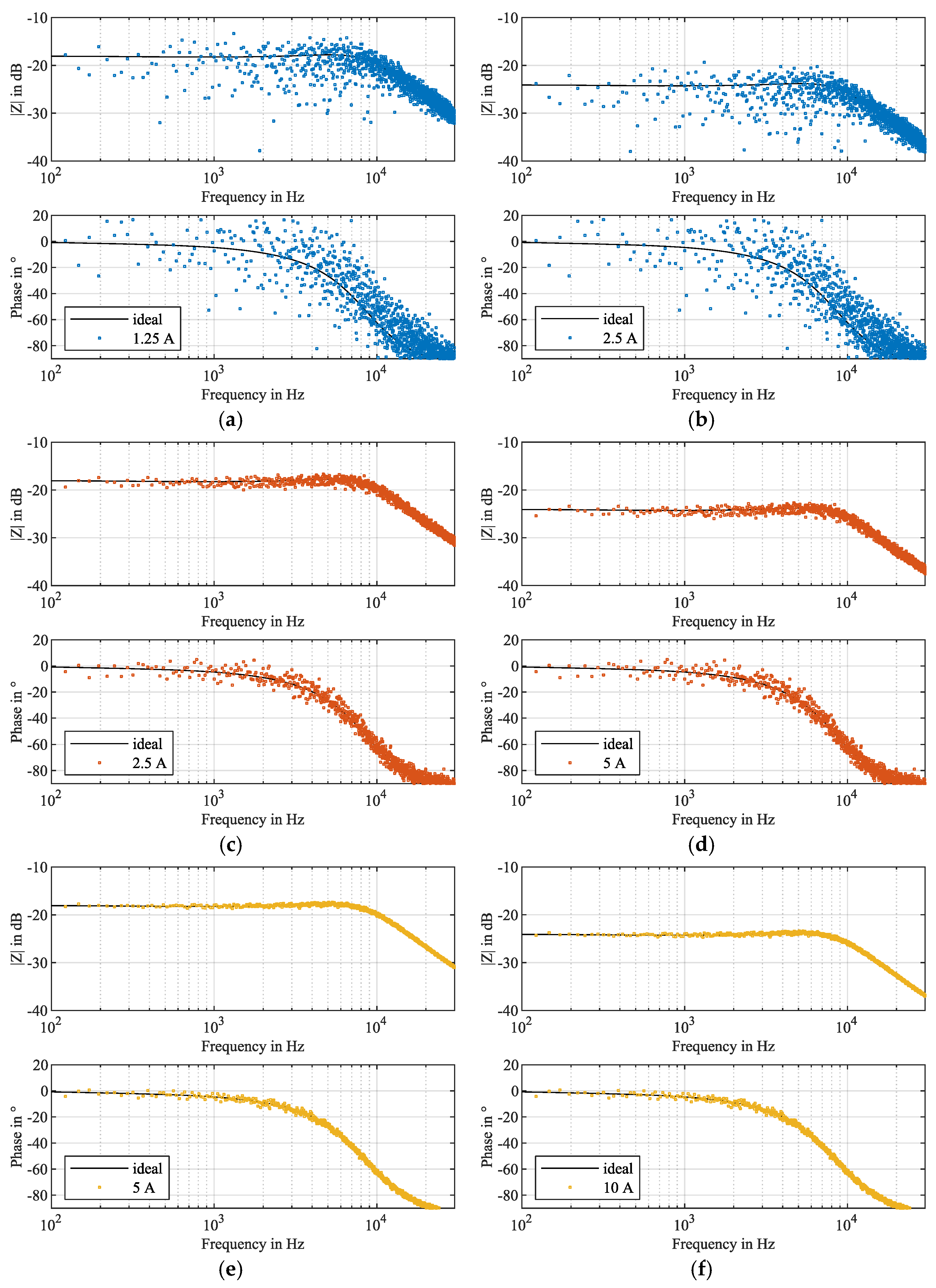
To investigate the generalizability of Equation (38), the converter is simulated with two different output capacitances of 400 μ F and 200 μ F . To reach a stationary operating point, a PRBS with an O of 12 and an f P R B S of 100 kHz ( t b of 10 μ s ) was repeated 100 times. The in-simulation sampling frequency was set to 1 MHz to avoid aliasing effects. This allows measurement up to a frequency of 30 kHz and would require an i P R B S of 2.5 A for 200 μ F and 5 A for 400 μ F according to Equation (38).
To investigate the effect of different amplitudes, the different R C values are applied in simulation. For the 200 μ F   C D U T , the resistance values were set to 400 Ω, 200 Ω, and 100 Ω, leading to currents of approximately 1.25 A, 2.5 A, and 5 A. The 400 μ F   C D U T was perturbed with 2.5 A, 5 A, and 10 A resulting from an R c of 200 Ω, 100 Ω, and 50 Ω. To result in the same corner frequency, the droop resistance was set to 125 mΩ at 200 μ F and 62.5 mΩ at 400 μ F . In Figure 12, the 200 μ F results are shown on the left (a, c, e) and the 400 μ F results on the right (b, d, f).
Not only do the results show that the noise greatly decreases once the threshold in Equation (38) is met, but also that the two scenarios behave identically in simulation. Aside from the reduction in gain by 6 dB, the 200 μ F and 400 μ F cases not only show the same trend in noise, but the deviations from the ideal measurement are also exactly identical for both, if the ratio of Q C to C D U T remains the same. Additionally, the signal to noise ratio not only improves at higher frequencies, but also at low frequencies, once Equation (38) is met. This indicates a frequency independence of SNR in terms of amplitude quantization. If a series of mono-frequency measurements were to be made, this would be different, since Q C would be lower for higher frequencies.
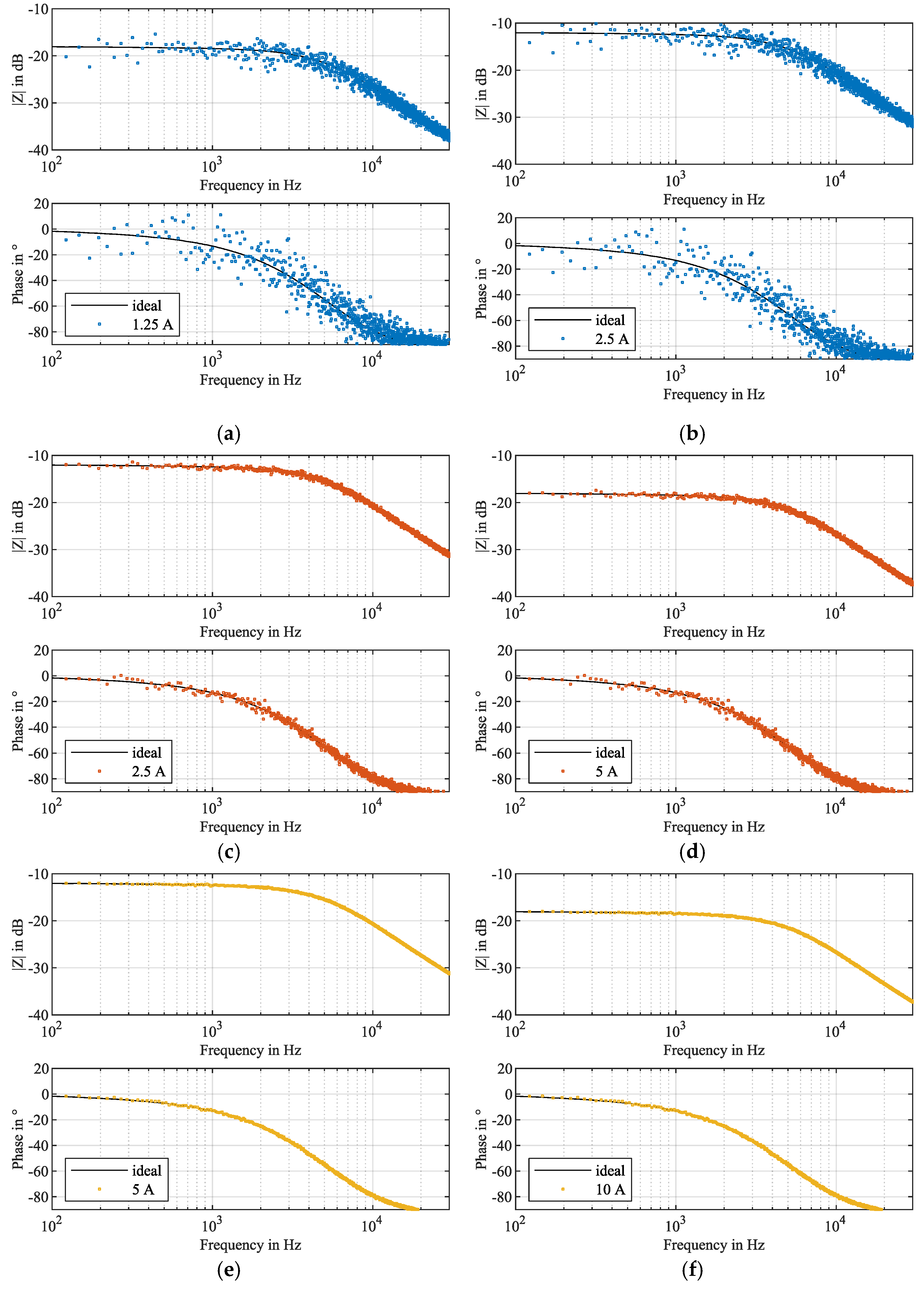
To observe the converter with change dynamics, the two simulations were repeated with changed droop resistances. For both the 200 μ F and 400 μ F   C D U T , the droop resistances were doubled to 250 mΩ and 125 mΩ, respectively. The results are shown in Figure 13.
Similarly to the lower droop resistance simulations, the requirement given in Equation (38) can be interpreted as a threshold for proper measurement. Compared to Figure 12, the simulation results in Figure 13 generally show lower noise. This can be explained by the reduced dynamics of the system. With the increased droop resistance, the impedance of the converters modeled exhibits a −3 dB corner frequency of approximately 5 kHz, whereas the lower droop resistance leads to a corner frequency of 11 kHz.
The effect of converter dynamics can be approached by taking the two most extreme cases. In the most dynamic case, the converter would have infinite dynamics leading to an SNR of 6.02 dB, as given by the dynamic range of a 1-bit analog to digital conversion, when Equation (38) is met. In the least dynamic case, the converter would have no dynamics and its impedance would be represented only by the analog output capacitor. In this case no quantization would occur. Equation (38) is therefore the limit, where an SNR of more than 6.02 dB can be obtained in any case, with SNR increasing with decreasing dynamics.
In terms of required power to correctly measure the system, the PRBS current does not need to be drastically increased over a mono-frequency signal to properly excite the ADC. Using Equation (38) to estimate the RMS current required to measure at 30 kHz, a purely sinusoidal signal of 3.3 A would be needed. Using PRBS signals therefore greatly reduces the total signal energy for a full spectrum measurement.

4.2. Time Discretization

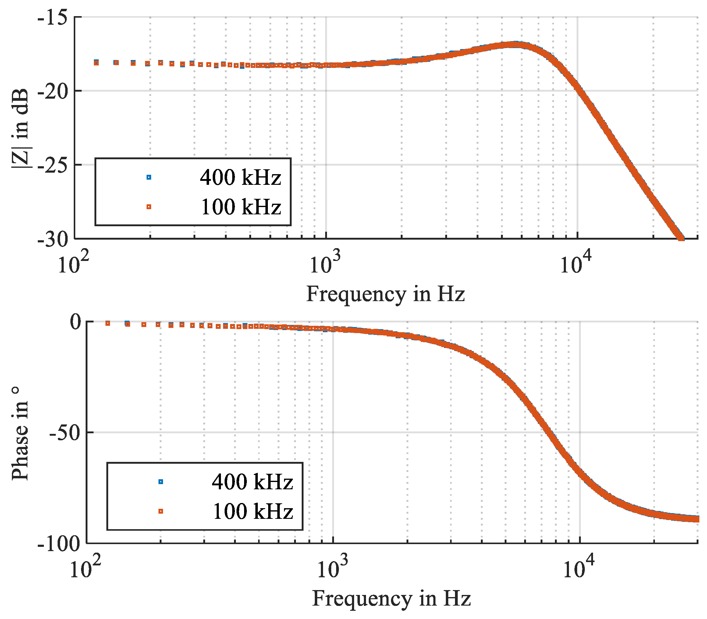
Different than with value discretization, the time discretization of the converter itself impacts the output impedance inherently. As explained in Section 2, high frequency harmonics of the converter can directly impact the closed loop current transfer function. For the simulation model, a comparison of an averaged model with a switched model will therefore never lead to the same results. Instead, a single-phase model of a buck converter is implemented in simulation and tested at different values of f P R B S . The converter is still droop controlled, with a droop resistance of 125 mΩ converting from 1 kV to 500 V. The switching frequency is set to 100 kHz with a triangular carrier-based PWM modulator. For the analog controlled model, this leads to a Nyquist frequency f N N of 100 kHz. The system is then excited with an f P R B S = 100 kHz PRBS with an O of 12 and a f P R B S = 400 k H z PRBS with an O of 14. Both PRBSs show an f c , m i n of 24.2 Hz and are repeated 20 times to assure steady state conditions in simulation. The roll-off frequency f c is at roughly 30 kHz for the 100 kHz PRBS and 120 kHz for the 400 kHz PRBS.
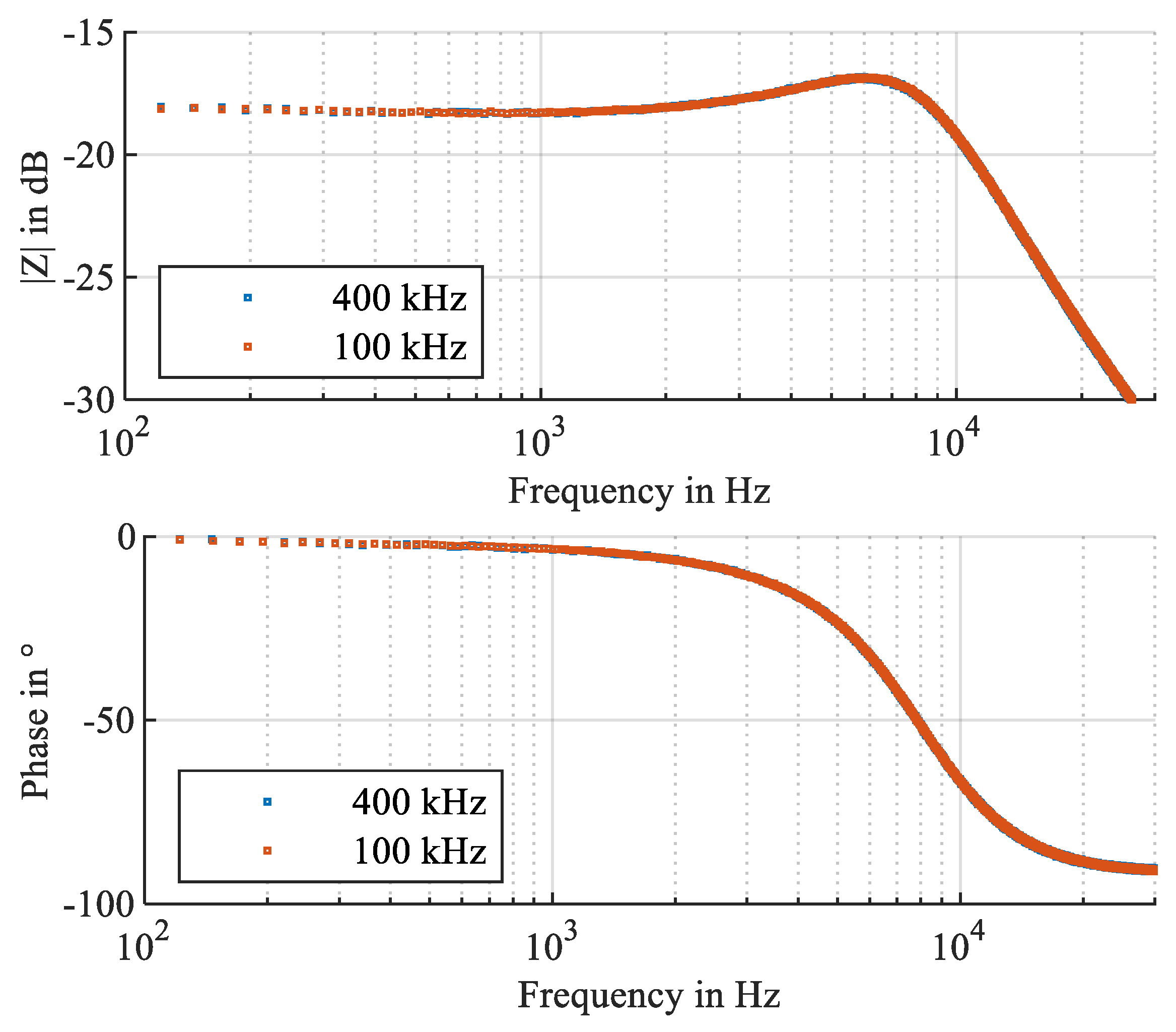
The simulation results for the pure analog control are shown in Figure 14. The lack of difference between the two measurements can be explained by the high damping of the to be aliased frequency parts. At 100.019 kHz, which would be the first frequency misinterpreted by the PWM modulation as 99.994 kHz, the output impedance is already dominated by the capacitor, which leads to the negligible effect of f P R B S . Higher misinterpreted frequencies, affecting frequencies where the control of the power converter dominates, are additionally filtered by the output capacitor, due to i P R B S being a current type signal. The frequency components at 190 kHz, which would affect the measurement at 10 kHz, are already damped by over 25 dB.
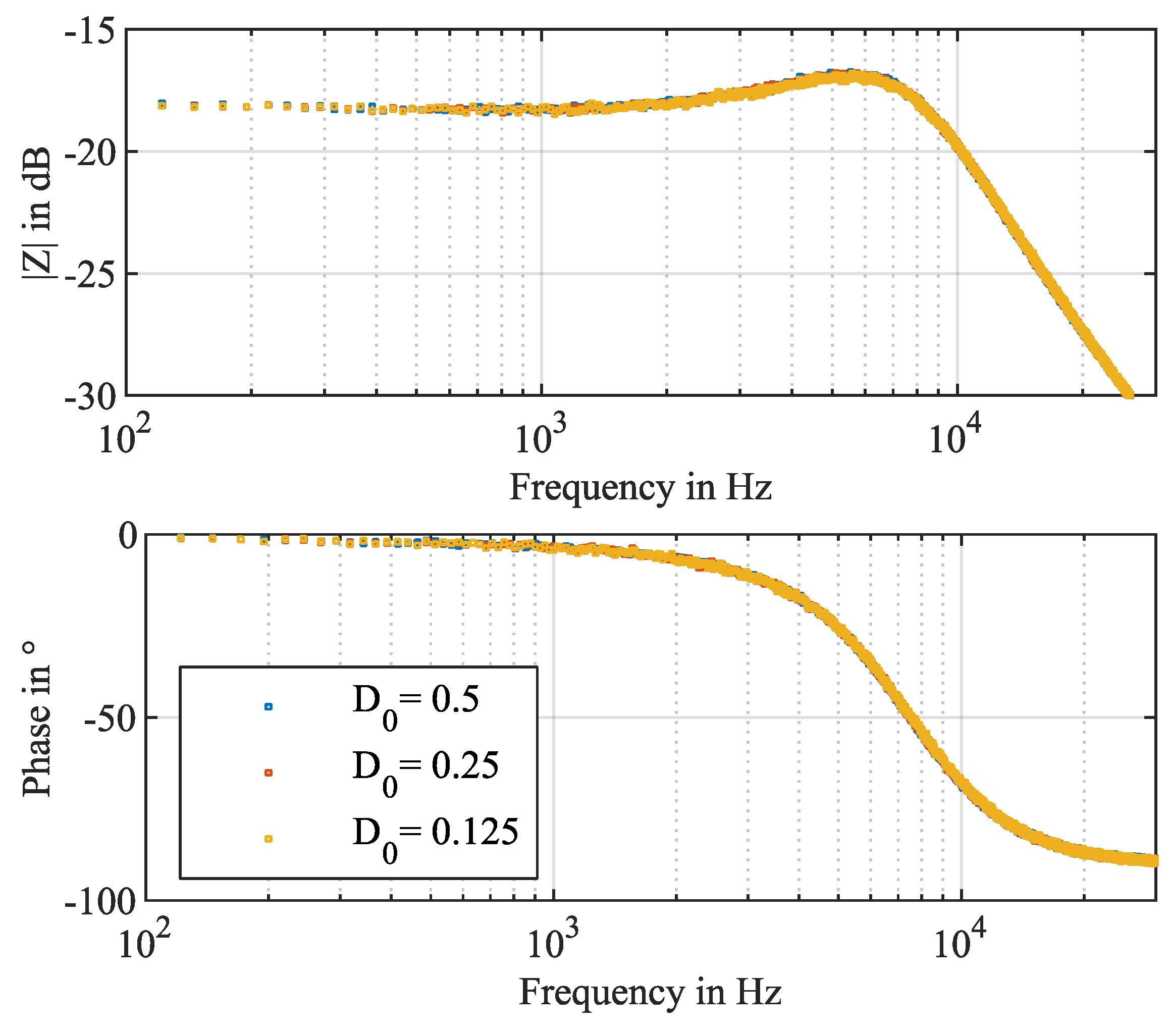
To investigate the behavior at different duty cycles, the output voltage was varied to measure the system under a D 0 of 0.5, 0.25, and 0.125. As shown in Figure 15, D 0 has an almost negligible impact on the noise level of the impedance measurement. Due to the linearity of the buck converter, the change in output voltage also does not impact the impedance shape. For the following investigations, D 0 will therefore be kept to 0.5.
If the converter is instead digitally controlled, the sampling frequency of the control can impact the aliasing. In simulation, the digital control is modeled through sampling and acts on the digital equivalent of the analog control. In this case, the vertical ADC resolution is quasi-infinite and—like with the simulated analog control—only limited by the floating-point resolution of the simulation. The results for time discrete sampling with 200 kHz are shown in Figure 16. Aside from a slight deviation in phase at 20 kHz, the result resembles that of the analog control. While the digitally introduced delay between sampling and switching changes the output impedance, the Nyquist frequency stays the same, resulting in the same negligible effect of f P R B S on the measurement.
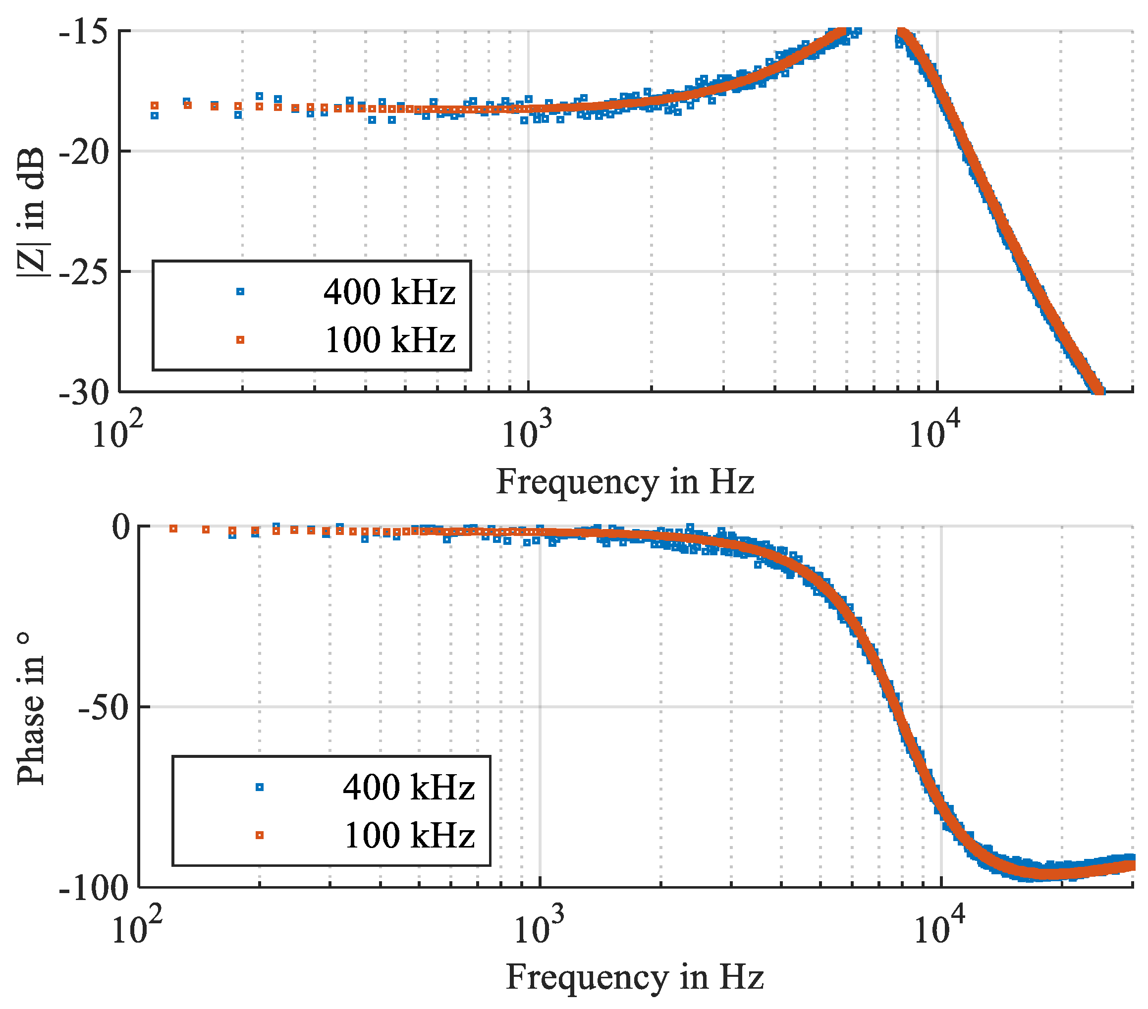
If the sampling frequency is reduced to 50 kHz as shown in Figure 17, the introduced delay has a clearly visible effect on the output impedance. The formerly passive converter now clearly violates passivity at frequencies above 12.5 kHz. Additionally, application of a 400 kHz PRBS (blue dots) now leads to a clearly deteriorated measurement, with increased noise in gain and phase. Still, the effect is mild compared to under-excitation of the ADC for the examined converter.
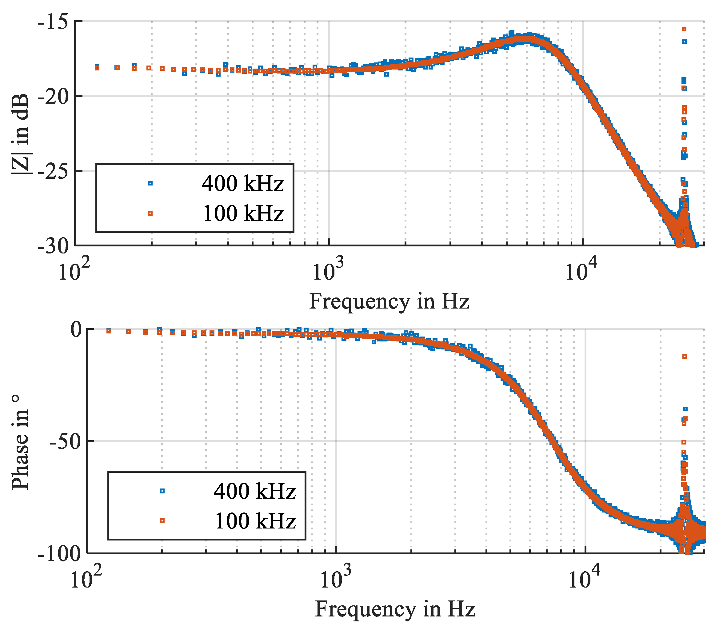
It is important to note that the effect of aliasing in wide bandwidth measurements is not unique to digital control, as shown for an analog controlled converter in Figure 18. Here, the control parameters were left unchanged but the switching frequency was reduced to 25 kHz. While the effect on the shape of the output impedance—aside from artifacts at switching frequency—is not as prominent as with digital under-sampling, the deterioration of measurement of the 400 kHz PRBS (blue dots) compared to the 100 kHz PRBS measurement (red dots) is still clearly visible.
When compared to value discretization, the effects of time discretization are comparatively small, since even the worst-case effects of time discretization (Figure 17) do not replicate only meeting the charge requirement in Equation (38) (Figure 12 and Figure 13). For a synchronous buck converter, it can therefore be surmised that time discretization only has a very limited effect. It is important to note that this might not be true for any topology. Time discretization should therefore be at least kept in mind when selecting f P R B S .

5. Measurement Results

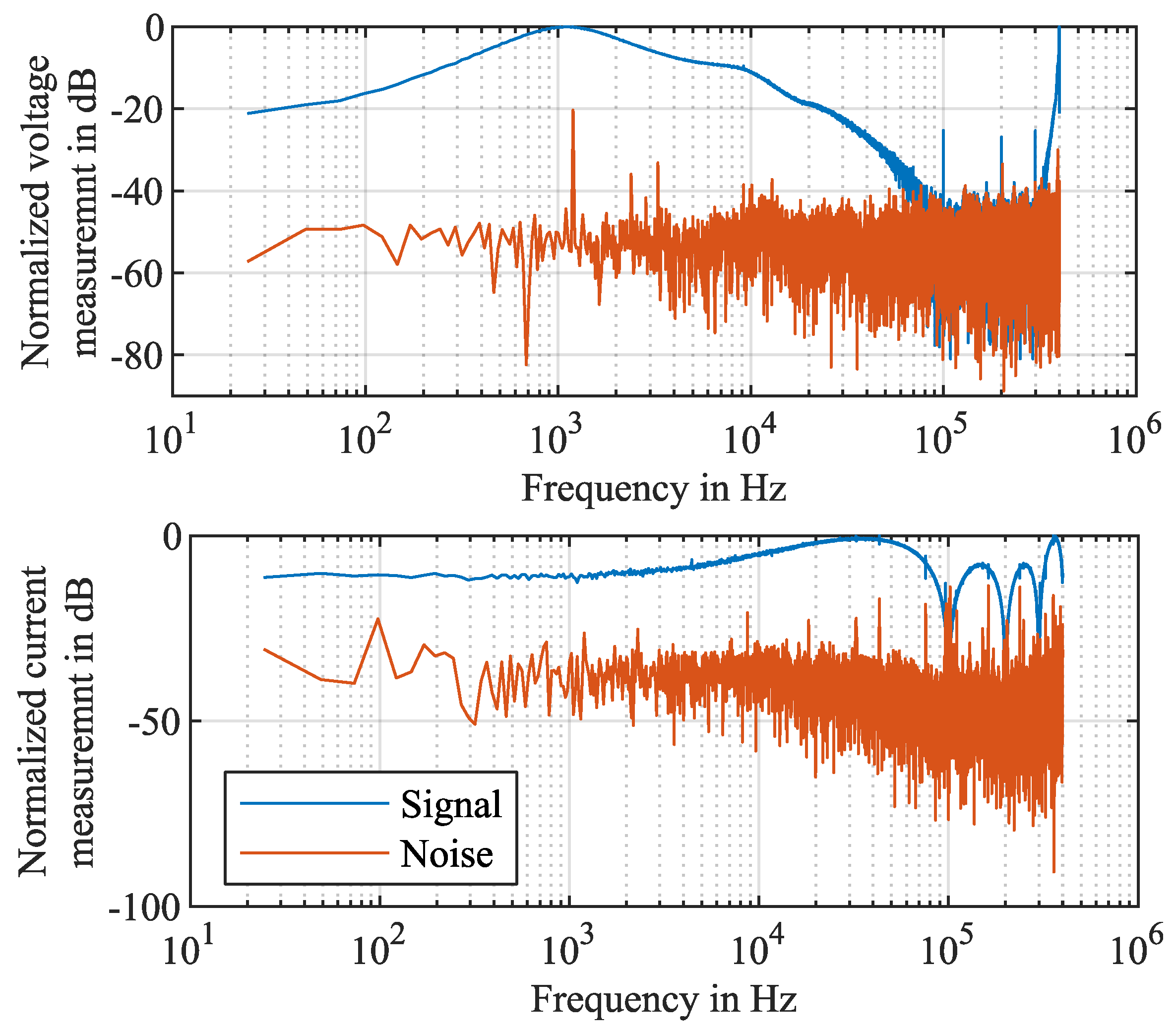
To verify the simulated findings in practice, a digitally controlled synchronous buck converter is measured using the system described in Section 3. The converter is controlled by a cascaded voltage and current control using 12-bit ADCs to convert currents and voltages. The discretization in output voltage measurement is 195 mV, which—together with the output capacitance of 200 μ F —leads to a required Q C of 39 μ C . The converter has a switching frequency of 60 kHz, with the inductor current and input and output voltage sampled four times each switching period, leading to an effective f N d of 60 kHz. The measurement system excites the converter with 25 repetitions of a 100 kHz PRBS with an O of 12. To properly excite the system, a 4 A i P R B S is coupled with a 100 Ω R c at 400 V. The converter parameters are identical to the simulation model in Section 4.1. An exemplary current and voltage measurement, normalized to the maximum signal amplitude, is shown in Figure 19. Due to the 25 repetitions, the measurement includes 24 unusable frequency points for every PRBS constituent frequency. Since the measurement system does not induce any signal at these frequency points, they can be used as a measure of noise. As clearly visible in Figure 19, the noise has no noticeable impact in the frequency range up to 60 kHz. The system will be assumed unperturbed by noise up to 30 kHz with high confidence.
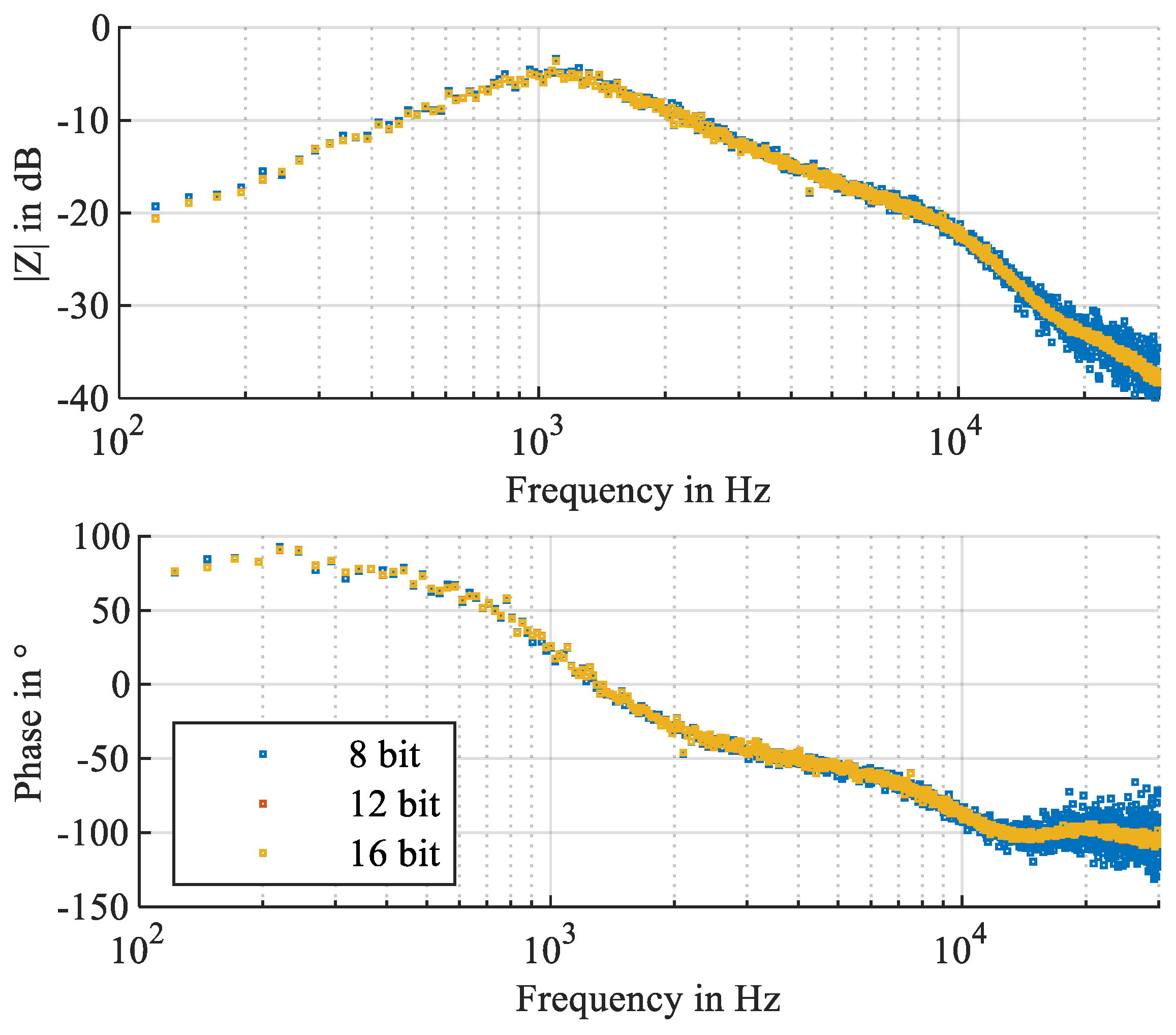
To eliminate misinterpretation of effects due to insufficient excitation of the measurement system’s 16-bit ADC, the 4 A measurement raw data was retroactively reduced to 12-bit and 8-bit resolution as shown in Figure 20. While an under-excitation of the measurement system’s voltage ADC is highly unlikely for signals that can be picked up by the converter’s ADC, an under-excitation in the current measurement could still lead to a deteriorated measurement. As can be seen in Figure 20, only a reduction to 8-bit leads to a noticeable change in the measurement. We therefore conclude that a reduction in signal amplitude up to a factor of 16 would not negatively impact the measurement, when only considering the measurement system.
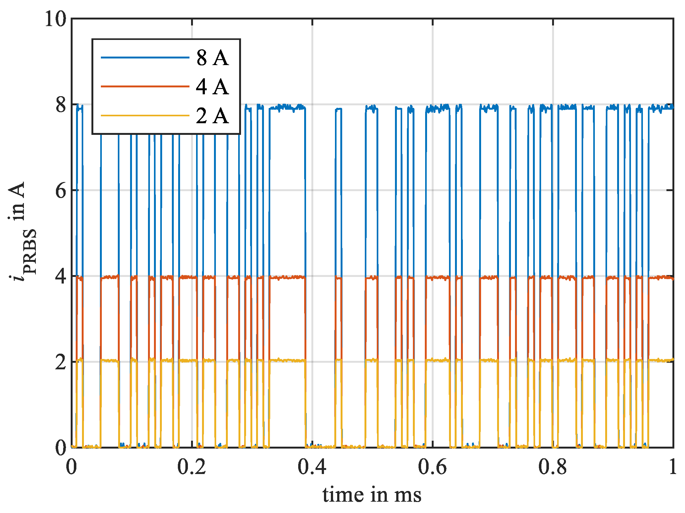
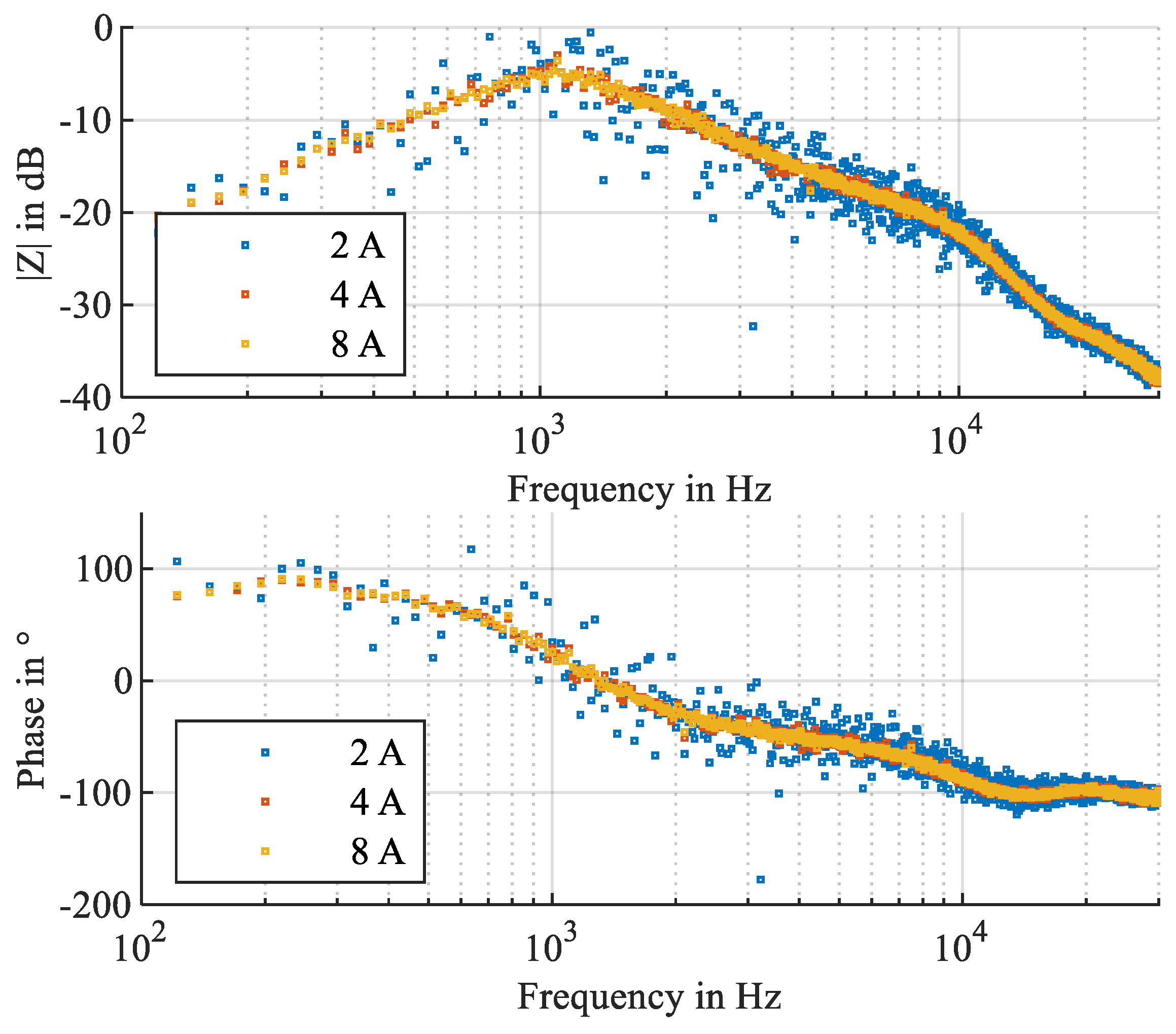
To investigate the influence of the digital control on the system, the measurement is carried out again with a 2 A and an 8 A i P R B S . The injected currents are shown in Figure 21. The results are shown Figure 22. While the increase in signal power to 8 A only marginally improves the measurement, the decrease in i P R B S to 4 A drastically limits the usability of the measurement, validating the stimulatory findings.
Regarding aliasing, no improvement was found if f P R B S was changed to 60 kHz, further indicating the low impact of aliasing on buck converters. It is important to note that this has to be expected of a well-designed digital control system, since perturbations in realistic environments will typically be wide band. A power converter not being able to handle multiple frequency components at once will therefore exhibit unpredictable behavior in a DC grid.
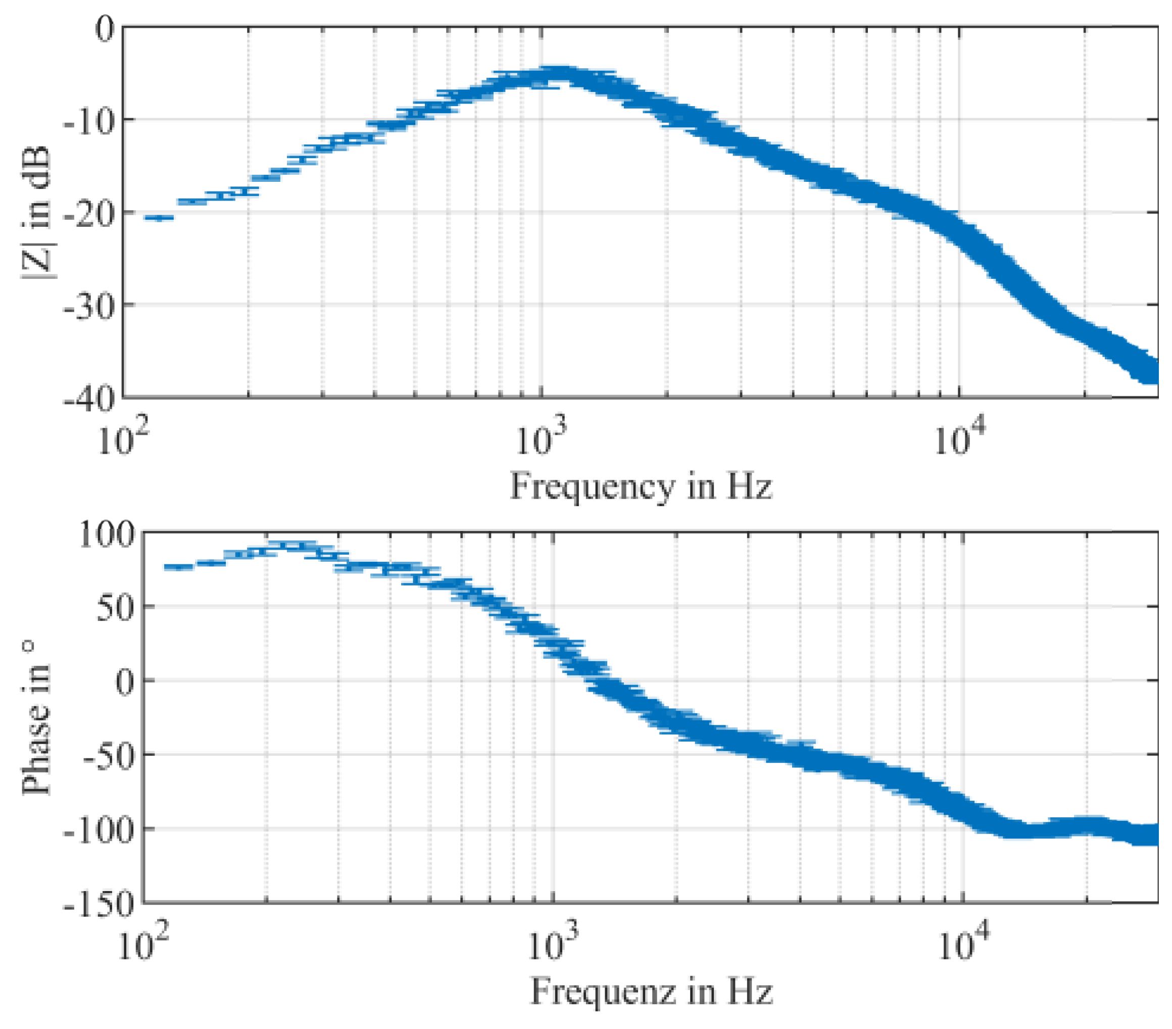
To further exemplify the validity of the wide bandwidth measurement, a set of 10 equal measurements with an i P R B S of 4 A were taken. Results with their standard deviation are given in Figure 23. As shown, the deviation between measurements is reasonably low, indicating high reproducibility. The results also show similar variance over a wide frequency range, with the exception of low frequencies. As expected from the simulation results, insufficient ADC triggering leads to wide bandwidth noise, visible in the whole frequency range.

6. Discussion on Measurement Procedure

When using external PRBS to measure a system, a few degrees of freedom can be selected which can affect measurement quality. While time discretization does not play a significant role in measurement quality for the converter investigated, we still advise to set f P R B S only as high as twice f N . Depending on whether digital or PWM sampling dominates, f P R B S can therefore be set to equal either f s or f s a m p . If the power converter’s internal structure is unknown, we advise determining the switching frequency by means of external measurement and assume f s a m p to be equal. If variable frequency topologies such as in [45,46,47,48,49] are used, f P R B S should be set close to the operating point frequency. With f P R B S set, Equation (38) can be used to determine the minimum excitation current. If the capacitance or value discretization are unknown, we advise a first measurement to judge the capacitance and assume an industry standard 12-bit ADC, adjusted for the maximum allowable voltage. The PRBS order O can be determined by the minimum frequency that is supposed to be measured, using Equation (27). This procedure should allow for accurate and fast impedance measurement using PRBS. If not, we suggest changing the excitation amplitude first, before changing f P R B S .

7. Conclusions

Output impedance measurement of power converters can be a powerful tool in DC grid stability estimation. Here, excitation with wide bandwidth signals can speed up measurement at little cost to measurement accuracy. As shown in this paper, clear criteria for accurate wide bandwidth measurements can be deduced from theoretical considerations. For parallel coupled current type PRBS signals, these criteria were verified in simulation as well as on a physical device under test. It is shown that especially the vertical resolution of the power converter’s digitalization can have a large impact on measurement. For the investigated type of converter and test signal type, horizontal resolution, i.e., sampling frequency, tends to only play a minor role relating to measurement. Further investigations of different types of signal coupling and their impact on aliasing as well as ADC excitation are still needed. Similarly, the investigations in this paper were limited to buck-type converters and might not be generalizable to any type of converter. While certain relations, like the capacitor–charge relation might still be applicable, especially aliasing might play a more pronounced role in different topologies. Additionally, means of softening the pulses, so as to only excite within a specified frequency range with less perturbation in the above Nyquist frequency band, might further enhance wide bandwidth excitation.

Author Contributions

Conceptualization, R.S.; Methodology, R.S., B.W. and M.M.; Software, R.S.; Validation, R.S. and M.B.; Formal analysis, R.S.; Investigation, R.S. and M.B.; Writing—original draft, R.S.; Writing—review & editing, M.B., B.W. and M.M.; Visualization, R.S.; Supervision, M.M. All authors have read and agreed to the published version of the manuscript.

Funding

This work was conducted within the project ECS4DRES. ECS4DRES is supported by the Chips Joint Undertaking under grant agreement number 101139790 and its members, including the top-up funding by Germany, Italy, Slovakia, Spain and The Netherlands. The APC was also funded by the FAU publication fund.

Data Availability Statement

The original contributions presented in this study are included in the article. Further inquiries can be directed to the corresponding author.

Conflicts of Interest

The authors declare on conflict of interest.

References

  1. Dragicevic, T.; Lu, X.; Vasquez, J.C.; Guerrero, J.M. DC Microgrids—Part II: A Review of Power Architectures, Applications, and Standardization Issues. IEEE Trans. Power Electron. 2016, 31, 3528–3549. [Google Scholar] [CrossRef]
  2. Boroyevich, D.; Cvetkovic, I.; Dong, D.; Burgos, R.; Wang, F.; Lee, F. Future electronic power distribution systems a contemplative view. In Proceedings of the 2010 12th International Conference on Optimization of Electrical and Electronic Equipment, Brasov, Romania, 20–22 May 2010; pp. 1369–1380. [Google Scholar]
  3. Hou, N.; Ding, L.; Gunawardena, P.; Wang, T.; Zhang, Y.; Li, Y.W. A Partial Power Processing Structure Embedding Renewable Energy Source and Energy Storage Element for Islanded DC Microgrid. IEEE Trans. Power Electron. 2023, 38, 4027–4039. [Google Scholar] [CrossRef]
  4. Santos, P.; Fonte, P.; Luis, R. Improvement of DC Microgrid Voltage Regulation Based on Bidirectional Intelligent Charging Systems. In Proceedings of the 2018 15th International Conference on the European Energy Market (EEM), Lodz, Poland, 27–29 June 2018; pp. 1–6. [Google Scholar]
  5. Schmidt, H.; Gutierrez, A.J.C.; Romani, A.; Crescentini, M.; Borger, K.; Chacon, R.; Forster, A.; Schwanninger, R.; Eberle, T.; März, M. The PROGRESSUS project—Highly efficient and trustworthy electronics, components and systems for the next generation energy supply infrastructure. In Proceedings of the 2023 AEIT International Conference on Electrical and Electronic Technologies for Automotive (AEIT AUTOMOTIVE), Modena, Italy, 17–19 July 2023; pp. 1–6. [Google Scholar]
  6. Schwanninger, R.; Friedrich, J.; Lavery, M.; Maerz, M. Investigation of a Decentralized Energy Management System for Undersupplied EV Charging Parks. In Proceedings of the 2024 IEEE Sixth International Conference on DC Microgrids (ICDCM), Columbia, SC, USA, 5–8 August 2024; pp. 1–7. [Google Scholar]
  7. Barth, M.; Gutwald, B.; Russwurm, E.; Lavery, M.; Schwanninger, R.; März, M.; Franke, J. Holistic Concept for Simulation-based Planning and Design of Hybrid AC/DC Energy Grids for Production Systems. SNE Simul. Notes Eur. 2024, 34, 61–70. [Google Scholar] [CrossRef]
  8. Schwanninger, R.; Schmitt, D.; Lavery, M.; Maerz, M. Output Impedance Measurement of Digitally Controlled Power Converters in LVDC-Grids. In Proceedings of the 2024 IEEE Sixth International Conference on DC Microgrids (ICDCM), Columbia, SC, USA, 5–8 August 2024. [Google Scholar]
  9. Enslin, J.; Heskes, P. Harmonic Interaction Between a Large Number of Distributed Power Inverters and the Distribution Network. IEEE Trans. Power Electron. 2004, 19, 1586–1593. [Google Scholar] [CrossRef]
  10. Dragicevic, T.; Lu, X.; Vasquez, J.C.; Guerrero, J.M. DC Microgrids—Part II: A Review of Power Architectures, Applications, and Standardization Issues. In Proceedings of the 2009 IEEE Electric Ship Technologies Symposium, Baltimore, MD, USA, 4 August 2009; pp. 428–432. [Google Scholar]
  11. Yang, X.; Pohlenz, S.; Schwanninger, R.; Schleippmann, N.; Wunder, B.; März, M. Modelling and Design of a Droop-Based Cascaded Controller for LLC Resonant Converter. In Proceedings of the 2023 IEEE Fifth International Conference on DC Microgrids (ICDCM), Auckland, New Zealand, 15–17 November 2023; pp. 1–6. [Google Scholar] [CrossRef]
  12. Lavery, M.; Schwanninger, R.; März, M. Use-Case-Dependent Modeling Approach for Computer Simulation of Hybrid AC-DC Grids. In Proceedings of the 2023 IEEE Fifth International Conference on DC Microgrids (ICDCM), Auckland, New Zealand, 15–17 November 2023; pp. 1–6. [Google Scholar]
  13. Ott, L.; Han, Y.; Wunder, B.; Maerz, M.; Bodensteiner, F. Evaluation of DC-DC-Converter Impedance Passivity Using Pseudo-Random Test Signals. In Proceedings of the 2018 International Exhibition and Conference for Power Electronics, Intelligent Motion, Renewable Energy and Energy Management (PCIM), Nuremberg, Germany, 5–7 June 2018. [Google Scholar]
  14. Zhang, X.; Ruan, X.; Zhong, Q.-C. Improving the Stability of Cascaded DC/DC Converter Systems via Shaping the Input Impedance of the Load Converter With a Parallel or Series Virtual Impedance. IEEE Trans. Ind. Electron. 2015, 62, 7499–7512. [Google Scholar] [CrossRef]
  15. Ye, Q.; Mo, R.; Shi, Y.; Li, H. A unified Impedance-based Stability Criterion (UIBSC) for paralleled grid-tied inverters using global minor loop gain (GMLG). In Proceedings of the 2015 IEEE Energy Conversion Congress and Exposition (ECCE), Montreal, QC, Canada, 20–24 September 2015; pp. 5816–5821. [Google Scholar]
  16. Hassan, R.; Wang, H.; Rehman, M.M.U.; Riar, B.; Zane, R. Nodal Impedance-Based Stability Analysis of Dc Nanogrids. In Proceedings of the 2018 IEEE 19th Workshop on Control and Modeling for Power Electronics (COMPEL), Padua, Italy, 25–28 June 2018. [Google Scholar]
  17. Schwanninger, R.; Roeder, G.; Wienzek, P.; Lavery, M.; Wunder, B.; Schellenberger, M.; Lorentz, V.; Maerz, M. Experimental Assessment of LVDC-Grid Stability Optimization using Circuit Simulation and Machine Learning. In Proceedings of the 2023 IEEE Fifth International Conference on DC Microgrids (ICDCM), Auckland, New Zealand, 15–17 November 2023; pp. 1–6. [Google Scholar]
  18. Bakhshizadeh, M.K.; Blaabjerg, F.; Hjerrild, J.; Kocewiak, L.; Bak, C.L. Improving the Impedance-Based Stability Criterion by Using the Vector Fitting Method. IEEE Trans. Energy Convers. 2018, 33, 1739–1747. [Google Scholar] [CrossRef]
  19. Riccobono, A.; Santi, E. A novel Passivity-Based Stability Criterion (PBSC) for switching converter DC distribution systems. In Proceedings of the 2012 Twenty-Seventh Annual IEEE Applied Power Electronics Conference and Exposition (APEC), Orlando, FL, USA, 5–9 February 2012; pp. 2560–2567. [Google Scholar] [CrossRef]
  20. Vesti, S.; Suntio, T.; Oliver, J.A.; Prieto, R.; Cobos, J.A. Impedance-Based Stability and Transient-Performance Assessment Applying Maximum Peak Criteria. IEEE Trans. Power Electron. 2013, 28, 2099–2104. [Google Scholar] [CrossRef]
  21. Zhang, C.; Molinas, M.; Rygg, A.; Cai, X. Impedance-Based Analysis of Interconnected Power Electronics Systems: Impedance Network Modeling and Comparative Studies of Stability Criteria. IEEE J. Emerg. Sel. Top. Power Electron. 2020, 8, 2520–2533. [Google Scholar] [CrossRef]
  22. Zhang, X.; Ruan, X.; Tse, C.K. Impedance-Based Local Stability Criterion for DC Distributed Power Systems. IEEE Trans. Circuits Syst. I Regul. Pap. 2015, 62, 916–925. [Google Scholar] [CrossRef]
  23. Middlebrook, R.D. Input filter considerations in design and application of switching regulators. Conf. Rec. IEEE IAS Annu. Meet. 1979, 11, 366–382. [Google Scholar]
  24. Miao, B.; Zane, R.; Maksimovic, D. A modified cross-correlation method for system identification of power converters with digital control. In Proceedings of the 2004 IEEE 35th Annual Power Electronics Specialists Conference (IEEE Cat. No.04CH37551), Aachen, Germany, 20–25 June 2004; pp. 3728–3733. [Google Scholar]
  25. Barkley, A.; Santi, E. Improved Online Identification of a DC–DC Converter and Its Control Loop Gain Using Cross-Correlation Methods. IEEE Trans. Power Electron. 2009, 24, 2021–2031. [Google Scholar] [CrossRef]
  26. Shirazi, M.; Morroni, J.; Dolgov, A.; Zane, R.; Maksimovic, D. Integration of Frequency Response Measurement Capabilities in Digital Controllers for DC–DC Converters. IEEE Trans. Power Electron. 2008, 23, 2524–2535. [Google Scholar] [CrossRef]
  27. Roinila, T.; Vilkko, M.; Taskinen, A. Improved fast frequency response measurements of switched-mode power supplies using Dirac-ideal PRBS excitation. In Proceedings of the 2009 2nd International Conference on Adaptive Science & Technology (ICAST), Accra, Ghana, 14–16 January 2009; pp. 175–181. [Google Scholar]
  28. Martin, D.; Santi, E.; Barkley, A. Wide bandwidth system identification of AC system impedances by applying pertubations to an existing converter. In Proceedings of the 2011 IEEE Energy Conversion Congress and Exposition, Phoenix, AZ, USA, 17–22 September 2011; pp. 2549–2556. [Google Scholar]
  29. Pan, P.; Hu, H.; He, Z.; Li, Y. Rapid Impedance Measurement Approach Based on Wideband Excitation for Single-Phase Four-Quadrant Converter of High-Speed Train. IEEE Trans. Instrum. Meas. 2021, 70, 9004611. [Google Scholar] [CrossRef]
  30. Roinila, T.; Abdollahi, H.; Arrua, S.; Santi, E. Online measurement of bus impedance of interconnected power electronics systems: Applying orthogonal sequences. In Proceedings of the 2017 IEEE Energy Conversion Congress and Exposition (ECCE), Cincinnati, OH, USA, 1–5 October 2017; pp. 5783–5788. [Google Scholar]
  31. Roinila, T.; Messo, T.; Luhtala, R.; Scharrenberg, R.; de Jong, E.C.W.; Fabian, A.; Sun, Y. Hardware-in-the-Loop Methods for Real-Time Frequency-Response Measurements of on-Board Power Distribution Systems. IEEE Trans. Ind. Electron. 2019, 66, 5769–5777. [Google Scholar] [CrossRef]
  32. Roinila, T.; Abdollahi, H.; Arrua, S.; Santi, E. Real-Time Stability Analysis and Control of Multiconverter Systems by Using MIMO-Identification Techniques. IEEE Trans. Power Electron. 2019, 34, 3948–3957. [Google Scholar] [CrossRef]
  33. Roinila, T.; Messo, T.; Santi, E. MIMO-Identification Techniques for Rapid Impedance-Based Stability Assessment of Three-Phase Systems in DQ Domain. IEEE Trans. Power Electron. 2018, 33, 4015–4022. [Google Scholar] [CrossRef]
  34. Berg, M.; Alenius, H.; Roinila, T. Rapid Multivariable Identification of Grid Impedance in DQ Domain Considering Impedance Coupling. IEEE J. Emerg. Sel. Top. Power Electron. 2022, 10, 2710–2721. [Google Scholar] [CrossRef]
  35. Mohammed, N.; Ciobotaru, M.; Town, G. Performance Evaluation of Wideband Binary Identification of Grid Impedance Using Grid-connected Inverters. In Proceedings of the 2019 21st European Conference on Power Electronics and Applications (EPE ‘19 ECCE Europe), Genova, Italy, 3–5 September 2019; pp. 1–10. [Google Scholar]
  36. Riccobono, A.; Mirz, M.; Monti, A. Noninvasive Online Parametric Identification of Three-Phase AC Power Impedances to Assess the Stability of Grid-Tied Power Electronic Inverters in LV Networks. IEEE J. Emerg. Sel. Top. Power Electron. 2018, 6, 629–647. [Google Scholar] [CrossRef]
  37. Mohammed, N.; Zhou, W.; Bahrani, B.; Hill, D.; Blaabjerg, F. PRBS-Based Impedance Measurement Tool for Stability Analysis of Black-Box EMT Models in PSCAD. In Proceedings of the 2024 4th International Conference on Emerging Smart Technologies and Applications (eSmarTA), Sana’a, Yemen, 6–7 August 2024; pp. 1–8. [Google Scholar]
  38. Sihvo, J.; Stroe, D.-I.; Messo, T.; Roinila, T. Fast Approach for Battery Impedance Identification Using Pseudo-Random Sequence Signals. IEEE Trans. Power Electron. 2020, 35, 2548–2557. [Google Scholar] [CrossRef]
  39. Roinila, T.; Messo, T. Online Grid-Impedance Measurement Using Ternary-Sequence Injection. IEEE Trans. Ind. Appl. 2018, 54, 5097–5103. [Google Scholar] [CrossRef]
  40. Basnet, H.; Tran, M.; Santi, E.; Roinila, T. Dynamical Characterization of STATCOM Application: Applying Computer-Optimized Orthogonal Perturbations. In Proceedings of the 2024 IEEE Sixth International Conference on DC Microgrids (ICDCM), Columbia, SC, USA, 8 August 2024. [Google Scholar]
  41. Sawma, J.; Khatounian, F.; Monmasson, E. A modified cross-correlation method for the identification of systems with large bandwidth. In Proceedings of the IECON 2012—38th Annual Conference on IEEE Industrial Electronics Society, Montreal, QC, Canada, 25–28 October 2012; pp. 2121–2126. [Google Scholar]
  42. Texas Instruments. TMS320F2837xD Dual-Core Real-Time Microcontrollers Datasheet (Rev. P); Texas Instruments: Dallas, TX, USA, 2024; pp. 109–110. [Google Scholar]
  43. LEM. Current Transducer LA 130-P datasheet (Version 5); LEM: Geneva, Switzerland, 2024; pp. 1–4. [Google Scholar]
  44. Analog Devices. LT1809/1810 Single/Dual 180 MHz, 350 V/µs Rail-to-Rail Input and Output Low Distortion Op Amps Datasheet (Rev. A); Analog Devices: Osaka, Japan, 2000; pp. 1–24. [Google Scholar]
  45. Al Attar,, H.; Hamida, M.A.; Ghanes, M.; Taleb, M. Review on Modeling and Control Strategies of DC–DC LLC Converters for Bidirectional Electric Vehicle Charger Applications. Energies 2023, 16, 3946. [Google Scholar] [CrossRef]
  46. Long, X.; Chen, D. Small Signal Modeling of LLC Converter with LED Load and Quasi-Resonant Controller Based Active Ripple Rejection. Energies 2023, 16, 3773. [Google Scholar] [CrossRef]
  47. Schwanninger, R.; Stöcklein, N.; Weitz, N.; Yang, X.; März, M. A Path to Configurable Solid State Transformers and Energy Routers: Introduction to Modular Active Cell Control. In IEEE Transactions on Power Electronics; IEEE: Piscataway, NJ, USA, 2025; pp. 1–18. [Google Scholar] [CrossRef]
  48. Marxgut, C.; Krismer, F.; Bortis, D.; Kolar, J.W. Ultraflat Interleaved Triangular Current Mode (TCM) Single-Phase PFC Rectifier. IEEE Trans. Power Electron. 2013, 29, 873–882. [Google Scholar] [CrossRef]
  49. Niu, P.; Guo, J.; Gao, Z.; Yan, J.; Gao, S. Research on Improved Technology of Totem-Pole Bridgeless PFC Circuit Based on Triangular Current Mode. Energies 2025, 18, 3886. [Google Scholar] [CrossRef]
Figure 1. Reconstructed signal y of a measured signal x with sufficient (a) and insufficient (b) excitation.
Energies 18 06121 g001
Figure 2. Simplified model of a 10 phase buck converter’s current control loop.
Energies 18 06121 g002
Figure 3. Simplified time variant model of the switching behavior of a half bridge with a triangular carrier. (a) shows the carrier and the PWM-Modulators input signal, (b) depicts the resulting PWM, and (c) gives the small signal reaction to the perturbation.
Energies 18 06121 g003
Figure 4. Effect of PWM on the open loop transfer function G O L and the feedback transfer function G O L , F B for two different frequency excitations d f 1 and d f 2 . The black arrow represents the origin axis at 0 Hz. (a) shows two sinusoidal perturbations (blue and green arrows) as well as the δ -comb representing the PWM (red arrows). The aliasing of the original perturbations are shown as dashed arrows in (b). In (c) these arrows are weighted with G O L . Due to aliasing, this affects G O L , F B as indicated in (d).
Energies 18 06121 g004
Figure 5. Simulation results and analytical models of a 10 phase buck converter’s current control loop.
Energies 18 06121 g005
Figure 6. Simplified time variant model of the switching behavior of a half bridge with a triangular carrier and digital sampling. (a) shows the carrier and the PWM-Modulators input signal, (b) depicts the resulting PWM, and (c) gives the small signal reaction to the perturbation.
Energies 18 06121 g006
Figure 7. Equivalent circuit of the PRBS-based impedance measurement system.
Energies 18 06121 g007
Figure 8. First 100 bits of a digital PRBS pattern (top) and measured currents with different amplitudes coupled into the grid (bottom) with 8 A (blue lines) and 4 A (red lines).
Energies 18 06121 g008
Figure 9. Spectrum of the i P R B S and v D U T measurements of a PRBS with f c , m i n , f P R B S , and f c , m a x indicated.
Energies 18 06121 g009
Figure 10. Three-dimensional model of the developed measurement system.
Energies 18 06121 g010
Figure 11. Equivalent circuit of the simulation used to verify the amplitude requirements for i P R B S . To simplify the simulation, a load converter is not included in the simulation.
Energies 18 06121 g011
Figure 12. Simulation results of the output current of a converter with and without voltage discretization (ideal) for different excitation amplitudes with f P R B S = 100 kHz. The results on the left are for a 200 µF with (a) at 1.25 A, (c) at 2.5 A and (e) at 5 A, the ones on the right are for a 400 µF output capacitance with (b) at 2.5 A, (d) at 5 A and (f) at 10 A.
Energies 18 06121 g012
Figure 13. Simulation results of the output current of a converter with and without voltage discretization (ideal) for different excitation amplitudes. The results on the left are for a 200 µF at 250 mΩ with (a) at 1.25 A, (c) at 2.5 A and (e) at 5 A, the ones on the right for a 400 µF output capacitance at 125 mΩ with (b) at 2.5 A, (d) at 5 A and (f) at 10 A.
Energies 18 06121 g013
Figure 14. Impact of a 400 kHz and a 100 kHz PRBS on an analog controlled converter with f N N of 100 kHz.
Energies 18 06121 g014
Figure 15. Impact of a 400 kHz PRBS on an analog controlled converter with f s of 100 kHz under different D 0 .
Energies 18 06121 g015
Figure 16. Impact of a 400 kHz and a 100 kHz PRBS on a digitally controlled converter with an f N d of 100 kHz.
Energies 18 06121 g016
Figure 17. Impact of a 400 kHz and a 100 kHz PRBS on a digitally controlled converter with an f N d of 25 kHz.
Energies 18 06121 g017
Figure 18. Impact of a 400 kHz and a 100 kHz PRBS on an analog controlled converter with an f s of 25 kHz.
Energies 18 06121 g018
Figure 19. Comparison of signal and noise amplitudes of the measurement.
Energies 18 06121 g019
Figure 20. Impact of the measurement system’s ADC resolution on the impedance measurement. The reduction to 12 bit has no impact on the measurement, with the red dots below the yellow dots (16 bit).
Energies 18 06121 g020
Figure 21. First 100 bits of an injected PRBS-shaped current used to measure the output impedance of a power converter.
Energies 18 06121 g021
Figure 22. Measurement results of the output impedance of a buck converter at different excitation currents.
Energies 18 06121 g022
Figure 23. Measurement results of a set of 10 measurements at 4 A. The standard deviation is given as error bars for each frequency.
Energies 18 06121 g023
Table 1. Components of the measurement system.
ComponentParameterValue
ADC [42]Sampling frequency 400 k H z
Resolution 16 b i t
Gain error 9 L S B
Offset error 9 L S B
SNR (at 10 kHz)90.2 dB
Current Sensor [43]Nominal current ± 130 A
Turns ratio ( N p / N s ) 1 : 1000
Linearity error < 0.1 %
Bandwidth (−1 dB)DC—150 kHz
Shunt ResistorResistance 100 m Ω
Tolerance ± 1 %
Temperature coefficient ± 100 p p m / K
Measurement Amplifiers [44]Unity gain bandwidth320 MHz
Slew rate 350 V / µ s
Common mode rejection ratio78 dB (@ 3 V)
Power supply rejection ratio87 dB
Input voltage range0 V–3 V
Input noise voltage density 16 n V / H z
Voltage BandpassFrequency range10 Hz–50 kHz
Passband attenuation 20 d B
Shunt Current BandpassFrequency range10 Hz–50 kHz
Passband attenuation 3.5 d B
Table 2. Simulation model parameters.
ParameterValue
MOSFET resistance 7.2 m Ω
Inductance 142 μ H
Inductor resistance 8 m Ω
Proportional current controller gain 10.87 1 k A
Integral current controller gain 23.85 1 k A · s
Input voltage 1 k V
Output voltage 500 V
Output capacitance 200 μ F | 400 μ F
Disclaimer/Publisher’s Note: The statements, opinions and data contained in all publications are solely those of the individual author(s) and contributor(s) and not of MDPI and/or the editor(s). MDPI and/or the editor(s) disclaim responsibility for any injury to people or property resulting from any ideas, methods, instructions or products referred to in the content.