Abstract
High-efficiency power management is essential for silicon photomultiplier (SiPM)-based sensing systems, especially in portable radiation detectors that demand long battery life and stable operation. Conventional fixed-frequency, voltage-mode boost converters face two critical issues: efficiency degradation at light load due to dominant switching losses, and narrow loop bandwidth in discontinuous conduction mode (DCM), which limits transient response. This work proposes a boost converter IC that integrates a pulse-skipped switching (PSS) scheme with a Gm-boosted compensator to address these challenges. The PSS method adaptively suppresses unnecessary switching events, significantly improving light-load efficiency, while the Gm-boosted compensator enhances loop gain, expanding the bandwidth and enabling faster recovery under dynamic conditions. Implemented in a 250 nm BCD process, the converter provides up to 30 V output from a 3.3–5 V supply with load currents up to 10 mA. Simulation results show a peak efficiency of 86.3% at 1 mA and a loop bandwidth increase of more than 14 times compared with a conventional fixed-frequency, voltage-mode design. Beyond radiation applications, the proposed converter is broadly applicable to battery-powered IoT, medical monitoring, and portable energy systems requiring efficient high-voltage generation.
1. Introduction
Silicon photomultipliers (SiPMs) have emerged as a key enabling technology in radiation detection, medical imaging, high-energy physics, and portable safety monitoring systems [1,2,3]. Compared with traditional photomultiplier tubes (PMTs), SiPMs offer compact size, mechanical robustness, and low-voltage operation, which make them particularly attractive for battery-powered instruments [4,5]. Despite these advantages, SiPMs still require relatively high bias voltages in the range of 25–30 V to ensure stable gain and low noise characteristics [6]. This creates a significant challenge for mobile sensing platforms that typically operate from low-voltage sources such as 3.3 V or 5 V batteries, where efficient step-up power conversion is essential for reliable long-term use. Figure 1 illustrates a typical SiPM-based mobile radiation detection system, where a compact boost converter must generate a stable 25–30 V bias from a limited battery supply. This highlights the critical role of power management ICs in ensuring both portability and measurement accuracy.
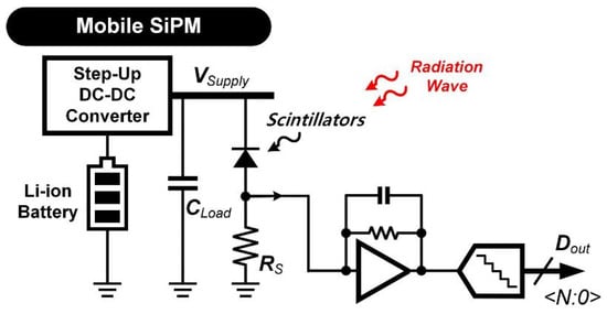
Figure 1.
SiPM-based mobile radiation detection system.
Conventional boost converters have been widely explored for high-voltage generation in sensor interfaces [7,8]. However, these designs face persistent limitations when applied to SiPM-based systems. First, efficiency degradation under light-load conditions becomes critical in conventional fixed-frequency, voltage-mode boost converters, particularly when operating in Discontinuous Conduction Mode (DCM), since radiation detectors often spend long periods in standby or low-current states [9]. In such cases, switching losses dominate and drastically reduce battery lifetime. Second, the loop bandwidth of conventional converters operating in DCM remains narrow, which slows down transient response and compromises output stability when the detected photon rate varies dynamically [10,11]. Additional challenges include increased circuit complexity and non-negligible power overhead in current-mode control implementations [12,13,14].
Addressing these challenges is not only relevant for nuclear and medical radiation detection but also for a broader class of photodiode-based sensing systems. Many chemical and biological sensors rely on photodiode or SiPM interfaces to detect fluorescence, luminescence, or scintillation signals [15,16,17]. These applications likewise demand stable high-voltage biasing with low power consumption and fast recovery, especially in portable and long-duration monitoring scenarios. Therefore, improving the efficiency and loop stability of boost converter circuits has direct implications for radiation dosimetry platforms.
In this work, we propose a boost converter IC that integrates pulse-skipped switching (PSS) to suppress unnecessary switching activity under light-load conditions [18] and a Gm-boosted compensator to extend loop bandwidth [19,20]. Simulation results in a 250 nm BCD process demonstrate improved efficiency, a bandwidth increase of over 14 times, and robust regulation even under process variation and radiation-induced charge injection. The remainder of this paper is organized as follows. Section 2 reviews conventional high-voltage boost converters and their limitations. Section 3 presents the proposed architecture and design methodology. Section 4 provides simulation results. Section 5 discusses advantages, limitations, and potential future directions. Finally, Section 6 concludes this work with implications for broader applicable systems.
2. Prior Arts
2.1. Boost Converters with Embedded Readout
One representative approach to simplify SiPM-based detection systems is the integration of readout circuits directly within the boost converter IC [21]. By combining the high-voltage generation stage with charge-sensitive amplification or signal conditioning, the overall system complexity can be reduced, resulting in a more compact and portable solution. Such integration also minimizes parasitic effects between separate power and readout blocks, thereby improving signal fidelity. Figure 2 illustrates a typical architecture where the SiPM readout is embedded in the boost converter.
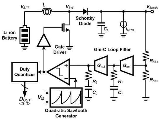
Figure 2.
Conventional boost converter IC with embedded readout circuits.
However, these designs exhibit noticeable efficiency degradation in deep light-load conditions, typically below 1 mA, which are common in low-count-rate radiation environments [22]. The primary drawback stems from switching losses at the high-voltage node, where large parasitic capacitance and inductance result in significant energy dissipation during each cycle. This issue is particularly pronounced for portable detectors operating in standby or monitoring modes, where switching losses dominate overall power consumption.
2.2. Current-Mode Control for Improved Loop Bandwidth
Another widely investigated method is the application of current-mode control to high-voltage boost converters [23]. By directly regulating the inductor current, this approach reduces output voltage ripple and enhances loop stability. In principle, current-mode control provides a wider bandwidth compared with conventional voltage-mode counterparts, which is advantageous for transient response and stability. A typical current-mode controlled boost converter structure is shown in Figure 3.
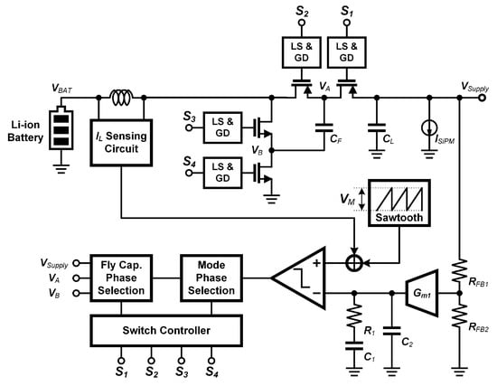
Figure 3.
Conventional boost converter IC with current mode control.
Nevertheless, when applied to high-voltage and light-load SiPM systems, several limitations arise. Current sensing incurs non-negligible power overhead, which reduces overall efficiency in ultra-low-current operation [24]. Additionally, implementing accurate current sensing requires additional circuits for voltage scaling and offset cancellation, increasing area and design complexity [25]. Layout constraints introduced by sensing elements further complicate optimization of the power stage, limiting achievable efficiency.
2.3. Other Recent Approaches
Beyond these conventional categories, several works have explored alternative methods such as adaptive mode switching [26], resonant topologies [27], or digitally assisted compensation techniques [28]. Adaptive mode switching can reduce switching losses by dynamically transitioning between DCM and pulse-frequency modulation (PFM). Resonant or quasi-resonant boost converters achieve soft switching, thereby improving light-load efficiency at the expense of increased design complexity. Digitally assisted loops, on the other hand, enhance transient response but require additional circuitry and may consume significant quiescent power. While these methods provide valuable improvements, they are often less suited for highly constrained portable systems due to overhead in power, area, or control logic (Table 1).

Table 1.
Summary table.
3. Proposed Boost Converter IC
The proposed boost converter IC is designed to address the dual challenges of light-load efficiency degradation and limited loop bandwidth in SiPM-based radiation and chemosensor systems. The overall architecture is illustrated in Figure 4, which presents the block diagram of the converter along with the key control concept. The design follows a conventional boost topology, composed of an off-chip inductor, an integrated high-voltage MOSFET switch, a diode-connected rectifier, and an output capacitor that generates the required bias voltage. On the control side, the architecture incorporates an error amplifier, a pulse-skipped switching (PSS) controller, and a Gm-boosted compensator.
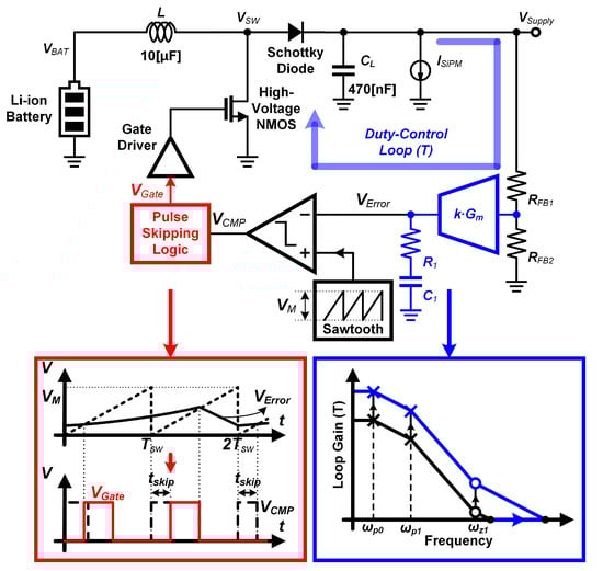
Figure 4.
Proposed boost converter IC architecture.
The error amplifier continuously monitors the output voltage through a feedback network and compares it with a reference. Its output serves as the control signal that reflects the deviation of the output from the target bias. This signal is processed by the PSS controller, which determines whether a switching cycle is required. During heavy load or transient conditions, the PSS controller enables continuous switching to quickly supply charge to the output. However, at light load, the controller intentionally skips cycles once the error signal falls below a defined threshold, thereby reducing the effective switching frequency and suppressing unnecessary switching losses.
In parallel, the Gm-boosted compensator stabilizes the feedback loop and enhances the dynamic performance of the system. By embedding an auxiliary transconductance boosting loop within the folded-cascode OTA, the compensator increases the effective loop gain without adding significant complexity. This ensures that the converter achieves wide bandwidth and fast transient recovery, overcoming the inherent limitations of discontinuous conduction mode (DCM).
Overall, Figure 4 highlights how the proposed boost converter combines conventional power conversion elements with novel control techniques. The block diagram underscores the dual contribution of PSS for efficiency and Gm-boosted compensation for loop bandwidth, providing a clear conceptual overview before detailed analysis in the following subsections.
3.1. Pulse-Skipped Switching Logic and Operation
A key innovation of the proposed design is the integration of a pulse-skipped switching (PSS) mechanism that adaptively reduces switching losses at light load. Figure 5 illustrates both the logic configuration of the PSS controller and its representative operating waveforms. The logic is implemented using a digital pulse-width modulation (PWM) generator with an embedded shift register. The error amplifier output is compared against a predefined threshold, and the resulting digital control word determines the number of active switching cycles permitted within a given time window.
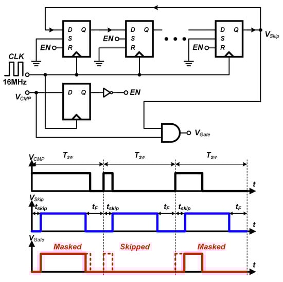
Figure 5.
Proposed pulse-skipped switching circuits and operation principle.
The use of a shift-register-based digital PWM structure provides two advantages. First, it allows precise adjustment of the skipping ratio (e.g., skipping every second or third pulse) according to the magnitude of the error voltage. This fine-grained control ensures that the converter can maintain stable regulation even under sub-milliampere loads. Second, the digital implementation offers robustness against process and temperature variations, which can otherwise introduce nonlinearity in analog control schemes.
The accompanying waveform in Figure 5 demonstrates how switching cycles are suppressed when the error voltage is small. During heavy load or transient conditions, the PSS controller enables continuous switching to maintain fast response. At light load, however, the controller gates off consecutive switching cycles, effectively lowering the switching frequency. Larger charge packets are delivered during the active cycles, so that the average output remains constant while the total switching loss is reduced. Simulation confirms that this adaptive strategy yields significant efficiency improvements at light load without introducing excessive output ripple.
3.2. Gm-Boosted Compensator
To overcome the limited loop bandwidth inherent in discontinuous conduction mode (DCM), the proposed design employs a Gm-boosted compensation technique, as depicted in Figure 6. The compensator is based on a folded cascode OTA, which is a common choice in Gm-C feedback networks due to its high output impedance and stable operation. However, a conventional OTA provides limited transconductance, which constrains the loop gain and bandwidth of the system.
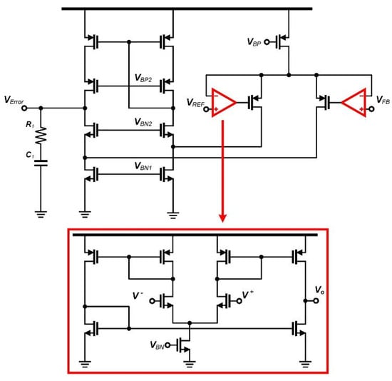
Figure 6.
Proposed Gm-boosted compensator.
In the proposed structure, a current-mirror OTA is embedded into the input stage of the folded cascode amplifier. This additional feedback loop reduces the effective source impedance of the input transistors, thereby increasing their transconductance without altering the high output impedance at the OTA’s drain node. As a result, the overall effective transconductance can be expressed as:
where Aboost is the gain and ωp, ωz is the pole and zero introduced by the auxiliary current mirror OTA.
This architecture provides a dual benefit. First, the loop gain is increased, which shifts the crossover frequency to higher values and expands the control bandwidth. In simulation, the loop bandwidth improved more than 14 times, reaching approximately 125 kHz. Second, because the boosting path primarily modifies the small-signal impedance of the input transistors, the high output impedance of the folded-cascode stage is preserved, ensuring that stability is not compromised. Importantly, the additional circuitry consumes negligible power compared with the overall bias currents of the OTA, making this approach highly efficient.
4. Performance Validation
This section presents performance validation of the proposed boost converter IC, obtained through detailed circuit-level simulations using a 250 nm BCD process model. The results confirm the effectiveness of the proposed architecture in improving light-load efficiency, extending loop bandwidth, and ensuring stable operation under radiation-induced disturbances. The IC layout design was performed using the Cadence Virtuoso® platform, and all circuit simulations were conducted with the Spectre® Circuit Simulator.
4.1. Transient Response with Pulse-Skipped Switching
Figure 7 compares the transient response of a conventional fixed-frequency boost converter with that of the proposed pulse-skipped switching (PSS) scheme under ultra-light-load conditions (<1 mA). In the conventional design, the switching node continues to toggle every cycle, leading to unnecessary energy dissipation and slow recovery of the output voltage. In contrast, the PSS approach selectively skips switching cycles once the error amplifier output indicates that the bias is well regulated. As shown in the waveform, the proposed method reduces switching events by two-thirds while maintaining stable output regulation. This translates into a reduction of switching loss by approximately 66%, leading to markedly higher efficiency in standby or low-count-rate scenarios where light-load operation dominates.
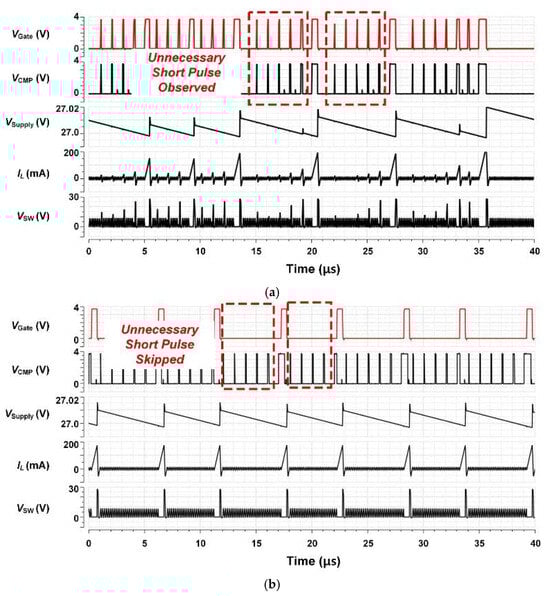
Figure 7.
Transient response comparison between (a) a conventional fixed-frequency boost converter and (b) the proposed pulse-skipped switching scheme under ultra-light-load operation (<1 mA).
4.2. Loop Behavior with Gm-Boosted Compensation
The small-signal control loop behavior with and without the proposed Gm-boosted compensator is shown in Figure 8. Without compensation, the loop bandwidth is constrained by the low-frequency pole of the DCM power stage, resulting in slow transient response and limited stability margin. Incorporating the Gm-boosted structure increases the effective transconductance of the error amplifier, thereby shifting the crossover frequency more than 14 times higher, to approximately 125 kHz. The Bode plot demonstrates that the gain margin and phase margin remain sufficient, confirming that stability is preserved while transient recovery is significantly accelerated. This improvement is essential for maintaining reliable bias conditions when SiPM or photodiode currents vary dynamically.
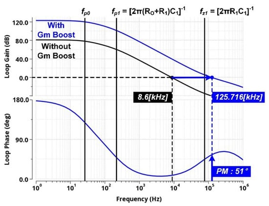
Figure 8.
Small-signal loop behavior of the proposed boost converter with and without Gm-boosted compensation, showing bandwidth extension by more than 14 times.
Furthermore, to verify the robustness of the control loop against process variations, extensive corner simulations were conducted. As shown in Figure 9, the loop gain and phase were evaluated across five process corners. The results demonstrate that the converter maintains stable operation across all conditions. The phase margin remains above 48.5° even in the worst-case (FF) corner, ensuring loop stability. The crossover frequency varies from approximately 103 kHz to 150 kHz, confirming that the wide bandwidth is consistently achieved. This analysis confirms that the proposed design is robust and insensitive to manufacturing process variations.
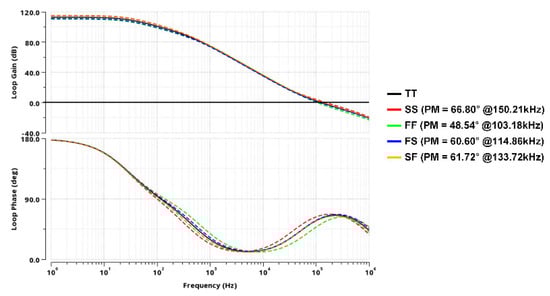
Figure 9.
Small-signal loop behavior across process corners (TT, SS, FF, FS, SF), demonstrating robust stability and bandwidth.
4.3. Radiation-Induced Charge Injection Response
To evaluate the converter under practical operating conditions, a radiation-induced charge injection model was applied. As illustrated in Figure 10, a transient 10 mA current pulse with 200 ns duration was periodically introduced at the output to emulate photon-induced charge bursts. In the conventional boost converter, such perturbations often lead to large voltage deviations and prolonged recovery. In contrast, the proposed design quickly absorbs the injected charge and restores the output within microseconds, with minimal ripple. This stable biasing ensures accurate photon counting in SiPM detectors and prevents distortion of sensor outputs in chemosensor applications.
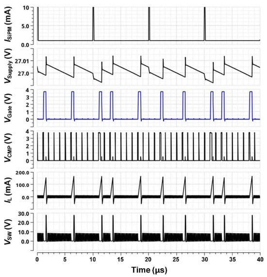
Figure 10.
Output voltage transient response under radiation-induced charge injection (10 mA, 200 ns pulse), demonstrating stable bias recovery with the proposed boost converter.
5. Discussion
The proposed boost converter demonstrates significant improvements over conventional designs, particularly in applications where SiPMs or photodiode-based chemosensors require a stable high-voltage bias under light-load conditions. The adoption of pulse-skipped switching (PSS) and Gm-boosted compensation allows the converter to achieve both high efficiency and wide loop bandwidth, which are typically conflicting objectives in discontinuous conduction mode (DCM) converters.
Figure 11 shows the layout of the proposed boost converter IC implemented in a 250 nm BCD process. The active area measures approximately 0.96 × 0.58 mm2, which highlights the compactness of the design while accommodating high-voltage devices. The integration of the control circuits, including the PSS controller and the Gm-boosted OTA, demonstrates the feasibility of implementing advanced compensation and switching schemes within a limited chip area suitable for portable sensing platforms.
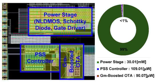
Figure 11.
Layout of the proposed boost converter IC implemented in a 250 nm BCD process and chart of power consumption of each block.
A quantitative comparison with prior works is summarized in Table 2. As shown, the proposed design achieves an efficiency of 86.3% at 1 mA load, which is more than 10% higher than several conventional approaches operating under similar conditions. In addition, the loop bandwidth reaches approximately 125 kHz, representing a more than 14 times improvement compared with conventional DCM converters. These results position the proposed architecture favorably against both voltage-mode and current-mode controlled boost converters, especially for ultra-light-load applications. The power efficiency was calculated from the steady-state transient simulation results using the following formula:
Here, is the average output power delivered to the load, and is the average input power drawn from the battery (). The simulation accounts for all major power loss mechanisms, including conduction losses in the power NMOS and Schottky diode, switching losses at the node, and the quiescent power consumption of the internal control circuitry (e.g., Gm-boosted compensator, PSS logic, and gate driver).
Table 2.
Performance comparison of the proposed boost converter with representative prior works.
Despite these advantages, some limitations should be acknowledged. First, while the PSS scheme effectively suppresses switching losses, it may introduce additional spectral components in the switching waveform, which could lead to increased EMI under certain conditions. Second, although the Gm-boosted compensation increases bandwidth with minimal power overhead, the additional current paths still contribute to a small increase in quiescent consumption. Finally, the reliance on DCM operation inherently limits the achievable output ripple suppression compared with continuous conduction mode (CCM) designs.
Looking ahead, several directions may further enhance the proposed design. Resonant or quasi-resonant converter topologies may provide an alternative approach for light-load high-voltage generation, reducing EMI while maintaining efficiency. Digital-assisted compensation techniques may also be employed to dynamically adjust loop parameters, improving robustness across wide operating conditions. These extensions, along with further robustness analyses such as Monte Carlo and corner simulations, will be explored in future work to strengthen the applicability of the proposed architecture to both radiation detection and broader chemosensor systems.
6. Conclusions
In this work, a high-efficiency boost converter IC has been presented for SiPM and photodiode-based sensing applications, extended from [29]. The proposed architecture integrates a pulse-skipped switching (PSS) scheme and a Gm-boosted compensator to simultaneously improve light-load efficiency and loop bandwidth, two conflicting challenges in discontinuous conduction mode (DCM) operation. Implemented in a 250 nm BCD process, the converter achieves a stable output voltage up to 30 V from a 3.3–5 V supply, with peak efficiency of 86.3% at 1 mA load and a loop bandwidth improvement exceeding 14 times compared with conventional designs.
The simulation results confirm that the PSS technique effectively reduces switching losses under ultra-light-load conditions, while the Gm-boosted compensation expands the control bandwidth without incurring significant power overhead. These improvements enable the converter to provide robust bias stability, even under dynamic conditions such as radiation-induced charge injection.
Beyond radiation detection, the proposed design has broader implications for portable IoT devices, biomedical monitors, renewable-energy-powered sensing platforms, and battery-limited systems, where long-term stability, high efficiency, and compact integration are critical. By addressing fundamental limitations of existing boost converter designs, this work contributes a practical and versatile power management solution. Future research will focus on exploring resonant topologies and digitally assisted compensation techniques to further enhance performance and robustness across diverse sensing environments.
Author Contributions
Conceptualization, H.J.; writing—original draft preparation, W.K.; writing—review and editing, S.-U.S.; visualization, H.N.; supervision, H.J.; project administration, H.J. All authors have read and agreed to the published version of the manuscript.
Funding
This work was supported by the Technology Innovation Program (RS-2024-00404313, Development of a 650 V GaN-based power converter single IC for mobile device charging adapter) funded By the Ministry of Trade, Industry & Energy (MOTIE, Korea) and this research was supported by National R&D Program through the National Research Foundation of Korea(NRF) funded by Ministry of Science and ICT (No. RS-2020-NR047143).
Data Availability Statement
The original contributions presented in this study are included in the article. Further inquiries can be directed to the corresponding authors.
Acknowledgments
The EDA tool was supported by the IC Design Education Center (IDEC), Republic of Korea.
Conflicts of Interest
The authors declare no conflicts of interest.
References
- Hu, Q.; Ye, H.; Jin, G. A SiPM-Based Wireless Neutron-Gamma Spectrometer for Remote Monitoring. In Proceedings of the 2023 6th International Conference on Electronics Technology (ICET), Chengdu, China, 26–29 May 2023; pp. 955–959. [Google Scholar] [CrossRef]
- Atanov, N.; Baranov, V.; Budagov, J.; Davydov, Y.I.; Glagolev, V.; Tereshchenko, V.; Usubov, Z.; Cervelli, F.; Di Falco, S.; Donati, S.; et al. Design and Status of the Mu2e Crystal Calorimeter. IEEE Trans. Nucl. Sci. 2018, 65, 2073–2080. [Google Scholar] [CrossRef]
- Mackewn, J.E.; Lerche, C.W.; Weissler, B.; Sunassee, K.; de Rosales, R.T.M.; Phinikaridou, A.; Salomon, A.; Ayres, R.; Tsoumpas, C.; Soultanidis, G.M.; et al. PET Performance Evaluation of a Pre-Clinical SiPM-Based MR-Compatible PET Scanner. IEEE Trans. Nucl. Sci. 2015, 62, 784–790. [Google Scholar] [CrossRef]
- Garutti, E. Silicon photomultipliers for high energy physics detectors. In Proceedings of the Workshop on Fast Cherenkov Detectors-Photon Detection, Dirac Design and DAQ, Giessen, Germany, 4–6 April 2011. [Google Scholar]
- Ruch, M.L.; Sivels, C.B.; Czyz, S.A.; Flaska, M.; Pozzi, S.A. Comparison between silicon photomultipliers and photomultiplier tubes for pulse shape discrimination with stilbene. In Proceedings of the 2014 IEEE Nuclear Science Symposium and Medical Imaging Conference (NSS/MIC), Seattle, WA, USA, 8–15 November 2014; pp. 1–3. [Google Scholar] [CrossRef]
- Carimatto, A.; Mandai, S.; Venialgo, E.; Gong, T.; Borghi, G.; Schaart, D.R.; Charbon, E. 11.4 A 67,392-SPAD PVTB-compensated multi-channel digital SiPM with 432 column-parallel 48ps 17b TDCs for endoscopic time-of-flight PET. In Proceedings of the 2015 IEEE International Solid-State Circuits Conference—(ISSCC) Digest of Technical Papers, San Francisco, CA, USA, 22–26 February 2015; pp. 1–3. [Google Scholar] [CrossRef]
- Santoro, D.; Gallice, N.; Bassani, M.; Cova, P.; Delmonte, N.; Lazzaroni, M.; Trabattoni, V.; Zani, A. DC-DC Boost Converter Design with Analog Feedback Control for Cryogenic Applications. IEEE Access 2025, 13, 23220–23233. [Google Scholar] [CrossRef]
- Maxim Integrated. MAX618 28V Internal Switch, Step-Up DC-DC Converter Datasheet. Available online: https://www.analog.com/en/products/max618.html (accessed on 25 August 2025).
- Reverter, F.; Gasulla, M. Optimal Inductor Current in Boost DC/DC Converters Operating in Burst Mode Under Light-Load Conditions. IEEE Trans. Power Electron. 2016, 31, 15–20. [Google Scholar] [CrossRef]
- Sun, J.; Mitchell, D.M.; Greuel, M.F.; Krein, P.T.; Bass, R.M. Averaged modeling of PWM converters operating in discontinuous conduction mode. IEEE Trans. Power Electron. 2001, 16, 482–492. [Google Scholar] [CrossRef]
- Hwang, Y.-S.; Shih, R.-L.; Fu, P.-H.; Hsiao, Y.-J.; Chen, J.-J.; Yu, C.-C. A compact fast-transient charge-pump boost converter using hysteretic compensated techniques. In Proceedings of the 2016 IEEE International Conference on Electron Devices and Solid-State Circuits (EDSSC), Hong Kong, China, 3–5 August 2016; pp. 484–487. [Google Scholar] [CrossRef]
- Ying, Y.; Chen, S.; Lee, J.; Ge, T. A 95% efficiency Buck-Boost Converter with Full-Cycle Continuous Current Sensing and Adaptive Mode Control. In Proceedings of the 2025 IEEE International Symposium on Circuits and Systems (ISCAS), London, UK, 25–28 May 2025; pp. 1–5. [Google Scholar] [CrossRef]
- Zhu, L.; Chen, B.; Zheng, Y.; Guo, J.; Ho, M.; Leung, K.N.; Chen, D.; Liu, Y. A fast-response buck-boost DC-DC converter with constructed full-wave current sensor. In Proceedings of the 2016 International Symposium on Integrated Circuits (ISIC), Singapore, 12–14 December 2016; pp. 1–4. [Google Scholar] [CrossRef]
- Biswas, K.; Ray, O. Calibration Method of Equivalent Series Resistance Parameter for Nonintrusive Current Sensors Used in DC–DC Power Electronic Converters. IEEE Sens. Lett. 2022, 6, 6002904. [Google Scholar] [CrossRef]
- Dhawangale, A.; Bharadwaj, R.; Mukherji, S.; Kundu, T. UV photodiode based portable fiber optic biosensor. In Proceedings of the 2010 International Conference on Systems in Medicine and Biology, Kharagpur, India, 16–18 December 2010; pp. 335–338. [Google Scholar] [CrossRef]
- He, C.; Chen, C.; Wang, K. Non-Line-of-Sight Indoor Optical Wireless Communication Using a Silicon Photomultiplier (SiPM). In Proceedings of the 2025 30th OptoElectronics and Communications Conference (OECC) and 2025 International Conference on Photonics in Switching and Computing (PSC), Sapporo, Japan, 29 June–3 July 2025; pp. 1–4. [Google Scholar] [CrossRef]
- Gounella, R.; Ferreira, G.M.; Amorim, M.L.M.; Soares, J.N., Jr.; Carmo, J.P. A Review of Optical Sensors in CMOS. Electronics 2024, 13, 691. [Google Scholar] [CrossRef]
- Kapat, S.; Mandi, B.C.; Patra, A. Voltage-Mode Digital Pulse Skipping Control of a DC–DC Converter with Stable Periodic Behavior and Improved Light-Load Efficiency. IEEE Trans. Power Electron. 2016, 31, 3372–3379. [Google Scholar] [CrossRef]
- Bult, K.; Geelen, G.J.G.M. A fast-settling CMOS op amp for SC circuits with 90-dB DC gain. IEEE J. Solid-State Circuits 1990, 25, 1379–1384. [Google Scholar] [CrossRef]
- Li, S.; Yulin, Q. Design of a Fully Differential Gain-Boosted Folded-Cascode Op Amp with Settling Performance Optimization. In Proceedings of the 2005 IEEE Conference on Electron Devices and Solid-State Circuits, Hong Kong, China, 19–21 December 2005; pp. 441–444. [Google Scholar] [CrossRef]
- Jeon, H.; Shin, S.-U. A Power/Hardware-Efficient SiPM Readout IC Embedded in a Boost Converter for Mobile Radiation Dosimeters. IEEE Trans. Power Electron. 2023, 38, 657–665. [Google Scholar] [CrossRef]
- Park, Y.-J.; Park, J.-H.; Kim, H.-J.; Ryu, H.; Kim, S.; Pu, Y.; Hwang, K.C.; Yang, Y.; Lee, M.; Lee, K.-Y. A Design of a 92.4% Efficiency Triple Mode Control DC–DC Buck Converter with Low Power Retention Mode and Adaptive Zero Current Detector for IoT/Wearable Applications. IEEE Trans. Power Electron. 2017, 32, 6946–6960. [Google Scholar] [CrossRef]
- Lee, S.-J.; Jeong, Y.-W.; Shin, S.-U. A Three-Level Boost Converter with Fully State-Based Phase Selection Technique for High-Speed VCF Calibration and Smooth Mode Transition. IEEE J. Solid-State Circuits 2023, 58, 3544–3554. [Google Scholar] [CrossRef]
- Patel, A.M.; Ferdowsi, M. Advanced Current Sensing Techniques for Power Electronic Converters. In Proceedings of the 2007 IEEE Vehicle Power and Propulsion Conference, Arlington, TX, USA, 9–12 September 2007; pp. 524–530. [Google Scholar] [CrossRef]
- Huang, W.; Yang, X.; Ling, C. A novel current sensing circuit for Boost DC-DC converter. In Proceedings of the 2012 IEEE International Conference on Anti-Counterfeiting, Security, and Identification, Taipei, Taiwan, 24–27 August 2012; pp. 1–4. [Google Scholar] [CrossRef]
- Shin, Y.-H.; Kim, H.-Y.; Kim, J.-W.; Choi, S.-Y.; Kim, Y.-S.; Choi, H.-Y. Efficiency improvement of dual mode DC-DC buck converter under light load using PTWS with a zero current detector. In Proceedings of the 2017 International Conference on Circuits, System and Simulation (ICCSS), London, UK, 14–17 July 2017; pp. 72–75. [Google Scholar] [CrossRef]
- Alaql, F.; Batarseh, I. Review and Comparison of Resonant DC-DC Converters for Wide-Output Voltage Range Applications. In Proceedings of the 2020 IEEE Energy Conversion Congress and Exposition (ECCE), Detroit, MI, USA, 11–15 October 2020; pp. 1197–1203. [Google Scholar] [CrossRef]
- Singh, M.; Fayed, A.A. A 1-A 6-MHz Digitally Assisted Buck–Boost Converter with Seamless Mode Transitions and Fast Dynamic Performance for Mobile Devices. IEEE Trans. Power Electron. 2021, 36, 4338–4351. [Google Scholar] [CrossRef]
- Kim, W.; Noh, H.; Jeon, H. A High-Efficient, Wide Loop BW Boost Converter IC with Pulse Skipped Switching and Gm-Boosted Compensator for Light-Load SiPM. In Proceedings of the 2025 IEEE 68th International Midwest Symposium on Circuits and Systems (MWSCAS), Lansing, MI, USA, 10–13 August 2025; pp. 1054–1058. [Google Scholar]


Disclaimer/Publisher’s Note: The statements, opinions and data contained in all publications are solely those of the individual author(s) and contributor(s) and not of MDPI and/or the editor(s). MDPI and/or the editor(s) disclaim responsibility for any injury to people or property resulting from any ideas, methods, instructions or products referred to in the content. |
© 2025 by the authors. Licensee MDPI, Basel, Switzerland. This article is an open access article distributed under the terms and conditions of the Creative Commons Attribution (CC BY) license (https://creativecommons.org/licenses/by/4.0/).