Article

Design and Demonstration of a 10 kV, 60 A SiC MOSFET-Based Medium-Voltage Power Module

by
Kai Xiao
1,
Yining Zhang
1,
Shuming Tan
1,
Jianyu Pan
2,
Hao Feng
2,
Yuxi Liang
2 and
Zheng Zeng
2,*
1
CSG EHV Electric Power, Research Institute, China Southern Power Grid Company Limited, Guangzhou 510663, China
2
State Key Laboratory of Power Transmission Equipment Technology, Chongqing University, Chongqing 400044, China
*
Author to whom correspondence should be addressed.
Energies 2025, 18(16), 4407; https://doi.org/10.3390/en18164407
Submission received: 27 June 2025 / Revised: 3 August 2025 / Accepted: 8 August 2025 / Published: 19 August 2025

Abstract

Silicon carbide (SiC) MOSFETs with voltage ratings above 3.3 kV are emerging as key enablers for next-generation medium-voltage (MV) power conversion systems, offering superior blocking capabilities, faster switching speeds, and an improved thermal performance compared to conventional silicon IGBTs. However, the practical deployment of 10 kV SiC devices remains constrained by the immaturity of high-voltage chip and packaging technologies. Current development is often limited to engineering samples provided by a few suppliers and custom packaging solutions evaluated only in laboratory settings. To advance the commercialization of 10 kV SiC power modules, this paper presents the design and characterization of a 10 kV, 60 A half-bridge module employing the XHP housing and newly developed SiC MOSFET chips from China Electronics Technology Group Corporation (CETC). Electro-thermal simulations based on a finite element analysis were conducted to extract key performance parameters, with a measured parasitic inductance of 24 nH and a thermal resistance of 0.0948 K/W. To further validate the packaging concept, a double-pulse test platform was implemented. The dynamic switching behavior of the module was experimentally verified under a 6 kV DC-link voltage, demonstrating the feasibility competitiveness of this approach and paving the way for the industrial adoption of 10 kV SiC technology in MV applications.

1. Introduction

Medium-voltage (MV) SiC MOSFETs—particularly those with blocking voltages above 3.3 kV—have emerged as promising candidates for next-generation power conversion systems [1,2,3]. Compared to conventional Si IGBTs, they offer a higher blocking capability, faster switching speed, and superior thermal performance. These advantages enable simplified converter topologies, reduced device counts, and lower switching losses, ultimately leading to enhanced reliability, improved efficiency, and increased power density in MV applications [4,5,6,7,8]. However, SiC MOSFETs with blocking voltages above 3.3 kV are still in the engineering sample stage and have not yet been adopted in commercial applications, primarily due to the immaturity of the high-voltage chip and packaging technologies. In terms of chips, CREE introduced the first 10 kV, 123 mΩ·cm2 4H-SiC power DMOSFET in 2004 [9]. Since then, multiple iterations of the 10 kV SiC chip have been developed, with the current rating of a single chip increasing from 5 A to 20 A [10,11,12,13]. In terms of power modules, numerous research institutions have developed custom-designed packages based on CREE’s 10 kV SiC MOSFET chips and have carried out a detailed characterization of the designed power modules. In 2016, CREE released a 240 A half-bridge power module based on its third-generation 10 kV SiC chips, with 18 chips paralleled per switch. This remains the highest current-rated 10 kV SiC power module reported to date [14]. Furthermore, a comprehensive characterization of the module was carried out [15]. Regarding packaging design, high-current applications are typically accompanied by large di/dt, which induce severe voltage overshoots and oscillations across the chips. To mitigate these effects, advanced substrate layouts and packaging architectures are employed to minimize parasitic inductance and ensure balanced current sharing [16,17,18]. In MV systems operating at 10 kV, transient dv/dt as high as 250 kV/μs have been observed—nearly two orders of magnitude greater than those typically seen in silicon IGBTs. To suppress parasitic capacitive coupling without compromising switching speed, strategies such as geometric optimization, the use of low-permittivity dielectrics, and the introduction of high-impedance paths for common-mode currents have been widely adopted [19,20,21,22]. At present, research on the packaging of 10 kV SiC chips is largely limited to custom designs developed in laboratory settings [23]. These efforts have predominantly focused on 10 kV SiC MOSFET chips supplied by CREE. With the growing potential of 10 kV SiC devices in medium-voltage converter systems, this technology has attracted increasing attention. Recently, the 55th Research Institute of China Electronics Technology Group Corporation (CETC) released a 10 kV, 15 A SiC chip with an on-resistance of 500 mΩ, becoming the second institution capable of producing 10 kV SiC chips. However, the development and validation of power modules in standard packaging based on 10 kV SiC MOSFET chips from CETC have rarely been reported and experimentally verified.
In this study, a 10 kV, 60 A half-bridge power module based on 10 kV SiC MOSFET chips from CETC is developed. To offer a high voltage capability, large current handling, and ease of series and parallel integration, the proposed module adopts the standard XHP packaging technology, making it well-suited for industrial adoption [24,25,26]. Detailed electro-thermal simulations are carried out, and the dynamic performance and switching losses are characterized through double-pulse testing to demonstrate the feasibility and competitiveness of the proposed solution.
The rest of this paper is organized as follows. The circuit topology and packaging configuration of the proposed 10 kV, 60 A SiC MOSFET module are introduced in Section 2, where the detailed layout arrangement and internal mechanical structure are provided. Then, the parasitic inductance and transient thermal impedance are extracted through multi-physics simulation tools to characterize the electro-thermal performance of the module in Section 3. This is followed by the comprehensive experimental validation of the dynamic switching behavior for the fabricated prototype based on a double-pulse test platform in Section 4. Section 5 concludes this paper.

2. Packaging Design of 10 kV SiC Power Module

2.1. Configurations and Circuit Topology

Due to the high voltage tolerance and high-power density, the XHPTM3 packaging from Infineon Technologies AG, Neubiberg, Germany is considered an ideal choice for high-voltage power modules. Furthermore, the use of standardized packaging ensures compatibility with mainstream solutions, balancing performance and manufacturing efficiency, and is well-suited for applications such as renewable energy generation and transportation electrification.
The overall dimensions of the proposed power module are 140 mm × 100 mm × 10 mm with a half-bridge topology and the relationship between the terminal pins and the circuit topology is illustrated in Figure 1.

2.2. DBC Layout and Packaging Structure

The 10 kV/15 A SiC MOSFET bare dies developed by the CETC 55 Institute are employed in the proposed 10 kV/60 A power module, which consists of eight SiC MOSFET chips in total, with up to four chips connected in parallel for each switching cell in the half-bridge leg, as described in Figure 2. The DBC layouts for the upper and lower bridge legs are shown in Figure 2a,b, respectively. The paralleled chips are symmetrically and laterally arranged for even current sharing considerations and are mounted onto a direct-bonded copper (DBC) substrate via vacuum reflow soldering, while the gate and source pad are connected to the DBC through wire bonding. Regarding the current-carrying capability and the pad dimensions of the chips, 5 mil and 12 mil aluminum wires are applied for the gate and source pad bonding process. Moreover, due to the mismatch in coefficients of thermal expansion (CTE) among the materials in the multilayer structure of the DBC, large-area DBCs are prone to warping, leading to material fracture and solder voids, thereby compromising the lifetime and reliability of the power module. To mitigate these issues, four individual DBCs are implemented to form the whole half-bridge, interconnected by copper clips, as shown in Figure 2c.
The electrode terminals of the power module are divided into two categories, including power loop terminals and signal terminals. The power terminals include the positive and negative DC terminals as well as the AC output terminal, while the signal terminals consist of gate and Kelvin source terminals.
As illustrated in Figure 3a, the power terminals adopt a wide copper busbar design, which not only guarantees the current-carrying capacity but also helps reduce stray inductance. The positive and negative DC terminals are arranged in a reverse-stacked configuration to further minimize the loop parasitic inductance. In addition, to ensure insulation integrity, the plastic spacer is placed between the positive and negative terminals. As shown in Figure 3b, the gate and Kelvin source electrodes are vertically overlapped to reduce parasitic inductance and shrink the driver loop area, thus mitigating di/dt-induced voltage disturbances during switching transients and enhancing the reliability of the gate driver circuit.
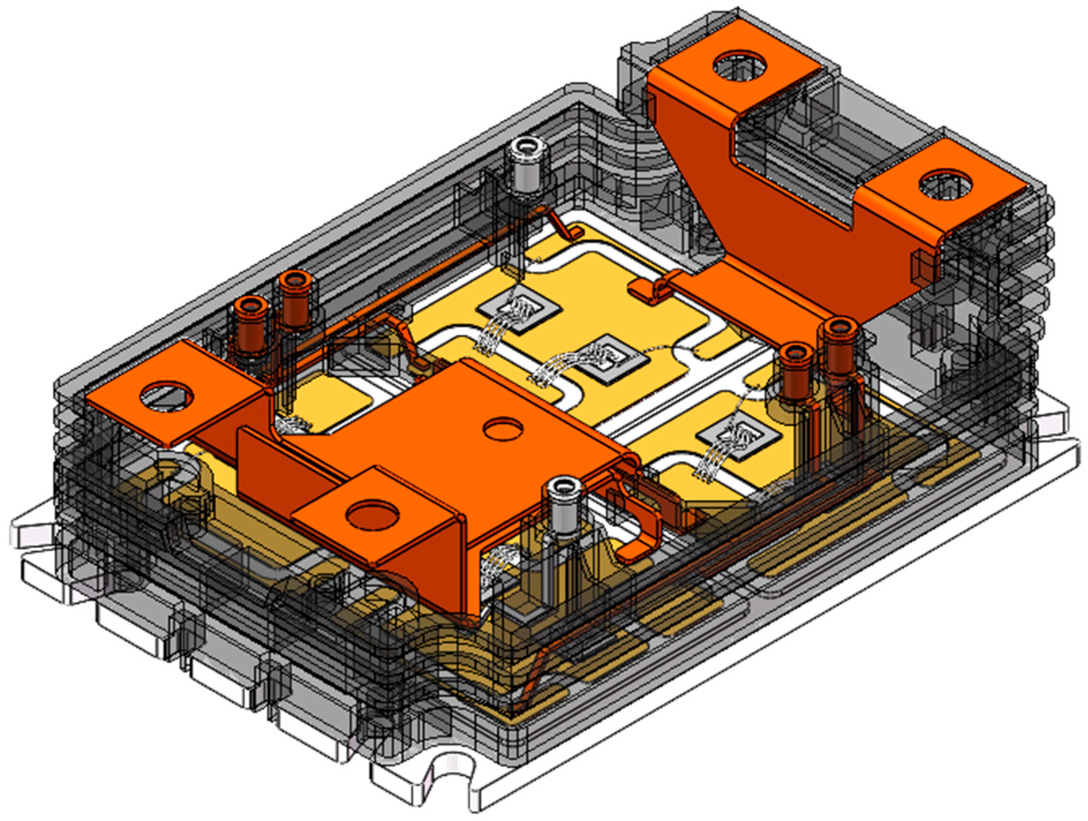
The high-strength plastic housing is adopted in the power module, providing mechanical support for the electrode terminals, along with sealing, moisture resistance, and high-voltage insulation protection. Considering the low-resistance connections and high reliability, each electrode terminal is precisely bonded to the DBC substrate by using ultrasonic welding and the overall internal packaging structure of the proposed module is described in Figure 4.

3. Parasitic and Thermal Performances Evaluation

3.1. Extraction of Parasitic Inductance

In high-voltage power modules, parasitic inductance arises primarily from structural elements such as the copper trace of DBC, bonding wires, and interconnection busbars, along with the mutual coupling between them. During high-frequency switching, rapid voltage transients dv/dt can induce substantial overvoltage across the power chips, oscillations, and excessive electric stress, significantly increasing the risk of device breakdown and compromising the operational reliability of the converter. Therefore, it is critical to quantify the parasitic inductance for accurate performance assessment and design optimization.
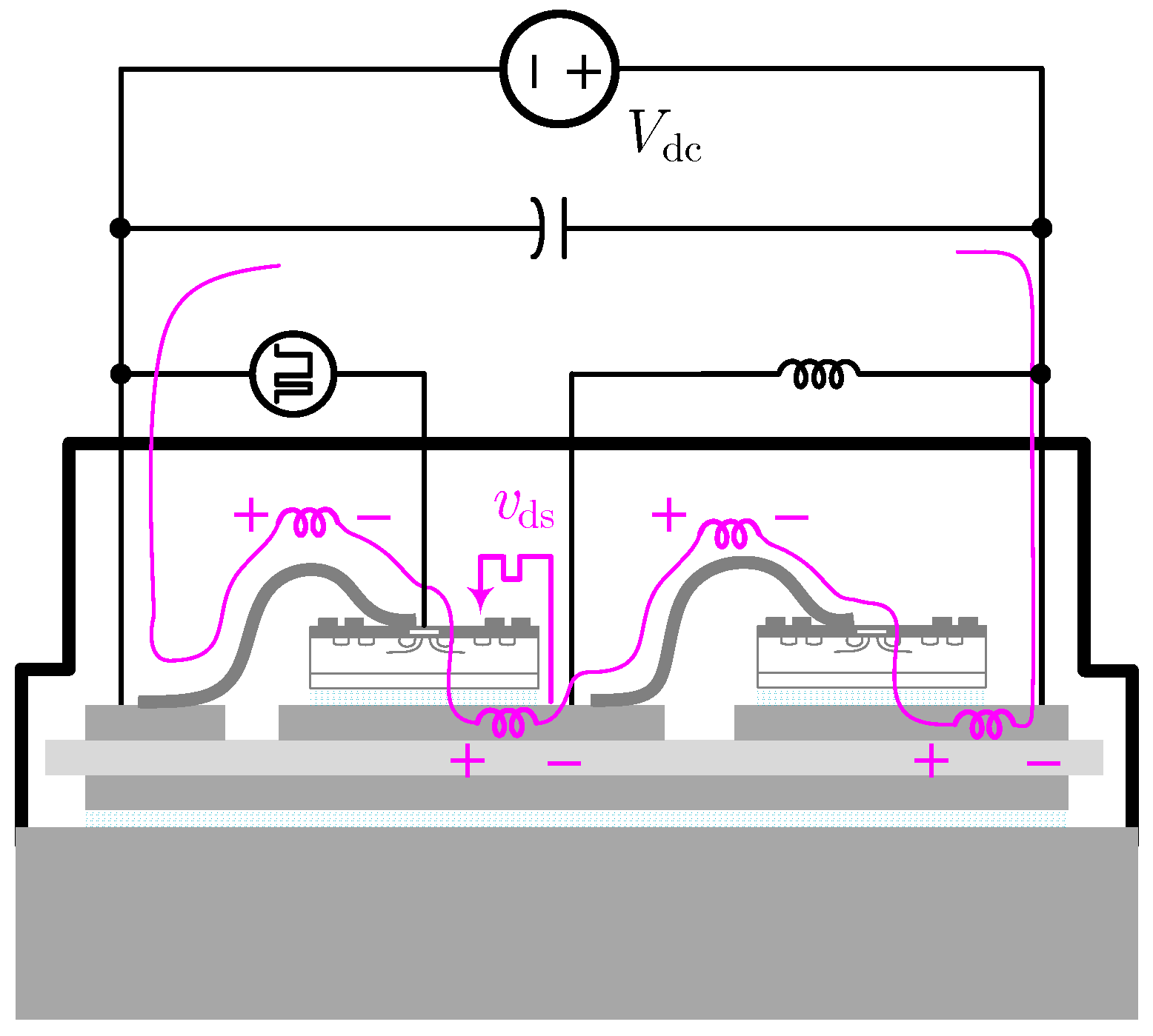
As shown in Figure 5, the parasitic network includes four parts. The first part is from the DC+ terminal to the drain of the high-side chip, while the second part is from the source of the high-side chip to AC terminal. The third part is from the AC terminal to the drain of the low-side chip, and the fourth part is from the source of the low-side chip to the DC− terminal. As a result, the parasitic network Lσ can be expressed as
L σ = L 11 M 12 M 13 M 14 M 21 L 22 M 23 M 24 M 31 M 32 L 33 M 34 M 41 M 42 M 43 L 44
where Lij and Mij represent the self-inductance and mutual inductance of each part of the parasitic network, respectively. Therefore, according to the series-parallel combination rules of parasitic inductance, the total loop parasitic inductance Lσ of the power module can be expressed as
L σ = L 11 + L 22 + L 33 + L 33 + 2 M 12 + M 13 + M 14 + M 23 + M 24 + M 34
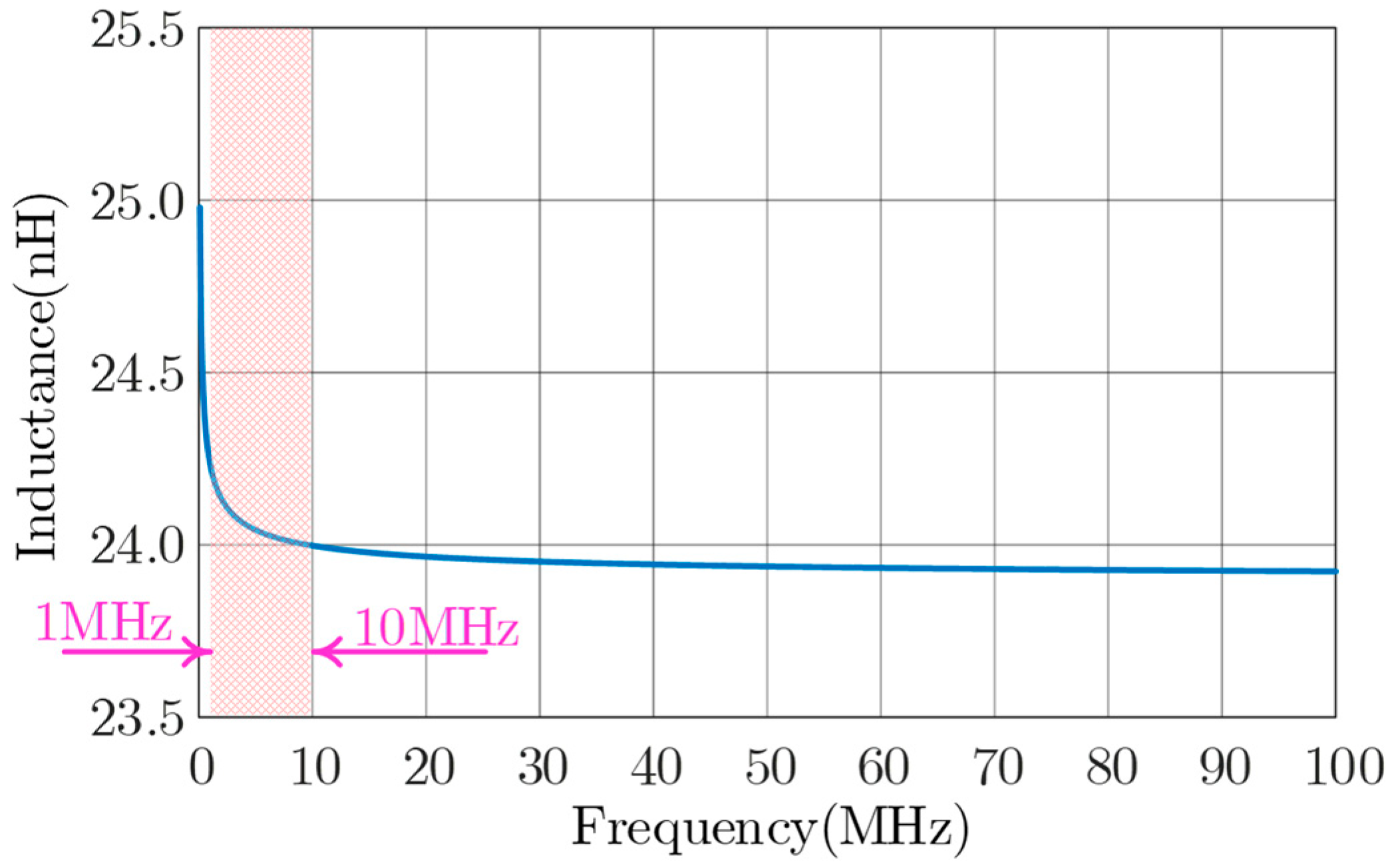
The value of the loop parasitic inductance for the proposed module can be extracted using the finite element analysis software based on ANSYS Q3D Extractor 2023 R1. The frequency-dependent variation in the parasitic inductance is shown in Figure 6. Given that the switching transients of the SiC MOSFET module typically fall within the range of 50–200 ns, corresponding to a frequency domain of 1.75–7 MHz according to signal theory, an extraction frequency of 1 MHz and 10 MHz is selected for subsequent evaluation [26,27,28,29].
At the frequency of 10 MHz, the parasitic inductance can be considered stable and representative of the high-speed switching behavior of the module. The extracted inductance matrix, including both self-inductance and mutual inductance among copper traces in the power loop, is listed in Table 1. Note that the negative parasitic inductances in the off-diagonal elements typically represent mutual inductances between conductors with opposing magnetic field interactions, reflecting the magnetic field cancelation and enhancement effects [30,31]. According to (2) and Table 1, the parasitic inductance of the proposed power module is 24 nH. Similarly, the parasitic inductance at 1 MHz is estimated as 24.3 nH, which differs only slightly from the parasitic inductance at 10 MHz.
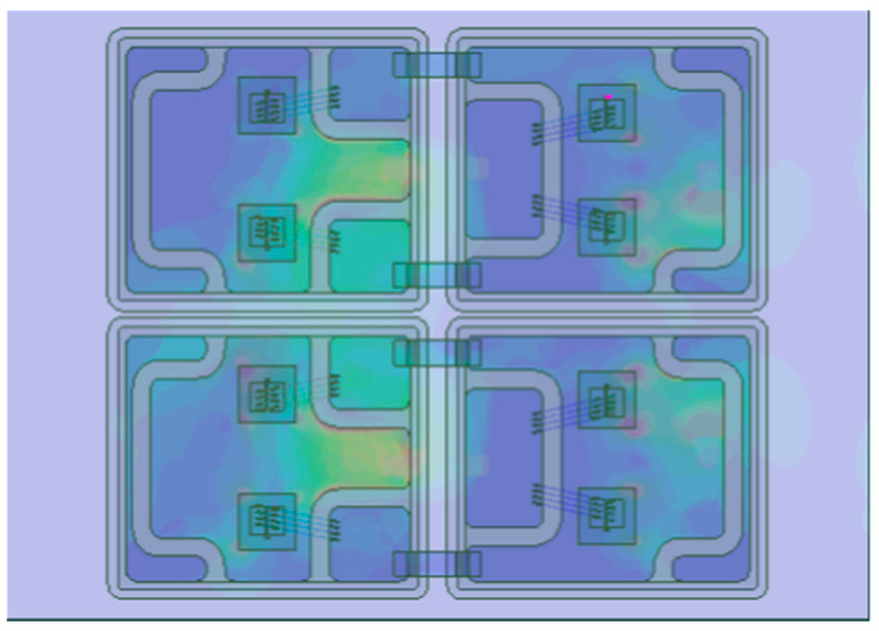
Moreover, the simulated magnetic field intensity distribution is shown in Figure 7. It is noted that the current tends to concentrate along the edges of the copper traces due to the skin effect. Nevertheless, the current distribution across the parallel half-bridge branches remains uniform.

3.2. Extraction of Thermal Impedance

To evaluate the thermal performance of the power module and characterize the efficiency of heat transfer from the PN junction to the ambient, it is essential to predict the junction-to-case thermal resistance Rthjc, which is critical for reliability assessments such as material degradation, solder layer cracking, and bond wire lift-off caused by excessive junction temperatures. In addition, the accurate estimation of Rthjc enables the targeted optimization of the module design, thereby ensuring reliable operation under real-world application conditions. The junction–case thermal resistance can be expressed as
R thjc = T j T a P H
where Tj and Ta are the junction temperature of the chip and the ambient temperature of the power module. PH is the dissipation loss of the chip.
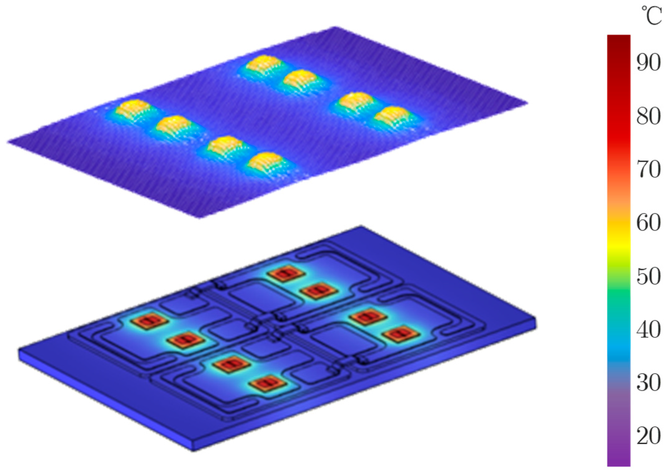
By using COMSOL Multiphysics 6.2, the temperature distribution of the investigated high-voltage power module can be extracted. As depicted in Figure 8, under a single-chip power dissipation of 100 W, the average junction temperature of the parallel chips reaches 71.1 °C. Owing to the relatively sparse layout and large spacing between the paralleled chips, no significant thermal coupling effect is observed, and the temperature variation among the chips remains within 1 °C.
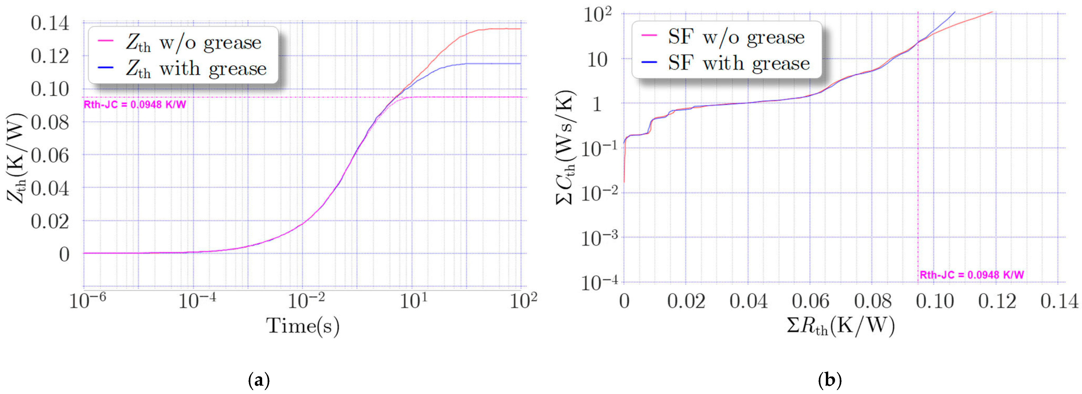
According to the JESD51-14 standard, the junction-to-case thermal resistance is extracted using the transient dual interface method (TDIM) [32]. In this method, the transient thermal response is characterized by applying a power step to the device under test (DUT) and measuring the temperature-sensitive electrical parameter (TSEP), such as the collector-emitter voltage for IGBT and the forward voltage of the body diode for the MOSFET. To perform the TDIM, two measurements are conducted under different thermal interface conditions: one using a high thermal conductivity interface material (e.g., thermal grease), and the other using a low-conductivity interface (e.g., without thermal grease). The two thermal responses are subsequently analyzed by using structure function to determine the junction-to-case thermal resistance. Therefore, to further extract the thermal impedance curve of the power module, two sets of simulations with different boundary conditions were carried out.
First, all paralleled chips within a single switching unit of the phase-leg are modeled as heat sources to simulate the heat generated by power dissipation. A Neumann boundary condition is applied to the bottom surface of the substrate, defined by a convective heat transfer coefficient to represent the thermal interface with the cooling environment. In addition, for all other directions, adiabatic boundary conditions are applied, since the surrounding media (e.g., stagnant air or silicone gel) possess a significantly lower thermal conductivity compared to the internal materials. Finally, two set of simulations are carried out under different boundary conditions—one with thermal grease and the other without—yielding two transient junction temperature rise curves. The temperature profiles are then imported into the Rth evaluator software TDIM-Master 1.0 developed by Infineon. Then, the structure function analysis method was applied to identify the divergence point between the two curves that marks the case boundary, from which the thermal path changes as a result of altered thermal interfaces. The corresponding thermal resistance at the separation point is determined to be the junction-to-case thermal resistance of the module. As shown in Figure 9, the estimated thermal resistance value is 0.0948 K/W.

4. Dynamic Characterization Based on Double-Pulse Test

4.1. Test Platform

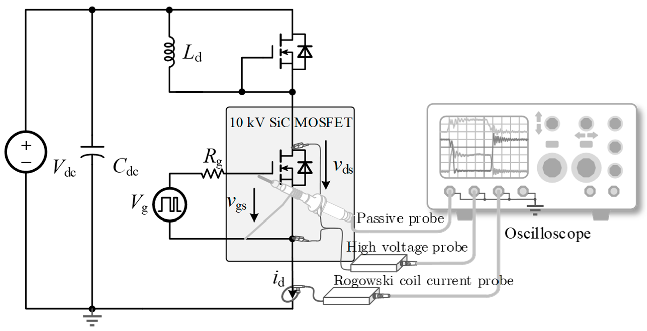
The switching characteristics of the developed 10 kV SiC MOSFET were evaluated based on the double-pulse test platform, and the principle was illustrated in Figure 10. The gate of the upper switch was shorted with its source terminal to keep the switch in the off state. Then, the switching behavior of the lower switch in the half-bridge module was characterized. The gate voltage vgs was measured using a high-bandwidth passive probe, the drain-to-source voltage vds was captured with a 7 kV high-voltage differential probe DP6700 with the bandwidth up to 200 MHz, and the device current ids was obtained via a Rogowski coil placed at the source terminal.
The DC link of the designed double-pulse test was made up of five 2 kV, 95 μF capacitors in series. Static voltage balancing of the capacitors is achieved by connecting resistors in parallel with each capacitor. In terms of load, three 2 mH inductors were connected in series to achieve a high total inductance while minimizing parasitic capacitance. The power module gate bias was switched from −5 V to 18 V with a constant external gate resistance of 10 Ω. The experiments were conducted under the DC link voltage of 6 kV. The test conditions are summarized in Table 2.
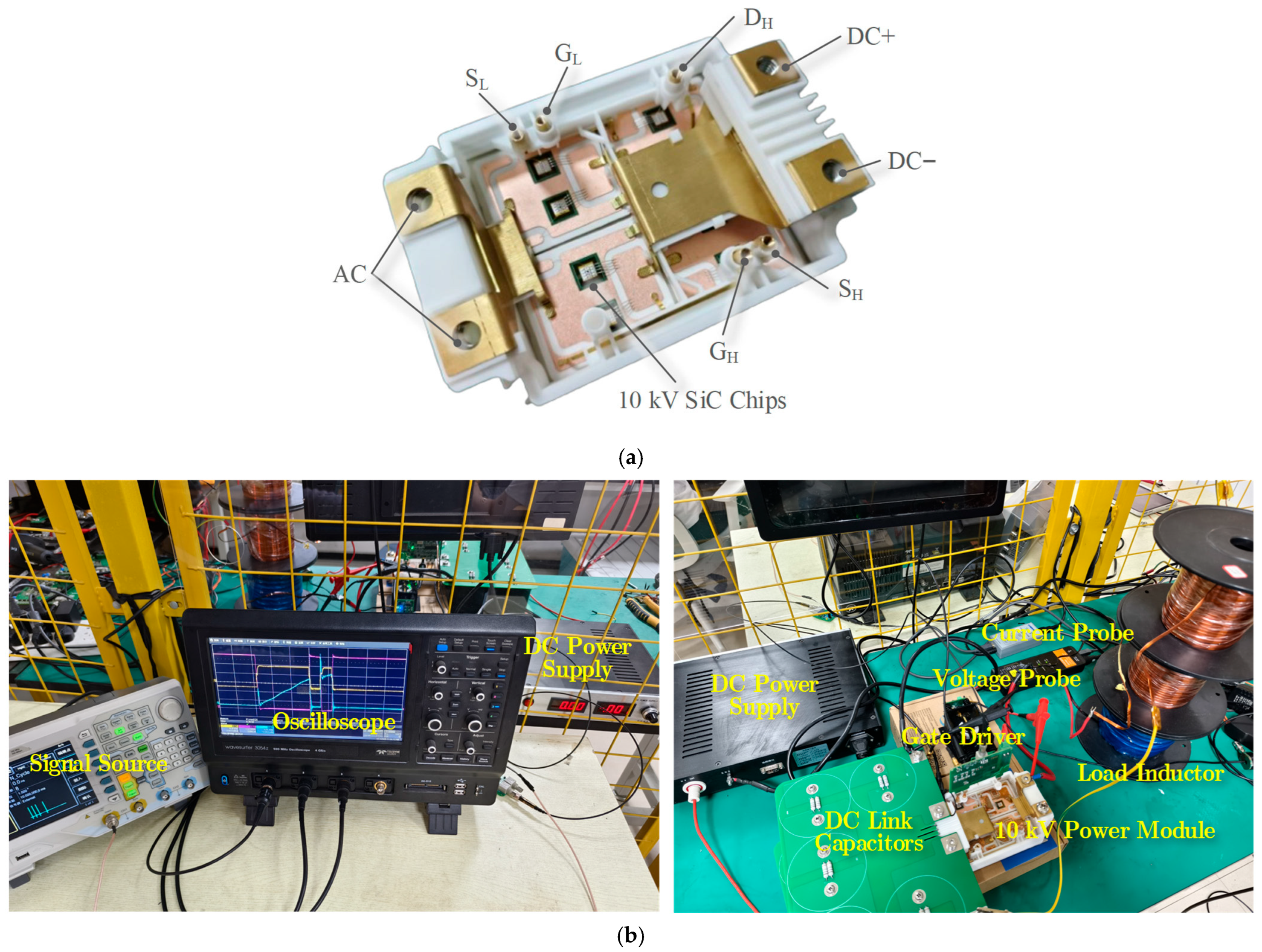
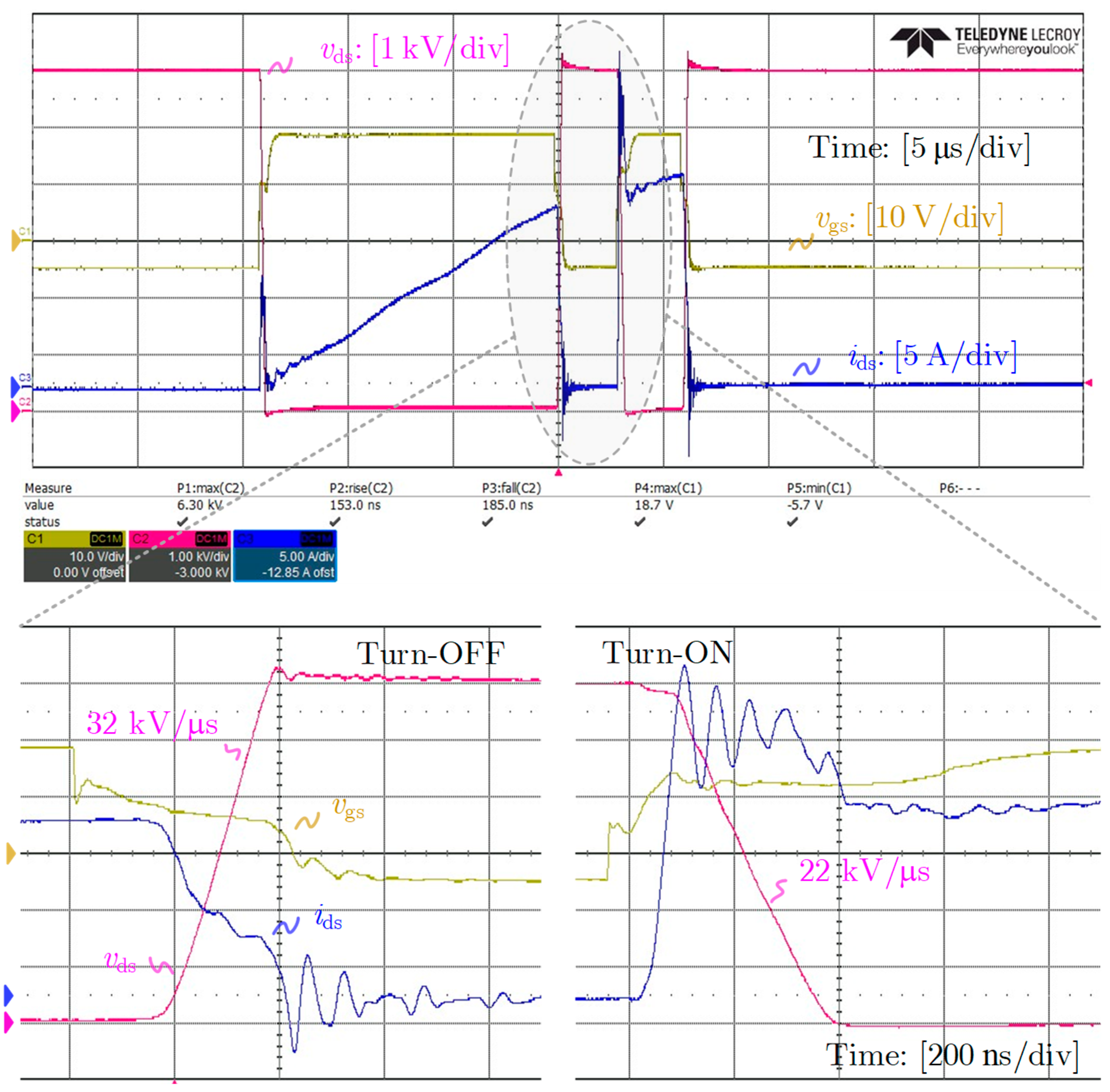
The prototype of the designed 10 kV XHP power module and the double-pulse test platform are shown in Figure 11. The designed 10 kV XHP power module can switch safely under a system voltage of 6 kV. And the switching transient waveforms are shown in Figure 12.

4.2. Experimental Results

During turn-off, the drain-to-source voltage rises at a rate of 32 kV/μs, with a turn-off time of 155 ns (from 10% to 90% DC link voltage). During turn-on, the voltage falls at 22 kV/μs, and the turn-on time is also 235 ns (from 90% to 10% DC link voltage). The high switching speed of the 10 kV SiC device results in significantly reduced switching losses, with a total of 82 mJ calculated according to the guideline from Infineon [33]. Compared to the Si counterpart, the medium-voltage SiC device achieves an approximately 7.5-fold reduction in switching losses [1]. Notably, the voltage overshoot during turn-off is negligible. This is attributed to the relatively small voltage oscillations induced by current transients across the system’s stray inductance, which are insignificant compared to the 6 kV DC bus voltage. This observation suggests that high-voltage, low-current devices are relatively insensitive to packaging and system parasitic inductance.
In contrast, a pronounced current spike is observed during device turn-on. Even during the first switching event, when the inductor current is zero and no reverse recovery occurs, an obvious current overshoot is still present. This spike is caused by the discharge of system parasitic capacitances—including the device output capacitance, and the parasitic capacitance of the package and load inductor—during the turn-on transient. Due to the extra-high dv/dt, high-voltage SiC MOSFETs are highly sensitive to system parasitic capacitance. Therefore, careful optimization of the parasitic capacitance in the system design is essential when implementing power converters based on high-voltage SiC devices.

5. Conclusions

This paper presents the design, implementation, and evaluation of a medium-voltage SiC power module based on a half-bridge topology utilizing XHP packaging. Each switching unit in the module comprises four paralleled 10 kV SiC MOSFET chips arranged in a fully symmetric DBC substrate layout, ensuring uniform current sharing. A laminated busbar is employed for both power and gate signal interconnections, significantly reducing the parasitic loop inductance, which is measured at 24 nH. The distributed chip configuration also improves thermal management by mitigating mutual thermal coupling, resulting in a junction-to-fluid thermal resistance as low as 0.0948 K/W.
The dynamic switching performance of the module was experimentally verified through double-pulse testing under a 6 kV DC-link voltage. The results demonstrate fast and stable switching behavior with no observable oscillation, validating the effectiveness of the proposed packaging strategy. These findings indicate that the developed module offers a compelling solution for next-generation, medium-voltage power conversion systems, supporting further advancements in high-efficiency, high-density commercial SiC-based power electronics.

Author Contributions

Conceptualization, K.X.; methodology, Y.Z.; investigation, S.T.; resources, J.P.; formal analysis and visualization, H.F.; writing—original draft preparation, Y.L.; writing—review and editing as well as project administration, Z.Z. All authors have read and agreed to the published version of the manuscript.

Funding

This research and APC was funded by Industry-University Collaboration Project, Grant No. H20241983.

Data Availability Statement

The data presented in this study are available on request from the corresponding author due to restrictions.

Conflicts of Interest

Authors Kai Xiao, Yining Zhang and Shuming Tan were employed by the company CSG EHV Electric Power, Research Institute, China Southern Power Grid Company Limited, Guangzhou, China. The remaining authors declare that the research was conducted in the absence of any commercial or financial relationships that could be construed as a potential conflict of interest.

References

  1. Johannesson, D.; Nawaz, M.; Ilves, K. Assessment of 10 kV, 100 A Silicon Carbide MOSFET Power Modules. IEEE Trans. Power Electron. 2018, 33, 5215–5225. [Google Scholar] [CrossRef]
  2. Liu, G.; Wu, Y.; Li, K.; Zhang, H. Development of high power SiC devices for rail traction power systems. J. Cryst. Growth 2019, 507, 442–452. [Google Scholar] [CrossRef]
  3. Yang, X.; Li, J.; Ding, Y.; Wang, L. Observation of Transient Parity-Time Symmetry in Electronic Systems. Phys. Rev. Lett. 2022, 128, 065701. [Google Scholar] [CrossRef] [PubMed]
  4. Rothmund, D.; Guillod, T.; Bortis, D.; Kolar, J.W. 99% Efficient 10 kV SiC-Based 7 kV/400 V DC Transformer for Future Data Centers. IEEE J. Emerg. Sel. Top. Power Electron. 2019, 7, 753–767. [Google Scholar] [CrossRef]
  5. Marzoughi, A.; Burgos, R.; Boroyevich, D. Investigating Impact of Emerging Medium-Voltage SiC MOSFETs on Medium-Voltage High-Power Industrial Motor Drives. IEEE J. Emerg. Sel. Top. Power Electron. 2019, 7, 1371–1387. [Google Scholar] [CrossRef]
  6. Vechalapu, K.; Bhattacharya, S. Performance Comparison of 10 kV-15 kV High Voltage SiC Modules and High Voltage Switch Using Series Connected 1.7 kV LV SiC MOSFET Devices. In Proceedings of the 2016 IEEE Energy Conversion Congress and Exposition (ECCE), Milwaukee, WI, USA, 18–22 September 2016. [Google Scholar]
  7. Takahashi, M.; Sun, Z.; Watanabe, A.; Yamamoto, H. Thermo-Mechanical Analysis on 10 kV SiC-MOSFETs to Improve the Reliability of Solder Layers. Microelectron. Reliab. 2025, 172, 115826. [Google Scholar] [CrossRef]
  8. Zhao, S.; Yang, X.; Wu, X.; Liu, G. Investigation on Creep-Fatigue Interaction Failure of Die-Attach Solder Layers in IGBTs Under Power Cycling. IEEE Trans. Power Electron. 2025, 40, 7261–7274. [Google Scholar] [CrossRef]
  9. Ryu, S.-H.; Krishnaswami, S.; O'Loughlin, M.; Richmond, J.; Agarwal, A.; Palmour, J. 10-kV, 123-mΩ·cm2 4H-SiC Power DMOSFETs. IEEE Electron. Device Lett. 2004, 25, 556–558. [Google Scholar] [CrossRef]
  10. Ryu, S.-H.; Krishnaswami, S.; Hull, B.; Richmond, J.; Agarwal, A.; Hefner, A. 10 kV, 5A 4H-SiC Power DMOSFET. In Proceedings of the 2006 IEEE International Symposium on Power Semiconductor Devices and ICs (ISPSD), Naples, Italy, 4–8 June 2006. [Google Scholar]
  11. Callanan, R.; Agarwal, A.K.; Burk, A.A.; Das, M.K.; Hull, B.; Husna, F.; Powell, A.; Richmond, J.; Ryu, S.-H.; Zhang, Q. Recent Progress in SiC DMOSFETs and JBS Diodes at Cree. In Proceedings of the 2008 IEEE Industrial Electronics Conference (IECON), Orlando, FL, USA, 10–13 November 2008. [Google Scholar]
  12. Pala, V.; Brunt, E.V.; Cheng, L.; O’Loughlin, M.; Richmond, J.; Burk, A.; Allen, S.T.; Grider, D.; Palmour, J.W.; Scozzie, C.J. 10 kV and 15 kV Silicon Carbide Power MOSFETs for Next-Generation Energy Conversion and Transmission Systems. In Proceedings of the 2014 IEEE Energy Conversion Congress and Exposition (ECCE), Pittsburgh, PA, USA, 14–18 September 2014. [Google Scholar]
  13. Nielsen, M.R.; Kjær, M.; Zhao, H.; Bech, M.M.; Munk-Nielsen, S. Comparison of Two Third-Generation 10 kV SiC MOSFET Die’s Switching Performance on a System Level. In Proceedings of the 2024 IEEE 10th International Power Electronics and Motion Control Conference (IPEMC-ECCE Asia), Chengdu, China, 17–20 May 2024. [Google Scholar]
  14. Passmore, B.; Cole, Z.; McGee, B.; Wells, M.; Stabach, J.; Bradshaw, J. The Next Generation of High Voltage (10 kV) Silicon Carbide Power Modules. In Proceedings of the 2016 IEEE Workshop on Wide Bandgap Power Devices and Applications (WiPDA), Fayetteville, AR, USA, 7–9 November 2016. [Google Scholar]
  15. Mocevic, S.; Yu, J.; Xu, Y.; Stewart, J.; Wang, J.; Cvetkovic, I.; Dong, D.; Burgos, R.; Boroyevich, D. Power Cell Design and Assessment Methodology Based on a High-Current 10-kV SiC MOSFET Half-Bridge Module. IEEE J. Emerg. Sel. Top. Power Electron. 2021, 9, 3916–3935. [Google Scholar] [CrossRef]
  16. Reigosa, P.D.; Iannuzzo, F.; Munk-Nielsen, S.; Blaabjerg, F. New Layout Concepts in MW-Scale IGBT Modules for Higher Robustness During Normal and Abnormal Operations. In Proceedings of the 2016 IEEE Applied Power Electronics Conference and Exposition (APEC), Long Beach, CA, USA, 20–24 March 2016; pp. 288–294. [Google Scholar]
  17. Wu, R.; Smirnova, L.; Wang, H.; Iannuzzo, F.; Blaabjerg, F. Comprehensive Investigation on Current Imbalance Among Parallel Chips Inside MW-Scale IGBT Power Modules. In Proceedings of the 2015 9th International Conference on Power Electronics and ECCE Asia (ICPE-ECCE Asia), Seoul, Republic of Korea, 1–5 June 2015; pp. 850–856. [Google Scholar]
  18. DiMarino, C.M.; Mouawad, B.; Johnson, C.M.; Boroyevich, D.; Burgos, R. 10-kV SiC MOSFET Power Module with Reduced Common-Mode Noise and Electric Field. IEEE Trans. Power Electron. 2020, 35, 6050–6060. [Google Scholar] [CrossRef]
  19. Jørgensen, A.B.; Christensen, N.; Dalal, D.N.; Sønderskov, S.D.; Bęczkowski, S.; Uhrenfeldt, C.; Munk-Nielsen, S. Reduction of Parasitic Capacitance in 10 kV SiC MOSFET Power Modules Using 3D FEM. In Proceedings of the 2017 19th European Conference on Power Electronics and Applications (EPE’17 ECCE Europe), Warsaw, Poland, 11–14 September 2017; pp. P.1–P.8. [Google Scholar]
  20. Hebedean, C.; Munteanu, C.; Racasan, A.; Pacurar, C. Parasitic Capacitance Removal with an Embedded Ground Layer. In Proceedings of the EUROCON 2013, Zagreb, Croatia, 1–4 July 2013; pp. 1886–1891. [Google Scholar]
  21. Li, X.; Chen, Y.; Chen, H.; Paul, R.; Song, X.; Mantooth, H.A. A 10 kV SiC MOSFET Power Module with Optimized System Interface and Electric Field Distribution. IEEE Trans. Power Electron. 2024, 39, 9540–9553. [Google Scholar] [CrossRef]
  22. Wang, L.; Gong, J.; Long, T.; Blaabjerg, F.; Hu, B.; Wang, Y.; Zeng, Z. Direct Metallization-Based DBC-Free Power Modules for Near-Junction Water Cooling: Analysis and Experimental Comparison. IEEE Trans. Power Electron. 2024, 39, 7052–7063. [Google Scholar] [CrossRef]
  23. Li, Y.; ul-Hassan, M.; Mirza, A.B.; Xie, Y.; Deng, S.; Vala, S.; Luo, F.; Feng, X.; Narumanchi, S.; Flicker, J. State-of-the-Art Medium- and High-Voltage Silicon Carbide Power Modules, Challenges and Mitigation Techniques: A Review. IEEE Trans. Compon. Packag. Manuf. Technol. 2024, 14, 2177–2195. [Google Scholar] [CrossRef]
  24. Infineon Technologies, AG. XHP™ IGBT Modules. Available online: https://www.infineon.com/cms/en/product/power/igbt/igbt-modules/xhp/ (accessed on 23 June 2025).
  25. Defining the Future of IGBT High-Power Modules; Electronics Maker: New Delhi, India, 9 April 2015. Available online: https://electronicsmaker.com/defining-the-future-of-igbt-high-power-modules (accessed on 2 August 2025).
  26. Wang, X.; Chen, Y.; Zhu, W.; Xin, L.; Yang, T.; Sun, K.; Shao, Q.; Chen, Z.; Zhou, S.; Kou, C. Three-Level Parallel Structure Based on XHP Packaging Device and Converter Equipment. CN Patent 216437080U, 3 May 2022. [Google Scholar]
  27. Zhu, A.; Gao, H.; Xia, Y.; Wu, X.; Huang, A.; Peng, C. Adaptive Stray Inductance Extraction Algorithm Using Linear Regression for Power Module with High Noise Immunity and Accuracy. CPSS Trans. Power Electron. Appl. 2022, 7, 176–185. [Google Scholar] [CrossRef]
  28. Zhang, Z.; Guo, B.; Wang, F.; Liu, J.; Wang, H. Methodology for Switching Characterization Evaluation of Wide Band-Gap Devices in a Phase-Leg Configuration. In Proceedings of the 2014 IEEE Applied Power Electronics Conference and Exposition (APEC), Fort Worth, TX, USA, 16–20 March 2014; pp. 2534–2541. [Google Scholar]
  29. Hall, S.H. High-Speed Digital System Design: A Handbook of Interconnect Theory and Design Practices; Wiley-Interscience: New York, NY, USA, 2000. [Google Scholar]
  30. Li, W.; Mao, S.; Wang, Z.; Liu, H.; Yang, J. Modeling and Analysis of the Switching Characteristics Difference for Paralleling SiC MOSFETs in Multichip Power Modules. In Proceedings of the 2021 IEEE Workshop on Wide Bandgap Power Devices and Applications in Asia (WiPDA Asia), Shenzhen, China, 23–25 August 2021; pp. 217–223. [Google Scholar]
  31. Li, W.; Mao, S.; Liu, H.; Yang, J.; Wang, Z. Current Uniformity Optimization of Multi-Chip SiC Module for High-Power Applications. In Proceedings of the 2022 IEEE International Power Electronics and Application Conference and Exposition (PEAC), Wuhan, China, 4–7 November 2022; pp. 545–550. [Google Scholar]
  32. JESD 51–14; Transient Dual Interface Test Method for the Measurement of the Thermal Resistance Junction-to-Case of Semiconductor Devices with Heat Flow Through a Single Path. JEDEC Solid State Technology Association: Arlington, VA, USA, 2010.
  33. Andreas, V.; Hornkamp, M. IGBT Modules: Technologies, Driver and Application; Infineon Technologies AG: Munich, Germany, 2012. [Google Scholar]
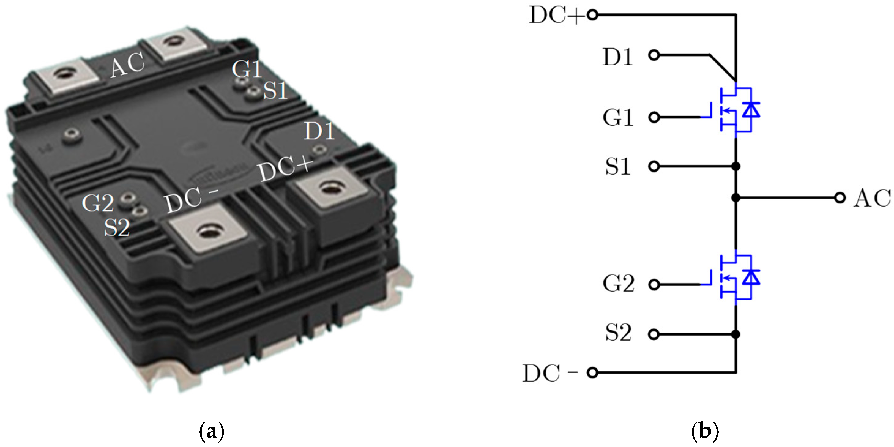
Figure 1. Schematic of the studied power module. (a) Configurations. (b) Circuit topology.
Energies 18 04407 g001
Figure 2. DBC layout and chip arrangement for the proposed module. (a) Upper bridge leg. (b) Lower bridge leg. (c) Overall configuration.
Energies 18 04407 g002
Figure 3. Electrode terminal structure of proposed module. (a) Power terminal. (b) Signal terminal.
Energies 18 04407 g003
Figure 4. Internal packaging structure of proposed module.
Energies 18 04407 g004
Figure 5. Schematic of half-bridge circuit considering parasitic inductance.
Energies 18 04407 g005
Figure 6. Parasitic inductance influenced by frequency of proposed module.
Energies 18 04407 g006
Figure 7. Electro-magnetic field distribution of proposed module.
Energies 18 04407 g007
Figure 8. Simulation result of temperature field distribution of proposed module.
Energies 18 04407 g008
Figure 9. Transient thermal impedance of proposed modules. (a) Zth curves. (b) Structure functions.
Energies 18 04407 g009
Figure 10. Inductance clamp double-pulse testing circuit diagram of module.
Energies 18 04407 g010
Figure 11. High voltage double-pulse test rig. (a) Developed 10 kV XHP power module prototype and (b) test platform.
Energies 18 04407 g011
Figure 12. Experimental results at dc-link voltage 6 kV.
Energies 18 04407 g012
Table 1. Extracted parasitic inductance network at 10 MHz.
Conductor SegmentDC+ to DHSSHS to ACAC to DLSSLS to DC−
DC+ to DHS16.7 nH−0.93 nH0.66 nH7.69 nH
SHS to AC0.39 nH10.91 nH−8.31 nH−0.83 nH
AC to DLS0.66 nH−8.31 nH8.29 nH−0.69 nH
SLS to DC−−7.69 nH−0.83 nH−0.69 nH19.69 nH
Table 2. Experimental conditions of double-pulse test.
ParametersValue
DC Link Capacitors, Cdc10 kV, 19 μF
Load Inductor, Ld6 mH
DC Link Voltage, Vdc7 kV
Gate Voltage (on/off), Vg18/−5 V
Gate Resistance, Rg10 Ω
Disclaimer/Publisher’s Note: The statements, opinions and data contained in all publications are solely those of the individual author(s) and contributor(s) and not of MDPI and/or the editor(s). MDPI and/or the editor(s) disclaim responsibility for any injury to people or property resulting from any ideas, methods, instructions or products referred to in the content.