1. Introduction
Capacitor banks play a crucial role in electrical power systems by serving as a source of reactive power. They act to increase system capacity, support voltage levels, reduce reactive current flow, and mitigate harmonic distortions, thereby improving the stability and reliability of power systems [
1,
2]. Additionally, capacitors are essential components in filter solutions that reduce harmonic content, ensuring an undistorted sinusoidal voltage. This minimizes disturbances in production equipment, measurement errors, and malfunctions in relay protection, while extending the service life of connected equipment [
3]. However, despite their important functions, capacitor banks can introduce high levels of inrush currents during switching. The study of transient disturbances caused by power capacitor bank switching began in the 1950s [
4,
5,
6]. Since then, numerous studies have been conducted to understand and mitigate the effects of switching power capacitor banks. These studies use advanced simulation tools, such as the ATP, and, more recently, integrate Artificial Intelligence (AI) techniques to optimize operations and reduce the impacts that transient currents cause to the system [
7,
8,
9].
When a capacitor bank is inserted into an electrical circuit, a transient phenomenon occurs, affecting both the current and voltage of the system [
10]. The severity of this phenomenon increases when a residual voltage remains at the bank terminals. For instance, a residual voltage equivalent to 10% of the nominal voltage’s peak value can elevate transient voltage and current by 10% [
11]. To mitigate these effects, IEEE (Institute of Electrical and Electronics Engineers) Standard 18 [
12] determines that capacitors should incorporate internal discharge resistors capable of reducing residual voltage to 50 V or less within 5 min. This configuration ensures that the capacitor bank is sufficiently discharged before energization, minimizing risks to system integrity and equipment. Despite these safeguards, energizing a fully discharged capacitor bank remains a major challenge. At the moment of connection, the capacitive reactance of the bank approaches zero, creating a near-short-circuit condition. This results in steep current gradients and voltage oscillations, especially if switching occurs at non-ideal phase angles.
To mitigate these effects, techniques such as preinsertion reactors, arresters, CSD, and preinsertion resistors (PIR) have been developed [
13,
14,
15,
16]. Among them, the combination of CSD and PIR in circuit breakers appears as a promising solution, as it reduces current peaks and extends the equipment’s service life [
17,
18]. However, the optimal parametrization of the closing instants for both the PIR and main contacts remains a complex challenge, requiring accurate methods to synchronize the operation with the optimum point of the voltage waveform [
1,
19].
In the Brazilian context, field studies conducted by [
20,
21] revealed premature failures in 765 kV autotransformers due to the frequent switching of 200 Mvar capacitor banks. Detailed measurements and simulations identified high inrush current peaks during non-ideal parameterized operations, requiring adjustments in the controlled switching device (CSD) to minimize transients. Further analysis highlighted the importance of adjusting the main contact closing when the busbar and capacitor voltages are equal, emphasizing the need for precise control strategies. However, conventional switching controllers may not have a platform to automatically display waveforms at each switch, which can make it difficult to accurately assess transient behavior. Another detail is that a controlled switching specialist may be required for a solid assessment. Based on this context, this paper presents a computational methodology to help the better setting the parametrization of circuit breakers equipped with PIR and CSD (hybrid techniques). The approach combines analysis of real-world waveforms (collected from a Brazilian substation) and simulated waveforms (via ATP), applying signal processing techniques (filters and derivatives) to identify the best instants for PIR and main contact insertion. In addition, a diagnostic tool based on Python language (version 3.13.2) was developed to propose adjustments that minimize inrush currents and prevent mechanical failures.
This work expands the pioneering efforts of [
9] by proposing an innovative methodology that not only establishes objective criteria to validate the quality of CSD parametrizations, but also presents a computational tool that provides the optimal controlled switching points, ensuring operational safety and energy efficiency in High Voltage (HV) systems.
The studies referenced in this paper have provided valuable insights into controlled switching of capacitor banks, but they did not present an automated methodology to determine the optimal controller parametrization. This work addresses this gap by introducing a computational approach to dynamically identify and recommend the best switching parameters, eliminating the reliance on manual observation.
2. Power Capacitor Bank Switching
Switching of capacitor banks generates transient overvoltages, harmonics, and inrush currents. These transients propagate through the transmission lines connected to the substation, causing disturbances in remote equipment and also in adjacent equipment [
22]. They also cause damage to the capacitor bank itself and to the circuit breaker (degradation of the PIR, main, and arc contacts). This degradation is a major problem and difficult to diagnose, as conventional tests using static resistance measurement often do not identify the problem, requiring a more elaborate test using Dynamic Resistance Measurement (DRS) of contacts [
23].
Inrush currents generated during the energization of a single capacitor bank can reach 5 p.u. with frequencies between 200 and 600 Hz. In a back-to-back configuration, which occurs when capacitors are combined on the same busbar to increase reactive compensation capacity, the levels of transient currents can be much higher. This occurs when a neighboring charged capacitor bank discharges on the bank being inserted into the electrical circuit. In this configuration, the inrush current generated at the moment of bank energization can reach 40 to 100 p.u. with frequencies in the order of kHz [
17,
24,
25].
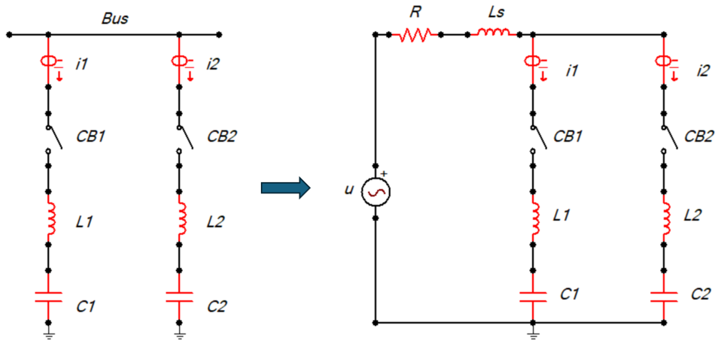
Figure 1 presents a general single-phase equivalent circuit used to describe the phenomena associated with the switching of capacitor banks. Two capacitor banks (C1 and C2) are connected in a back-to-back configuration to a busbar. L1 and L2 represent the stray inductances of the capacitors, which can be ignored since the system inductance (Ls) is typically much higher.
where
u: Source voltage.
: System inductance.
R: Resistance of the circuit.
: Circuit breaker under analysis.
: Circuit breaker, open for single switching, closed for back-to-back condition.
: Current through capacitor bank C1.
: Current through capacitor bank C2.
: Stray inductance C1.
: Stray inductance C2.
: Capacitor bank 1.
: Capacitor bank 2.
Single capacitor bank switching occurs when is energized, while is de-energized. In this scenario, the equivalent circuit consists of the system inductance () in series with capacitor 1 (). The stray inductance can be ignored because .
The energization of when is already connected to the busbar and charged will generate higher levels of inrush current due to the inrush current associated with charging of supplied by . This configuration is called back-to-back energization.
For both single and back-to-back switching, several factors must be considered, as they significantly influence the magnitude and frequency of inrush current. These parameters include the voltage closing angle, capacitances, inductances, load on the capacitor bank, and the circuit damping [
15].
The following equations govern the behavior of the inrush current and frequency at the moment of switching of the capacitor bank.
2.1. Single Capacitor Banks Switching Equations
Applying Kirchhoff’s law to the circuit shown in the
Figure 1 results in Equation (
1).
where
u is the source voltage (V).
R is the resistance (losses in the circuit or PIR) ().
is the inrush current (A).
L is the inductance total of the circuit () (H).
is the capacitance of capacitor bank 1 (F).
Differentiating the equation and considering that the circuit is switched at the voltage peak (where
), then dividing all terms by
L, yields the following expression:
Equation (
2) is a second-order linear differential equation that has three possible solutions, which vary according to the damping level in the circuit, affected by the value of
R. Taking
and
, the three possible solutions correspond to Equations (
3)–(
5).
- 1.
- 2.
Critically damped
- 3.
For circuit breakers equipped with PIR, Equations (
3) and (
4) can be applied.
2.2. Back-to-Back Switching Equations
In a back-to-back energization of capacitor banks, the inrush current of the bank to be energized will be increased by the loaded banks connected to the same busbar.
Considering capacitor bank
is already energized (
Figure 1), the moment energizing bank
occurs,
will contribute to the energy supply, with the peak and frequency of the inrush current being limited by the inductances
and
, since the bank in question
is discharged. In this back-to-back condition, where a capacitor bank already inserted in the system discharges into the other, the equivalent capacitance will be the series capacitance, as shown in Equation (
6):
The behavior of equivalent capacitance and inductance is described by Equations (
7) and (
8), respectively.
The inrush current peak can reach extremely high values due to the potentially small magnitude of
. The frequency of the inrush current is determined by the equivalent inductance and capacitance, as shown in Equation (
9):
Substituting Equations (
7) and (
8) in Equation (
6) results in the final inrush current peak, given by the Equation (
10):
Equations (
7) and (
8) in Equation (
9) produce the final back-to-back frequency, represented by Equation (
11).
3. Transient Mitigation Techniques
To reduce voltage and current transient levels during capacitor bank energizations, there are some methodologies that can be applied, as follows:
- (i)
Preinsertion inductor: When accurately adjusted, it can reduce the voltages and currents that result from back-to-back switching. The dimension of the inductor is related to the level of short-circuit at the specific point. A high short-circuit level results in a low inductive reactance in the system, necessitating larger inductor dimensions to adequately mitigate transient effects [
11,
15,
24].
- (ii)
Surge arresters: These can limit the magnitude of the transient overvoltages and prevent failures in the capacitor bank during a breaker failure or restrike [
16]. Despite the efficiency of arresters in suppressing overvoltages, they have limited response to high frequency oscillation [
26].
- (iii)
Fixed inductors: These are physically different from preinsertion inductors, as they are permanently connected to the capacitor bank. They are effective in limiting inrush and outrush currents caused by faults, but are not as effective in limiting overvoltages. The use of fixed inductors to limit inrush current may generate high-frequency transient recovery voltage (TRV), potentially exceeding standardized TRV limits [
27].
- (iv)
A 6% detuning reactor: This more effectively reduces the transient oscillation, overvoltages, and inrush currents compared to the current limiting reactor. However, it causes distortion in the current and voltage waveforms and an increase in the capacitor bank voltage. The main objective is to limit the inrush current and avoid harmonic amplification. In practice, this technique limits the inrush current to values below 50 times the nominal current of the bank [
7,
28,
29].
- (v)
Preinsertion resistor: This can limit the inrush current level and allow the charge of the capacitor banks to be more smooth, reducing the impact on the electrical system. This device is connected in parallel with the main contact and in series with the capacitor bank. Its operational period is approximately 10 to 15 milliseconds and is bypassed by the main contact after completing its operation. This method is a common practice in power electrical systems to mitigate issues related to inrush current and overvoltage [
13,
14,
15]. Despite the efficiency of the resistor, the PIR adds a set of mechanisms and parts to the circuit breaker, increasing the final cost of the asset by approximately 25% [
30].
- (vi)
Controlled Switching Device: This electronic device synchronizes the closing of circuit breaker contacts with specific points on the voltage waveform, ensuring that the main contact closes when the potential difference between the circuit breaker terminals is close to zero. By precisely controlling the switching instant, the CSD significantly reduces the magnitude of inrush currents during capacitor bank energization [
2]. However, improper configuration of the switching controller can lead to consecutive switching operations at non-ideal points in the waveform and cause damage to assets [
19].
- (vii)
Hybrid method (CSD combined with PIR): Studies show that the implementation of controlled switching in circuit breakers equipped with preinsertion resistors brings benefits that increases the useful life of the capacitor units [
17,
18]; however, it is more complex to determine the optimal closing point of PIR and main contacts, as highlighted by [
1,
19]. Thus, this work presents an automated approach that integrates techniques for detecting the closing moments of the circuit breaker contacts, as well as determining the best points, with the aim of optimizing the switching moment. The methodology presented below details the development of the application.
4. Materials and Methods
The methodology proposed in this work consists of developing a computational solution to analyze the quality of controlled switching (closing) of capacitor banks operated by circuit breakers equipped with PIR. Two scenarios are explored to evaluate the accuracy of the proposed method: one based on real field measurements and the other on simulation-generated waveforms.
- 1.
Real field measurements from a Brazilian substation: Initially, real records were collected from a 200 Mvar, 345 kV power shunt capacitor bank installed in a Brazilian substation. The data has been stored in a database since 2010.
- 2.
ATP files originated from simulation: Subsequently, files were generated from the modeling using the ATP software (version 7.6) based on the real parameters of the capacitor bank under analysis, allowing comparison between real and simulated waveforms, contributing to the validation of the solution and providing flexibility to apply and study parameter changes and switching conditions that are unfeasible in real power systems due to equipment restrictions.
Both sets of files (real field measurements and from ATP) are in the COMTRADE (Common Format for Transient Data Exchange), an international standard developed by the IEEE (Standard C37.111) [
31]. This format is used to record and store oscillographic data of transient events in electrical power systems (EPS). Since the real records were already in COMTRADE format, the simulation data were also generated in this format to ensure standardization across the studies.
The methodology is based on four main steps, as depicted in the flowchart of
Figure 2 and described as follows.
Each step of the methodology is detailed in the following subsections.
4.1. Data Acquisition
Data acquisition was performed by directly measuring the current and voltage signals in the secondaries of the current transformer (CT) and potential transformer (PT), respectively, installed in a Brazilian substation. These signals were interfaced by the Telemulti signal conditioning board and acquired by the Advantech PCI-1713U data acquisition board, which has 32 isolated analog channels, a sampling rate of up to 100 kS/s, and 12-bit resolution, ensuring accuracy and reliability in capture. Data acquisition is triggered whenever a capacitor bank is operated by the circuit breaker. The generated files contain the currents of the three phases and the reference voltage of the busbar, and are organized and identified by the name of the capacitor bank and the date and exact time of operation.
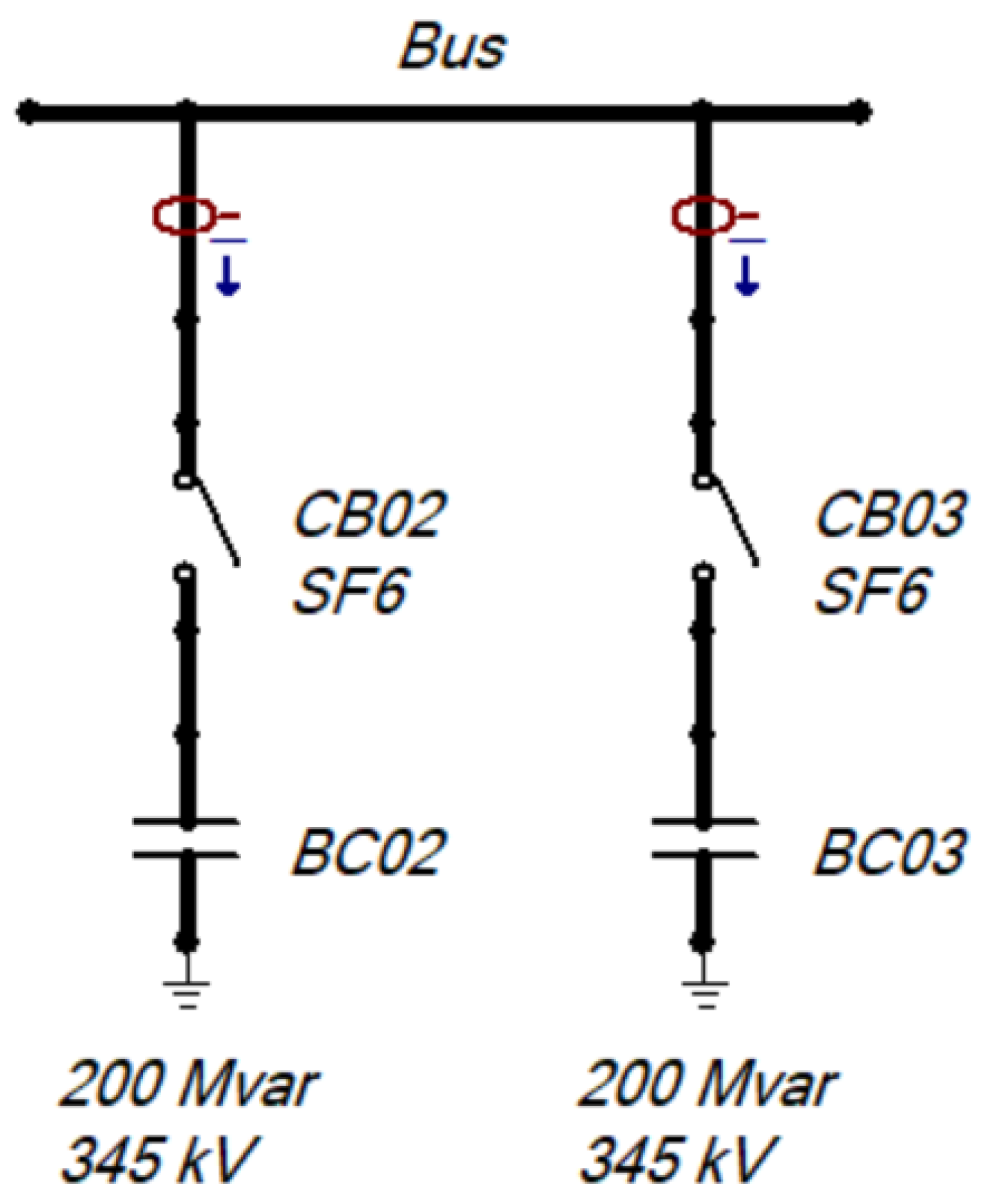
Capacitor bank number 3 (BC03), as demonstrated in
Figure 3, was used for the studies presented in this work. For switching in the back-to-back configuration, bank number 2 (BC02) was considered previously energized.
4.2. Max Inrush Current Measurement, PIR, and Main Points and Preinsertion Time
The maximum value of the inrush current is determined by the highest peak observed during the switching transient, preserving the signal (maximum positive or negative peak). This measurement is performed before applying any treatment to the original signal.
The value of
is given by Equation (
12):
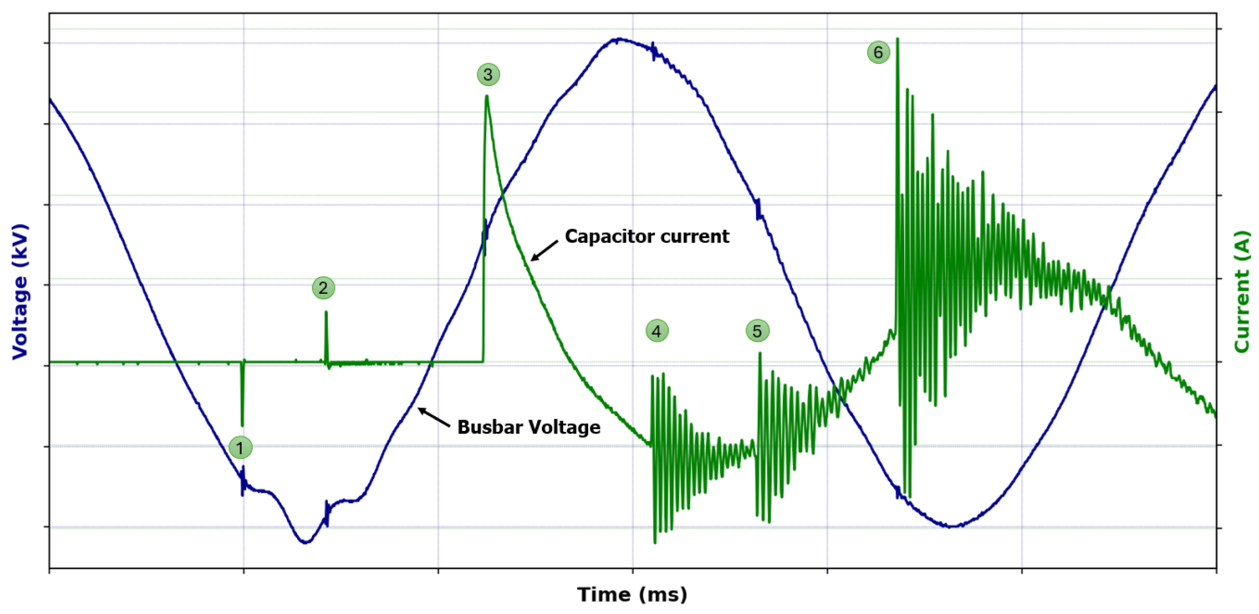
The process of identifying the closing time instants of the PIR and main contacts in this work is undertaken through the application of the dI/dt derivative, where the occurrence of the two highest current variations will determine these points. The method was implemented in the Python programming language. In a real energy environment, switching operations are often subject to electromagnetic interference and high noise levels, originating from other equipment or even from adjacent phases, as can be seen in
Figure 4.
where
Point 1: Phase A PIR insertion point.
Point 2: Phase B PIR insertion point.
Point 3: Phase C PIR insertion point.
Point 4: Phase A main contact insertion point.
Point 5: Phase B main contact insertion point.
Point 6: Phase C main contact insertion point.
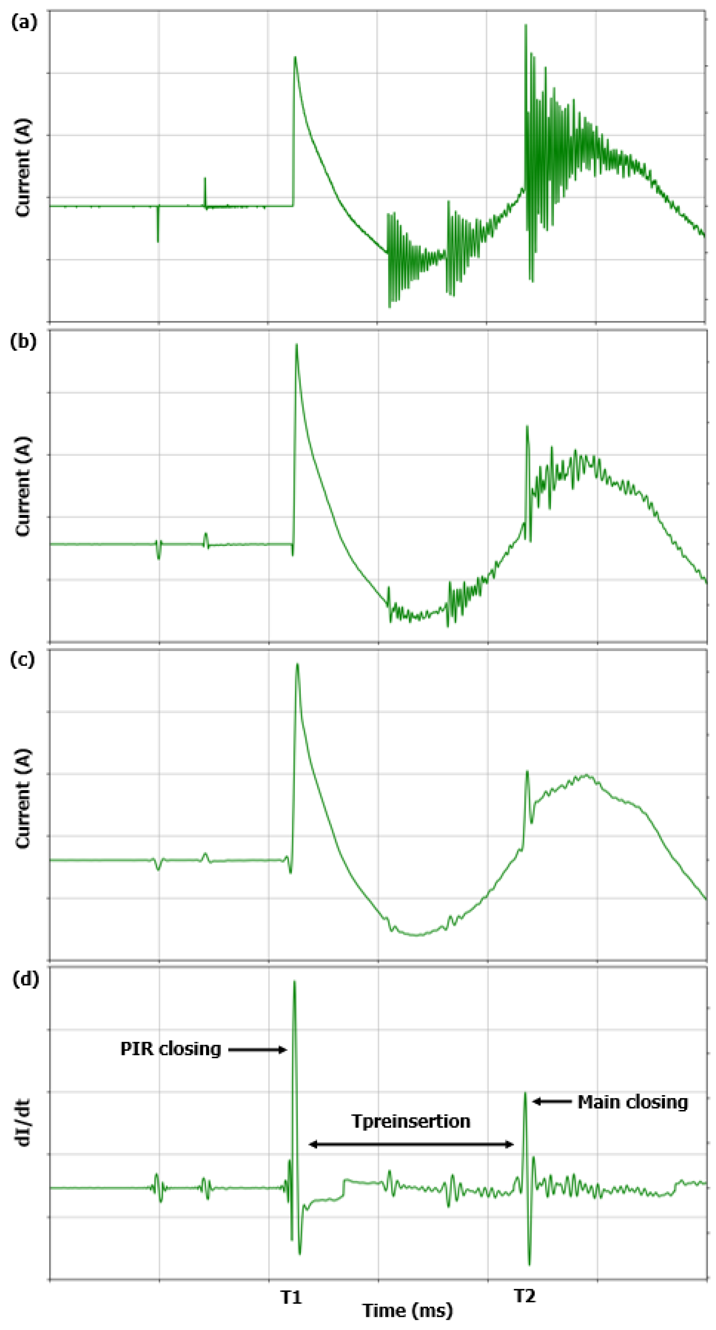
Applying the derivative directly to the current signal does not produce good results due to the noise present in the signal. To improve signal quality and highlight the points of interest (PIR and main contacts insertion instants), processing followed a three-step approach. First, a Savitzky–Golay filter was applied to smooth the signal and reduce high-frequency noise. Next, a low-pass Butterworth filter was used, which eliminates unwanted components of the signal without causing significant phase distortions. Finally, the gradient derivative was calculated to detect abrupt variations in the current signal, which allowed identifying with good accuracy the moments at which the PIR and main contacts were closed.
4.2.1. Filtering
To reduce high-frequency noise in the current signal while preserving its peaks and main trends, was applied a Savitzky–Golay filter [
32] with a 21-point window and third-order polynomial. This configuration was chosen as it provides a good balance between effective smoothing and preservation of the signal’s characteristics. Larger windows can distort the original signal characteristics and introduce phase shifts in the measured angles, while smaller windows are insufficient to effectively attenuate fast transients. The 21-point window represents a compromise that maintains signal fidelity while achieving satisfactory noise reduction in the historical files under study.
The main function of this first filter was to reduce fast front noises caused by the closure of adjacent phases and reflected in the signal under analysis. For example, points 1 and 2 in
Figure 4 were caused by the closure of the PIRs of phases A and B. The application of this first filter attenuates these noises, improving the signal for the correct detection of the PIR of the phase under analysis.
To enhance the detection of switching transients while preserving signal integrity, a 4th-order Butterworth filter [
33] with a cutoff frequency (
) was applied. This filter was selected for its maximally flat pass-band response, ensuring minimal distortion of the inrush current waveform during the transient phase, which is a critical requirement for accurately identifying PIR and main contact closing instants.
The values for cutoff frequency () and filter order () were defined based on practical tests and observations, ensuring effective attenuation of unwanted components, preserving the transient signal characteristics.
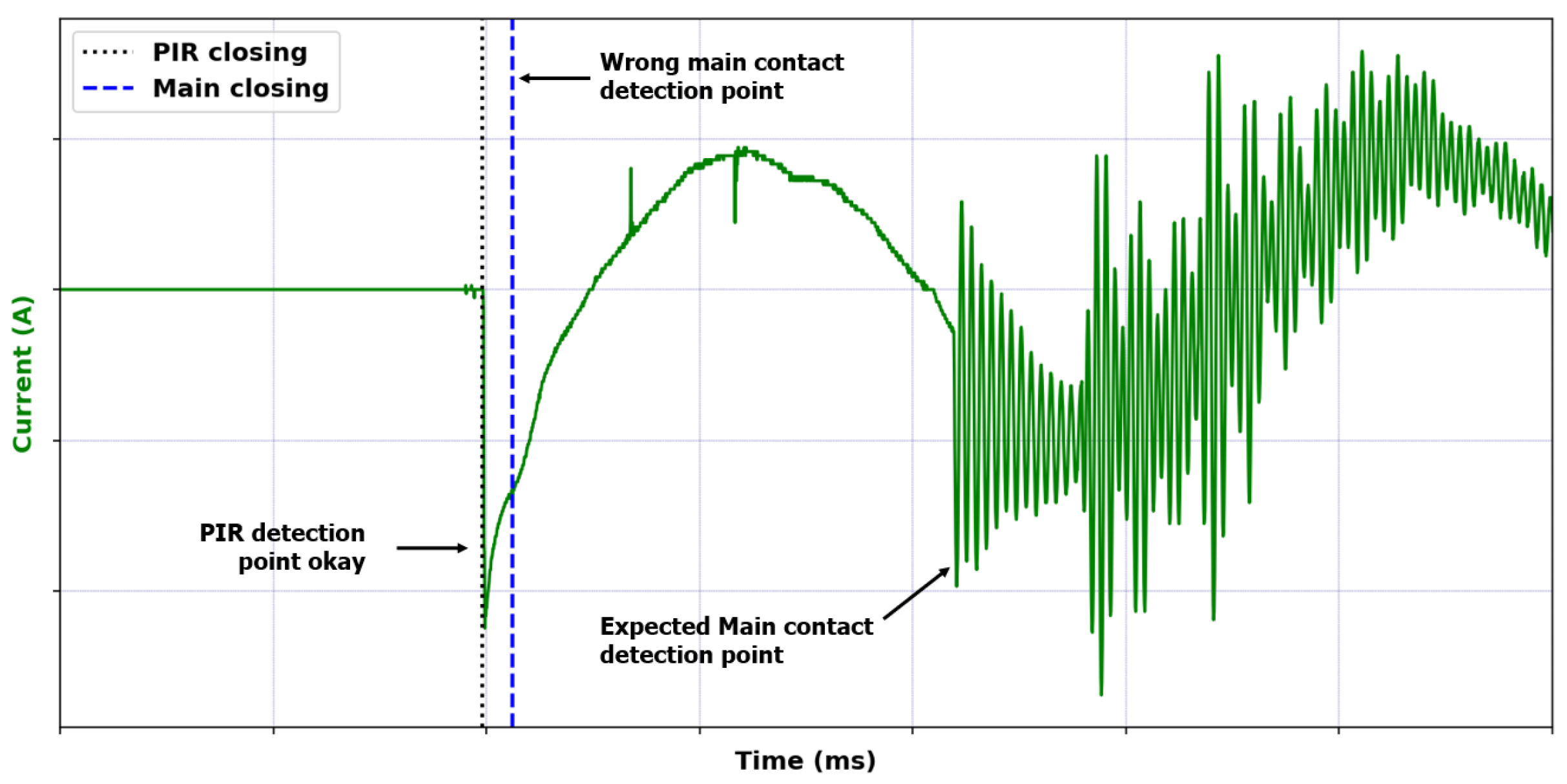
For the files analyzed in this work, frequency values below 2000 Hz compromise the correct identification of the main contact, as they eliminate important signals that occur during the closing of this contact, as can be observed in
Figure 5.
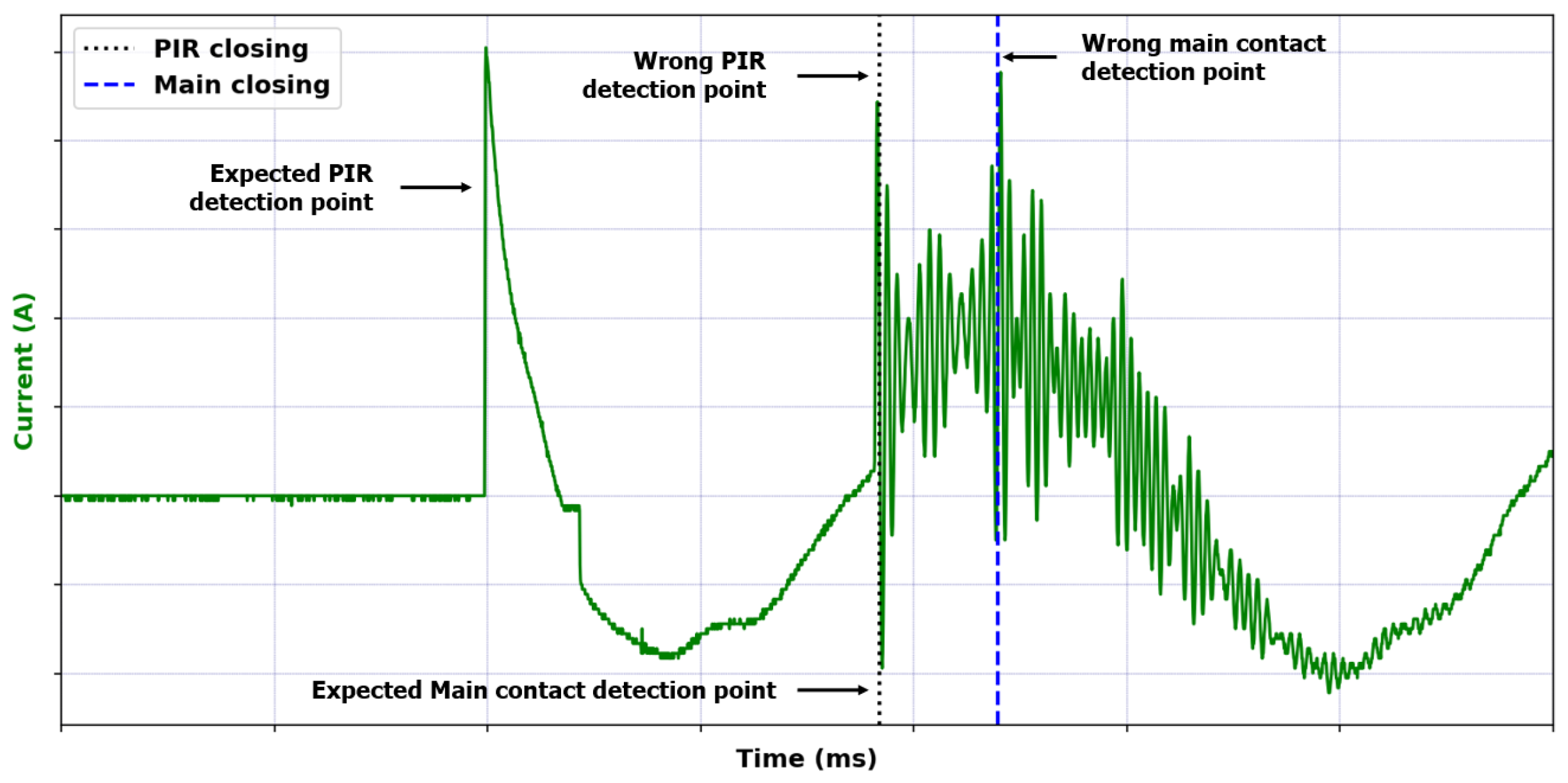
On the other hand, setting high values for the cutoff frequency (for example, 5 or 6 kHz) can cause errors in both the PIR and the main contact detection, as can be seen in
Figure 6.
4.2.2. Gradient Derivative
The double-filtered signal, first processed using a Savitzky–Golay filter and then refined with a Butterworth filter, was analyzed using the gradient method (Equation (
13)) to compute the derivative (
).
where
is the value of the array at position .
is the value of the array at position .
h is the interval between adjacent points.
Figure 7 presents four waveforms that illustrate the analysis process to identify the moments when the PIR and main contacts close in a capacitor bank switching. The first waveform (a) corresponds to the original signal (raw current), without any treatment, showing the current transients in a back-to-back switching. The second waveform (b) presents the result of the application of a Savitzky–Golay filter with a window of 21 points and polynomial order 3, which smooths the signal, reducing high-frequency components that may interfere with the identification of the time instants of the circuit breaker contacts closing. The third curve (c) shows the signal after the application of a 4th-order Butterworth filter with cutoff frequency = 3000 Hz. Finally, the fourth waveform (d) displays the result of the application of the gradient derivative (
), which highlights the abrupt variations in the current, allowing the clear identification of the contact insertion points: the first (left to right) corresponding to the closing of the PIR and the second associated with the closing of the main contact of the circuit breaker.
As shown in
Figure 7, the PIR closing instant (
) corresponds to the first significant peak in
, reflecting the abrupt current rise when the resistor is inserted. The main contact closing instant (
) is identified by detecting the second significant peak in the current derivative, which corresponds to the moment when the main contact closes, bypassing the resistor and allowing full current flow.
To measure the preinsertion time (
), which corresponds to the time difference between the closing of the main contact (
) and the PIR (
), the calculation was performed using the Equation (
14).
The time between PIR closing () and main contact closing () must be within the declared range. High deviations (up or down) may indicate mechanical problems in the resistor or electrical issues in the circuit breaker itself. This measurement is essential to identify potential anomalies and ensure the circuit breaker operates within the parameters specified by the manufacturer.
4.3. Best Point for Main Contact and Proposed Adjustment
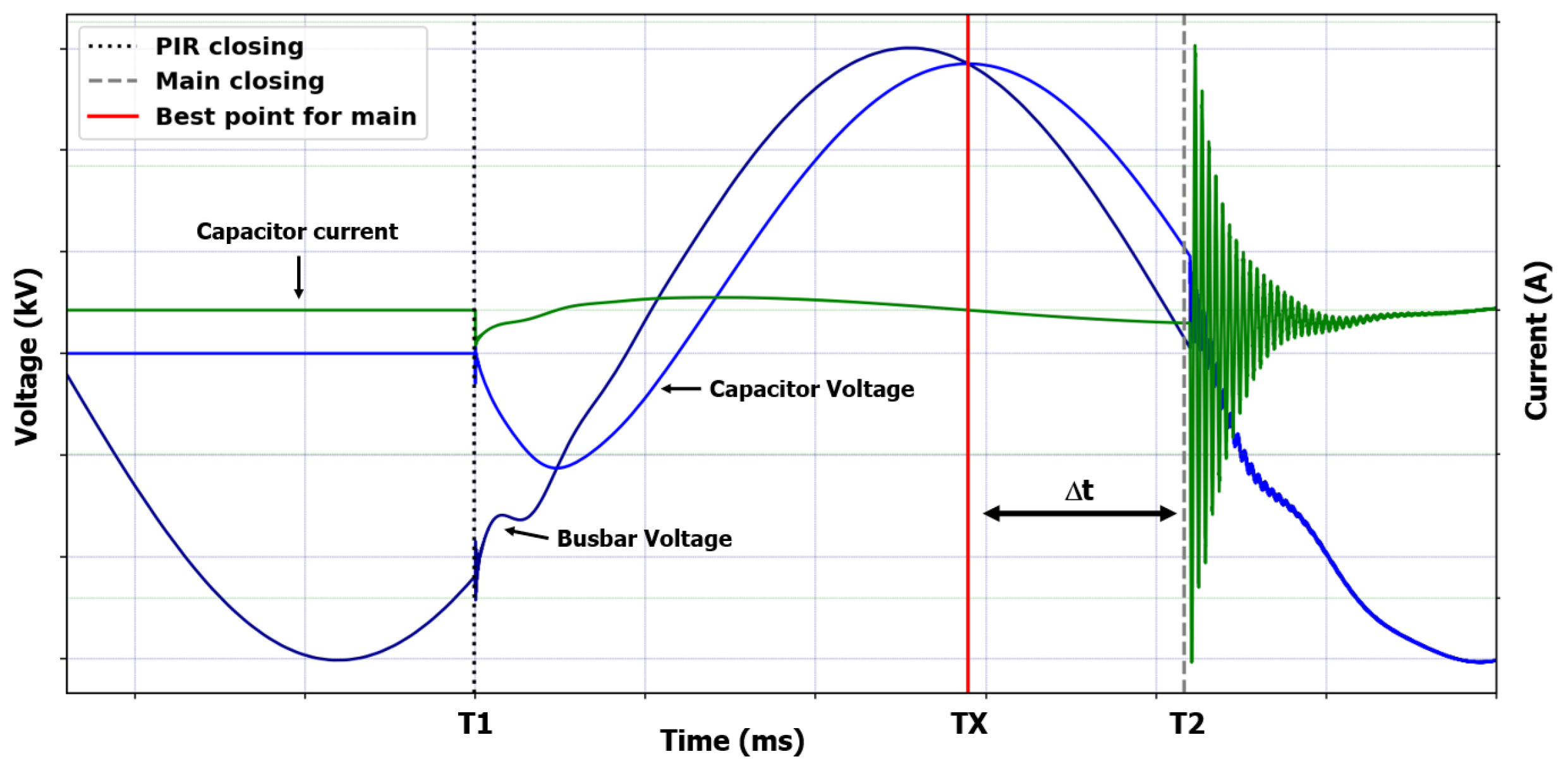
Based on the identification of the main contact insertion instant (as detailed in the previous section), it is possible to determine its best closing time instant, which occurs at the previous zero current crossing point when the busbar and capacitor voltages are of the same amplitude, as can be seen at point (
) in
Figure 8. Closing the main contact at this point ensures smooth switching with the lowest possible levels of inrush current.
The proposed reparametrization (adjustment) presented as
corresponds to the time difference between the real instant of the main contact’s insertion (
) and its optimal closing point (
), as defined by the Equation (
15). This value is automatically calculated and displayed by the application.
4.4. Modeling and Simulation in ATP
To evaluate the effectiveness of the proposed solution, capacitor bank 03 (BC03 in
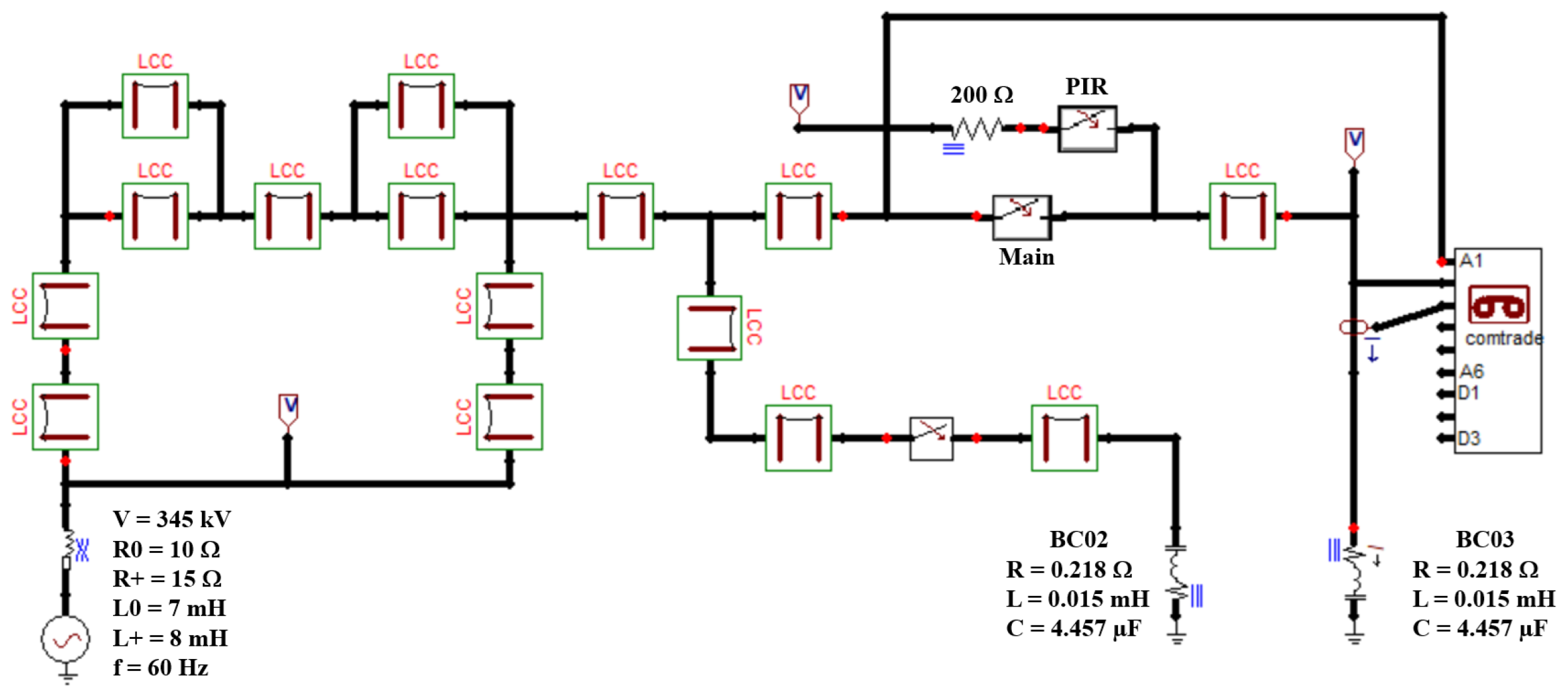
Figure 3) was modeled using real parameters of the Brazilian substation under study in order to simulate a first condition with switching in unfavorable conditions, according to real waveforms extracted from historical field records, and to subsequently simulate a second condition, with the main contact insertion point defined by the methodology in order to have a comparison of the inrush current levels between what the original waveform presents and how it is after optimization. The use of ATP in this work was indispensable, since the implementation of adjustments in switching controllers of real systems is often unfeasible or even impossible due to operational and safety restrictions, since direct changes in equipment and operations can compromise the stability of the system. The modeling, represented by
Figure 9, includes the main components that connect to bank 03. This model allows the simulation of single and back-to-back switching, providing insights into the transient behavior of the system. For back-to-back simulations, capacitor bank 02 (BC02 of
Figure 3) was considered energized prior to bank 03 (BC03).
The main parameters modeled in ATP to simulate the behavior of capacitor bank 03 (BC03) are presented in
Figure 9. The RLC values of the capacitor banks were obtained from the nameplate data and are the same for the three phases. Where
V is the three-phase system voltage (line-to-line RMS);
is the zero sequence resistance;
is the positive sequence resistance;
is the zero sequence inductance;
is the positive sequence inductance;
f is the network frequency;
R,
L, and
C are the resistance, inductance, and capacitance of the capacitor banks BC02 and BC03, respectively.
Initially, the modeling was configured to generate values as close as possible to the real historical field data. Then, the analyses were applied to the simulation, comparing them with the current levels generated in the real switching. Then, the proposed reparameterization adjustment was implemented within the ATP model, anticipating the closure of the circuit breaker contacts by
ms. The contacts of the circuit breaker are represented by the “PIR” and “Main” switches, as shown in
Figure 9.
To standardize the studies, the model’s COMTRADE component was implemented to save the waveforms in files that are then loaded for comparison with the real field measurement files, as can be seen in
Figure 9.
This component was set up to measure three channels, each representing a three-phase system, as detailed below:
- 1.
Analog Channel A1—busbar voltages.
- 2.
Analog Channel A2—capacitor bank voltages.
- 3.
Analog Channel A3—capacitor bank currents.
5. Results
The results of the analyses performed with the proposed methodology are demonstrated in three case studies.
First case: The efficiency of the methodology in detecting the closing time instants of the PIR and main contacts in historical field measurements was evaluated.
Second case: A real field measurement was analyzed, and ATP was initially modeled to match the original conditions. The model was then adjusted using the proposed adjustment to optimize the switching controller’s parametrization.
Third case: A modeling in ATP was analyzed, demonstrating the results before and after reparametrization in a critical switching condition.
5.1. Case Study 1: PIR and Main Contacts Detection Accuracy in Field Measurements
Considering the methodology presented in
Section 4.1, a total of 750 waveforms (250 files containing signals from phases A, B, and C) were acquired from a real circuit breaker at a Brazilian substation for analysis. For those signals, an expert in the substations and controlled switching constructed a dataset, manually extracting and annotating a total of 750 PIR and 750 main contact positions to serve as ground truth in the process of evaluating the accuracy of the proposed methodology. For the matching process, comparing the ground truth with the automatic points detection provided by the proposed algorithm, a tolerance of ±0.5 ms was considered to define the true correspondence. Therefore,
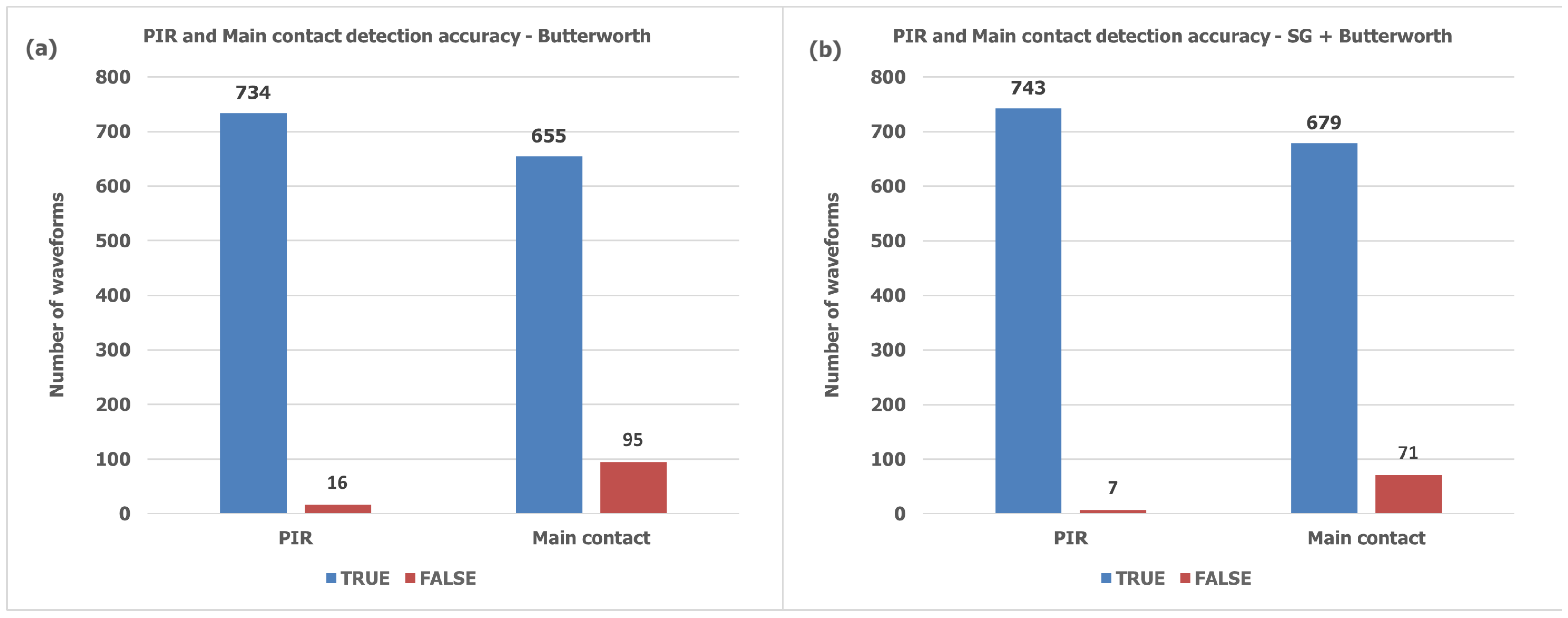
Figure 10 presents the accuracy results in detecting the PIR and main contacts.
The combination of Savitzky–Golay and Butterworth filters provides better accuracy for detecting circuit breaker contacts than the Butterworth filter alone, as demonstrated in
Figure 10, achieving an accuracy of 99.1% in detecting PIR contact (743 of 750 waveforms) and 90.5% for the main contact (679 of 750) in historical records of field measurements.
5.2. Case Study 2: Analysis of Real Field Record with Switching Optimization via Modeling and Simulation in ATP
In this second case study, a historical record of real field measurements from a Brazilian substation was chosen for analysis. The most important information about the switching process is represented in
Figure 11, including the maximum inrush current and the proposed adjustment for reparametrization of the switching controller. Note: Vref is the reference voltage used in the acquisition system of the Brazilian substation under study.
As presented in
Section 4.2 and
Section 4.3, the “PIR closing” instant was automatically detected using the proposed algorithm by identifying the first highest derivative peak, while the “Main closing” was determined via the second highest peak. The “Best point for main” occurs at the zero current crossing point prior to the moment of main contact closing. Finally, the proposed adjustment is calculated as the time difference between the points “Main closing” and “Best point for main”.
As can be seen in
Figure 11, a reparametrization (Adjustment) of 1.93 ms was proposed based on the analyses performed by the methodology. Since it was not possible to implement this adjustment in the field circuit breaker, the original switching condition from the real field record was modeled in ATP, representing the initial condition (before optimization), and the waveforms are shown in
Figure 12.
Both
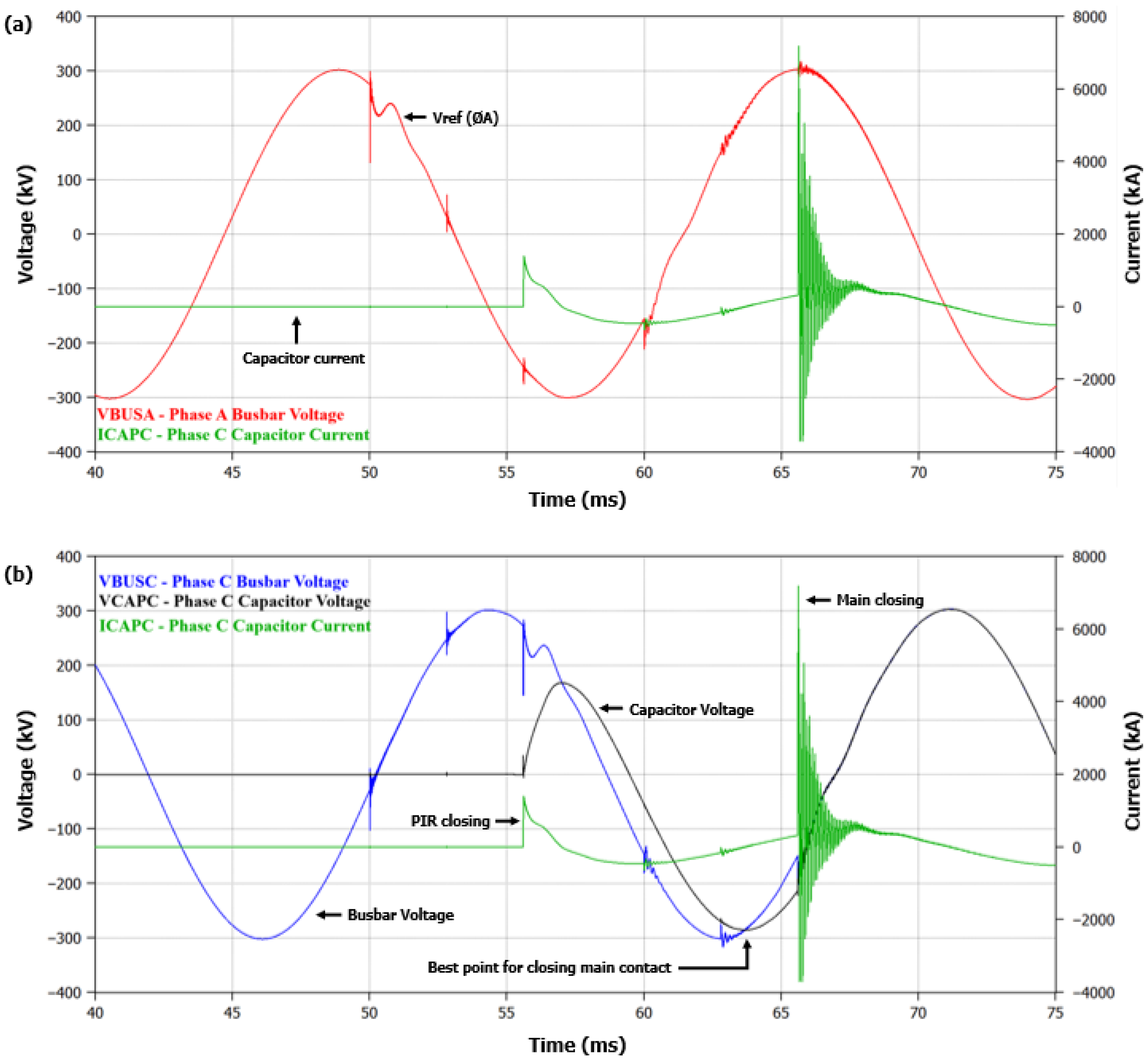
Figure 12a,b present the waveforms generated by the ATP simulation under the original switching condition extracted from the field record.
Figure 12a displays the same substation reference voltage (Phase A) and capacitor current waveforms to demonstrate their similarity with the field measurement plotted in
Figure 11, while
Figure 12b shows the relationship between the capacitor bank and busbar voltage for the studied phase (Phase C) to highlight the best point for inserting the main contact, marked by the point “Best point for closing main contact”, which occurs when the voltages of the capacitor bank and busbar are equal or very close.
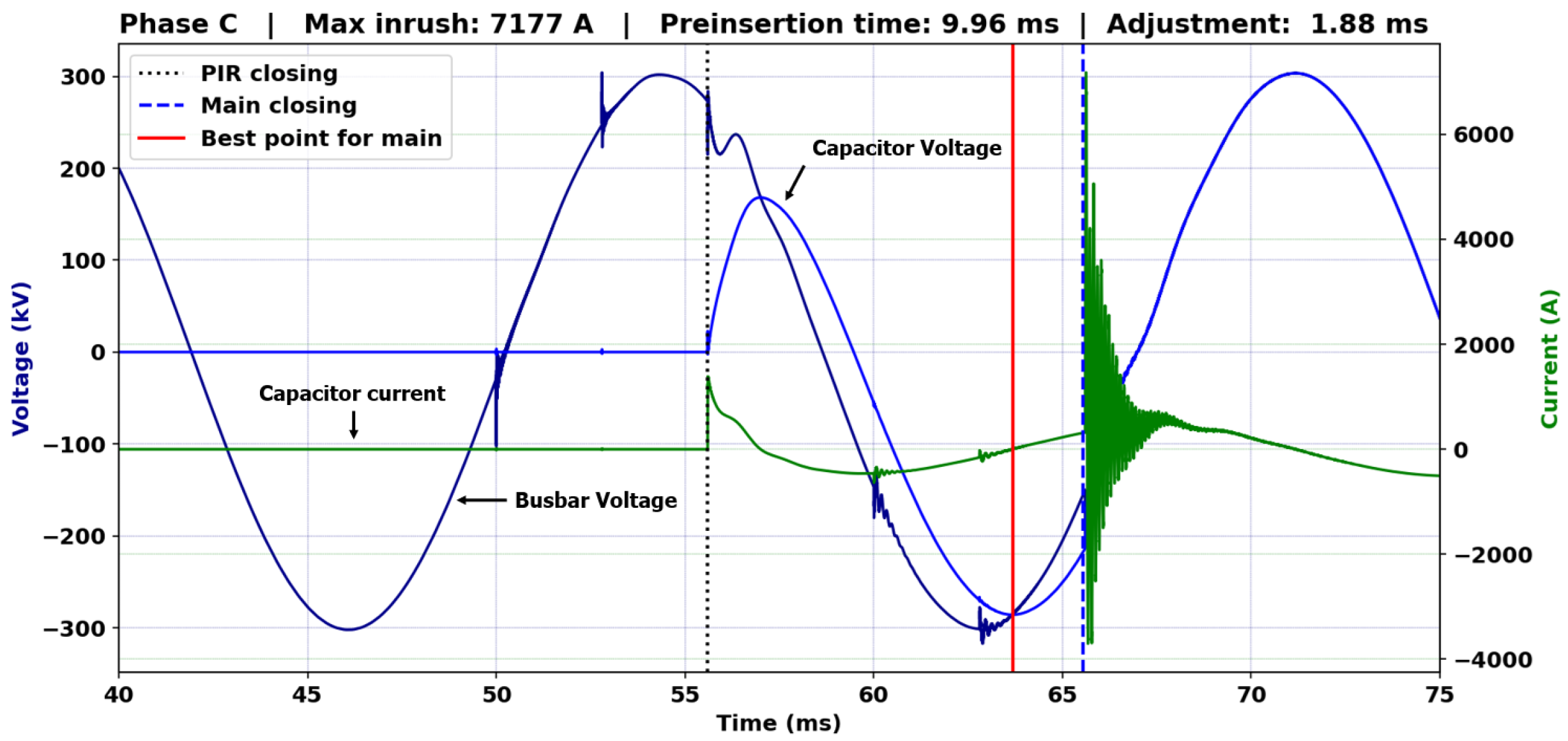
The COMTRADE file generated from the ATP simulation was processed and analyzed by the proposed computational tool. The results are demonstrated in
Figure 13.
Comparing the values of Max Inrush and Adjustment presented by
Figure 11 and
Figure 13, it is evident that the results obtained from simulation (
Figure 13) are very close to real field values (
Figure 11).
To optimize the switching process and reduce transient levels, the closing times of the “PIR” and “Main” switches (
Figure 9), which represent the contacts of the circuit breaker that closes the capacitor bank, were anticipated by 1.88 ms (Adjustment value shown in
Figure 13) to ensure the main contact closes at the optimal instant specified by the methodology.
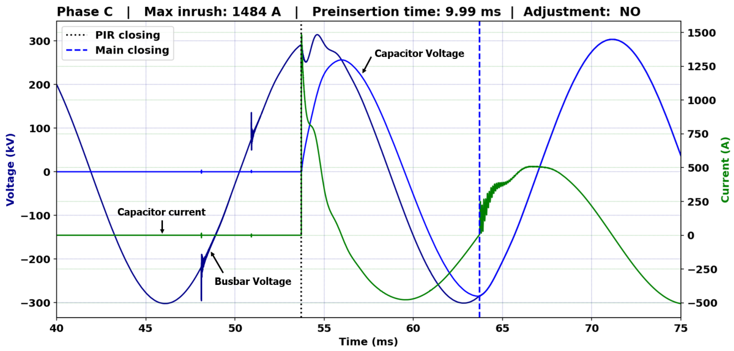
After running the simulation with the updated modeling parameters, a new file was generated, and the results are presented in
Figure 14.
Figure 14 proves that the adjustment proposed was effective in determining the ideal moment for closing the main contact, bringing very positive results in reducing the inrush current when compared to the values presented in
Figure 13; the adjustment also improved the waveforms, attenuating the transients generated during switching.
Table 1 shows a comparison between the current levels before and after optimization.
The results presented in
Table 1 show a reduction of 79% in the maximum inrush current for the ATP-simulated values of the real field record (from 7177 A to 1484 A) and a 96% reduction (from 7177 A to 250 A) for the main contact switching current after applying the proposed optimization (Adjustment).
5.3. Case Study 3: Reduction of Inrush Currents by Optimizing the Switching of a 345 kV Capacitor Bank by ATP Simulation
This study explores the energization of Capacitor Bank 03 (BC03—
Figure 3) under a severe closing condition, which occurs when the potential difference across the circuit breaker is high. Unlike Case Study 2, which analyzed real field data, in this case, ATP was used to generate such a condition, since no historical BC03 records with reparametrization values above 2.0 ms were found.
For the severe switching scenario to occur, the closing times of the “PIR” and “Main” (
Figure 9), which represent the contacts of the circuit breaker, were being adjusted until the simulation produced a high inrush current. Note: Capacitor Bank 02 (BC02—
Figure 3) was already closed before the energization of BC03, resulting in a back-to-back switching.
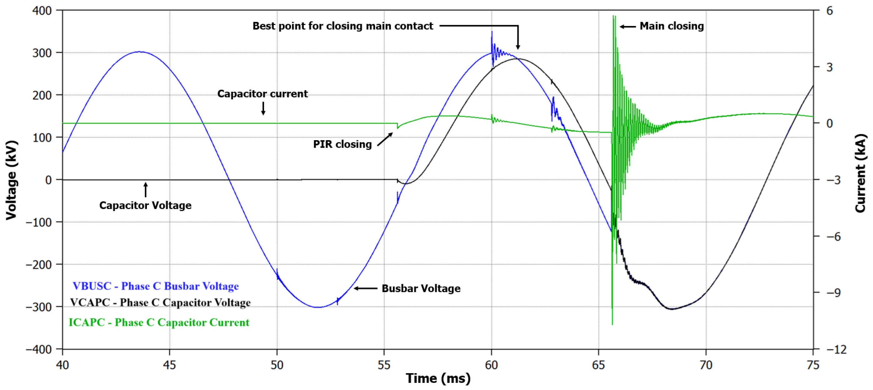
Figure 15 shows the waveforms from the simulation performed in a severe condition, which occurs when the main contact closes at a high potential difference between the busbar and capacitor bank voltages (point marked by the instant “Main closing”).
The file generated by ATP was analyzed using the methodology and the results are shown in
Figure 16.
The analysis of
Figure 16 reveals a high inrush current value (10,703 A) at the moment the main contact closes. This peak occurs due to the significant potential difference between the busbar and capacitor bank voltages. The solid vertical line (“Best point for main”) marks the optimal moment to insert the main contact of the circuit breaker, indicating a required adjustment of 4.32 ms (difference between the points “Main closing” and “Best point for main”).
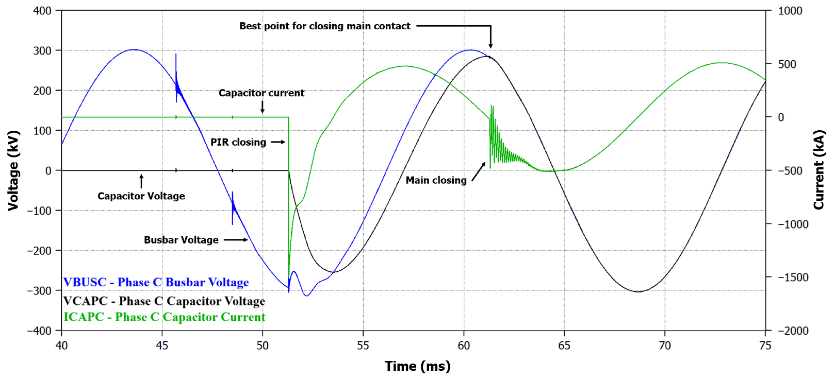
As a solution to reduce the inrush current and improve the waveforms, the proposed adjustment (4.32 ms) was performed by anticipating the closing times of the “PIR” and “Main” switches of the ATP modeling (
Figure 9). After running the simulation with the updated adjustment, a new file was generated, and the results are presented in
Figure 17 and
Figure 18. These figures illustrate the impact of the proposed methodology adjustment, showing a significant reduction in transient phenomena, with the inrush current reaching much lower values compared to the severe condition described at the beginning of this case study.
Figure 17 presents the waveforms generated in the ATP simulation, and
Figure 18 displays the methodology analysis based on the file generated.
A comparison between the switching current levels in the severe condition (initial—
Figure 16) and optimized (after carrying out the proposed adjustment—
Figure 18) can be seen in
Table 2.
The results presented in
Table 2 show a reduction of 86% in the maximum inrush current (from 10,703 to 1493 A), confirming the effectiveness of the proposed methodology in mitigating switching transients by indicating the best time for closing the main contact of the circuit breaker. Additionally, the main contact current was reduced by 96% (from 10,703 to 476 A), highlighting the effectiveness of the reparametrization.
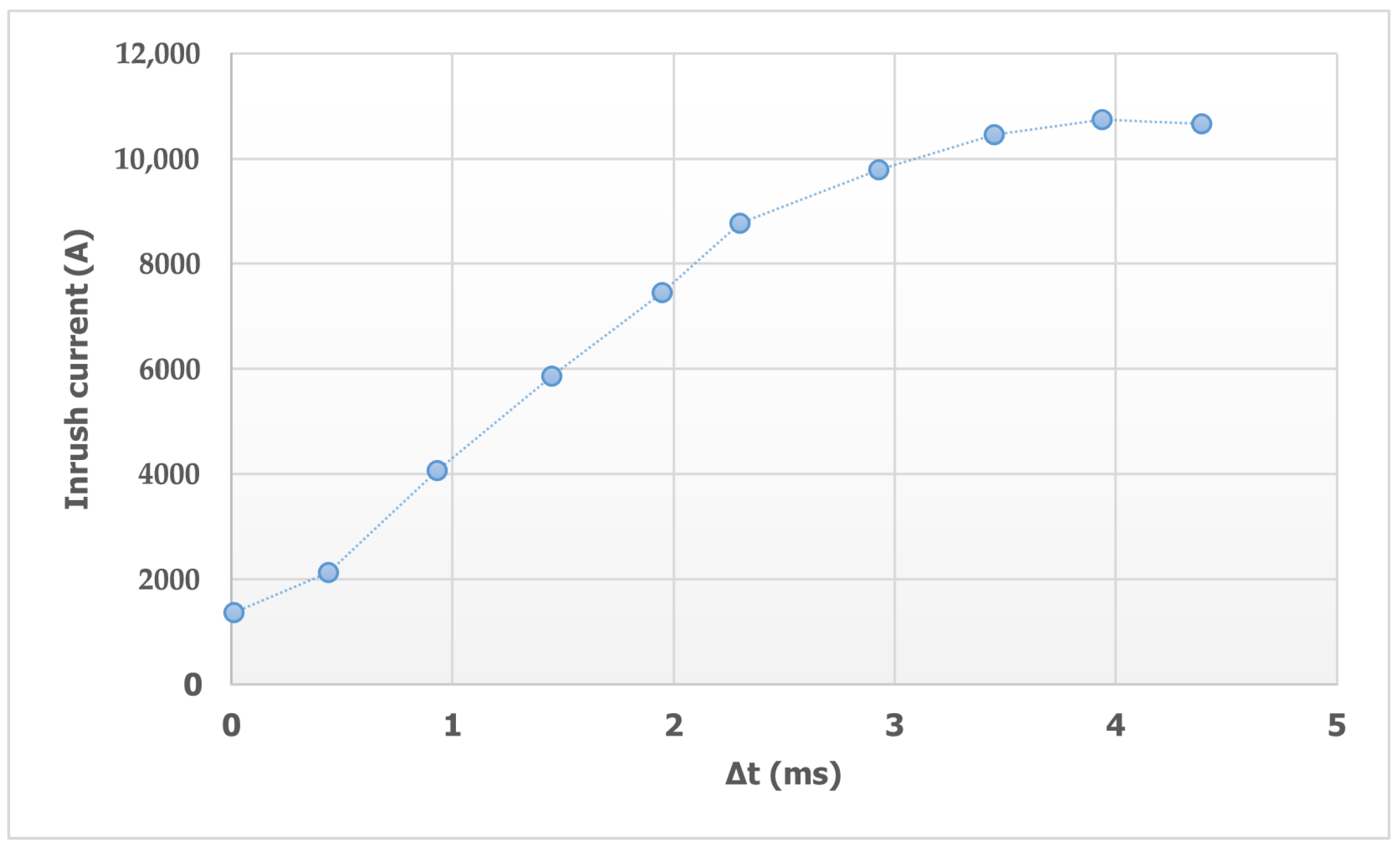
Extending the results obtained in Case Study 3,
Figure 19 illustrates the relationship between the magnitude of the inrush current and the proposed adjustment time (
) for the CSD.
6. Conclusions
This paper presented a new computational approach to optimize the controlled switching of capacitor banks operated by circuit breakers equipped with PIR. Through the analysis of real waveforms from historical files of a Brazilian 345 kV substation and simulated files generated by simulations in ATP, the methodology successfully identified the closing instants of the PIR and main contacts, allowing the calculation of the preinsertion time, the determination of the maximum inrush current, the determination of the best instant for the closing of the main contact, as well as the suggestion of the value for reparametrization. The combined use of Savitzky–Golay and Butterworth filters, with the application of the derivative on the filtered signal, guaranteed an efficiency in detecting resistive contacts of over 99% and main contacts of over 90% in 250 files (750 waveforms).
The results demonstrate a significant reduction in inrush current peaks, validating the effectiveness of the proposed solution both for single and back-to-back switching operations in HV systems.
Despite the positive results, the methodology has limitations in identifying the main contact input mainly in two situations: back-to-back switching where the closing of other phases causes high levels of transients in the form of current of the phase under study and in single switching with very smoothed current transients (closing very close to the optimum point).
Although the methodology demonstrates good results in offline analysis, several challenges arise when considering real-time implementation. The approach strongly relies on the accuracy of the sensors, since errors in current/voltage measurements (from CT/PT) can propagate through the derivative-based detection algorithm. Electromagnetic interference from adjacent switching operations can introduce noise that impairs signal quality.
The signal acquisition process—which comprises instrument transformers, analog-to-digital converters, and data transmission systems—can introduce inherent delays that can affect system responsiveness. These time constraints become particularly critical given the high sampling rates (100 kS/s) required for accurate transient detection and phase switching accuracy.
In addition, variations in network conditions (voltage, inductance, capacitance, and impedance levels) would require adaptive adjustments of filter parameters to maintain detection accuracy in different operating scenarios.
It is also important to emphasize that the strategy presented in this study can be extended to model other types of circuit breakers at different voltage levels. However, the current work focuses specifically on 345 kV circuit breakers, since the available historical data correspond to this voltage level.
Future work will focus on the integration of advanced signal processing techniques such as Fast Fourier Transform (FFT) and wavelets, along with AI techniques (machine learning, deep learning) to overcome these challenges and further increase the accuracy and reliability of the proposed solution.
Finally, this study provided a significant advance in the field of controlled switching applied to capacitor banks by reducing inrush current levels, as well as reducing transients during closing switching, through the automated proposal of the best parameterization values and ideal insertion points of the circuit breaker contacts.
Author Contributions
Conceptualization; methodology; software; validation; formal analysis; investigation: R.T.L. and A.L.M.C.; writing, review, and editing: R.T.L., A.L.M.C., G.B.V. and P.A.V.D.L.; resources; visualization; supervision; project administration, and funding acquisition: A.L.M.C. and G.B.V. All authors have read and agreed to the published version of the manuscript.
Funding
This research was funded by R&D Contract 8000012132, signed between Eletrobras and UNIFEI regarding the R&D project ANEEL PD-00394-2019/2021.
Data Availability Statement
Data are contained within the article.
Acknowledgments
The authors would like to thank the Coordination for the Improvement of Higher Education Personnel—Brazil (CAPES)—Financing Code 001, the National Council for Scientific and Technological Development (CNPQ), and the Federal University of Itajubá for their support. This research was funded by R&D Contract 8000012132, signed between Eletrobras and UNIFEI regarding the R&D project ANEEL PD-00394-2019/2021.
Conflicts of Interest
The authors declare that the research was conducted in the absence of any commercial or financial relationships that could be construed as a potential conflict of interest.
Abbreviations
The following abbreviations are used in this manuscript:
| AI | Artificial Intelligence |
| ATP | Alternative Transient Program |
| CIGRE | International Council on Large Electric Systems |
| COMTRADE | Common Format for Transient Data Exchange |
| CT | Current transformer |
| DRS | Dynamic Resistance Measurement |
| EPS | Electrical power systems |
| FFT | Fast Fourier Transform |
| IEEE | Institute of Electrical and Electronics Engineers |
| p.u. | Per unit |
| PIR | Preinsertion resistor |
| PT | Potential transformer |
| TRV | Transient Recovery Voltage |
References
- Sun, R.; McVey, M.; Yang, D.; Stage, J.R. A Study of Synchronous Breaker Switching With Preinsertion Resistor for Capacitors Banks. IEEE Trans. Power Deliv. 2018, 33, 821–829. [Google Scholar] [CrossRef]
- CIGRE WG A3.35. Guidelines and Best Practices for the Commissioning and Operation of Controlled Switching Projects; CIGRE: Paris, France, 2019. [Google Scholar]
- ABB. Power Capacitors and Harmonic Filters. Power Capacitors and Harmonic Filters–Buyer’s Guide; Technical Report; ABB: Ludvika, Sweden, 2013; Available online: https://studylib.net/doc/25222542/capacitors-buyers-guide-abb (accessed on 3 August 2025).
- Van Sickle, R.C.; Zaborszky, J. Capacitor Switching Phenomena. Trans. Am. Inst. Electr. Eng. 1951, 70, 151–159. [Google Scholar] [CrossRef]
- Funkhouser, A.W.; Van Sickle, R.C.; Shankle, D.F. Switching high-voltage shunt capacitor banks. Electr. Eng. 1951, 70, 596. [Google Scholar] [CrossRef]
- Van Sickle, R.C.; Zaborszky, J. Capacitor switching phenomena. Electr. Eng. 1952, 71, 126. [Google Scholar] [CrossRef]
- Patcharoen, T.; Ngaopitakkul, A. Combination of wavelet transforms and artificial intelligence in HV shunt capacitor banks: Fault and inrush currents classification. In Proceedings of the 15th International Conference on Developments in Power System Protection (DPSP 2020), Liverpool, UK, 10–12 March 2020; pp. 1–6. [Google Scholar] [CrossRef]
- Pothisarn, C.; Ngaopitakkul, A. Wavelet transform and artificial intelligence for unbalanced current protection of 230kV capacitor switching transient inrush current. In Proceedings of the 2021 IEEE/IAS 57th Industrial and Commercial Power Systems Technical Conference (I&CPS), Chengdu, China, 18–21 July 2021; pp. 1–7. [Google Scholar] [CrossRef]
- Liz, P.A.V.D.; Vitor, G.B.; Lima, R.T.; Coelho, A.L.M.; Silveira, E.P. AI-Driven Signal Processing for SF6 Circuit Breaker Performance Optimization. Energies 2025, 18, 377. [Google Scholar] [CrossRef]
- Michael Beanland, P.; Speas, T.; Joe Rostron, P. Pre-insertion resistors in high voltage capacitor bank switching. In Proceedings of the Western Protective Relay Conference, Spokane, WA, USA, 19–21 October 2004; pp. 1–12. Available online: https://www.caspoc.com/download/papers/TriAxis.pdf (accessed on 3 August 2025).
- IEEE Std 1036-2020 (Revision of IEEE Std 1036-2010); Guide for the Application of Shunt Power Capacitors. IEEE: New York, NY, USA, 2021; pp. 1–96. [CrossRef]
- IEEE Std 18-2012 (Revision of IEEE Std 18-2002); Standard for Shunt Power Capacitors. IEEE: New York, NY, USA, 2013; pp. 1–39. [CrossRef]
- Fantozzi, G.V. Selecting a capacitor switching overvoltage control method effective in preventing nuisance tripping of adjustable peed drives. In Proceedings of the EEI ES&E Committee Meeting, Clearwater Beach, FL, USA, 4 April 1995; pp. 1–2. [Google Scholar]
- Cowhey, E.; O’Donovan, M.; Connell, J. Performance and analysis of controlled switching on a transmission system. In Proceedings of the 2016 51st International Universities Power Engineering Conference (UPEC), Coimbra, Portugal, 6–9 September 2016; pp. 1–6. [Google Scholar] [CrossRef]
- IEEE Std C37.012-2022 (Revision of IEEE Std C37.012-2014); Guide for the Application of Capacitive Current Switching for AC High-Voltage Circuit Breakers Above 1000 V. IEEE: New York, NY, USA, 2023; pp. 1–90. [CrossRef]
- ABB. Technical Information—Guidelines for Selection of Surge Arresters for Shunt Capacitor Banks; ABB: Baden, Switzerland, 2001. [Google Scholar]
- Alexander, R.W. Synchronous Closing Control for Shunt Capacitors. IEEE Trans. Power Appar. Syst. 1985, PAS-104, 2619–2626. [Google Scholar] [CrossRef]
- Zondi, S.; Bokoro, P.; Paul, B. EMTP-based analysis of pre-insertion resistor and point on wave switching methodology. In Proceedings of the AFRICON 2015, Addis Ababa, Ethiopia, 14–17 September 2015; pp. 1–5. [Google Scholar] [CrossRef]
- Luz, G.S.; Arentz, D.S.; Junior, A.R.; Piantino, E.A.; Dias, J.B.; Braz, V.W.; Junior, A.D.P. Adjustment of switching controlled in the closing of the capacitor banks at the Tijuco Preto substation. In Proceedings of the XIII Eriac-Encontro Regional Iberoamericano Do CIGRÉ, Puerto Iguazú, Argentina, 24–28 May 2009. (In Portuguese). [Google Scholar]
- Zani, C.R.; Esmeraldo, P.C.V.; de Almeida, H.H.; Piantino, E.A.; Fernandez, P.C.; do Espírito Santo, S.; Feitosa, J.M.; Freitas, F.A.; Carvalho, F.M.S.; França, V.A.B.; et al. Energization Study of Large Capacitor Banks Carried out in a FURNAS Real-Time Digital Simulator (RTDS) Using Circuit Breakers with a Controlled Switching Device; Technical Report; FURNAS CENTRAIS ELETRICAS: Rio de Janeiro, Brazil, 1997. (In Portuguese) [Google Scholar]
- Luz, G.S.; Arentz, D.S.; Piantino, E.A. Investigation of the Influence of Capacitor Bank Operations on Autotransformer Failure in Tijuco Preto; Technical Report; FURNAS CENTRAIS ELETRICAS: Rio de Janeiro, Brazil, 2007. (In Portuguese) [Google Scholar]
- Brunke, J.H. Reduction of Capacitor Switching Transients by Controlled Closing. Master’s Thesis, Portland State University, Portland, OR, USA, 1980. Paper 3008. [Google Scholar] [CrossRef]
- de Souza, R.T.; da Costa, E.G.; de Oliveira, A.C.; de V. Sousa, W.; de Morais, T.C.M. Characterization of contacts degradation in circuit breakers through the dynamic contact resistance. In Proceedings of the 2014 IEEE PES Transmission & Distribution Conference and Exposition—Latin America (PES T&D-LA), Chicago, IL, USA, 14–17 April 2014; pp. 1–6. [Google Scholar] [CrossRef]
- AREVA. Introduction to Switching of Shunt Capacitor Banks; Technical Report; AREVA: Paris, France, 2007. [Google Scholar]
- Tsirekis, C.; Hatziargyriou, N. Control of shunt capacitors and shunt reactors energization transients. In Proceedings of the International Conference on Power Systems Transients (IPST), New Orleans, LA, USA, 28 September–2 October 2003; Available online: https://www.ipstconf.org/papers/Proc_IPST2003/03IPST04a-04.pdf (accessed on 3 August 2025).
- CIGRE Joint Working Group A2/C4.39. Electrical Transient Interaction Between Transformers and the Power System; Technical Report; CIGRE: Paris, France, 2014; Brochure 577A. [Google Scholar]
- IEEE Std C37.011-2019 (Revision of IEEE Std C37.011-2011); IEEE Guide for the Application of Transient Recovery Voltage for AC High-Voltage Circuit Breakers with Rated Maximum Voltage above 1000 V. IEEE: New York, NY, USA, 2019; pp. 1–127. [CrossRef]
- Patcharoen, T.; Ngaopitakkul, A.; Pothisarn, C. Inrush current analysis for switching large shunt capacitor bank in a 230 kV substation system. In Proceedings of the 2013 International Conference on Electrical Machines and Systems (ICEMS), Busan, Republic of Korea, 26–29 October 2013; pp. 1325–1329. [Google Scholar] [CrossRef]
- Jambukar, A.A.; Satarkar, M. Simulation analysis of switching of shunt capacitor bank in 220/22 kV substation. In Proceedings of the 2018 Second International Conference on Intelligent Computing and Control Systems (ICICCS), Madurai, India, 14–15 June 2018; pp. 1554–1559. [Google Scholar] [CrossRef]
- Goldsworthy, D.; Roseburg, T.; Tziouvaras, D.; Pope, J. Controlled switching of HVAC circuit breakers: Application examples and benefits. In Proceedings of the 2008 61st Annual Conference for Protective Relay Engineers, College Station, TX, USA, 1–3 April 2008; pp. 520–535. [Google Scholar] [CrossRef]
- IEEE Std C37.111-2013 (IEC 60255-24 Edition 2.0 2013-04); Measuring Relays and Protection Equipment—Part 24: Common Format for Transient Data Exchange (COMTRADE) for Power Systems. IEEE: New York, NY, USA, 2013; pp. 1–73. [CrossRef]
- Savitzky, A.; Golay, M.J.E. Smoothing and Differentiation of Data by Simplified Least Squares Procedures. Anal. Chem. 1964, 36, 1627–1639. [Google Scholar] [CrossRef]
- Shouran, M.; Elgamil, E. Design and Implementation of Butterworth Filter. Int. J. Innov. Res. Sci. Eng. Technol. (IJIRSET) 2020, 9, 7975–7983. [Google Scholar]
Figure 1.
Single-phase equivalent circuit for capacitor bank switching.
Figure 1.
Single-phase equivalent circuit for capacitor bank switching.
Figure 2.
Flowchart of the proposed methodology of this study.
Figure 2.
Flowchart of the proposed methodology of this study.
Figure 3.
200 Mvar 345 kV capacitor bank—BC03.
Figure 3.
200 Mvar 345 kV capacitor bank—BC03.
Figure 4.
Current and voltage waveforms acquired from a real power system.
Figure 4.
Current and voltage waveforms acquired from a real power system.
Figure 5.
Wrong main contact detection point. Dotted vertical line (···) marks the PIR closing instant and dashed line (- - -) shows main contact closing point.
Figure 5.
Wrong main contact detection point. Dotted vertical line (···) marks the PIR closing instant and dashed line (- - -) shows main contact closing point.
Figure 6.
Wrong PIR and main contact detection points. Dotted vertical line (···) marks the PIR closing instant and dashed line (- - -) shows main contact closing point.
Figure 6.
Wrong PIR and main contact detection points. Dotted vertical line (···) marks the PIR closing instant and dashed line (- - -) shows main contact closing point.
Figure 7.
Current signal processing steps: (a) original signal (raw current); (b) first filtering with Savitzky–Golay (window: 21 points, polynomial order: 3); (c) additional Butterworth filtering (order: 4, cutoff: 3 kHz); (d) gradient derivative .
Figure 7.
Current signal processing steps: (a) original signal (raw current); (b) first filtering with Savitzky–Golay (window: 21 points, polynomial order: 3); (c) additional Butterworth filtering (order: 4, cutoff: 3 kHz); (d) gradient derivative .
Figure 8.
Determination of the best point for closing the main contact. Dotted vertical line (···) marks the PIR closing instant, dashed line (- - -) shows main contact closing point, and solid line (—) identifies the best point to close the main contact of the circuit breaker.
Figure 8.
Determination of the best point for closing the main contact. Dotted vertical line (···) marks the PIR closing instant, dashed line (- - -) shows main contact closing point, and solid line (—) identifies the best point to close the main contact of the circuit breaker.
Figure 9.
ATP modeling of the capacitor bank BC03.
Figure 9.
ATP modeling of the capacitor bank BC03.
Figure 10.
Accuracy of detection of PIR and main contact closing instants: (a) results using only Butterworth filter for contact detection; (b) results using filters Savitzky–Golay combined with Butterworth (SG + Butter).
Figure 10.
Accuracy of detection of PIR and main contact closing instants: (a) results using only Butterworth filter for contact detection; (b) results using filters Savitzky–Golay combined with Butterworth (SG + Butter).
Figure 11.
Analysis of real field record waveforms. Dotted vertical line (···) marks the PIR closing instant, dashed line (- - -) shows main contact closing point, and solid line (—) identifies the best point to close the main contact of the circuit breaker. Note: All values and vertical lines (“PIR closing”, “Main closing”, and “Best point for main”) presented in
Figure 11 were determined automatically by the proposed algorithm.
Figure 12.
Simulated waveforms in ATP under real field conditions: (a) reference voltage versus capacitor current, (b) busbar and capacitor bank voltage versus current.
Figure 12.
Simulated waveforms in ATP under real field conditions: (a) reference voltage versus capacitor current, (b) busbar and capacitor bank voltage versus current.
Figure 13.
Analysis of real field data waveforms simulated in ATP before optimization. Dotted vertical line (···) marks the PIR closing instant, dashed line (- - -) shows main contact closing point, and solid line (—) identifies the best point to close the main contact of the circuit breaker.
Figure 13.
Analysis of real field data waveforms simulated in ATP before optimization. Dotted vertical line (···) marks the PIR closing instant, dashed line (- - -) shows main contact closing point, and solid line (—) identifies the best point to close the main contact of the circuit breaker.
Figure 14.
Results of real field file waveforms simulated in ATP after optimization. Dotted vertical line (···) marks the PIR closing instant and dashed line (- - -) identifies the closing point of the main contact of the circuit breaker. Note: All values and vertical lines (“PIR closing” and “Main closing”) presented in
Figure 14 were determined automatically by the proposed algorithm.
Figure 15.
Waveforms generated by simulation of capacitor bank 03 (BC03) in severe closing condition.
Figure 15.
Waveforms generated by simulation of capacitor bank 03 (BC03) in severe closing condition.
Figure 16.
Analysis of the simulation of capacitor bank 03 (BC03) switching in severe condition. Dotted vertical line (···) marks the PIR closing instant, dashed line (- - -) shows main contact closing point, and solid line (—) identifies the best point to close the main contact of the circuit breaker. Note: All values and vertical lines (“PIR closing”, “Main closing”, and “Best point for main”) presented in
Figure 16 were determined automatically by the proposed algorithm.
Figure 17.
Waveforms generated by simulation of capacitor bank 03 (BC03) after applying the proposed adjustment in a severe switching condition.
Figure 17.
Waveforms generated by simulation of capacitor bank 03 (BC03) after applying the proposed adjustment in a severe switching condition.
Figure 18.
Analysis of optimized switching of capacitor bank 03 (BC03) after applying the proposed adjustment in a severe switching condition. Dotted vertical line (···) marks the PIR closing instant, dashed line (- - -) shows main contact closing point, and solid line (—) identifies the best point to close the main contact of the circuit breaker. Note: All values and vertical lines (“Pir closing”, “Main closing”, and “Best point for main”) presented in
Figure 18 were determined automatically by the proposed algorithm.
Figure 19.
Inrush current versus (switching controller adjustment time)—results from BC03 simulations in ATP.
Figure 19.
Inrush current versus (switching controller adjustment time)—results from BC03 simulations in ATP.
Table 1.
Comparison of current levels before and after optimization—Case Study 2.
Table 1.
Comparison of current levels before and after optimization—Case Study 2.
| Condition | PIR Current | Main Contact Current | Max Inrush Current | Adjustment Time |
|---|
| Field measurements | 1151 A | 6573 A | 6573 A | 1.93 ms |
| ATP simulation (original) | 1384 A | 7177 A | 7177 A | 1.88 ms |
| ATP simulation (optimized) | 1484 A | 250 A | 1484 A | – |
Table 2.
Comparison of current levels before and after optimization—Case Study 3.
Table 2.
Comparison of current levels before and after optimization—Case Study 3.
| Condition | PIR | Main Contact | Max Inrush | Adjustment |
|---|
| Before optimization | 278 (A) | 10,703 (A) | 10,703 (A) | 4.32 ms |
| After optimization | 1493 (A) | 476 (A) | 1493 (A) | - |
| Disclaimer/Publisher’s Note: The statements, opinions and data contained in all publications are solely those of the individual author(s) and contributor(s) and not of MDPI and/or the editor(s). MDPI and/or the editor(s) disclaim responsibility for any injury to people or property resulting from any ideas, methods, instructions or products referred to in the content. |
© 2025 by the authors. Licensee MDPI, Basel, Switzerland. This article is an open access article distributed under the terms and conditions of the Creative Commons Attribution (CC BY) license (https://creativecommons.org/licenses/by/4.0/).
