Article

A Novel Two-Transformer Full-Bridge Converter with Integrated Boost Converter for Hold-Up Time Compensation

Department of Electrical Engineering, Inha University, Incheon 22212, Republic of Korea
*
Author to whom correspondence should be addressed.
Energies 2025, 18(16), 4268; https://doi.org/10.3390/en18164268
Submission received: 17 June 2025 / Revised: 6 August 2025 / Accepted: 7 August 2025 / Published: 11 August 2025
(This article belongs to the Special Issue Design and Control Strategies for Wide Input Range DC-DC Converters)

Abstract

This article presents a new full-bridge converter with two series-connected transformers (TTFB), designed to meet the hold-up time requirements in power systems. The conventional TTFB topology offers low root mean square (RMS) output current, clamped voltage stress across the primary switches, and zero-voltage switching (ZVS) capability. However, under a wide input voltage range, it suffers from a significant circulating current during the freewheeling period, leading to efficiency degradation. To mitigate this issue, a new converter is proposed by integrating the TTFB with a boost circuit, which operates during the hold-up state when the input voltage drops below the nominal level. Thus, the proposed converter can increase the duty ratio under nominal input voltage conditions, thereby reducing the primary-side RMS current and improving efficiency. To validate the effectiveness of the proposed method, a prototype with a 12 V/400 W output was implemented. The proposed converter achieved a peak efficiency of 92.1% at 50% load, and maintained a higher efficiency across the entire load range compared to the conventional design. Thus, the proposed converter offers a solution for applications demanding extended hold-up time with improved efficiency.

1. Introduction

Hold-up time refers to the duration during which a power converter must continue supplying a regulated output voltage after an alternating current (AC) input power interruption, as illustrated in Figure 1. This short-term backup capability is especially critical in modern power systems to ensure uninterrupted power delivery during brief outages. Applications such as telecom, data servers, industrial controllers, medical devices, and aerospace systems demand reliable operation, even during momentary input voltage sags or dropouts. In these systems, hold-up time serves as a key design parameter to avoid unintentional resets, data loss, or system malfunction.
To meet these application-specific hold-up time requirements, power converters must not only ensure reliable energy delivery during interruptions but also address size and cost constraints. During the hold-up time, i.e., when the AC line is momentarily lost, the energy required by the load is supplied by the DC/DC converter, which draws power from the bulky link capacitor. Therefore, the converter must be carefully sized to satisfy the requirements typically ranging from 10 ms to over 50 ms, depending on the relevant standards [1,2,3].
In practice, minimizing the size of the link capacitors is essential to reduce cost and improve the power density. One effective strategy is to employ converter topologies that maintain output voltage regulation over a wide input voltage range [4]. Among various converter topologies, the asymmetric half-bridge (AHB), phase-shifted full-bridge (PSFB), and LLC resonant converters are widely adopted due to their galvanic isolation and ZVS capability. However, these converters have several limitations when operating over a wide input voltage range. The asymmetric operation of the AHB converter induces a DC offset current in the transformer, which leads to uneven voltage stress on the rectifier diodes [5]. As a result, components with unbalanced voltage ratings are required, and the transformer size may need to be increased to avoid magnetic saturation [6]. The PSFB converter suffers from large circulating currents, which increase conduction losses. The LLC resonant converter requires a wide switching frequency range, leading to bulky magnetic components and an increased circulating current.
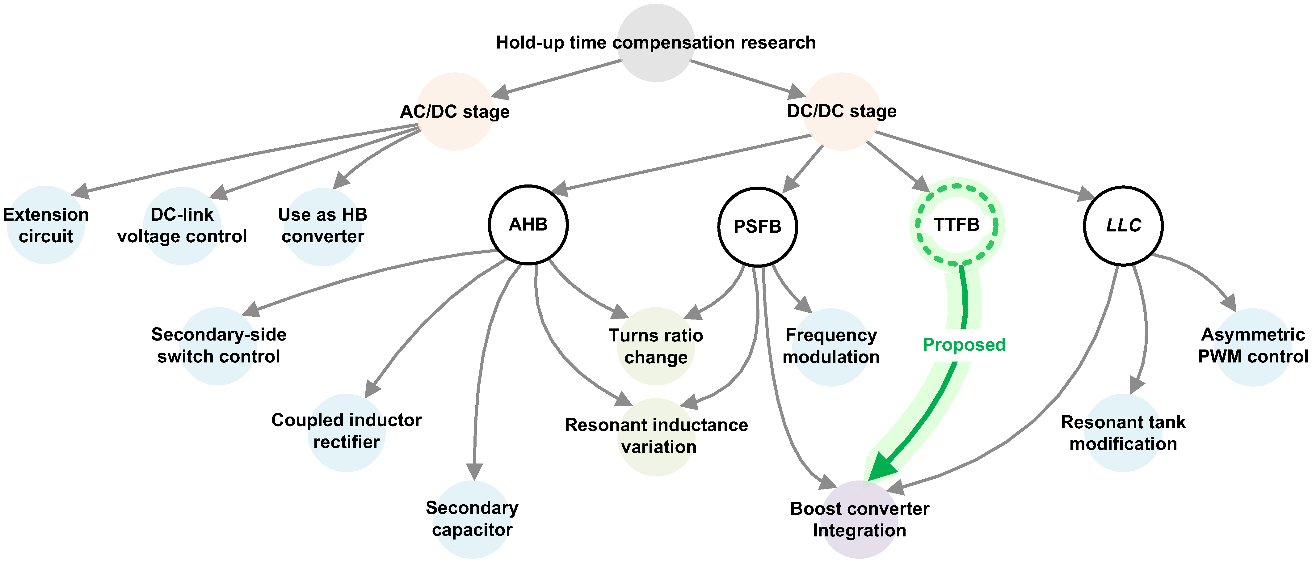
To solve these problems, researchers have proposed various hold-up time compensation techniques, as illustrated in Figure 2. The first approach involves improving AC/DC control strategies [7,8,9,10]. A method to compensate for the link capacitor voltage using an extension circuit was studied in [7,8]. However, the additional power diode in the main current path decreases the converter’s efficiency. A variable DC-link voltage control scheme is discussed in [9], and the use of a boost converter as a half-bridge converter is studied in [10]. However, placing a capacitor between the bridge diode and the AC/DC stage may lead to undesirable harmonic distortion.
The second approach focuses on optimization of the DC/DC stage. Various techniques have been studied to improve the inherent issues of each topology under wide input voltage conditions. In AHB converters, several techniques have been investigated to suppress the DC offset current [11,12,13,14,15]. Methods such as secondary side switch control, the use of a coupled inductor rectifier, and a secondary capacitor [11,12,13] have been shown to effectively reduce the DC offset current. These techniques allow for a symmetric duty ratio of the main and auxiliary switches. However, unbalanced voltage stress on the rectifier diodes may cause uneven switching losses, affecting system reliability. Other methods involve adjusting the transformer turns ratio to increase voltage gain [14,17]. Although these methods can be applied to other topologies, they require increased transformer winding turns and additional switching components. In PSFB converters, various techniques have been proposed to reduce circulating currents [16,17,18,19]. A frequency modulation scheme was employed to increase the voltage gain [16]. During the hold-up state, the operating frequency shifted to the lower side to increase voltage gain. However, the main transformer became bulky and lossy due to the design considerations for low-frequency operation. Additionally, the resonant inductance variation scheme [15,18] mitigates inherent defects of the topologies and provides voltage clamping for the rectifier diodes. However, the use of an additional inductor and two switches increases costs. Similarly, various approaches to limiting the switching frequency range in the LLC resonant converter have been proposed [20,21,22,23,24]. For example, an asymmetric pulse width modulation (PWM) control scheme [20] can achieve high voltage gain during the hold-up time, but the transformer remains bulky due to the transformer DC offset current. Resonant tank modifications [21,22,23] allow for voltage regulation within a narrow frequency range by varying the resonant capacitance or inductance. However, these methods typically require additional components, leading to higher costs.
Another candidate topology in DC/DC converter that does not require an output inductor is the full-bridge converter with two series-connected transformers (TTFB) [25], as shown in Figure 3a. These two transformers act not only as the main transformer but also as the output inductor [26,27]. The TTFB eliminates the need for an output inductor, simplifying the structure and manufacturing process [28,29]. In addition, the TTFB enables ZVS for all switches and extends the ZVS range for the lagging leg switches due to its increased leakage inductance. Furthermore, the control method is relatively simple, as it operates at a fixed switching frequency. The stress on the switching components is also balanced due to the symmetric operation of the primary switch legs. However, circulating current during the freewheeling interval remains a drawback [30]. Methods such as using a diode on the secondary side or adding a blocking capacitor on the primary side have been proposed to mitigate this issue [31,32]. Despite reducing circulating current, this issue remains and results in increased voltage stress on the rectifier diodes due to the voltage across the primary capacitor. An existing method [18], as shown in Figure 3b, can be applied to the TTFB for hold-up time compensation. This method clamps the voltage across the rectifier diodes while reducing circulating current. However, it requires high-voltage-rated switches and an auxiliary inductor.
This article proposes a new hold-up time compensation circuit for TTFB, as shown in Figure 4. By integrating a single MOSFET and auxiliary diodes on the secondary side, the proposed converter enables maximum duty ratio operation under nominal input voltage. This effectively eliminates circulating current and enables the use of low-voltage-rated rectifier diodes. Moreover, the additional components do not conduct during the nominal state. Therefore, the proposed method can prevent unnecessary losses from these components. Unlike similar techniques [19,24], the proposed converter supports a center-tap rectifier with fewer conducting components, enabling a simpler and more economical design.
To validate the advantages of the proposed converter, a prototype with an input range of 250–400 V and an output of 12 V/400 W is implemented, and both theoretical analysis and experimental results are presented.
The rest of this article is organized as follows. Section 2 presents the derivation and operational principle of the proposed converter. Section 3 provides the characteristics of the proposed converter. A 250–400 V input and 12 V/400 W output prototype was built and tested to verify the effectiveness and feasibility of the proposed converter in Section 4. Finally, Section 5 concludes this article.

2. Features of the Proposed Converter

2.1. Derivation of the Proposed Converter

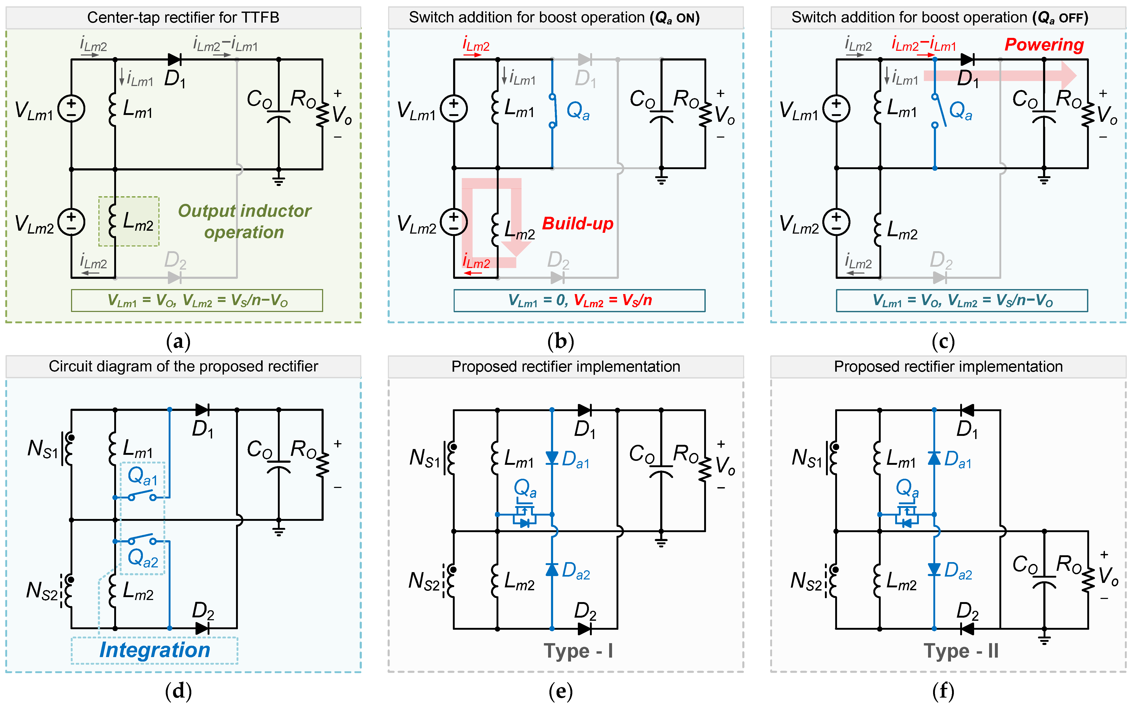
Figure 5 shows the derivation process of the proposed method for compensating the hold-up time. As shown in Figure 5a, the center-tap rectifier comprises two rectifier diodes (D1 and D2), an output capacitor (CO), and the magnetizing inductances (Lm1 and Lm2) of the transformers. In the conventional TTFB topology, when switches Q1 and Q4 are turned on, Lm2 operates as an output inductor. Figure 5b illustrates that, when the auxiliary switch Qa is added and turned on, diode D1 is turned off. Consequently, the voltage across Lm1 and Lm2 becomes zero and VS/n, respectively, where VS/n represents the input voltage reflected by the transformer turns ratio. As a result, the current through magnetizing inductance iLm1 remains constant, while the iLm2 increases, leading to the build-up mode. When Qa is turned off, as shown in Figure 5c, D1 turns on, and the current difference between iLm2 and iLm1 flows toward the output. This operation is referred to as the powering mode. Figure 5d shows the circuit for one full switching cycle operation, where auxiliary switches Qa1 and Qa2 can be merged into a single switch for simplification.
To realize this integration, auxiliary diodes Da1 and Da2 are required, as shown in Figure 5e, to prevent a short-circuit path through the transformers. Compared to the boost integration approach proposed in [33], the auxiliary components do not increase conduction losses during nominal operation, since the auxiliary diodes only conduct during the hold-up state. This feature significantly reduces conduction losses on the secondary side. Additionally, Figure 5f illustrates another type of rectifier configuration. The type II rectifier may be preferable, as it requires only one floating gate driver for Qa when synchronous rectifiers are used, compared to the type I rectifier.

2.2. Operational Principles

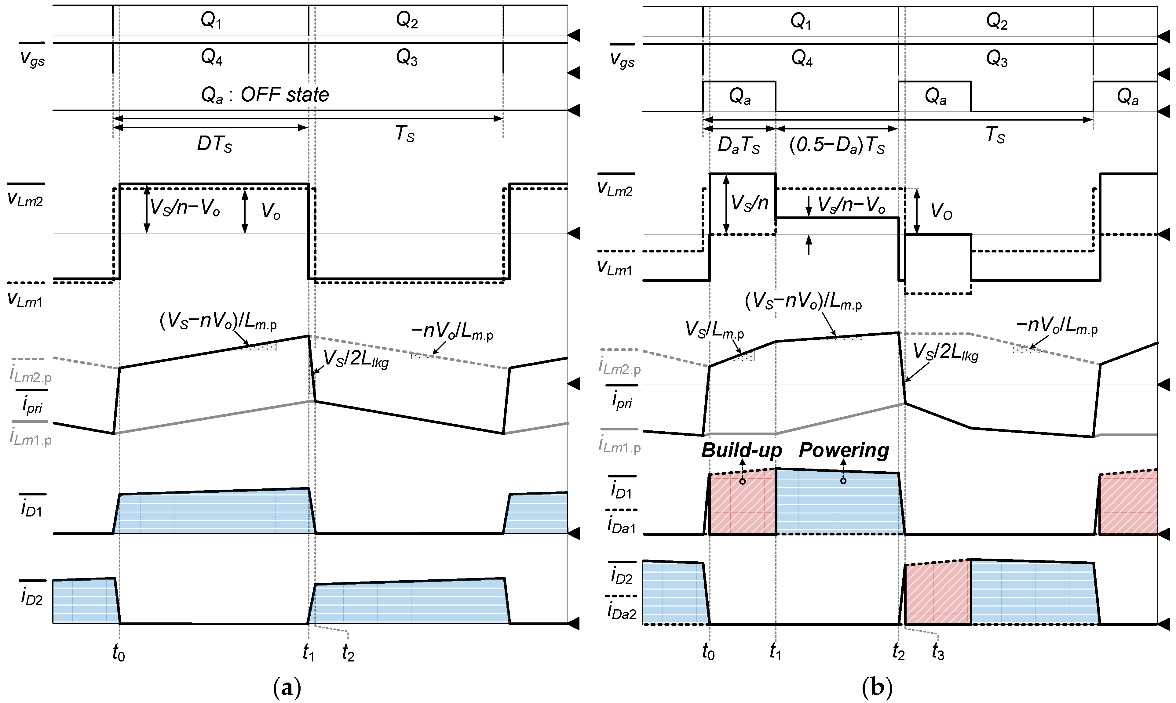
To explain the operational principles of the proposed converter, key waveforms and the equivalent circuits are presented in Figure 6, Figure 7 and Figure 8. The proposed converter operates in two main modes depending on the AC line status. The nominal state refers to the condition in which the auxiliary switch Qa remains off and the converter operates as a traditional TTFB, as shown in Figure 7. The hold-up state occurs when Qa is modulated using PWM to boost the output voltage, as shown in Figure 8. These two modes alternate according to input voltage conditions. The waveforms for the nominal state are shown in Figure 6a, while those for the hold-up state are presented in Figure 6b.
One switching cycle is divided into two half cycles. Since the two half cycles are symmetric except for the reversed current direction, only the first half cycle is explained. As shown in the key waveforms, Da denotes the duty ratio during which the switch Qa is turned on. For simplicity in the mode analysis, several assumptions are defined as follows:
(1)
The two transformers are identical, with the same turns ratio (Np1/Ns1 = Np2/Ns2 = n), magnetizing inductance (Lm1 = Lm2 = Lm), and leakage inductance (Llkg1 = Llkg2 = Llkg).
(2)
Magnetizing inductance Lm is sufficiently larger than leakage inductance Llkg (Lm >> Llkg).
(3)
The magnetizing inductances reflected to the primary side are denoted as Lm1.p and Lm2.p, and their values are equal to Lm.p.
(4)
Switches Q1Q4 operate ideally, except for output capacitance and body diode.
(5)
The additional switch Qa operates ideally, except for body diode.
(6)
The duty loss is neglected, and the output voltage is constant.

2.2.1. Mode Analysis: Nominal State Operation

In the nominal state, the proposed converter has the same circuit configuration as the conventional TTFB, as shown in Figure 3a, since the auxiliary switch Qa remains off. Its operating principle is identical to that of a conventional TTFB, which employs phase-shift modulation to control the primary switches. Since the proposed converter is designed to operate at the maximum duty ratio, the analyzed operating point is assumed to be D = 0.5.
Mode 1 [t0t1]: After Q1 and Q4 are turned on and the commutation of the secondary rectifier diodes D1 and D2 are completed, mode 1 starts. The transformer T1 acts as a forward type of transformer in this mode. Since iD1 and iD2 are commutated completely, D2 is turned off and D1 is still conducting. Therefore, Vo is applied across Lm1, and Vs/nVo is impressed on Lm2. That is, Lm2 plays a role as an inductor and determines the slope of the primary current in this mode. The energy stored in Lm2 during this mode should be discharged through D2 in all modes except for mode 1. The primary current ipri(t), magnetizing current iLm1.p(t), and current through D1 are determined as follows:
i p r i ( t ) = i p r i ( t 0 ) + V S n V O L m . p ( t t 0 )
i L m 1 , p ( t ) = i L m 1 , p ( t 0 ) + n V O L m . p ( t t 0 )
i D 1 ( t ) = i D 1 ( t 0 ) + n ( V S 2 n V O ) L m . p ( t t 0 ) .
Mode 2 [t1t2]: After Q1 and Q4 are turned off, the primary current flows back to the source through the output capacitor of Q2 and Q3. During this mode, the output capacitance of Q2 and Q3 start to be discharged, while those of Q1 and Q4 begin to be charged. Due to the energy stored in the leakage inductance, the current continues to flow through the body diodes of Q2 and Q3. Once the voltage across Q2 and Q3 drops to zero, ZVS turn-on is achieved. Meanwhile, when VLm2 reaches −Vo, the output current commutates from D1 to D2. This mode is essential for achieving soft switching. The ipri(t), iLm1.p(t), and iD1(t) are expressed as follows:
i p r i ( t ) = i p r i ( t 1 ) V S 2 L l k g ( t t 1 )
i L m 1 , p ( t ) = i L m 1 , p ( t 1 ) + n V O L m . p ( t t 1 )
i D 1 ( t ) = i D 1 ( t 1 ) n V S 2 L l k g + n V O L m . p ( t t 1 ) .

2.2.2. Mode Analysis: Hold-Up State Operation

Mode 1 [t0t1]: Mode 1 begins when switches Q1 and Q4 are turned on, and the auxiliary switch Qa is also turned on. Since the two transformers alternately act as a transformer and an output inductor during each half-cycle, transformer T1 (which includes Lm1) operates as the main transformer, while transformer T2 (which include Lm2) serves as the output inductor in this mode. Because Qa is turned on, zero voltage is applied to Lm1. Consequently, the input voltage Vs is applied to Lm2.p, which acts as the output inductor. As a result, the primary current increases with a slope of Vs/Lm.p. The ipri(t), iLm1.p(t), and iD1(t) are expressed as follows:
i p r i ( t ) = i p r i ( t 0 ) + V S L m . p ( t t 0 )
i L m 1 , p ( t ) = i L m 1 . p ( t 0 )
i D a 1 ( t ) = i D 1 ( t 0 ) + n V S L m . p ( t t 0 ) .
Mode 2 [t1t2]: Mode 2 starts when Qa is turned off. Since the output capacitance of Qa, i.e., Coss, is charged to the output voltage Vo, Da1 is turned off, and the rectifier diode D1 is turned on. As a result, the reflected voltage nVo is applied to Lm1,p, while the voltage across Lm2,p decreases to VsnVo. Therefore, ipri continues to increases, but with a lower slope of (VsnVo)/Lm.p. Meanwhile, the current difference iLm2iLm1 flows through diode D1 to the output. The ipri(t), iLm1.p(t), and iD1(t) are expressed as follows:
i p r i ( t ) = i p r i ( t 1 ) + V S n V O L m . p ( t t 1 )
i L m 1 , p ( t ) = i L m 1 , p ( t 1 ) + n V O L m . p ( t t 1 )
i D 1 ( t ) = i D a 1 ( t 1 ) + n ( V S 2 n V O ) L m . p ( t t 1 ) .
Mode 3 [t2t3]: Mode 3 begins when Q1 and Q4 are turned off. The output capacitance of Q2 and Q3 start to be discharged, while those of Q1 and Q4 begin to be charged. When VLm2 reaches −Vo, D2 conducts and the commutation between D1 and D2 is started. Since VLm1 is still maintained at Vo, the voltage across the leakage inductor V2Llkg is −Vs. As a result, ipri decreases with a slope of −Vs/2Llkg. The ipri(t), iLm1.p(t), iD1(t), and iD2(t) are expressed as follows:
i p r i ( t ) = i p r i ( t 2 ) V S 2 L l k g ( t t 2 )
i L m 1 , p ( t ) = i L m 1 , p ( t 2 ) + n V O L m . p ( t t 2 )
i D 1 ( t ) = i D 1 ( t 2 ) n V S 2 L l k g + n V O L m . p ( t t 2 )
i D 2 ( t ) = n V S 2 L l k g + n V O L m . p ( t t 2 ) .

3. Analysis of the Proposed Converter

3.1. Transformer Turns Ratio Design

The transformer turns ratio for a conventional converter is typically determined based on the minimum input voltage, with VS,min = 250 V selected to ensure proper output voltage regulation. In contrast, the proposed converter achieves increased voltage gain through secondary-side PWM control. Therefore, its transformer turns ratio can be designed based on the nominal input voltage, VS,nom.
In the prototype design, the mode transition is set to occur when the input voltage drops 5% below the nominal value (VS,nom = 400 V), i.e., at approximately VS,nom(min) ≈ 380 V. Considering a maximum effective duty ratio of Deff,max = 0.44, which includes both the dead time and commutation time within each switching cycle, the required conventional turns ratio nconv and proposed turns ratio nprop are calculated as follows:
n c o n v = V S , min D e f f , max V O
n p r o p = V S , n o m ( min ) D e f f , max V O
where Vo is the regulated output voltage. The resulting values of nconv and nprop are 9 and 14, respectively.

3.2. Voltage Gain Comparison

The normalized voltage gain of the proposed converter can be obtained by applying the volt-second balance to the magnetizing inductor. As shown in Figure 6a, the voltage applied to Lm2 in the nominal state is identical to that in the conventional TTFB converter. Consequently, the normalized voltage gain in the nominal state Mnom can be expressed as follows:
M n o m = n p r o p V O V S = D .
The voltage applied to Lm2 in the hold-up state is shown in Figure 6b. During the first half-cycle, the applied voltage is VS/n for Da·TS and (VS/nVo) for (0.5 − Da)TS. During the second half-cycle, the applied voltage is 0 for Da·TS and −Vo for (0.5 − Da)Ts. Therefore, the normalized voltage gain in the hold-up state Mhold can be expressed as follows:
M h o l d = n p r o p V O V S = 0.5 1 2 D a .
Figure 9 shows the graphs of the normalized voltage gain for the conventional and proposed converter as a function of duty ratio. Up to the maximum duty ratio, Dmax = 0.5, the normalized voltage gain is the same as that of the conventional converter. With the primary side duty ratio fixed at 0.5, an additional duty ratio is applied to Qa to further increase the voltage gain, as presented in Equation (20). Therefore, the proposed converter offers a higher voltage gain than the conventional design.

3.3. Circulating Current Comparison

Figure 10 shows the circulating current of the conventional and proposed converters. The circulating current of the proposed converter is lower than that of the conventional one. This results from the higher duty ratio of the primary-side switches. As a result, the freewheeling period is shortened, thereby further reducing the circulating current. The magnitude of the circulating current directly influences the primary-side RMS current. As the primary-side RMS current decreases, the corresponding power loss is also reduced.

3.4. ZVS Condition

The ZVS condition for the lagging leg switches is determined by the magnitude of the current at the switching instant and is expressed as follows:
E L a g _ l e g = 1 2 2 L l k g i p r i 2 ( t 1 ) 1 2 2 C o s s V S 2
i p r i ( t 1 ) = I O 2 n + V S n V O 2 L m . p D T S n V O L m . p ( 0.5 D ) T S .
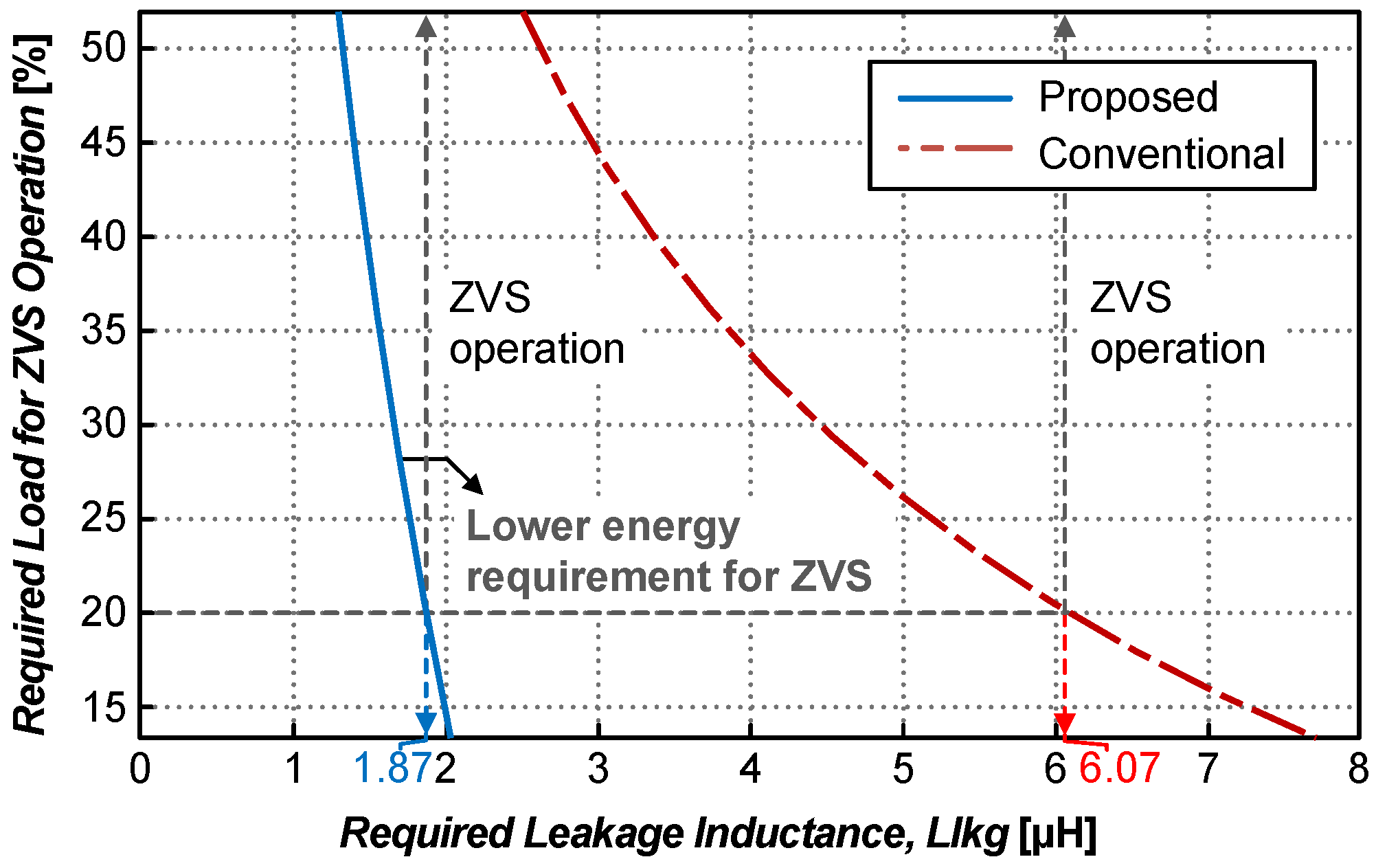
From (15) and (16), it is evident that the ZVS condition of the proposed converter is primarily determined by the leakage inductance and the load condition. Figure 11 illustrates the relationship between load and leakage inductance, assuming a constant duty ratio across the full load range. At 20% load, the leakage inductance required to achieve ZVS in the conventional converter is approximately 3.2 times that of the proposed converter. This indicates that the proposed converter requires less energy to achieve ZVS.

3.5. Voltage Stress on Rectifier Diodes

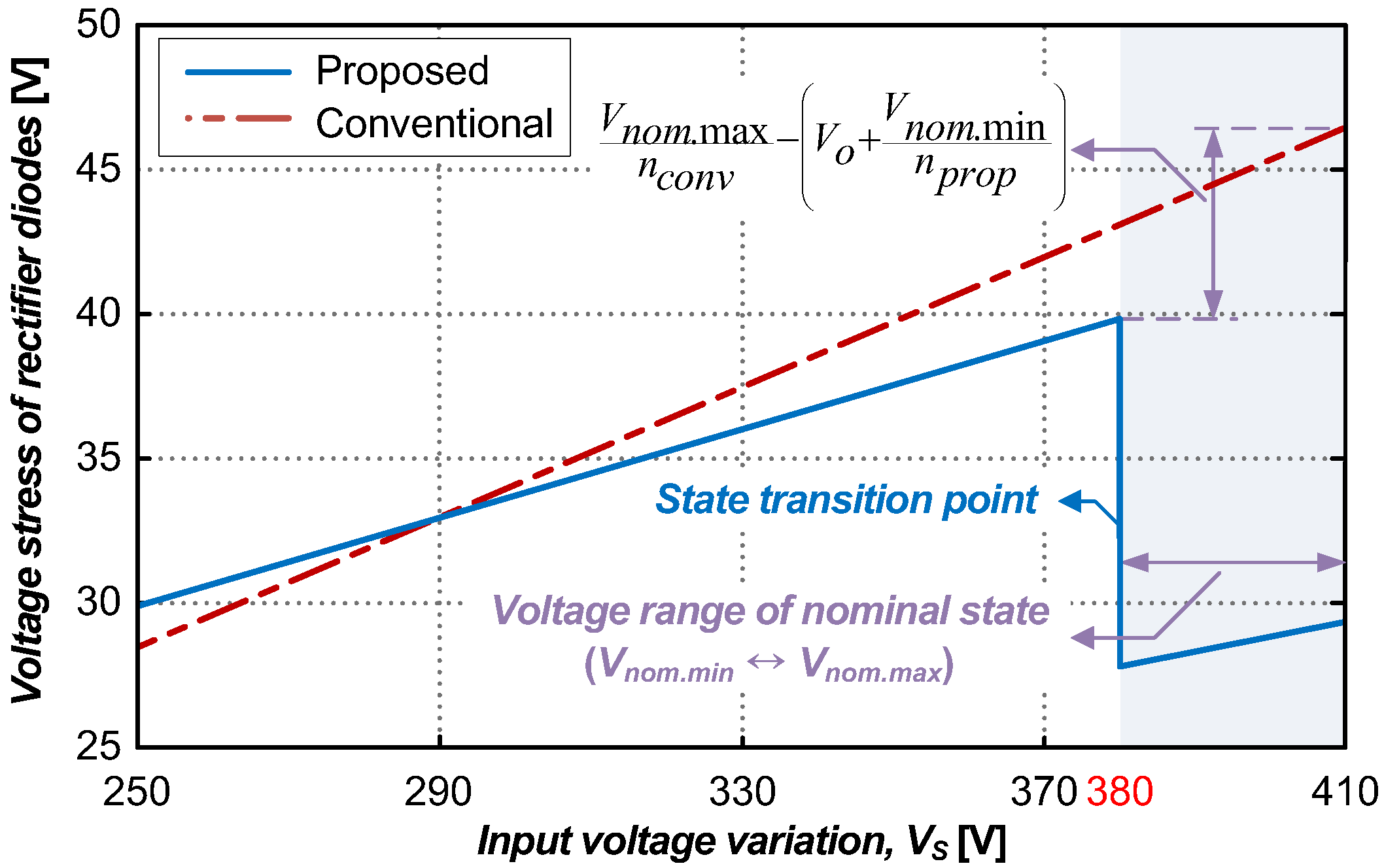
Figure 12 illustrates the voltage stress on the rectifier diodes of both the conventional and proposed converters. In the conventional converter, the voltage applied across rectifier diodes D1 and D2 is always VS/nconv in both the nominal and hold-up states, respectively.
The worst-case condition for the conventional converter occurs when the input voltage reaches its maximum during the nominal state. In the proposed converter, the voltage across D1 and D2 is VS/nprop, which is different only because of the transformer turns ratio. During the hold-up state, Vo + VS/nprop is applied to D1 and D2. Therefore, the maximum voltage stress occurs at the transition point between the nominal and hold-up states. Consequently, a voltage stress difference of 6.4 V is observed between the conventional and proposed converters. Considering a 150% design margin, diodes with a lower voltage rating were selected.

3.6. Conduction Losses in Power Devices

Power losses in semiconductor devices increase the junction temperature, which in turn degrades device performance. Minimizing these losses enhances thermal stability and improves system reliability.
  • Conduction losses in power MOSFETs:
The conduction losses for each MOSFET are given by the following:
P c o n d = I D r m s 2 × R D S ( o n )
where IDrms is the RMS value of the drain current, and RDS(on) is the drain source on-state resistance. All converters use identical MOSFETs; thus, RDS(on) is the same. Since the circulating current decreases in the order of conventional 1, conventional 2, and proposed, the proposed converter has the lowest IDrms, resulting in reduced conduction losses.
2.
Conduction losses in rectifier diodes:
In terms of reducing the number of conducting device, a center-tap rectifier employs two diodes, whereas a full-bridge rectifier requires four. Although the center-tap rectifier reduces the number of diodes by half, each experiences doubled voltage stress. This results in a higher forward voltage drop and increases conduction loss [34]. The loss for each diode is given by the following equation:
P d i o d e = V F × I D . a v g
where VF is the forward voltage of the diode, and ID,avg is the average current through the diode. The proposed converter allows the use of low-voltage-rated diodes in the rectifier circuit. Therefore, the proposed rectifier reduces the number of components and allows the use of diodes with low forward voltage drop, thereby lowering conduction losses.

3.7. Comparison with Previous Works

Table 1 presents a comparison between the proposed converter and previous works, highlighting the topological advantages and key contributions of this article. This subsection evaluates and compares various hold-up time compensation methods, based on the approaches discussed in Section 1, with a focus on the following key criteria:
  • Balanced rectifier stress: Unbalanced voltage stress on rectifier diodes requires components with different voltage ratings. The rectifier diodes in the proposed converter are balanced, enabling optimized component selection.
  • Output inductor reduction: An inductor is one of the most expensive and bulky components in a system. Eliminating it reduces system cost, improves power density, and simplifies circuit design. The proposed converter eliminates the output inductor, reducing the complexity while maintaining high performance.
  • Output current ripple: A larger peak-to-peak output current increases the current stress on the power semiconductor devices and imposes more stringent design requirements on the output capacitors. Since one transformer also functions as the output inductor, the proposed converter mitigates the output current ripple without requiring an additional inductor.
  • Additional components: To reduce the cost, the number of additional components should be minimized. The proposed converter introduces only three additional semiconductor devices.
  • Conducting components: To achieve high efficiency, the number of conducting devices should be minimized. As the proposed converter uses a center-tap rectifier, only one diode conducts during the nominal state.
  • Control complexity: A simplified control algorithm lowers hardware cost and reduces the time and effort required for design and verification. The proposed controller operates at a fixed switching frequency and applies PWM only to an auxiliary switch during the hold-up state, thereby maintaining a relatively low complexity.
  • Extended voltage gain range: Extending the voltage gain range preserves output regulation over a wide input range and allows optimal selection of design parameters—such as the transformer turns ratio and device ratings—to achieve high efficiency.

3.8. Link Capacitor Design

T H = η C L i n k ( V S , n o m 2 V S , min 2 ) 2 P O
C L i n k = 2 P O T H η ( V S , n o m 2 V S , min 2 ) .
The proposed converter is designed to maintain the output voltage for at least 20 ms during input loss. Based on Equation (26), the required capacitance is 205 μF under 400 V nominal input, 250 V minimum input, 400 W output power, and 80% efficiency. Accordingly, a 270 μF input capacitor is selected, exceeding the calculated value.

3.9. Comparision with Other Topologies

  • Power Loss Comparison
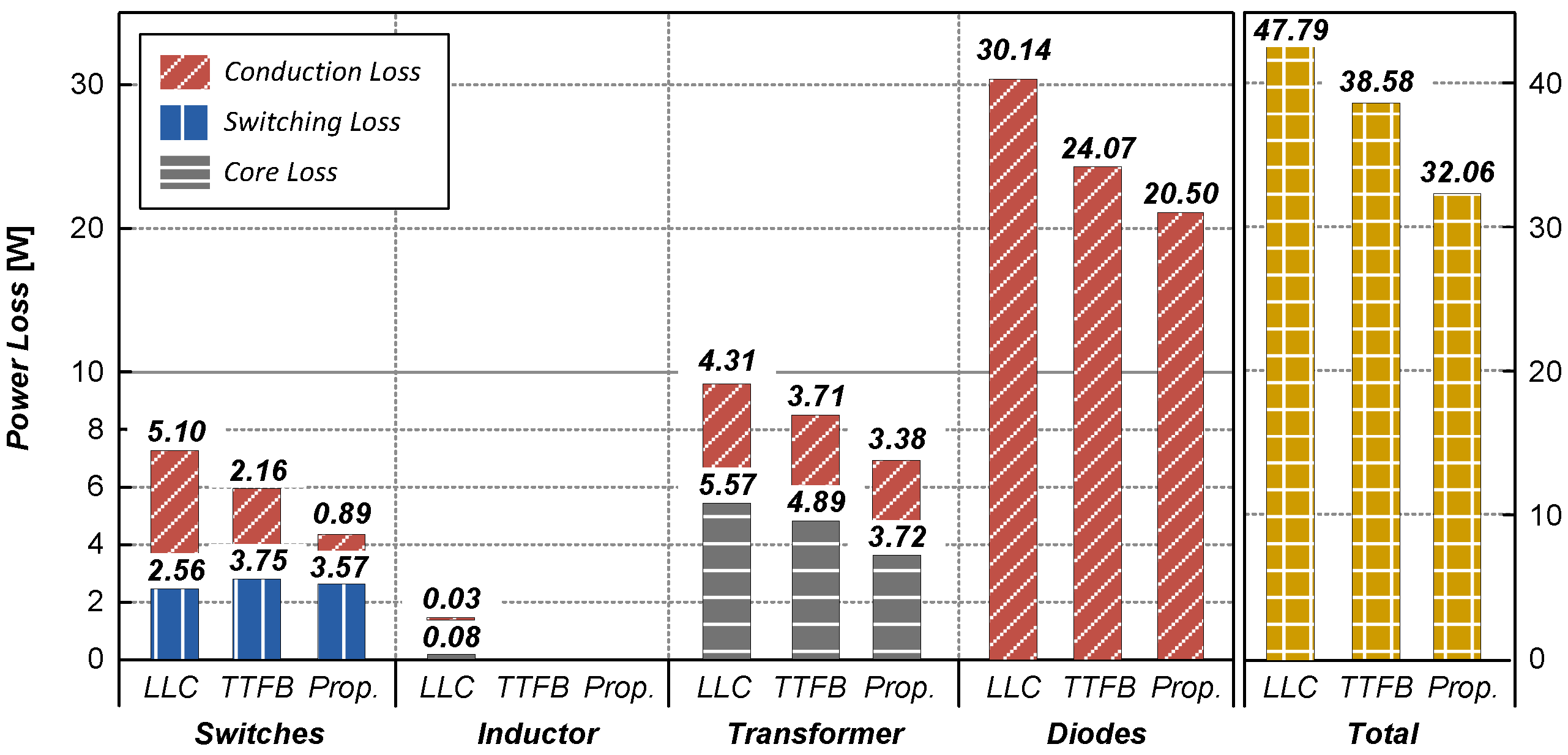
Figure 13 shows the power loss distribution of the LLC, TTFB, and proposed converters under nominal input voltage and full-load conditions. The LLC shows the highest loss of 47.79 W, mainly due to high diode losses. The TTFB reduces losses to 38.58 W with lower transformer and diodes losses. The proposed converter achieves the lowest total loss of 32.06 W by minimizing switch and diodes losses, demonstrating superior efficiency.
2.
Power Density Comparison
The power density was calculated based on the total volume of all components, including heat sinks. As shown in Table 2, the proposed converter achieves the highest power density, followed by the LLC and TTFB converters. This indicates that the proposed converter offers superior space efficiency.
3.
Cost Comparison
Table 3 presents the total cost for each converter. The TTFB converter has the lowest cost, while the proposed converter is the most expensive due to additional components. However, the improved performance and power density justify the higher cost.

4. Experimental Results

The effectiveness and feasibility of the proposed converter were verified under the following specifications: VS = 250–400 V, VS.nom = 400 V, Vo = 12 V, PO.max = 400 W, fsw = 70 kHz, and hold-up time TH = 20 ms. An experimental comparison was conducted among the conventional converter 1 [25], conventional converter 2 [18], and the proposed converter. Table 4 summarizes the components used in experiments. All transformer parameters were measured on the primary side.
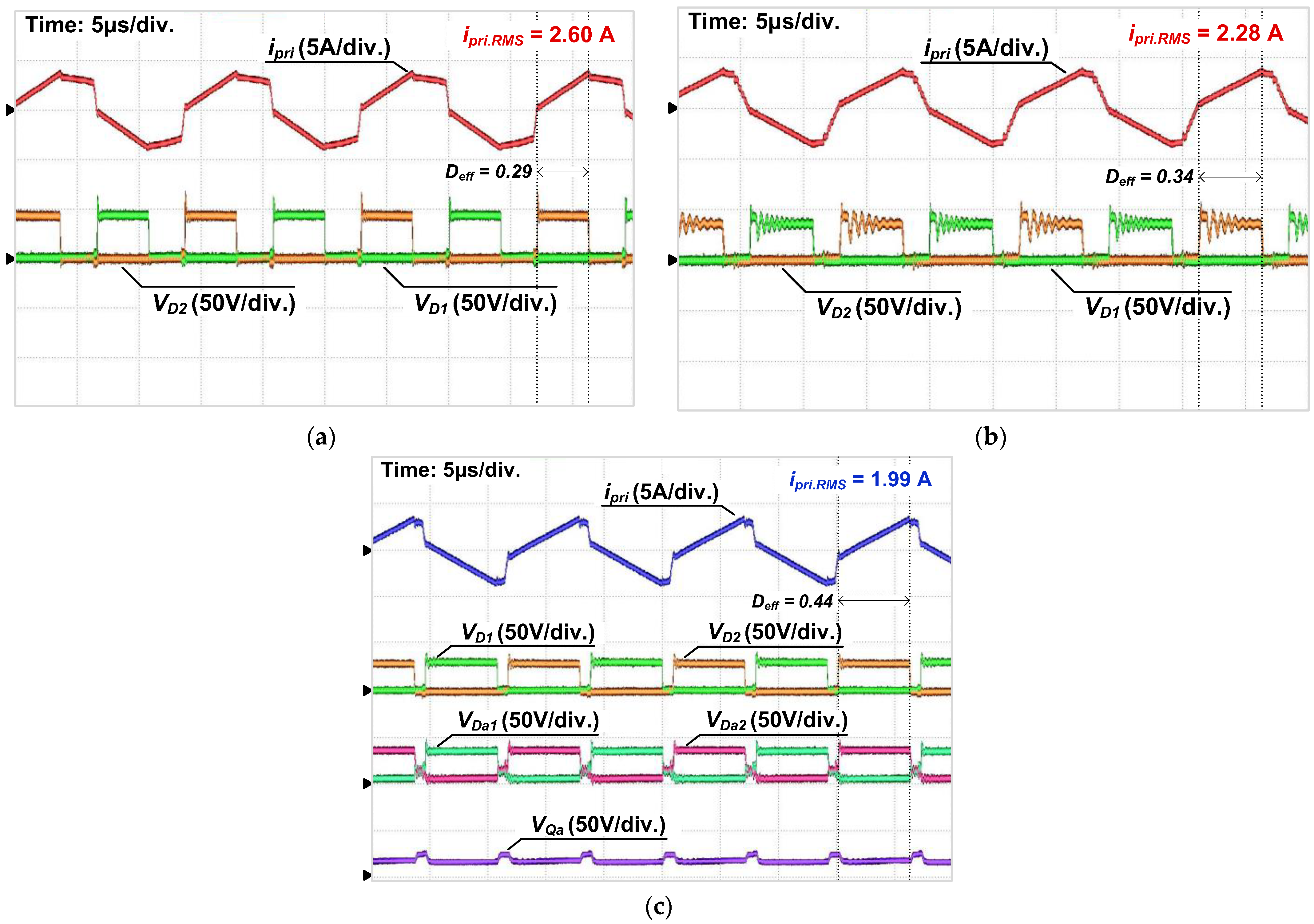
Figure 14 and Figure 15 show the key waveforms of the prototype converters under nominal and hold-up states at full load conditions, respectively. As shown in Figure 14a, conventional converter 1 operates with a small duty ratio at a nominal input voltage of 400 V, resulting in a high RMS current. In conventional converter 2, the circulating current is reduced by utilizing inductor La, as shown in Figure 14b. However, voltage ringing is observed at the rectifier diodes due to the resonance between inductor La and the parasitic capacitors of switches Q5 and Q6. In contrast, the proposed converter minimizes primary-side RMS current by operating at the maximum duty ratio, as shown in Figure 14c. Additionally, rectifier diodes D1 and D2 experience reduced voltage stress, allowing the use of low-voltage-rated diodes. During the nominal state, the secondary-side switch Qa remains off, and current flows only through D1 and D2.
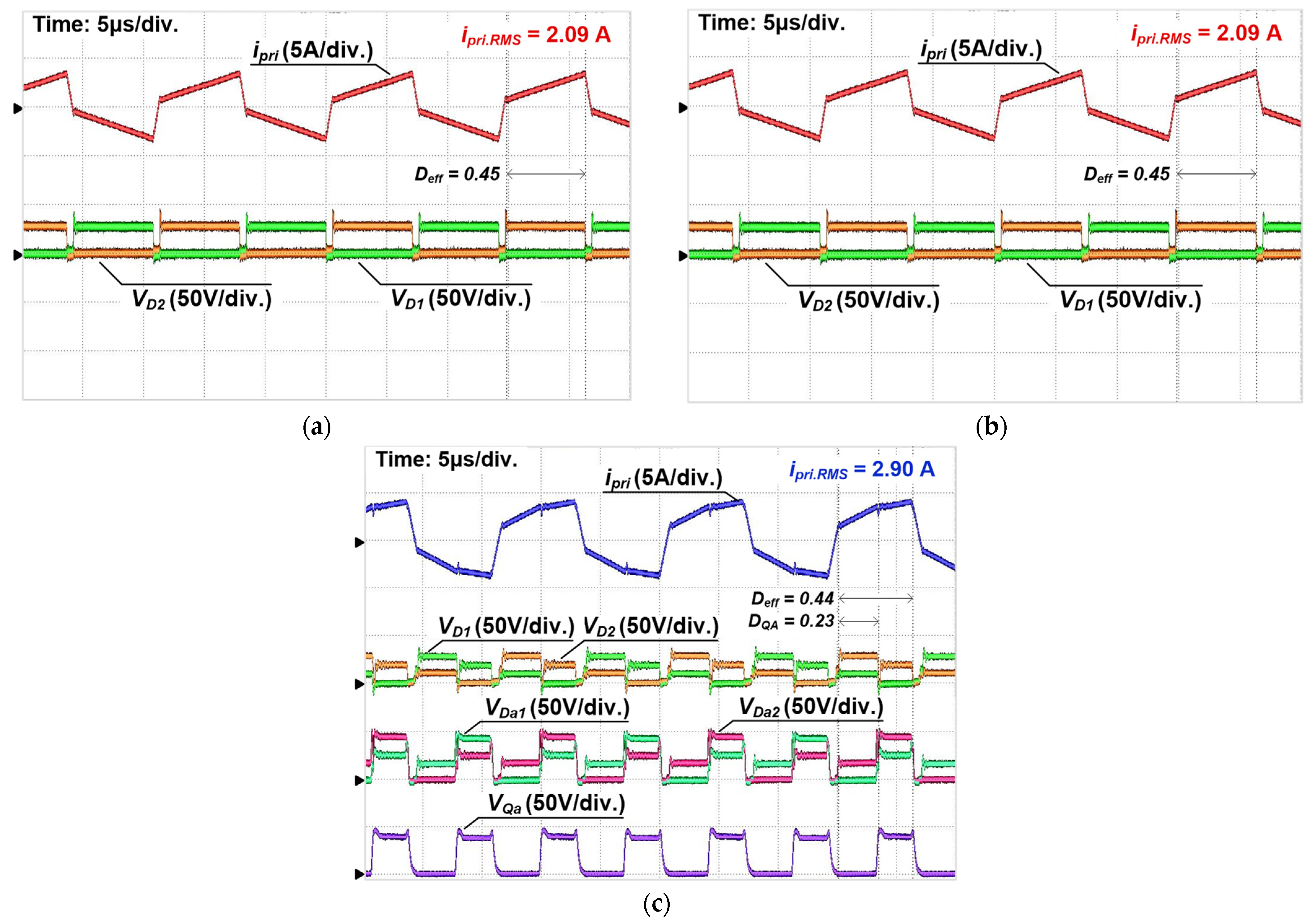
Figure 15a shows the waveform of conventional converter 1 at the minimum input voltage. The duty ratio of the primary-side switches reaches its maximum value of 0.5, and the voltage across the rectifier diodes decreases accordingly. In conventional 2, during the hold-up state, switches Q1 and Q2 are kept off, while switches Q3 to Q6 operate, effectively performing the same function as conventional converter 1 during the hold-up state, as shown in Figure 15b. In the proposed converter, as shown in Figure 15c, the auxiliary switch Qa operates during the hold-up state, resulting in increased voltage gain. During the operation when Q1 and Q4 are on, auxiliary diode Da1 conducts together with Qa when Qa is turned on. When Qa is turned off, Da1 also turns off, and power is delivered to the output through D1. Similarly, during the opposite half-cycle when Q2 and Q3 are on, Da2 conducts with Qa when Qa is turned on, and turns off when Qa is turned off, allowing power transfer through D2.
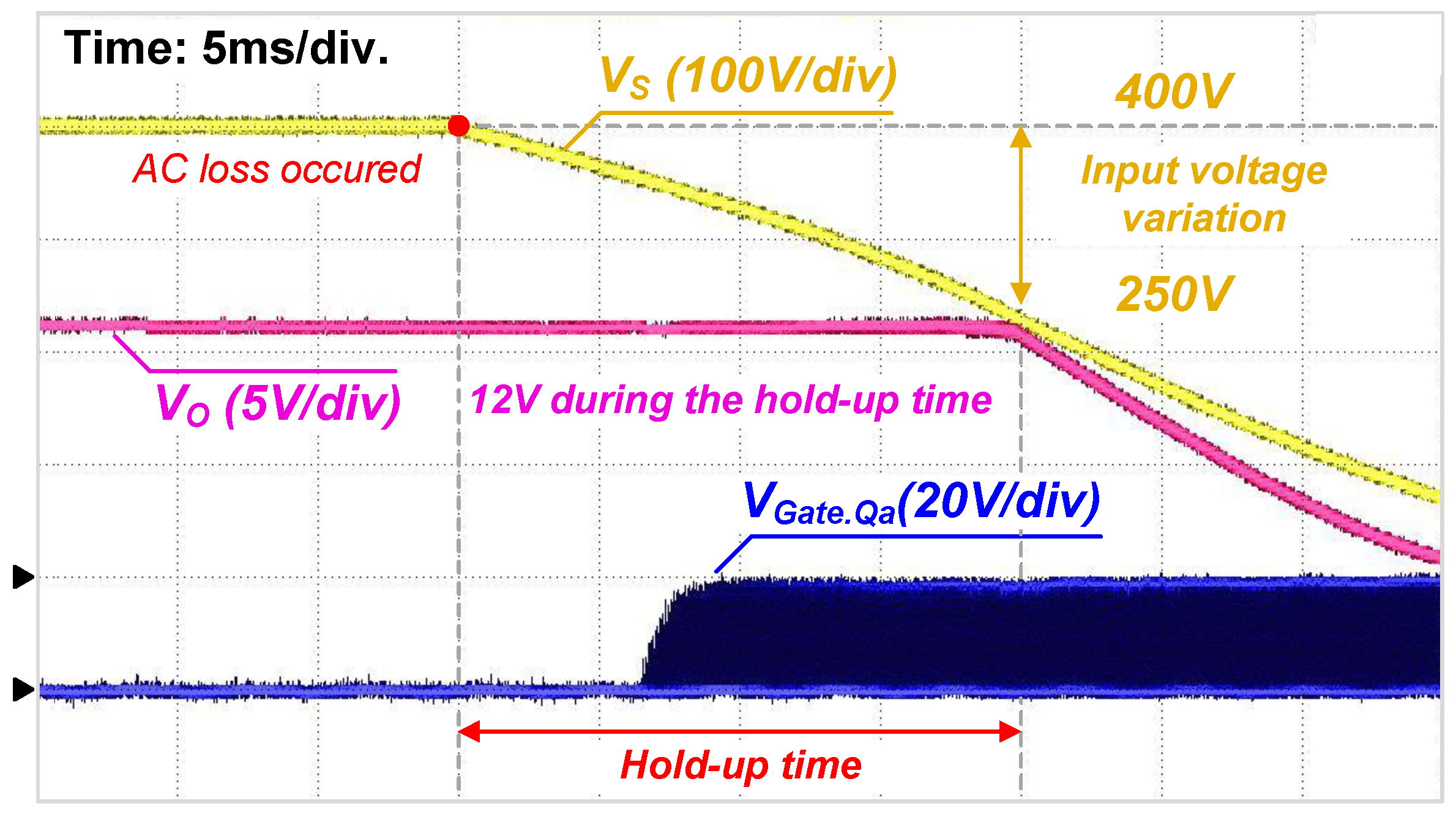
Figure 16 presents the waveforms of the transient operation during the hold-up time. When AC loss occurs, the input voltage VS begins to drop gradually. As the input continues to fall, the duty D increases and eventually reaches 0.5. After this point, the auxiliary switch Qa is turned on to maintain a stable output voltage. Consequently, the output voltage is tightly regulated during the hold-up time.
Figure 17 presents the thermal image of the proposed converter under a full load condition with the minimum input voltage. As shown in Figure 17a, the secondary side exhibits a higher temperature than the primary side due to significant output current. In particular, as illustrated in Figure 17b, the auxiliary switch shows the highest temperature among the secondary-side components. This measurement was taken over a period longer than the actual hold-up time. Approximately 40 °C of heat is measured at the rectifier diodes, auxiliary diodes, and the transformers.
To ensure a fair and consistent evaluation, the performances of both the conventional and proposed converters were measured using the same experimental setup. The KEYSIGHT N8950A (Keysight Technologies, Santa Rosa, CA, USA) was employed as the input DC power supply, and the CHROMA 63204A (Chroma ATE Inc., Taoyuan, Taiwan) was used as the programmable output load. A YOKOGAWA WT1800 (Yokogawa Electric Corporation, Tokyo, Japan) power analyzer was used for power measurement, and waveform observation was conducted using a YOKOGAWA DLM2024 (Yokogawa Electric Corporation, Tokyo, Japan) oscilloscope with a 701929 current probe and 701978 differential probes. Digital control was implemented using a TMS320F28069M (Texas Instruments, Dallas, TX, USA) microcontroller, and AGILENT E3648A (Agilent Technologies, Santa Clara, CA, USA) provided the auxiliary low-voltage power supply.
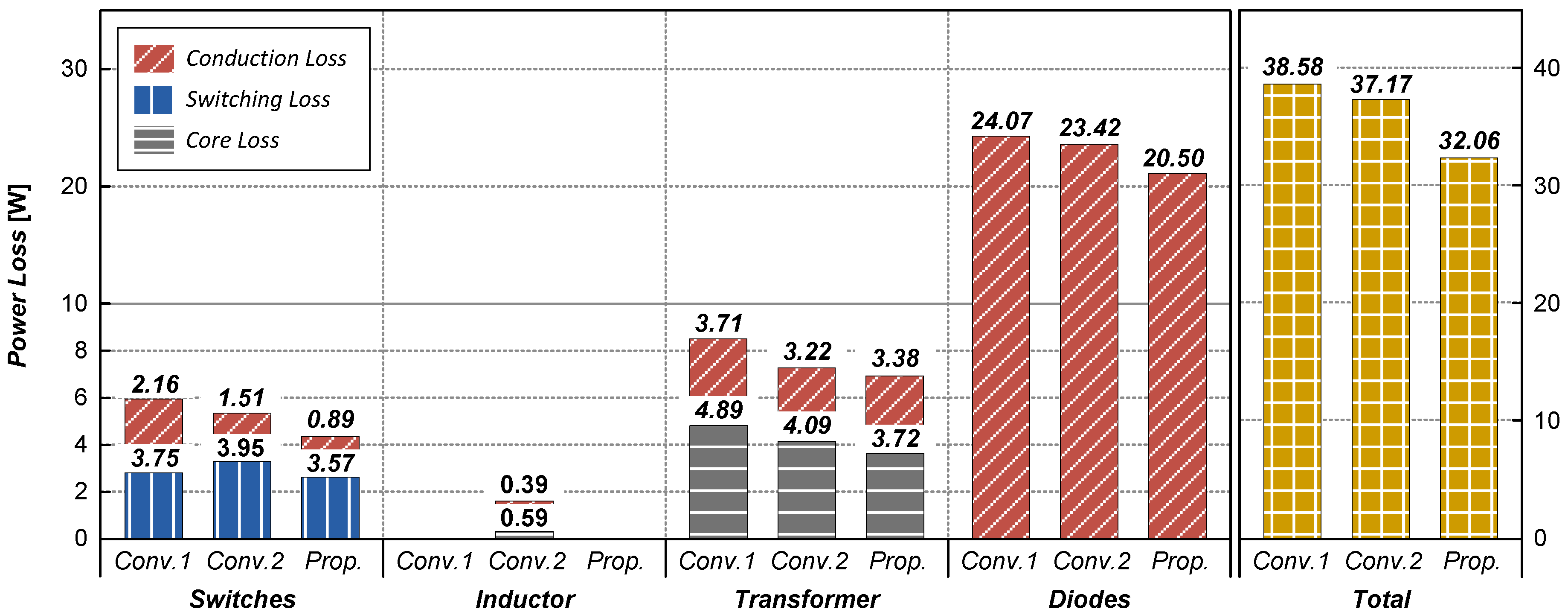
Figure 18 presents a detailed comparison of the power losses in the main components of the three converter configurations under nominal input voltage and full load condition. To ensure a fair comparison, the converter in [18] was reconfigured with two series-connected transformers to match the structure of the proposed topology. Compared to the conventional converters, the proposed converter exhibits the lowest conduction loss in the primary-side switches due to a reduced circulating current. This is because, as the circulating current decreases, the drain-source RMS current flowing through the switches also reduces, effectively lowering the conduction loss in the proposed converter. In addition, the proposed transformer has a greater number of primary turns, which lowers flux density variation and thus reduces core loss. Furthermore, secondary-side conduction loss is also minimized by adopting low-voltage-rated diodes. As a result, the total power loss in the proposed converter is reduced by 6.5 W and 5.1 W compared to conventional converter 1 and 2, respectively.
Figure 19 shows the measured efficiency curves under nominal input condition. Although the proposed converter includes an additional MOSFET and two auxiliary diodes, these components do not conduct during the nominal state and, therefore, do not contribute to additional losses. Consequently, the proposed converter achieves higher efficiency than both conventional converters across the entire load range.

5. Conclusions

In this article, a new TTFB converter with a center-tap rectifier structure is proposed. Although conventional converters can be designed to operate at lower input voltages to ensure sufficient hold-up time compensation, this approach results in significant primary-side circulating current in the nominal state. The proposed converter integrates a boost stage with a single MOSFET and two auxiliary diodes, enabling operation at maximum duty ratio in the nominal state. As a result, the circulating current is effectively eliminated. Furthermore, by adopting a higher transformer turns ratio, the proposed converter enables the use of low-voltage-rated diodes. As a result, both primary- and secondary-side losses are significantly reduced. Moreover, as no additional losses are incurred in the nominal state, high efficiency is achieved. Furthermore, the proposed converter eliminates the need for an output inductor and maintains ZVS with a significantly lower leakage inductance. Experimental results confirmed peak efficiencies of 92.1% at 50% load under nominal conditions. It consistently outperforms traditional TTFB converters across the entire load range. Consequently, the proposed converter is a promising candidate for hold-up time applications requiring high efficiency.

Author Contributions

Conceptualization, B.-S.L. and J.-K.K.; validation B.-S.L. and Y.-A.K.; writing—original draft, B.-S.L.; writing—review and editing, B.-S.L. and Y.-A.K.; visualization B.-S.L.; supervision, J.-K.K. All authors have read and agreed to the published version of the manuscript.

Funding

This research received no external funding.

Data Availability Statement

The original contributions presented in this study are included in the article. Further inquiries can be directed to the corresponding author.

Conflicts of Interest

The authors declare no conflicts of interest.

References

  1. EN 50155; Railway Applications—Rolling Stock—Electronic Equipment. European Committee for Electrotechnical Standardization (CENELEC): Brussels, Belgium, 2021.
  2. IEC 62040-3 Ed 3.0; Uninterruptible Power Systems (UPS)—Part 3: Method of Specifying the Performance and Test Requirements. International Electrotechnical Commission: Geneva, Switzerland, 2021.
  3. MIL-STD-704E; Aircraft Electric Power Characteristics. Department of Defense: Arlington, VA, USA, 1991.
  4. Wang, X.; Tian, F.; Batarseh, I. High efficiency parallel post regulator for wide range input DC-DC converter. IEEE Trans. Power Electron. 2008, 23, 852–858. [Google Scholar] [CrossRef]
  5. Lee, S.-H.; Jeong, S.-W.; Kim, J.-K. Integrated asymmetric half-bridge converter with boost operation for wide input voltage range. IEEE Trans. Ind. Electron. 2023, 70, 2472–2483. [Google Scholar] [CrossRef]
  6. Sun, Y.; Zhang, L.; Zhang, Z.; Wang, D. Overview of research status of DC bias and its suppression in power transformers. Energies 2022, 15, 8842. [Google Scholar] [CrossRef]
  7. Jang, Y.; Jovanovic, M.M.; Dillman, D.L. Hold-up time extension Circuit with integrated magnetics. IEEE Trans. Power Electron. 2006, 21, 394–400. [Google Scholar] [CrossRef]
  8. Takahashi, M.; Nishijima, K.; Nagao, M.; Sato, T.; Nabeshima, T. A high efficiency high power density AC-DC converter with holdup time extension capability. In Proceedings of the IEEE 33rd International Telecommunications Energy Conference (INTELEC), Amsterdam, The Netherlands, 9–13 October 2011; pp. 1–7. [Google Scholar]
  9. Lai, Y.-S.; Su, Z.-J.; Chen, W.-S. New Hybrid Control Technique to Improve Light Load Efficiency While Meeting the Hold-up Time Requirement for Two-Stage Server Power. IEEE Trans. Power Electron. 2014, 29, 4763–4775. [Google Scholar] [CrossRef]
  10. Baek, J.-I.; Kim, J.-K.; Lee, J.-B.; Youn, H.-S.; Moon, G.-W. A Boost PFC Stage Utilized as Half-Bridge Converter for High-Efficiency DC–DC Stage in Power Supply Unit. IEEE Trans. Power Electron. 2017, 32, 7449–7457. [Google Scholar] [CrossRef]
  11. Cho, K.-M.; Oh, W.-S.; Lee, K.-W.; Moon, G.-W. A new half bridge converter for the personal computer power supply. In Proceedings of the IEEE Power Electronics Specialists Conference, Rhodes, Greece, 15–19 June 2008; pp. 986–991. [Google Scholar]
  12. Han, J.-K.; Kim, J.-W.; Lee, B.-H.; Lai, J.-S.; Moon, G.-W. High-efficiency asymmetrical half-bridge converter with a new coupled inductor rectifier (CIR). IEEE Trans. Power Electron. 2019, 34, 11541–11552. [Google Scholar] [CrossRef]
  13. Bae, J.; Kim, J.-S.; Lee, M.; Han, J.-K.; Moon, G.-W. High-efficiency asymmetrical half-bridge converter with linear voltage gain. IEEE Trans. Power Electron. 2022, 37, 14850–14861. [Google Scholar] [CrossRef]
  14. Yeon, C.-O.; Lee, J.-B.; Lee, I.-O.; Moon, G.-W. Wide ZVS range asymmetric half-bridge converter with clamp switch and diode for high conversion efficiency. IEEE Trans. Ind. Electron. 2016, 63, 2862–2870. [Google Scholar] [CrossRef]
  15. Park, M.-H.; Yeon, C.-O.; Park, J.-S.; Lim, C.-Y.; Han, J.-K.; Moon, G.-W. Wide-range ZVS asymmetric half-bridge converter with clamping switches for small DC offset current. In Proceedings of the IEEE 8th International Power Electronics and Motion Control Conference, Hefei, China, 22–26 May 2016; pp. 2262–2269. [Google Scholar]
  16. Kathiresan, R.; Das, P.; Reindl, T.; Panda, S.K. A Novel ZVS DC-DC Full-Bridge Converter With Hold-up Time Operation. IEEE Trans. Ind. Electron. 2017, 64, 4491–4500. [Google Scholar] [CrossRef]
  17. Lin, B.-R. Low-primary current and wide hold-up time DC–DC converter: Analysis and implementation. IET Power Electron. 2018, 11, 1822–1829. [Google Scholar] [CrossRef]
  18. Kim, Y.-D.; Cho, K.-M.; Kim, D.-Y.; Moon, G.-W. Wide-Range ZVS phase-shift full-bridge converter with reduced conduction loss caused by circulating current. IEEE Trans. Power Electron. 2013, 28, 3308–3316. [Google Scholar] [CrossRef]
  19. Han, J.-K.; Kim, K.-W.; Lim, C.-Y.; Kim, D.; Moon, G.-W. A new full-bridge converter with phase-shifted coupled inductor rectifier. In Proceedings of the 10th International Conference on Power Electronics and ECCE Asia, Busan, Republic of Korea, 27–30 May 2019; pp. 2874–2879. [Google Scholar]
  20. Kim, B.-C.; Park, K.-B.; Moon, G.-W. Asymmetric PWM control scheme during hold-up time for LLC resonant converter. IEEE Trans. Ind. Electron. 2012, 59, 2992–2997. [Google Scholar] [CrossRef]
  21. Lee, J.-B.; Kim, J.-K.; Baek, J.-I.; Kim, J.-H.; Moon, G.-W. Resonant capacitor on/off control of half-bridge LLC converter for high-efficiency server power supply. IEEE Trans. Ind. Electron. 2016, 63, 5410–5415. [Google Scholar] [CrossRef]
  22. Teng, J.-H.; Chen, S.-S.; Chou, Z.-X.; Liu, B.-H. Novel half-bridge LLC resonant converter with variable resonant inductor. IEEE Trans. Ind. Appl. 2023, 59, 6952–6962. [Google Scholar] [CrossRef]
  23. Jeong, Y.; Lee, M.-S.; Park, J.-D.; Kim, J.-K.; Rorrer, R.A.L. Hold-up time compensation circuit of half-bridge LLC resonant converter for high light-load efficiency. IEEE Trans. Power Electron. 2020, 35, 13126–13135. [Google Scholar] [CrossRef]
  24. Kim, J.-W.; Moon, G.-W. A new LLC series resonant converter with a narrow switching frequency variation and reduced conduction losses. IEEE Trans. Power Electron. 2014, 29, 4278–4287. [Google Scholar] [CrossRef]
  25. Koo, G.-B.; Moon, G.-W.; Youn, M.-J. Analysis and design of phase shift full bridge converter with series-connected two transformers. IEEE Trans. Power Electron. 2004, 19, 411–419. [Google Scholar] [CrossRef]
  26. Leu, Y.-H.; Chen, C.-L. Analysis and design of two-transformer asymmetrical half-bridge converter. In Proceedings of the IEEE Power Electronics Specialists Conference, Cairns, Australia, 23–27 June 2002; pp. 943–948. [Google Scholar]
  27. Arias, M.; Diaz, M.F.; Lamar, D.G.; Linera, F.M.F.; Sebastián, J. Small-signal and large-signal analysis of the two-transformer asymmetrical half-bridge converter operating in continuous conduction mode. IEEE Trans. Power Electron. 2014, 29, 3547–3562. [Google Scholar] [CrossRef]
  28. Park, C.; Mitsunao, F.; Takahashi, H.; Li, Z.; Wu, B. On-On and On-Off mode Phase-Shifted Full-Bridge TriMagiC Converter™ with Liqualloy™ Planar Transformers. In Proceedings of the IEEE Applied Power Electronics Conference and Exposition, Houston, TX, USA, 20–24 March 2022; pp. 701–708. [Google Scholar]
  29. Lee, D.-W.; Youn, H.-S.; Kim, J.-K. Development of phase-shift full-bridge converter with integrated winding planar two-transformer for LDC. IEEE Trans. Transp. Electrific. 2023, 9, 1215–1226. [Google Scholar] [CrossRef]
  30. Yoon, H.-K.; Han, S.-K.; Choi, E.-S.; Moon, G.-W.; Youn, M.-J. Zero-voltage switching and soft-commutation two-transformer full-bridge PWM converter using the voltage-ripple. IEEE Trans. Ind. Electron. 2008, 55, 1478–1488. [Google Scholar] [CrossRef]
  31. Koo, G.-B.; Moon, G.-W.; Youn, M.-J. New zero-voltage-switching phase-shift full-bridge converter with low conduction losses. IEEE Trans. Ind. Electron. 2005, 52, 228–235. [Google Scholar] [CrossRef]
  32. Jeong, S.-W.; Lee, S.-H.; Kwon, D.-H.; Kim, J.-Y.; Kim, J.-K. Two-transformer phase-shift full-bridge converter with a new rectifier for reducing conduction loss. IEEE Trans. Power Electron. 2023, 38, 15634–15644. [Google Scholar] [CrossRef]
  33. Yao, C.; Ruan, X.; Wang, X. Automatic mode-shifting control strategy with input voltage feed-forward for full-bridge-boost dc–dc converter suitable for wide input voltage range. IEEE Trans. Power Electron. 2015, 30, 1668–1682. [Google Scholar] [CrossRef]
  34. He, Y.; Perreault, D.J. Diode Evaluation and Series Diode Balancing for High-Voltage High-Frequency Power Converters. IEEE Trans. Power Electron. 2020, 35, 6301–6314. [Google Scholar] [CrossRef]
Figure 1. Hold-up time of DC/DC converter: (a) power conversion system; (b) hold-up time.
Energies 18 04268 g001
Figure 2. The classification of different techniques for hold-up time compensation [7,8,9,10,11,12,13,14,15,16,17,18,19,20,21,22,23,24].
Energies 18 04268 g002
Figure 3. Circuit diagram of the conventional converter: (a) the TTFB converter [25]; (b) the converter adopting the resonant inductance variation technique [18].
Energies 18 04268 g003
Figure 4. Circuit diagram of the proposed converter.
Energies 18 04268 g004
Figure 5. Derivation of the proposed rectifier: (a) center-tap rectifier, (b) on-state switch added rectifier, (c) off-state switch added rectifier, (d) concept of the proposed rectifier, (e) type I rectifier, (f) type II rectifier.
Energies 18 04268 g005
Figure 6. Key waveforms of the proposed converter: (a) nominal state, (b) hold-up state.
Energies 18 04268 g006
Figure 7. Equivalent circuits of the proposed converter in the nominal state: (a) mode 1, (b) mode 2.
Energies 18 04268 g007
Figure 8. Equivalent circuits of the proposed converter in the hold-up state: (a) mode 1, (b) mode 2, (c) mode 3.
Energies 18 04268 g008
Figure 9. Normalized voltage gain: (a) conventional, (b) proposed.
Energies 18 04268 g009
Figure 10. Comparison of circulating current at nominal state: (a) conventional, (b) proposed.
Energies 18 04268 g010
Figure 11. Comparison of ZVS condition.
Energies 18 04268 g011
Figure 12. Voltage stress of rectifier diode according to input voltage variation.
Energies 18 04268 g012
Figure 13. Comparison of power loss distribution across topologies.
Energies 18 04268 g013
Figure 14. Waveforms of the prototype converter at a 400 V input voltage: (a) conventional 1 [25], (b) conventional 2 [18], (c) proposed.
Energies 18 04268 g014
Figure 15. Waveforms of the prototype converter at a 250 V input voltage: (a) conventional 1 [25], (b) conventional 2 [18], (c) proposed.
Energies 18 04268 g015
Figure 16. Transient operation during the hold-up time. The red circle indicates the starting point of AC loss, where the slope of the yellow curve changes. The symbol indicates the ground level of the waveforms; the yellow and pink waveforms share the same ground level.
Energies 18 04268 g016
Figure 17. Thermal image of the proposed converter under full-load condition (VS = 250 V): (a) overview, (b) secondary side view.
Energies 18 04268 g017
Figure 18. Loss analysis of the converters under full load condition (VS = 400 V).
Energies 18 04268 g018
Figure 19. Measured efficiency at nominal input voltage (VS = 400 V).
Energies 18 04268 g019
Table 1. Comparison with previous works.
Previous Work[13][14][17][18][22][24]Proposed
TopologyAHBAHBPSFBPSFBLLCLLCTTFB
Key IdeaSecondary
Capacitor
Turns Ratio
Change
Turns Ratio
Change
Resonant
Inductance
Variation
Resonant
Tank
Modification
Integrated
Boost
Converter
Integrated
Boost
Converter
1. Balanced Rectifier StressUnbalancedUnbalancedBalancedBalancedBalancedBalancedBalanced
2. Output Inductor ReductionNoNoNoNoYesYesYes
3. Output Current RippleLowLowLowLowHighHighLow
4. Additional Components3383523
5. Conducting Components *2111121
6. Control ComplexitySimpleModerateSimpleModerateComplexComplexModerate
7. Extended Voltage Gain RangeNoYesYesNoYesYesYes
* Conducting components: number of conducting semiconductor devices on the secondary side (nominal state).
Table 2. Comparison of power density across topologies.
TopologyLLCTTFBProp.
Power Density [W/cm3]3.643.024.62
Table 3. Cost comparison across topologies.
TopologyLLCTTFBProp.
Total CostUSD 17.4USD 16.57USD 19.53
Price for a 1000-set order.
Table 4. Components list of prototypes.
ComponentsConventional 1 [25]Conventional 2 [18]Proposed
SwitchQ1Q4IPP60R160P7 (VDS = 650 V, RDS(on) = 160 mΩ)IPP60R160P7
(VDS = 650 V, RDS(on) = 160 mΩ)
Q5Q6IPP60R160P7
(VDS = 650 V, RDS(on) = 160 mΩ)
QaIRFB7530PBF
(VDS = 60 V, RDS(on) = 1.65 mΩ)
DiodeD1, D2STPS40M80CT (VR = 80 V, VF = 0.475 V)STPS40M60CT
(VR = 60 V, VF = 0.385 V)
Da1, Da2
TransformerT1, T2Lm.p = 300 μH, Llkg.p = 13 μH (Core:PQ3220)Lm.p = 300 μH, Llkg.p = 14 μH
(Core:PQ3220)
Turns ratio (NP:NS) = 27:3Turns ratio (NP:NS) = 42:3
N P :   0.2 mm × 9 strands
N S :   0.2 mm × 150 strands
N P :   0.2 mm × 9 strands
N S :   0.2 mm × 150 strands
InductorLa100 μH (Core:PQ2020)
Wire : 0.2 mm × 25 turns
Disclaimer/Publisher’s Note: The statements, opinions and data contained in all publications are solely those of the individual author(s) and contributor(s) and not of MDPI and/or the editor(s). MDPI and/or the editor(s) disclaim responsibility for any injury to people or property resulting from any ideas, methods, instructions or products referred to in the content.