
Research on Improved Technology of Totem-Pole Bridgeless PFC Circuit Based on Triangular Current Mode


Abstract
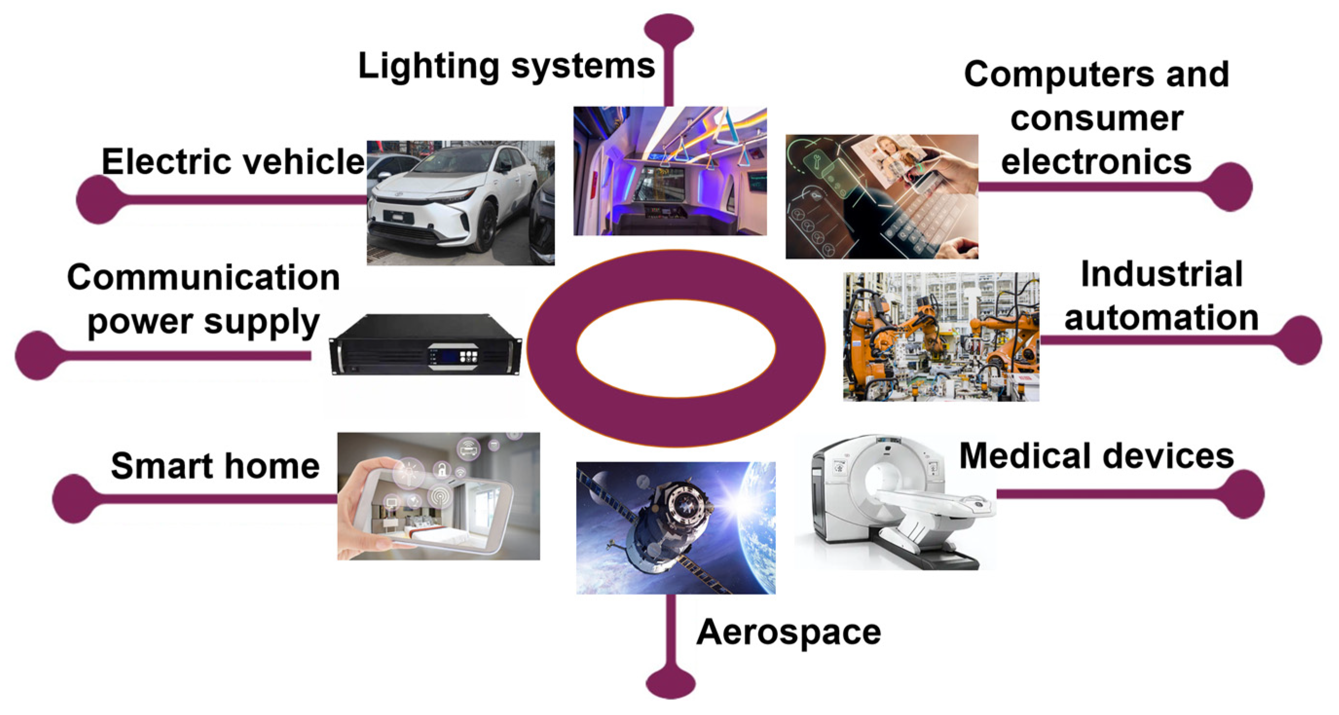
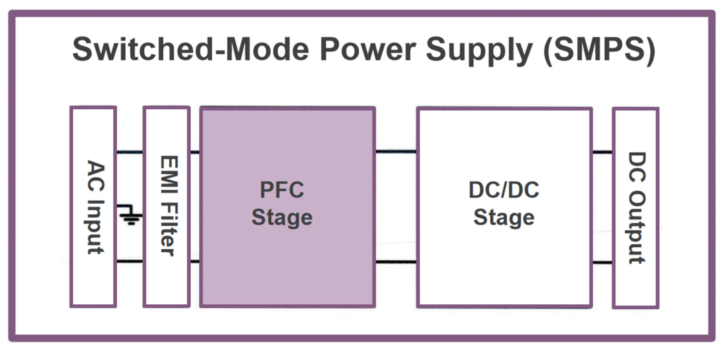
1. Introduction

| Topology | SD | M | FD | L | Co | Tot. Num |
|---|---|---|---|---|---|---|
| Conventional single switch | 4 | 1 | 1 | 1 | 1 | 8 |
| Dual boost bridgeless | 2 | 2 | 2 | 2 | 1 | 9 |
| Bi-directional bridgeless | 2 | 2 | 2 | 1 | 1 | 8 |
| totem-pole bridgeless | 2 | 2 | 0 | 1 | 1 | 6 |
| Comparative Elements | CCM | CRM | DCM |
|---|---|---|---|
| Inductor current | Continuous | Critical conduction | Discontinuous |
| Control methodology | Fixed frequency | Variable frequency | Fixed frequency/Variable frequency |
| Current ripple | Small | Relatively large | Large |
| Peak current | Small | Medium | Large |
| RMS current | Small | Medium | Large |
| Switching state | Hard switching | Soft switching | Soft switching |
- The inductance current ripple is larger in CRM, and the TCM control makes the inductance current ripple further increase;
- Power devices bear higher current stress, and inductors need to adopt larger core sizes to avoid saturation and power density reduction.
2. Research on Improvement Technology of Circuit Control Strategy
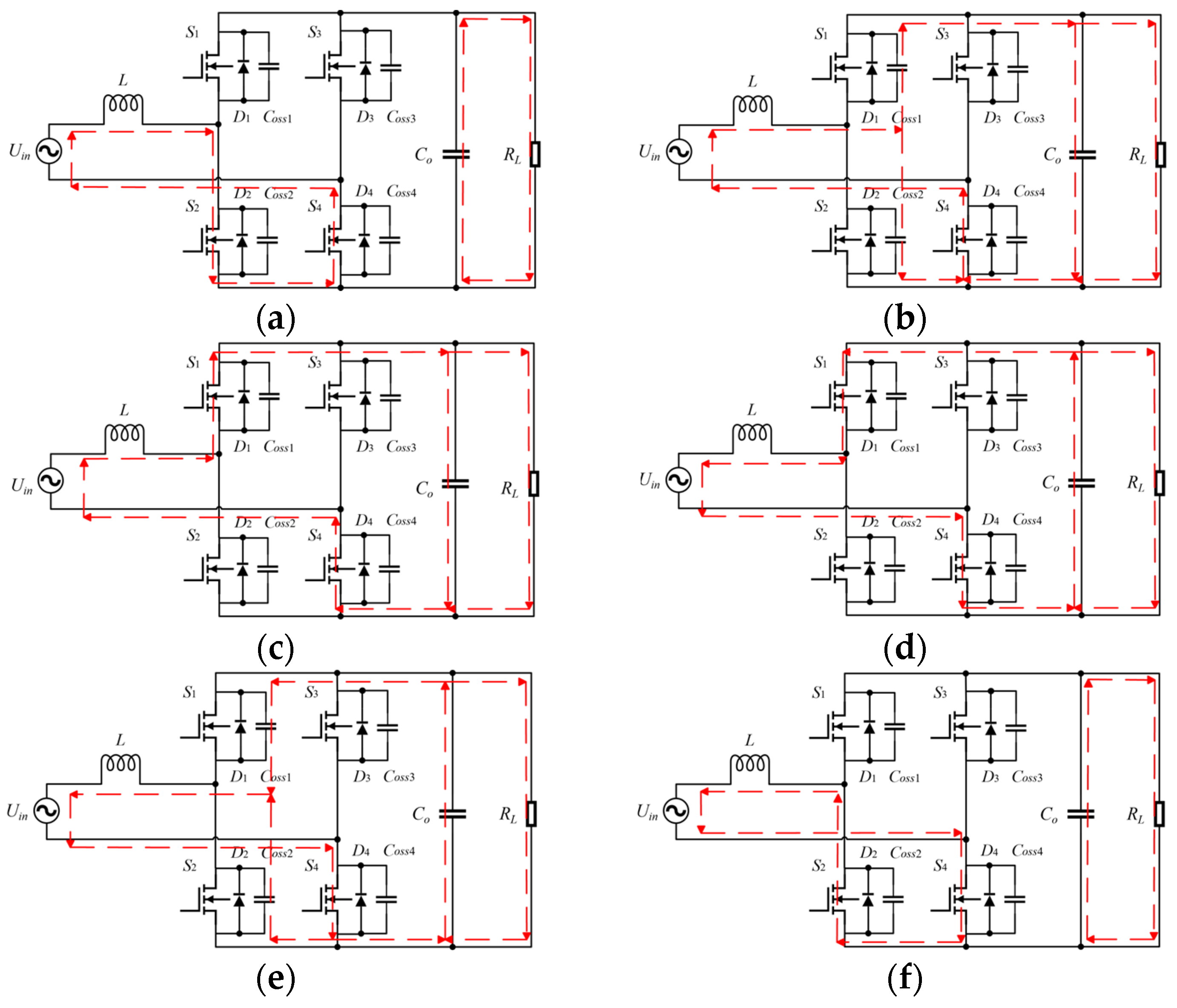
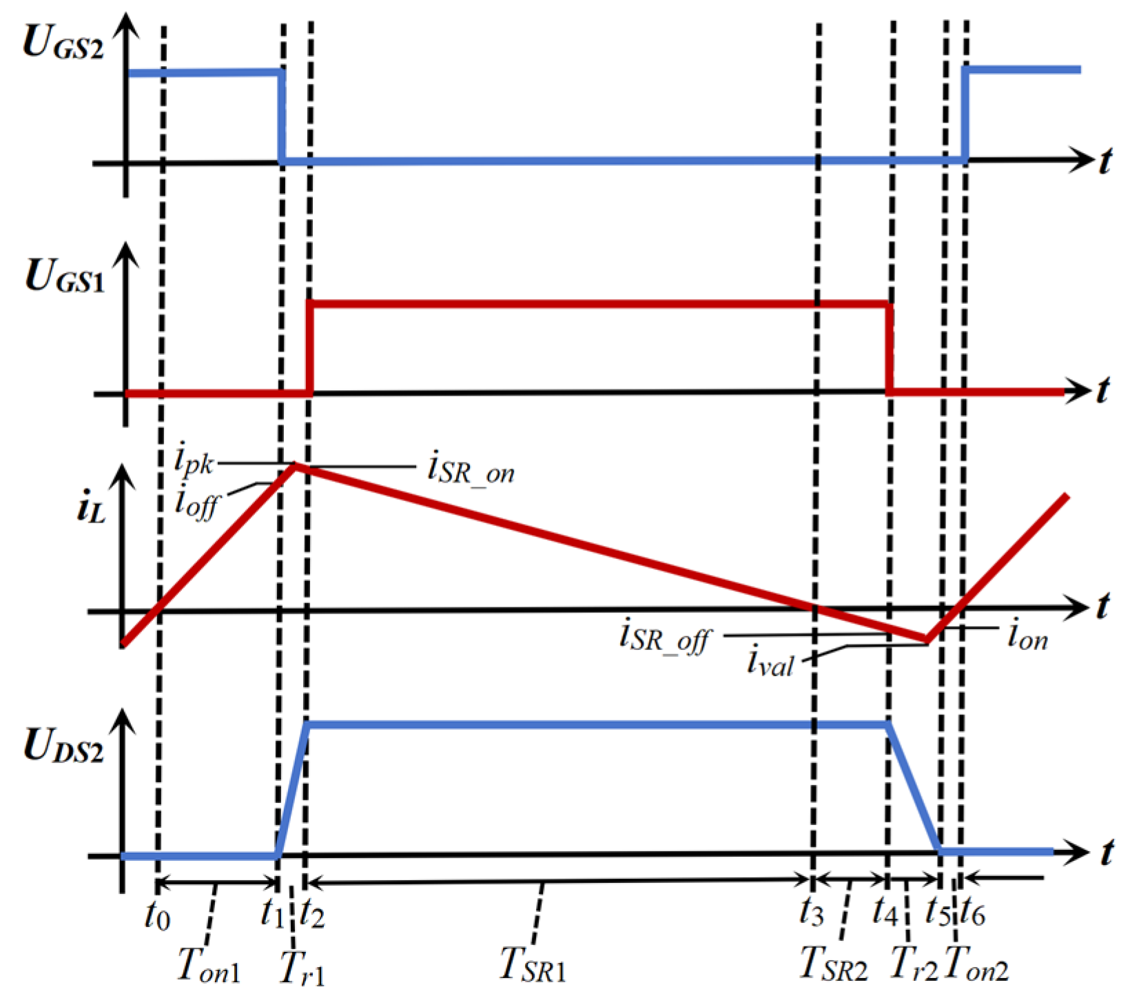
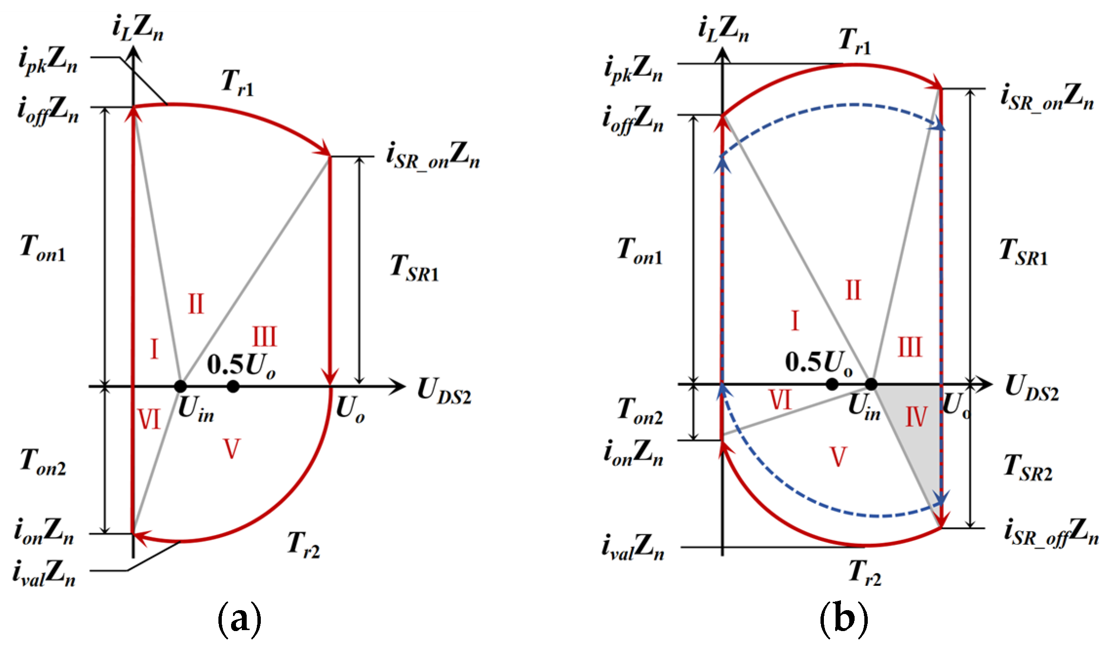
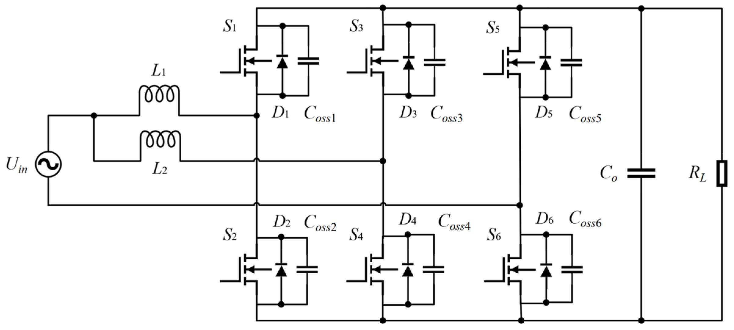
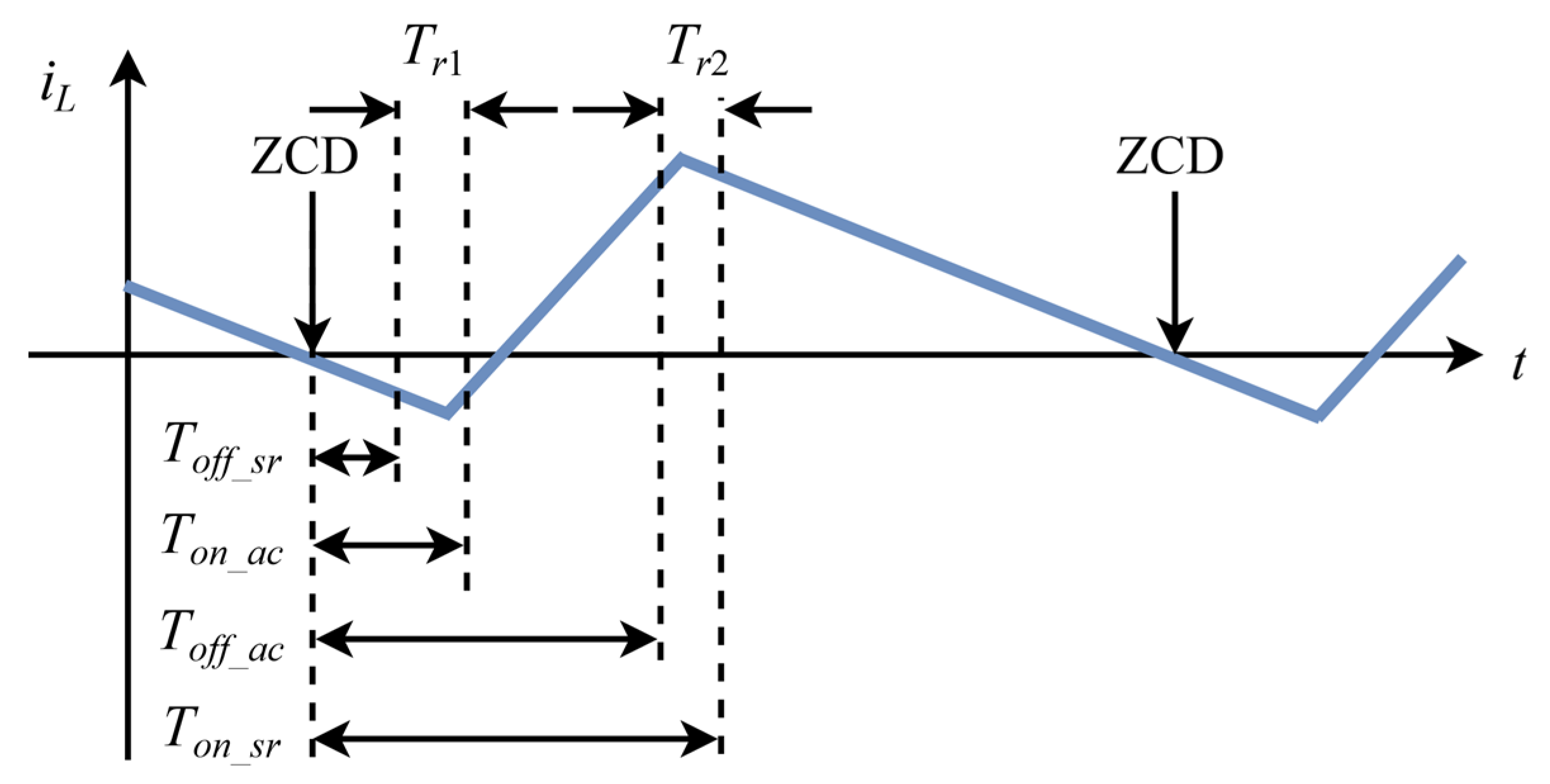
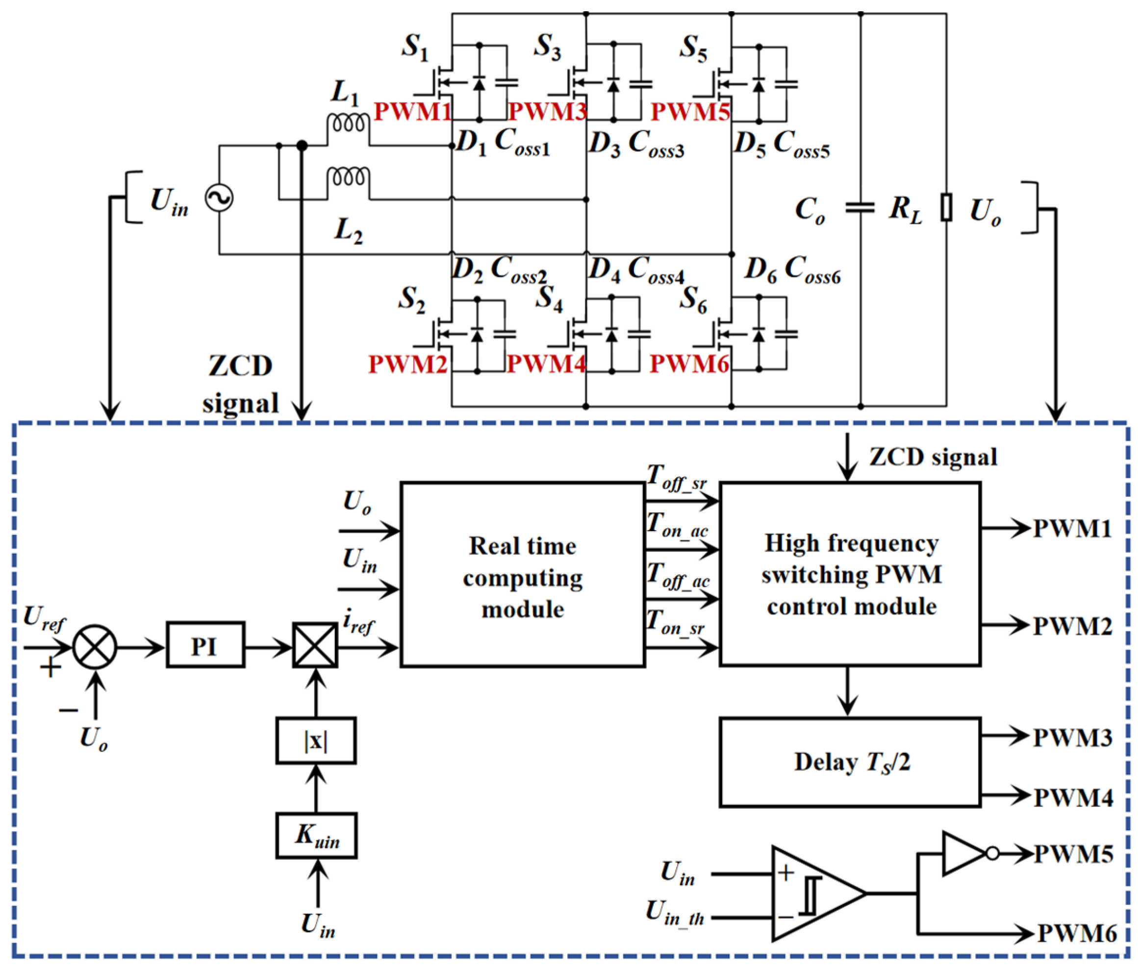
2.1. Working Principle of Circuit Based on TCM
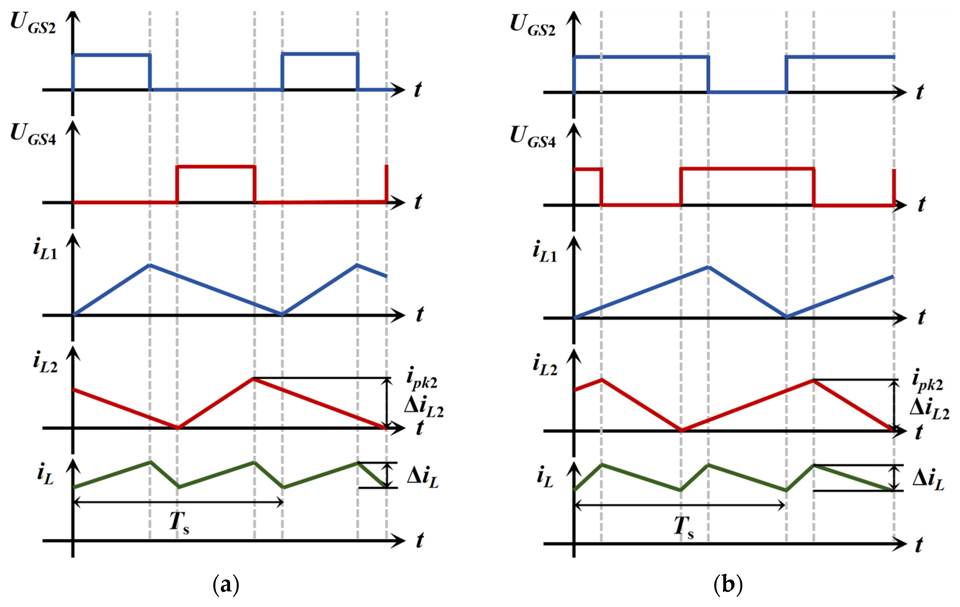
2.2. Two-Phase Interleaved Parallel Control
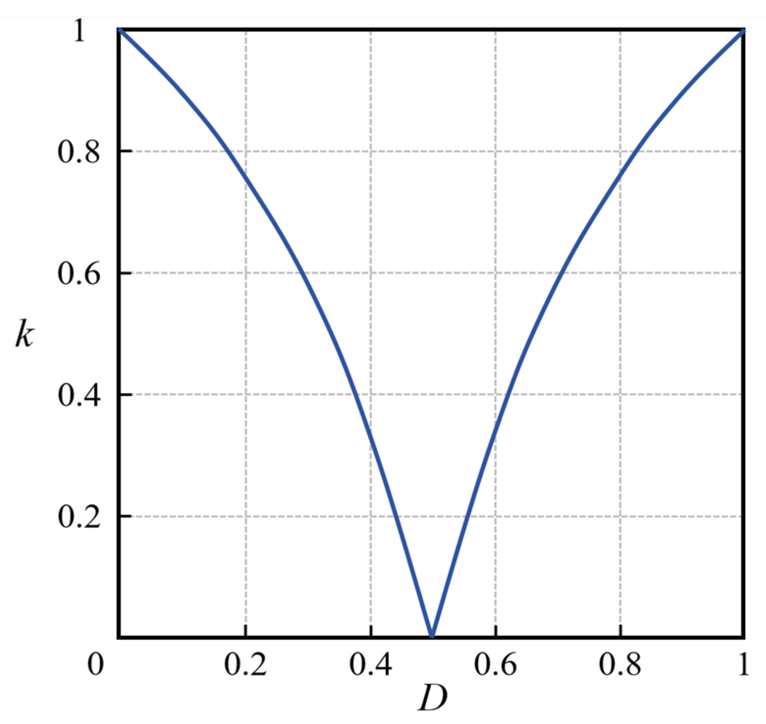
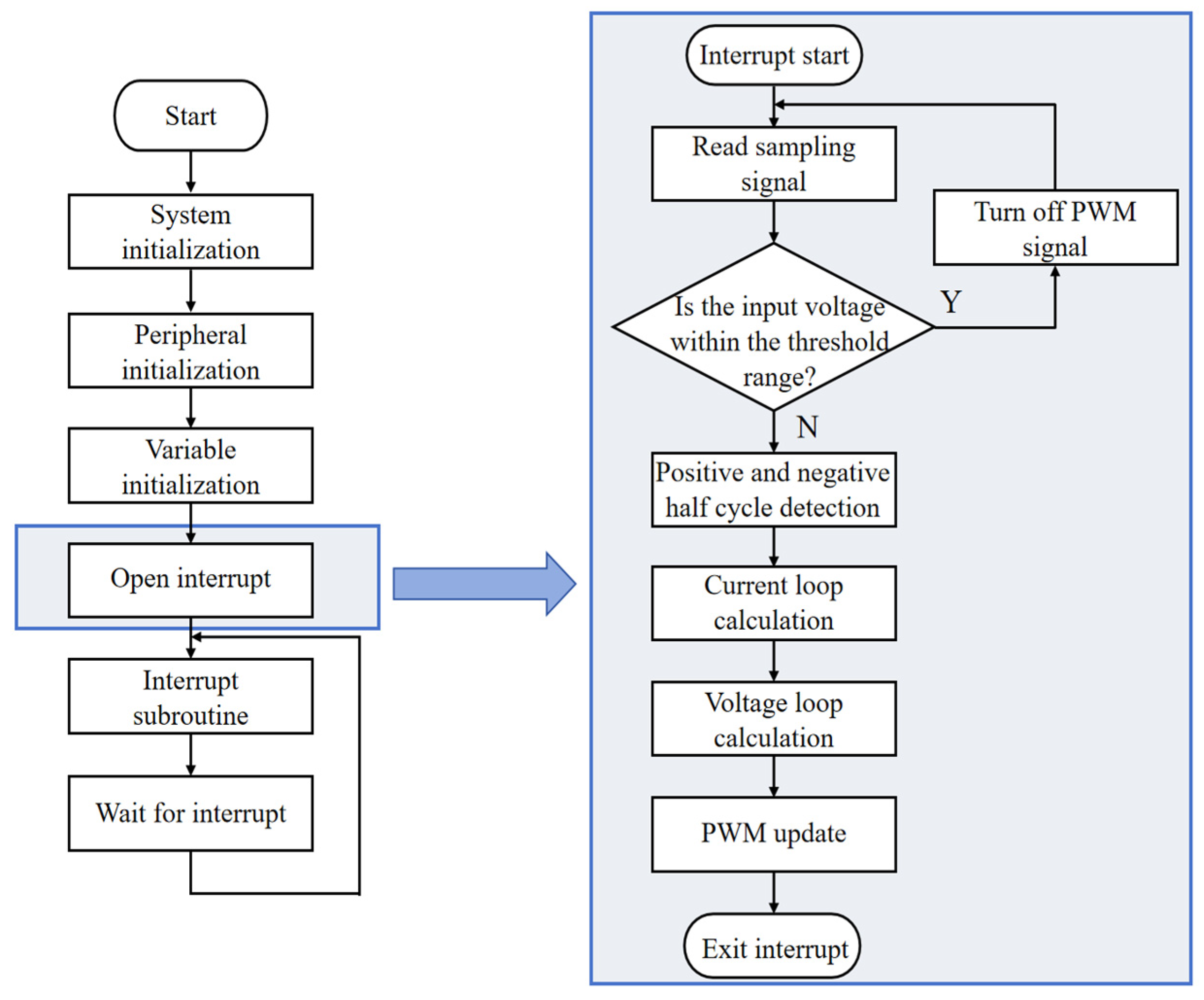
2.3. Control Implementation Strategy
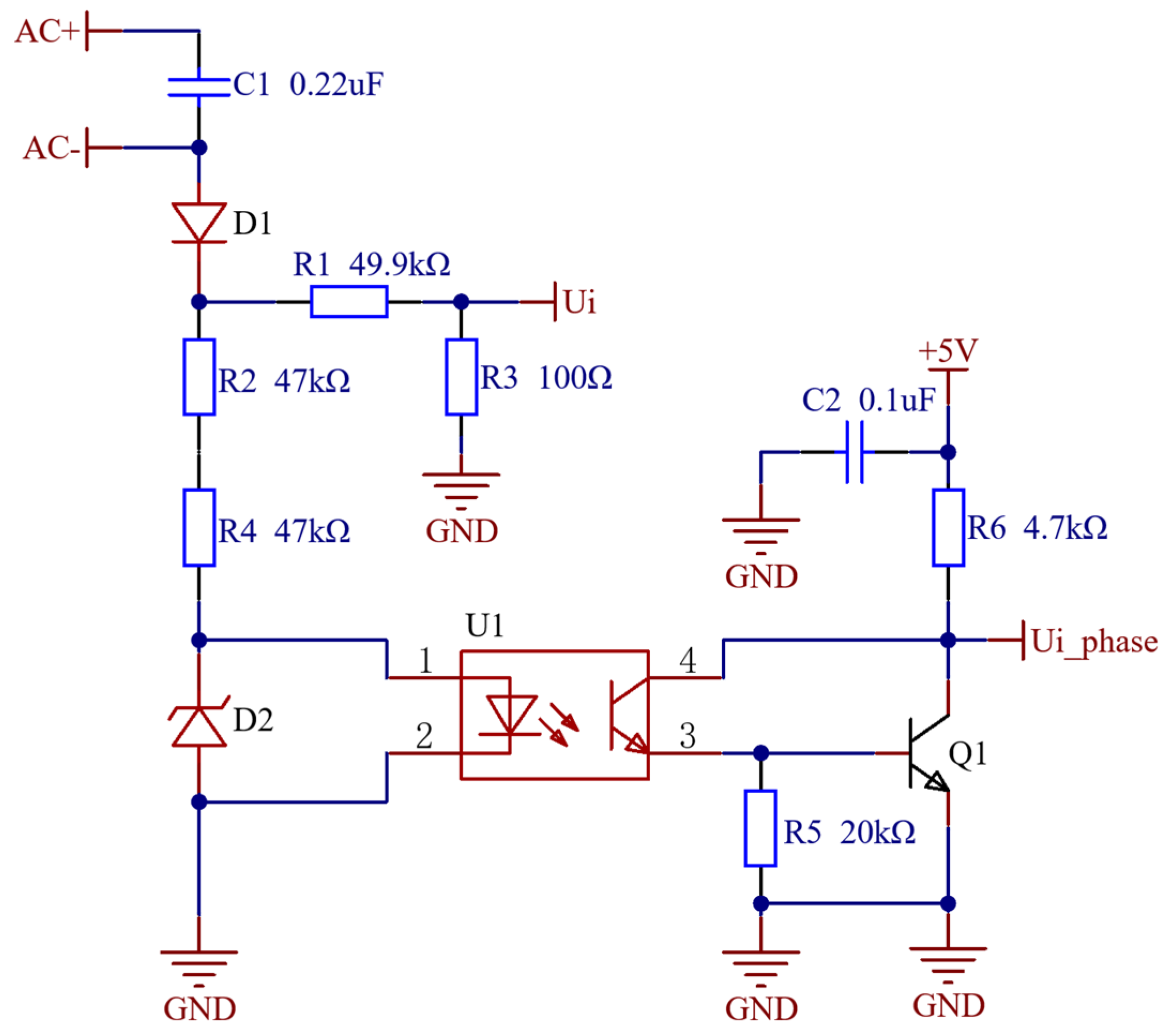
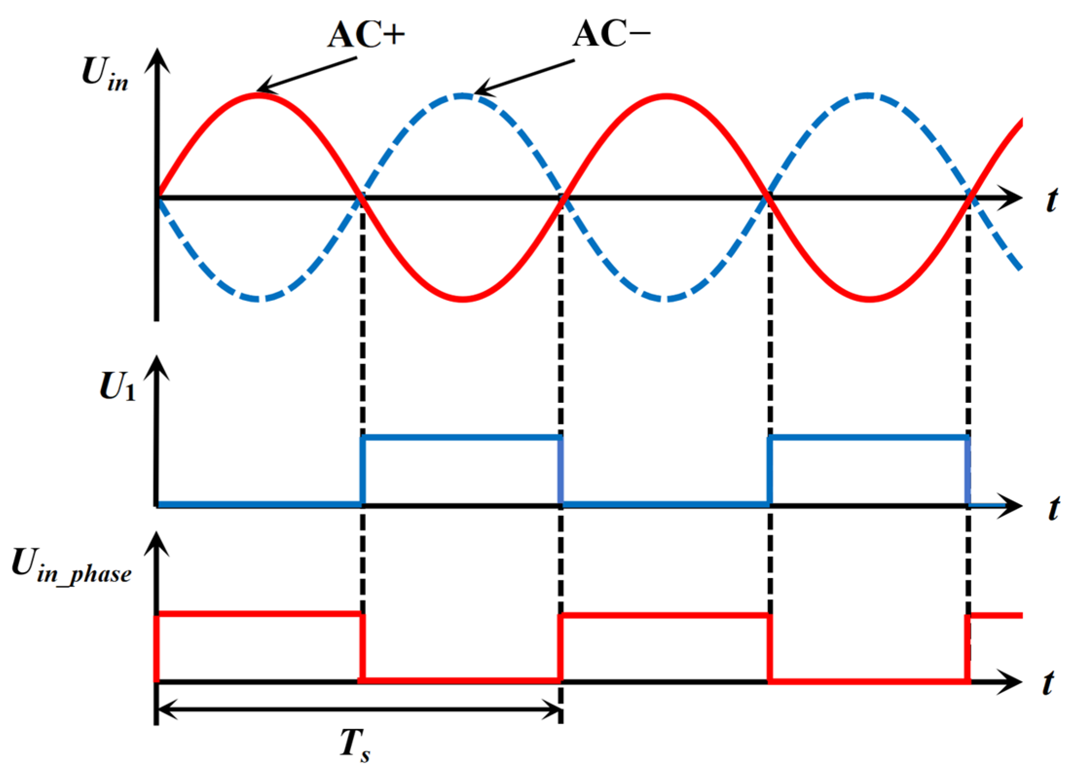
3. Optimal Design of AC Input Voltage Sampling Circuit
- There is no electrical connection between the input and output of the optocoupler through optical signal transmission. The isolation voltage of the optocoupler is generally 1~5 kV to achieve electrical isolation, which can isolate the common ground interference between the high-voltage side of input sampling and the low-voltage side of signal processing, as well as a series of signal interference such as grid fluctuation, motor interference, and other common mode noise that may exist;
- The optimized circuit enhances the synchronization of the voltage value and phase signal, reduces the number of components, and reduces the material cost;
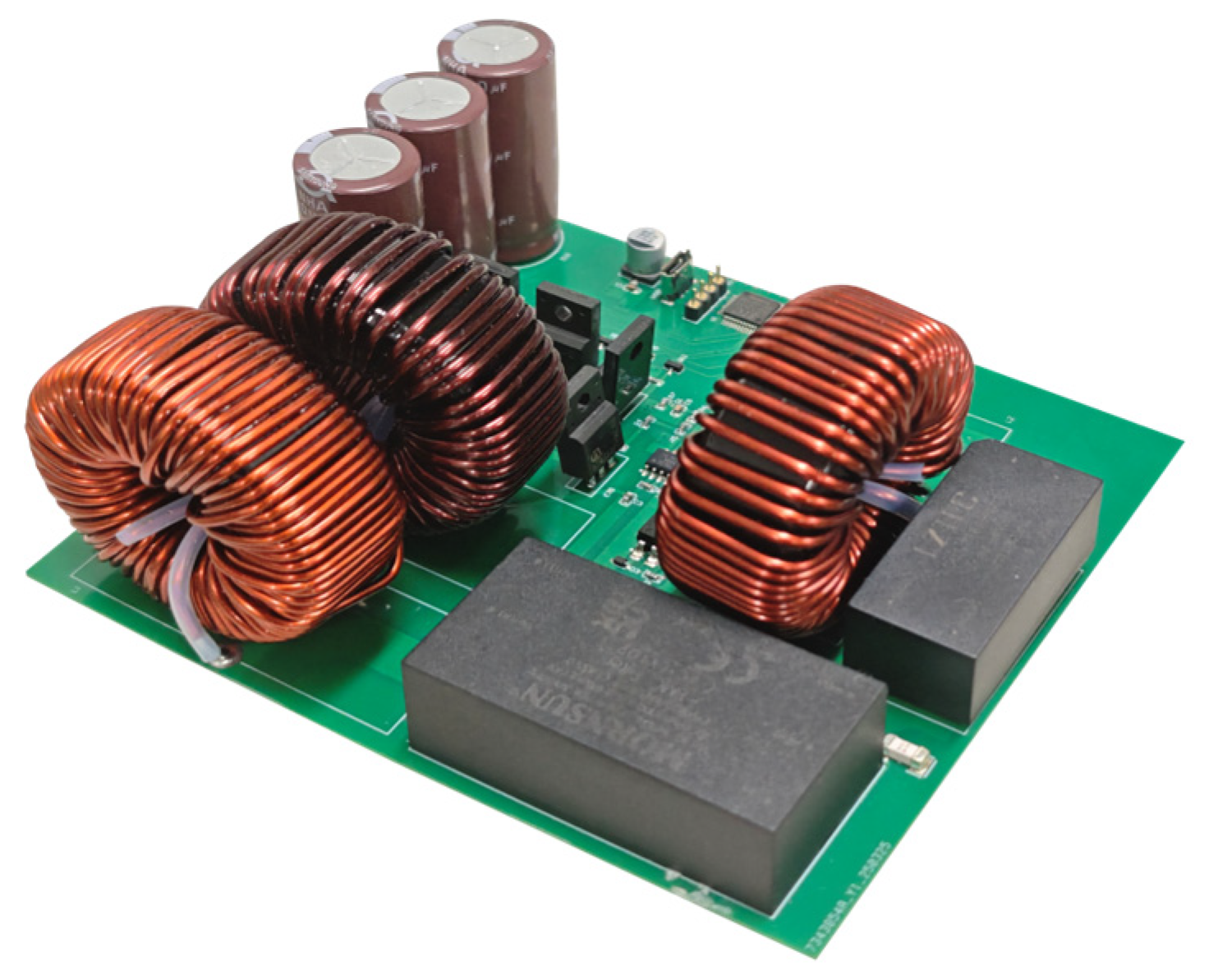
4. Experiment and Discussion
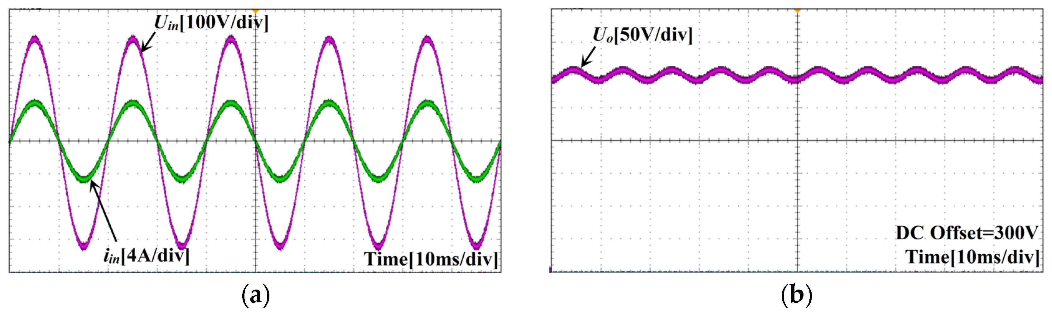
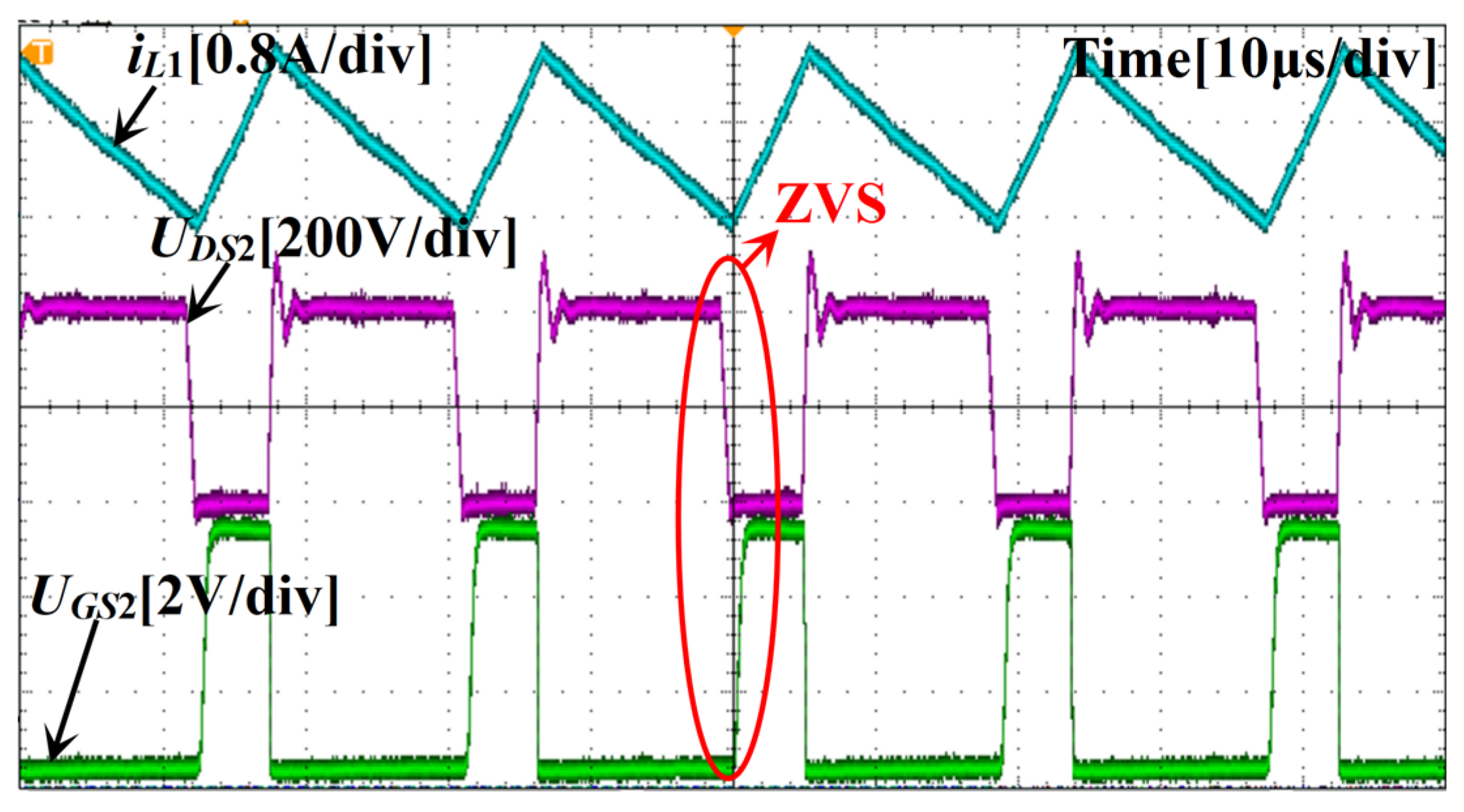
4.1. Simulation Analysis
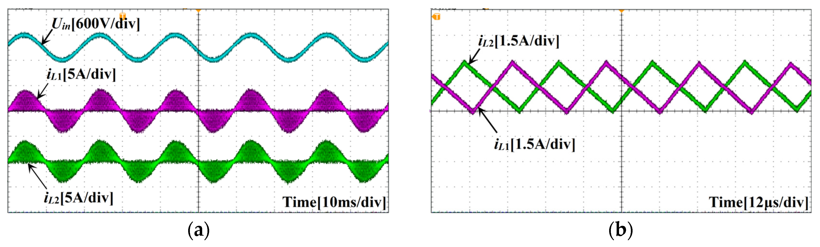
4.2. Empirical Test
5. Conclusions
Author Contributions
Funding
Data Availability Statement
Conflicts of Interest
Abbreviations
| PFC | Power Factor Correction |
| SMPS | Switching Mode Power Supply |
| TCM | Triangular Current Mode |
| CRM | Critical Conduction Mode |
| CCM | Continuous Current Mode |
| DCM | Discontinuous Current Mode |
| WBG | Wide-Bandgap |
| OBC | On-Board Charger |
| ZVS | Zero-Voltage Switching |
| VS | Valley Switching |
| ZCS | Zero-Current Switching |
| MCU | Microcontroller Unit |
| ZCD | Zero Crossing Detector |
| ADC | Analog-to-Digital Converter |
References
- Asa, E.; Xue, L.; Mohammad, M. A 1MHz Oak Ridge AC/DC Converter for UAV Contactless Charger Implementation. In Proceedings of the 2022 IEEE Applied Power Electronics Conference and Exposition (APEC), Houston, TX, USA, 20–24 March 2022. [Google Scholar] [CrossRef]
- Son, W.-J.; Lee, B.K. Design and Analysis of High Power Density On-Board Charger with Active Power Decoupling Circuit for Electric Vehicles. Energies 2023, 16, 7450. [Google Scholar] [CrossRef]
- Shahzad, D.; Farooq, M.; Pervaiz, S. A High-Power-Density High-Efficiency Soft-Switched Single-Phase Universal Input to 28-V Isolated AC-DC Converter Module Designed for Paralleled Operation. IEEE Trans. Power Electron. 2022, 37, 8262–8280. [Google Scholar] [CrossRef]
- Zhou, K.; Chen, S.-M.; Jin, N.-Z.; Sun, D.-Y. Research on Single-Phase and Three-Phase Compatible Isolated On-Board Charger and Control Technology. Energies 2022, 15, 6445. [Google Scholar] [CrossRef]
- Singh, B.; Singh, B.N.; Chandra, A.; Al-Haddad, K.; Pandey, A.; Kothari, D.P. A review of single-phase improved power quality AC-DC converters. IEEE Trans. Ind. Electron. 2003, 50, 962–981. [Google Scholar] [CrossRef]
- García, O.; Cobos, J.A.; Prieto, R. Single phase power factor correction: A survey. IEEE Trans. Power Electron. 2003, 18, 749–755. [Google Scholar] [CrossRef]
- IEC 61000-3-2. Consolidated Version. Available online: https://webstore.iec.ch/en/publication/18726 (accessed on 14 June 2025).
- GB/T 14549-1993. Quality of Electric Energy Supply-Harmonics Inpublic Supply. Available online: https://openstd.samr.gov.cn/bzgk/gb/newGbInfo?hcno=10A576E61901DA59E9A6AC555C2BAFD1 (accessed on 14 June 2025).
- IEEE 519-2014. IEEE Recommended Practice and Requirements for Harmonic Control in Electric Power Systems. Available online: https://standards.ieee.org/ieee/519/3710/ (accessed on 14 June 2025).
- Chen, F.-Z.; Maksimović, D. Digital control for improved efficiency and reduced harmonic distortion over wide load range in boost PFC rectifiers. IEEE Trans. Power Electron. 2010, 25, 2683–2692. [Google Scholar] [CrossRef]
- Lee, Y.-D.; Kim, C.-E.; Baek, J.-I.; Kim, D.-K.; Moon, G.-W. A Zero-Voltage-Switching Totem-pole Bridgeless Boost Power Factor Correction Rectifier having Minimized Conduction Losses. In Proceedings of the 2018 International Power Electronics Conference (IPEC-Niigata 2018-ECCE Asia), Niigata, Japan, 20–24 May 2018. [Google Scholar] [CrossRef]
- Li, B.; Zhang, R.; Zhao, N. GaN HEMT Driving Scheme of Totem-Pole Bridgeless PFC Converter. In Proceedings of the IEEE International Power Electronics and Application Conference and Exposition (IEEE PEAC), Shenzhen, China, 4–7 November 2018. [Google Scholar] [CrossRef]
- Zhang, R.; Liu, S.; Li, B. Totem-pole Bridgeless Boost PFC Converter Based on GaN HEMT for Air Conditioning Applications. In Proceedings of the 2nd IEEE Conference on Energy Internet and Energy System Integration (EI2), Beijing, China, 20–22 October 2018. [Google Scholar] [CrossRef]
- Shi, K.; Shoyama, M.; Tomioka, S. Common mode noise reduction in totem-pole bridgeless PFC converter. In Proceedings of the 2014 International Power Electronics and Application Conference and Exposition, Shanghai, China, 5–8 November 2014. [Google Scholar] [CrossRef]
- Han, J.-K. Efficiency and PF Improving Techniques with a Digital Control for Totem-Pole Bridgeless CRM Boost PFC Converters. Energies 2024, 17, 369. [Google Scholar] [CrossRef]
- Marxgut, C.; Biela, J.; Kolar, J.W. Interleaved triangular current mode (TCM) resonant transition, single phase PFC rectifier with high efficiency and high power density. In Proceedings of the IEEE International Power Electronics Conference (ECCE-Asia), Sapporo, Japan, 21–24 June 2010. [Google Scholar] [CrossRef]
- Biela, J.; Hassler, D.; Miniböck, J. Optimal design of a 5kW/dm3/98.3% efficient TCM resonant transition single-phase PFC rectifier. In Proceedings of the IEEE International Power Electronics Conference (ECCE-Asia), Sapporo, Japan, 21–24 June 2010. [Google Scholar] [CrossRef]
- Su, B.; Zhang, J.; Lu, Z. Totem-Pole Boost Bridgeless PFC Rectifier with Simple Zero- Current Detection and Full-Range ZVS Operating at the Boundary of DCM/CCM. IEEE Trans. Power Electron. 2011, 26, 427–435. [Google Scholar] [CrossRef]
- Zhu, K.; O’Grady, M.; Dodge, J. 1.5 kW single phase CCM totem-pole PFC using 650V SiC cascodes. In Proceedings of the 2016 IEEE 4th Workshop on Wide Bandgap Power Devices and Applications (WiPDA), Fayetteville, AR, USA, 7–9 November 2016. [Google Scholar] [CrossRef]
- Liu, Z.; Li, B.; Lee, F.C. Design of CRM AC/DC converter for very high-frequency high-density WBG-based 6.6 kW bidirectional on-board battery charger. In Proceedings of the 2016 IEEE Energy Conversion Congress and Exposition (ECCE), Milwaukee, WI, USA, 18–22 September 2016. [Google Scholar] [CrossRef]
- Li, H.; Zhang, Z.; Wang, S. A 300-kHz 6.6-kW SiC Bidirectional LLC Onboard Charger. IEEE Trans. Ind. Electron. 2020, 67, 1435–1445. [Google Scholar] [CrossRef]
- Liu, Z.; Huang, X.; Mu, M. Design and evaluation of GaN-based dual-phase interleaved MHz critical mode PFC converter. In Proceedings of the 2014 IEEE Energy Conversion Congress and Exposition (ECCE), Pittsburgh, PA, USA, 14–18 September 2014. [Google Scholar] [CrossRef]
- Le, H.N.; Itoh, J.-I. Wide-Load-Range Efficiency Improvement for High-Frequency SiC-Based Boost Converter with Hybrid Discontinuous Current Mode. IEEE Trans. Power Electron. 2018, 33, 1843–1854. [Google Scholar] [CrossRef]
- Huang, Q.; Yu, R.; Ma, Q. Predictive ZVS Control with Improved ZVS Time Margin and Limited Variable Frequency Range for a 99% Efficient, 130-W/in3 MHz GaN Totem-Pole PFC Rectifier. IEEE Trans. Power Electron. 2019, 34, 7079–7091. [Google Scholar] [CrossRef]
- Tang, Y.; Ding, W.; Khaligh, A. A bridgeless totem-pole interleaved PFC converter for plug-in electric vehicles. In Proceedings of the 2016 IEEE Applied Power Electronics Conference and Exposition (APEC), Long Beach, CA, USA, 20–24 March 2016. [Google Scholar] [CrossRef]
- Cho, J.-H.; Kim, D.-K.; Bae, H.-H. A Fully Integrated Multi-Phase Buck Converter with On-Chip Capacitor Dynamic Re-Allocation and Fine-Grained Phase-Shedding Techniques. IEEE J. Solid-State Circuits 2022, 57, 3840–3852. [Google Scholar] [CrossRef]
- Dudak, A.T.; Bakan, A.F. A Digital Iterative Learning Based Peak Current Mode Control for Interleaved totem-pole PFC Circuit. Energies 2024, 17, 5026. [Google Scholar] [CrossRef]
- Ye, Z.; Zhu, D.; Yang, H. Totem-Pole PFC Reliability and Performance Improvement with Advanced Controls. IEEE Power Electron. Mag. 2022, 9, 37–44. [Google Scholar] [CrossRef]
- Wen, Y.; Ruan, L. Stability analysis of voltage sampling circuits applied to switching mode power supply with fully-immersed evaporative cooling. In Proceedings of the 2017 20th International Conference on Electrical Machines and Systems (ICEMS), Sydney, NSW, Australia, 11–14 August 2017. [Google Scholar] [CrossRef]
- Yang, C.; Zheng, S.; Feng, R. Design and Implementation of the Anti-noise High Precision Voltage/Current Data Acquisition System. In Proceedings of the 2020 15th IEEE Conference on Industrial Electronics and Applications (ICIEA), Kristiansand, Norway, 9–13 November 2020. [Google Scholar] [CrossRef]
- Motahari, M.; Daneshvar, A.R.; Tahami, F. A Comparative Analysis of the Reliability of Auxiliary Power Supplies. In Proceedings of the 2025 16th Power Electronics, Drive Systems, and Technologies Conference (PEDSTC), Tabriz, Iran, 4–6 February 2025. [Google Scholar] [CrossRef]
- Kaunkid, S.; Aurasopon, A.; Khamsen, W.; Takeang, C.; Piladaeng, N.; Lloret, J. Resistive Measurement Method for MQ Sensors Based on ADCs of Microcontrollers. IEEE Access 2024, 12, 144364–144376. [Google Scholar] [CrossRef]
- Li, Y.; Chen, H. Design Optimization of Low-Power Microelectronic Circuits Based on CMOS Technology. In Proceedings of the 2025 5th International Conference on Consumer Electronics and Computer Engineering (ICCECE), Dongguan, China, 28 February–2 March 2025. [Google Scholar] [CrossRef]
- Ali, F.B.; Dahman, H.; El Mir, L. Design and Realization of a Temperature Measurement and Control System Adapted to Gas Nanosensors. In Proceedings of the 2025 IEEE 22nd International Multi-Conference on Systems, Signals & Devices (SSD), Monastir, Tunisia, 17–20 February 2025. [Google Scholar] [CrossRef]
- Mikulka, J.; Dušek, J.; Dědková, J.; Pařilková, J.; Műnsterová, Z. A Fast and Low-cost Measuring System for Electrical Impedance Tomography. In Proceedings of the 2019 PhotonIcs & Electromagnetics Research Symposium-Spring (PIERS-Spring), Rome, Italy, 17–20 June 2019. [Google Scholar] [CrossRef]
- Jing, B.; Liu, F.; Li, G.; Xiong, G. Development of a low-power switching signal acquisition device. In Proceedings of the 2023 10th International Forum on Electrical Engineering and Automation (IFEEA), Nanjing, China, 3–5 November 2023. [Google Scholar] [CrossRef]


| Parameter | Value |
|---|---|
| Forward voltage drop | 1.2 V |
| Rise time | 4 μs |
| Fall time | 3 μs |
| Output current | 50 mA |
| Isolation voltage | 5 kV |
| Parameter | Value |
|---|---|
| Output power Po | 600 W |
| Input voltage Uin_rms | 220 V |
| Output voltage Uo | 400 V |
| Maximum switching frequency fs_max | 100 kHz |
| Input voltage frequency fline | 50 Hz |
| Branch inductor L1 and L2 | 1 mH |
| Output capacitor Co | 500 μF |
| Article | Single-Phase/Interleaved | The iL Needs to Be Sampled | Controller | Rated Power | Peak Efficiency |
|---|---|---|---|---|---|
| [24] | Single-phase | Yes | DSP | 1.6 kW | 99% |
| [17] | Single-phase | No | DSP + CPLD | 3 kW | 98.3% |
| [18] | Single-phase | No | Unknown | 350 W | 98.4% |
| [16] | Interleaved | No | DSP + FPGA | 200 W | 96.9% |
| Proposed | Interleaved | No | MCU | 600 W | 97.3% |
Disclaimer/Publisher’s Note: The statements, opinions and data contained in all publications are solely those of the individual author(s) and contributor(s) and not of MDPI and/or the editor(s). MDPI and/or the editor(s) disclaim responsibility for any injury to people or property resulting from any ideas, methods, instructions or products referred to in the content. |
© 2025 by the authors. Licensee MDPI, Basel, Switzerland. This article is an open access article distributed under the terms and conditions of the Creative Commons Attribution (CC BY) license (https://creativecommons.org/licenses/by/4.0/).
Share and Cite
Niu, P.; Guo, J.; Gao, Z.; Yan, J.; Gao, S. Research on Improved Technology of Totem-Pole Bridgeless PFC Circuit Based on Triangular Current Mode. Energies 2025, 18, 3886. https://doi.org/10.3390/en18143886
Niu P, Guo J, Gao Z, Yan J, Gao S. Research on Improved Technology of Totem-Pole Bridgeless PFC Circuit Based on Triangular Current Mode. Energies. 2025; 18(14):3886. https://doi.org/10.3390/en18143886
Chicago/Turabian StyleNiu, Pingjuan, Jingying Guo, Zhigang Gao, Jingwen Yan, and Shengwei Gao. 2025. "Research on Improved Technology of Totem-Pole Bridgeless PFC Circuit Based on Triangular Current Mode" Energies 18, no. 14: 3886. https://doi.org/10.3390/en18143886
APA StyleNiu, P., Guo, J., Gao, Z., Yan, J., & Gao, S. (2025). Research on Improved Technology of Totem-Pole Bridgeless PFC Circuit Based on Triangular Current Mode. Energies, 18(14), 3886. https://doi.org/10.3390/en18143886