
Design and Development of a New Long-Pulse-Width Power Supply

Abstract
1. Introduction
1.1. Background
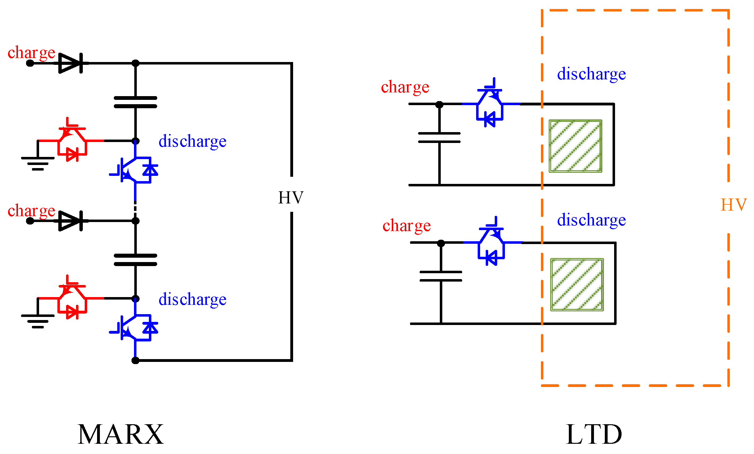
1.2. Related Works
1.3. Contributions and Addressed Gaps
1.4. Paper Outline
2. Methodology
2.1. Operating Characteristics of LCC Resonant Converter
2.2. Working Mode Analysis of LCC Converter
2.3. Control Scheme
2.4. Prototype Design and Simulation Analysis
2.5. Component Parameter Design and Selection
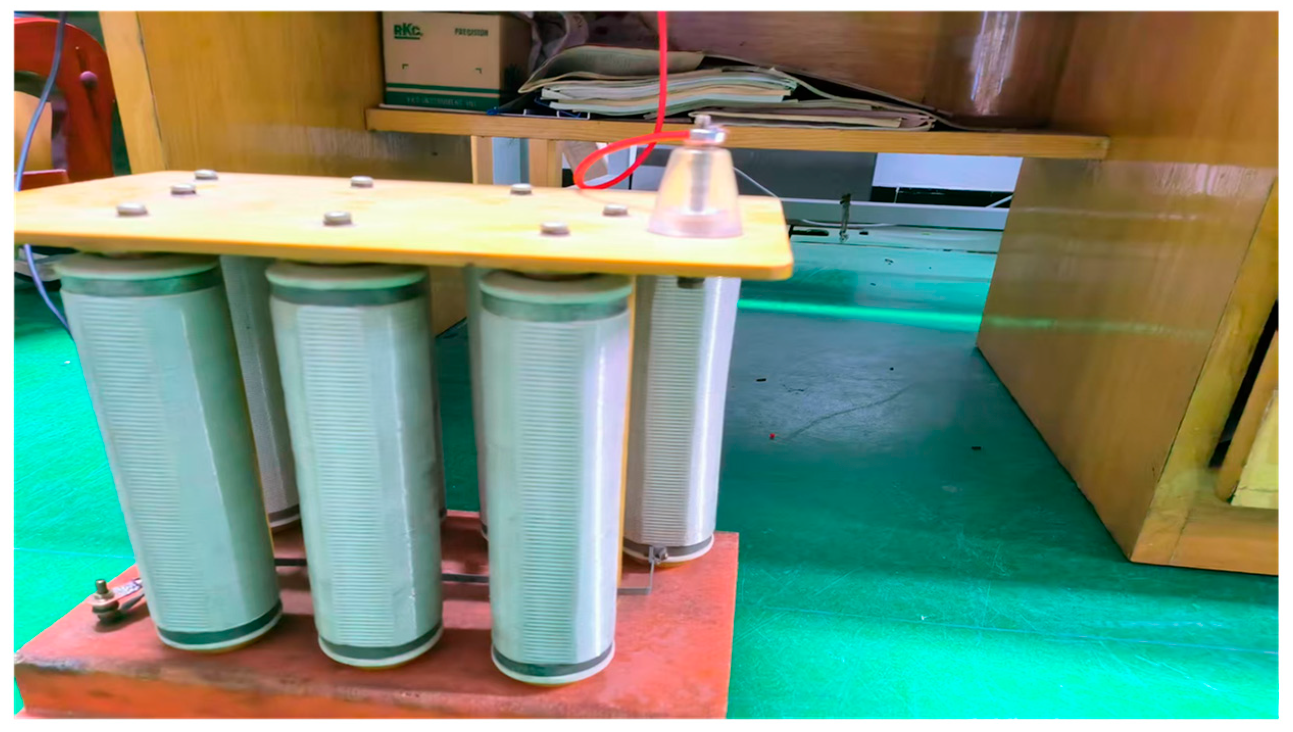
2.6. Design and Measurement of High-Frequency Transformer
2.7. EMI/EMC Performance Analysis and Series IGBT Design
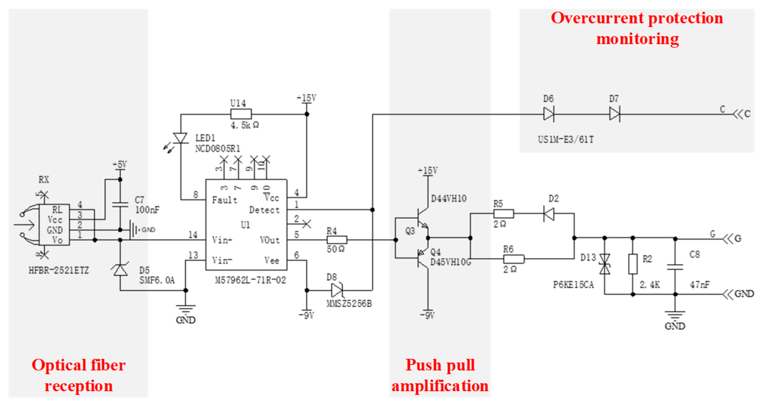
2.8. Optical Fiber Isolation Drive Design
3. Results
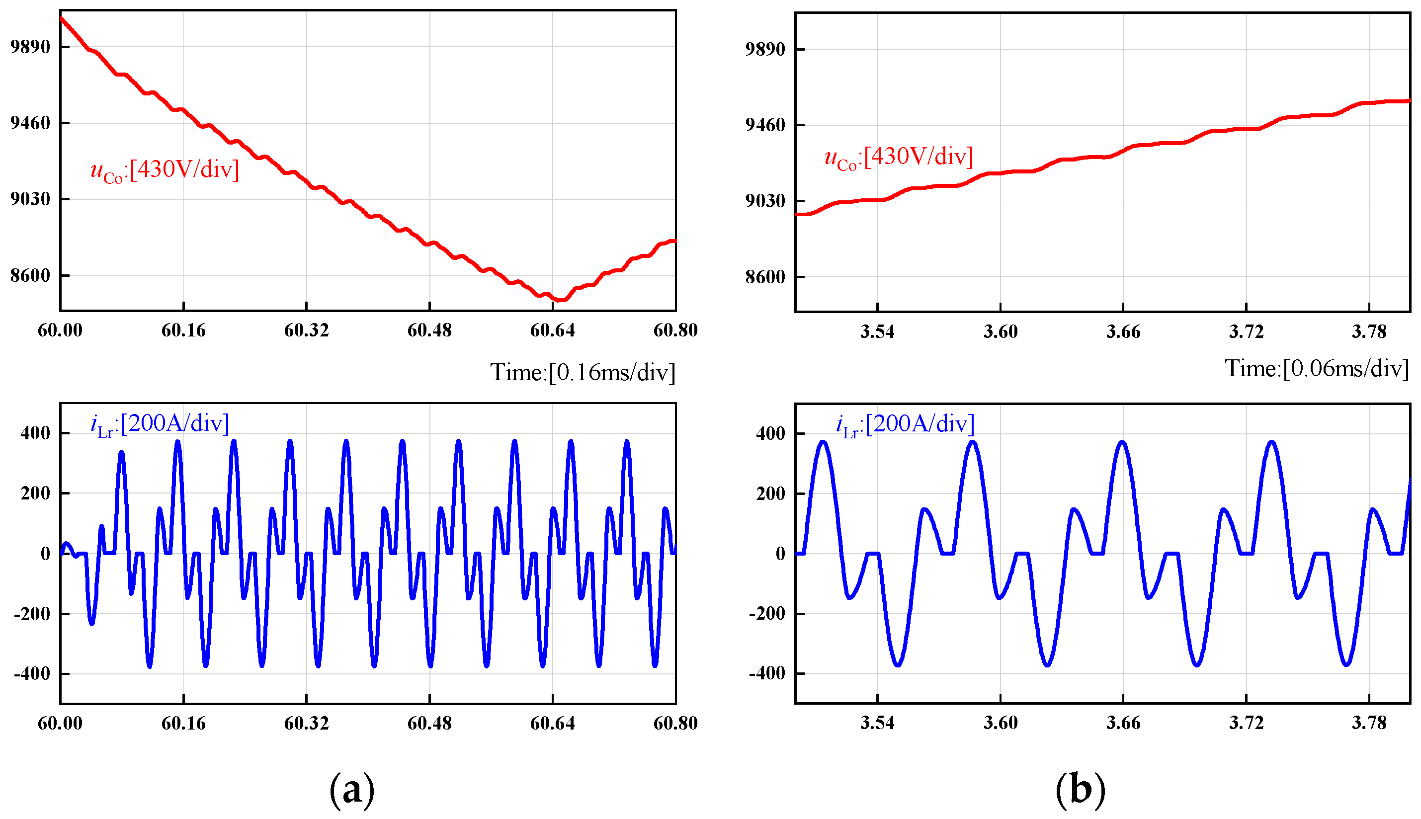
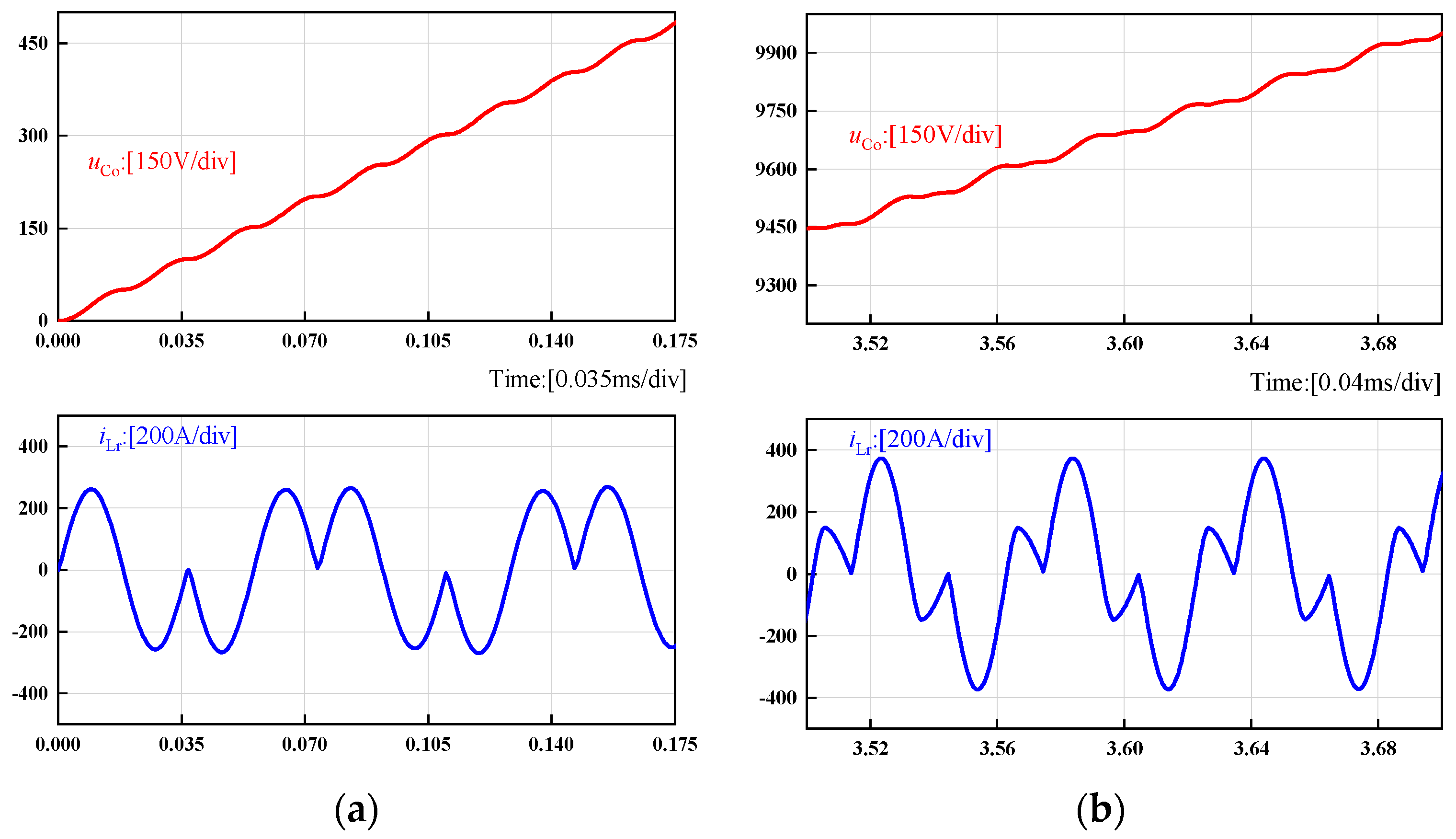
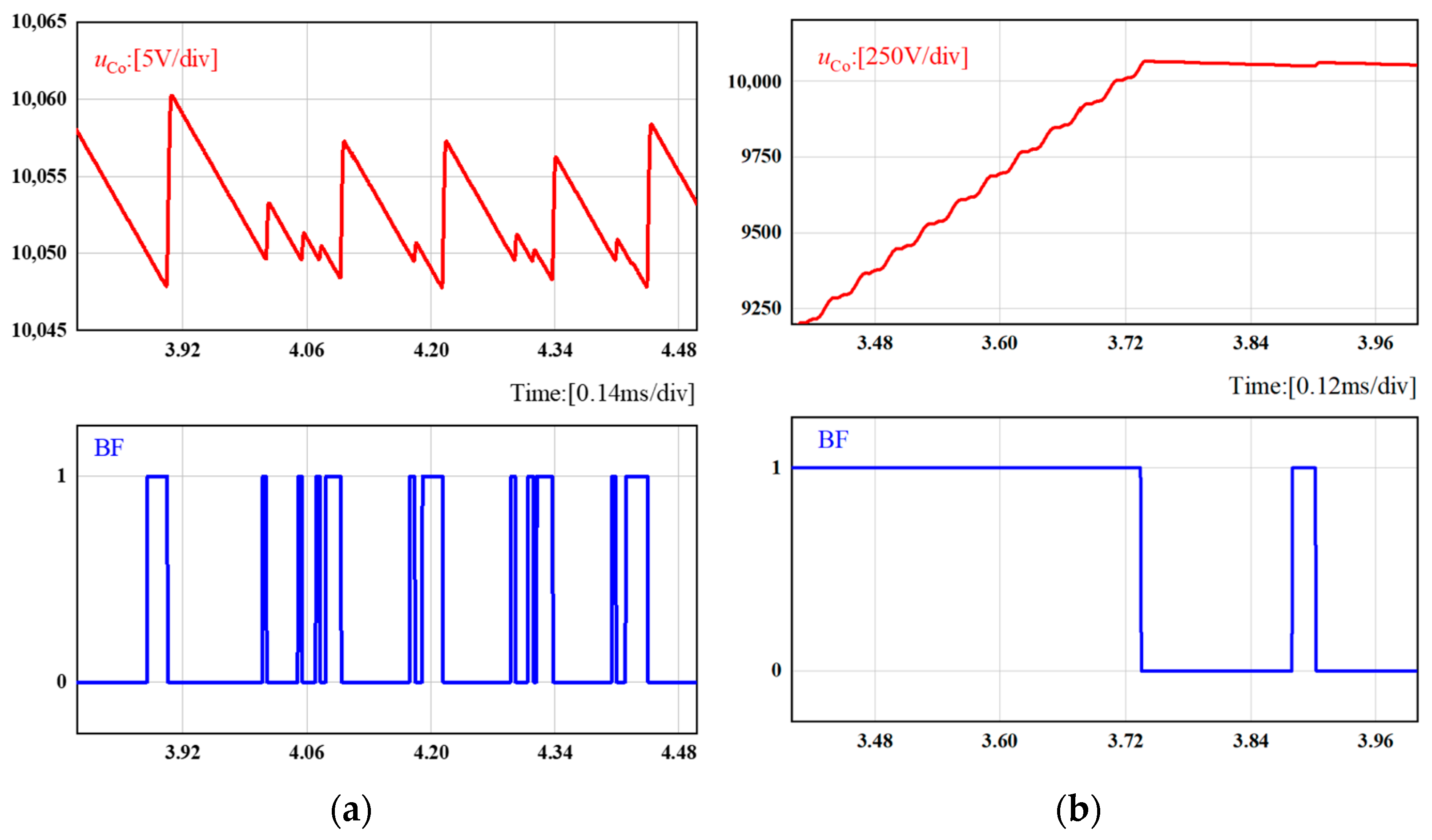
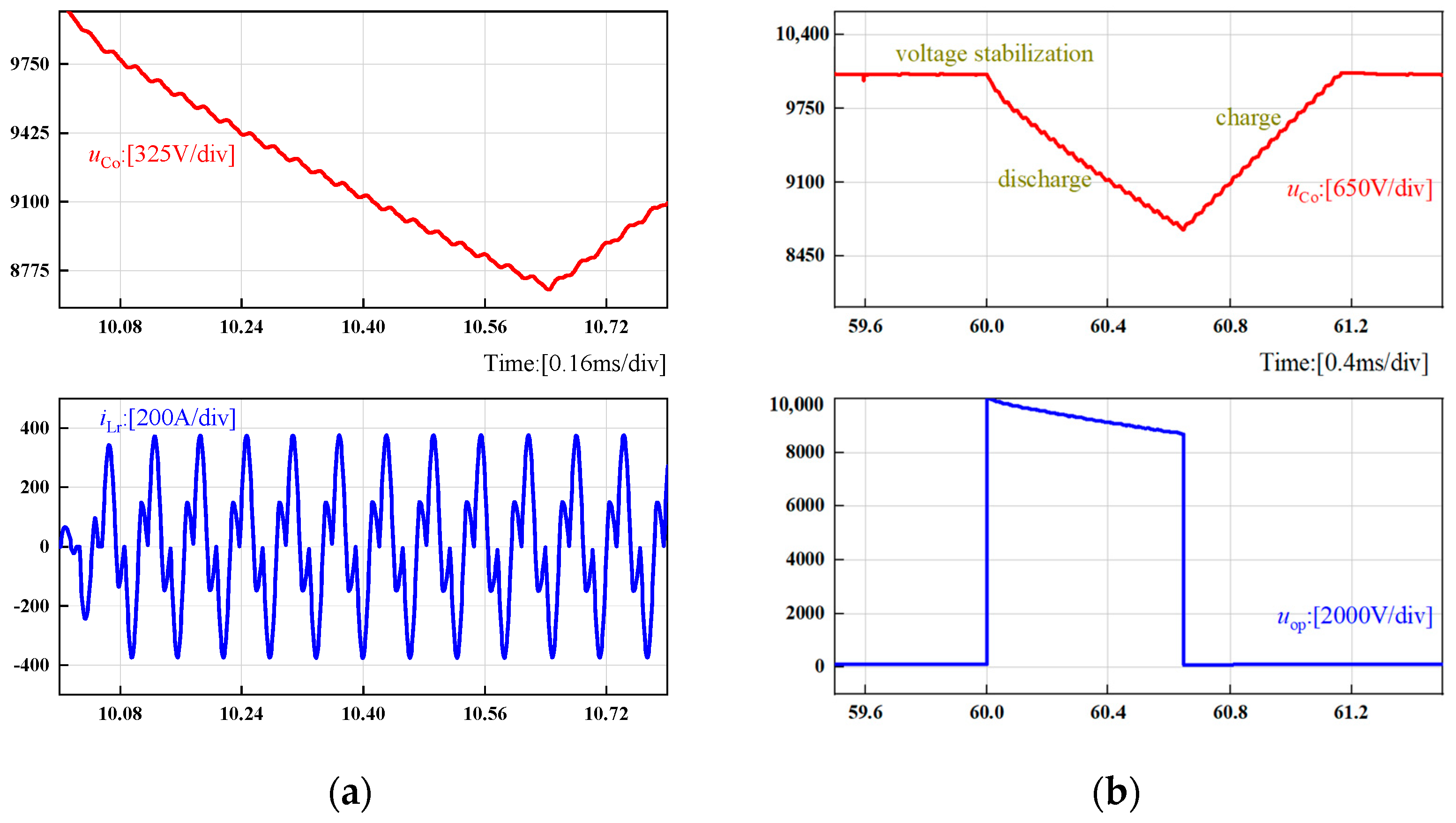
3.1. Simulation Analysis
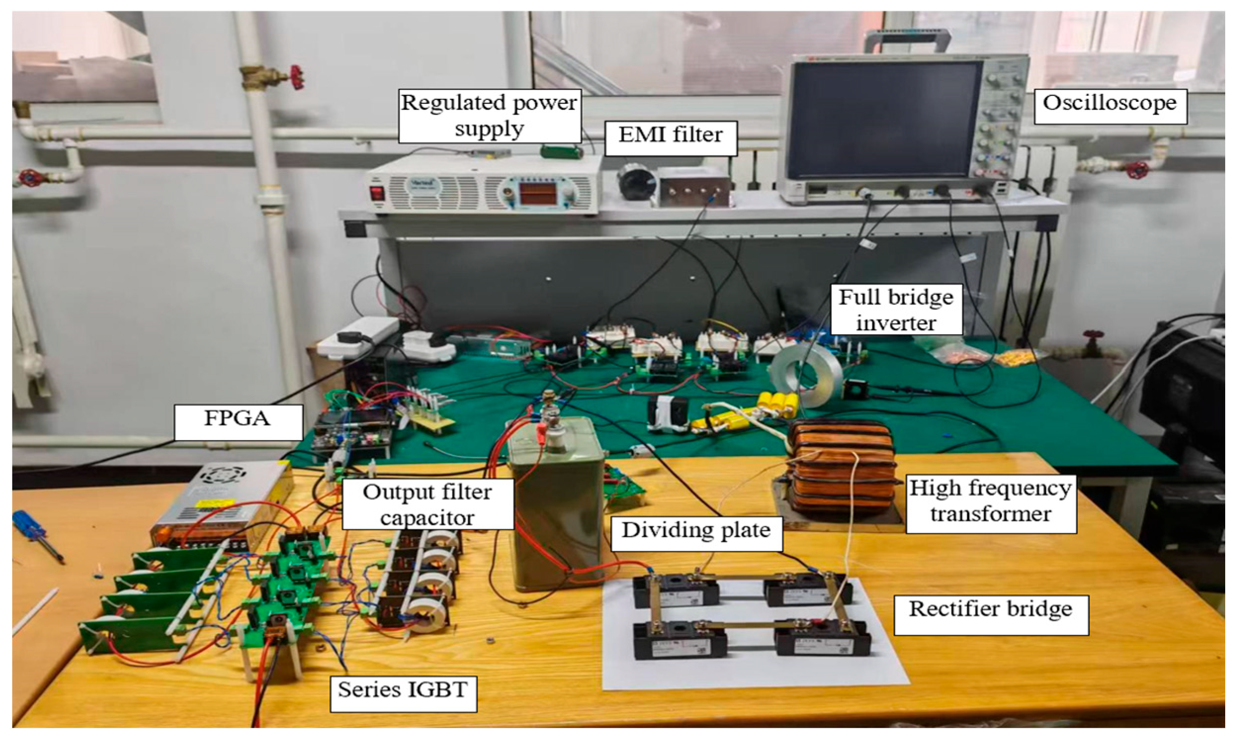
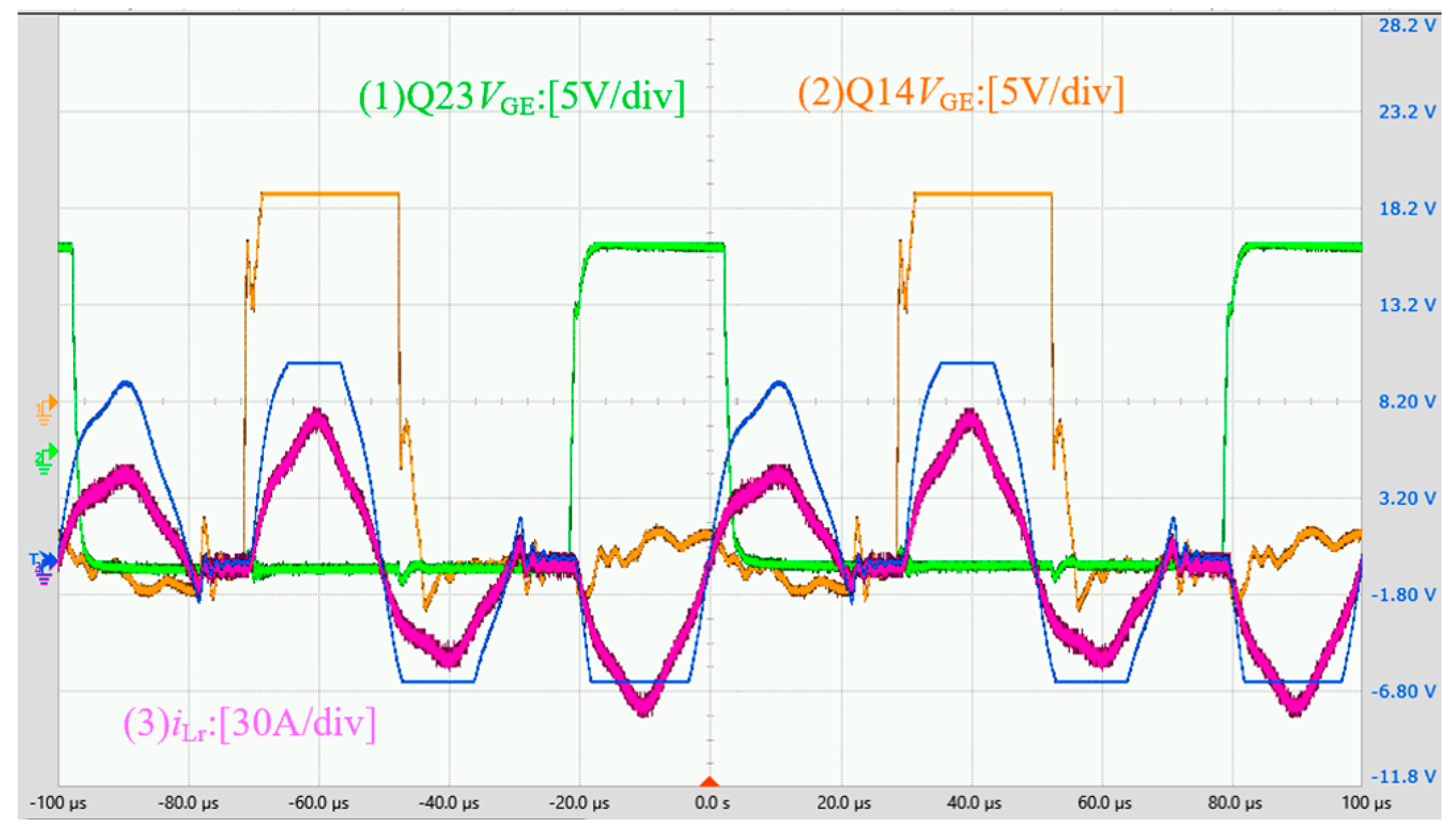
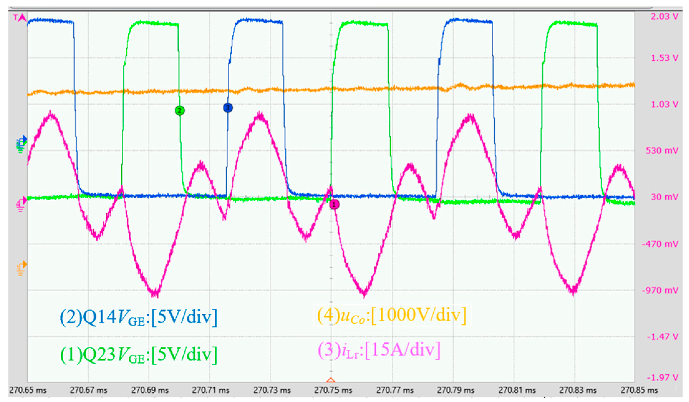
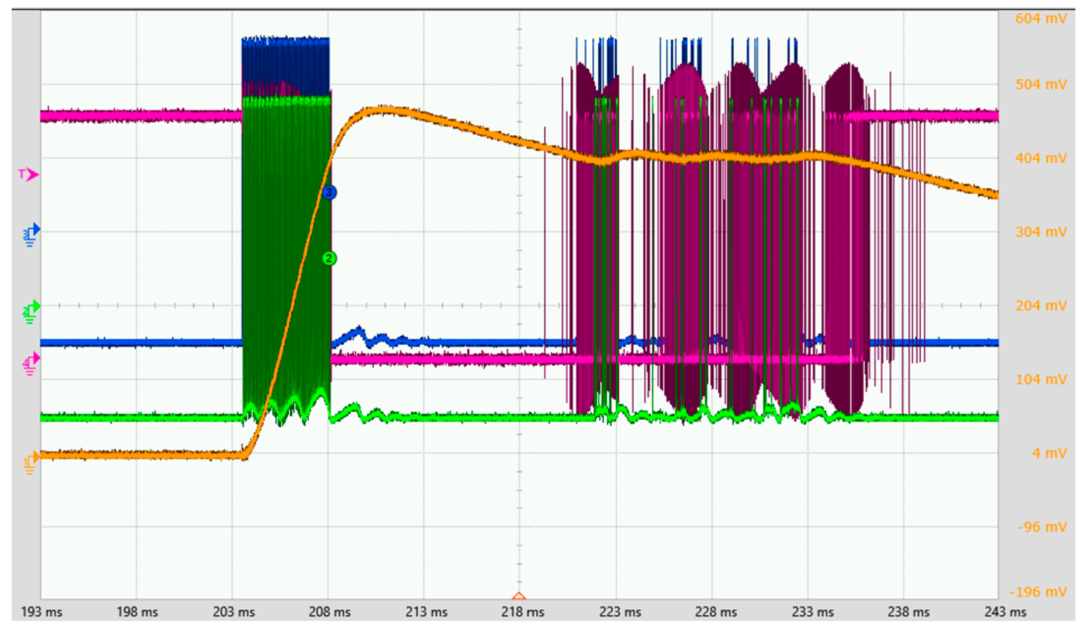
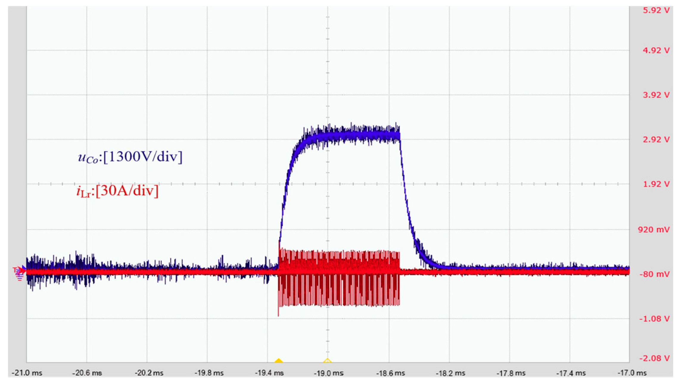
3.2. Experimental Test and Verification
3.3. Cost Assembly Complexity Analysis
4. Conclusions
Author Contributions
Funding
Data Availability Statement
Conflicts of Interest
References
- Michael, G.; Jon, M. Rapid Capacitor Charger with Advanced Digital Control. In Proceedings of the 2021 IEEE Pulsed Power Conference (PPC), Denver, CO, USA, 12–16 December 2021; pp. 1–3. [Google Scholar]
- Hai, R.; Gao, F.; Wei, S.; Li, R.; Lin, Z.; Philip, M. Thermal Buffering Effect of Phase Change Material on Press-pack IGBT during Power Pulse. In Proceedings of the 2019 IEEE Energy Conversion Congress and Exposition (ECCE), Baltimore, MD, USA, 29 September–3 October 2019; pp. 4937–4943. [Google Scholar]
- Ohkami, T.; Souda, M.; Saito, T.; Yamazaki, C.; Asano, S.; Suzuki, Y. Development of a 40kV Series-connected IGBT Switch. In Proceedings of the 2007 Power Conversion Conference, Nagoya, Japan, 2–5 April 2007; IEEE: Piscataway, NJ, USA, 2007; pp. 1175–1180. [Google Scholar]
- Joe, F.; Huynh, P. Solid-state high voltage modulator with output control utilizing series-connected IGBTs. In Proceedings of the 2014 IEEE International Power Modulator and High Voltage Conference (IPMHVC), Santa Fe, NM, USA, 1–5 June 2014; pp. 27–30. [Google Scholar]
- Mohsenzade, S.; Zarghani, M.; Kaboli, S. A Series Stacked IGBT Switch to Be Used as a Fault Current Limiter in HV High-Power Supplies. Emerg. Sel. Top. Power Electron. 2021, 9, 6300–6314. [Google Scholar] [CrossRef]
- Li, B.; Luo, Y.; Zhu, Y.; Wang, L. Design of all solid state Marx high voltage pulse modulator for gyrotron traveling wave tube. High Power Laser Part. Beam 2015, 27, 192–196. [Google Scholar]
- Wang, D.; Tian, W.; He, X. Wide pulse modulator and driving circuit of microwave high power transmitter. Acta Microw. Sin. 2016, 32, 21–24. [Google Scholar]
- Liu, Y. A Novel Boost Marx Pulse Generator Based on Single-Driver Series-Connected SiC MOSFETs. IEEE Trans. Ind. Electron. 2024, 71, 2070–2079. [Google Scholar]
- Xu, Y.; Ruan, X.; Meng, Y.; Xiao, L. A Pulsed Power Supply Based on a Series Pulsed Power Compensator for Low Pulse Repetition Frequency Applications. IEEE Trans. Power Electron. 2025, 40, 5505–5517. [Google Scholar] [CrossRef]
- Qin, M.; Ye, A.; Zhang, F.; Chen, W.; Yang, X.; Xiao, Y. Multi-stage charging strategy with constant resonant current of LCC resonant circuit. In Proceedings of the 2022 International Power Electronics Conference, Himeji, Japan, 15–19 May 2022; pp. 529–532. [Google Scholar]
- Zhao, J. Research on Key Technologies of High Performance High Voltage LCC Resonant Converter. Master’s Thesis, Zhejiang University, Hangzhou, China, 2022. [Google Scholar]
- Wraight, A.; Prather, W.D. Developments in early-time (E1) high-altitude electromagnetic pulse (HEMP) test methods. IEEE Trans. Electromagn. Compat. 2013, 55, 492–499. [Google Scholar] [CrossRef]
- Khan, M.S.; Agazar, M.; Le Bihan, Y. Development of a standard measuring system for high-voltage nanosecond pulse measurements. In Proceedings of the 2020 Conference on Precision Electromagnetic Measurements, Denver, CO, USA, 24–28 August 2020; pp. 1–2. [Google Scholar]
- Xu, Y.; Ruan, X.; Xiao, L. A Wide Pulse-Repetitive-Frequency Range Pulsed Power Supply with Improved Dynamic Response and Efficiency. IEEE Trans. Power Electron. 2025, 40, 252–262. [Google Scholar] [CrossRef]
- Ma, J.; Ren, L.; Yu, L.; Yao, C.; Dong, S. 10.7 kV nanosecond pulse generator based on pulse forming line and variable impedance transmission line transformer. In Proceedings of the 2023 IEEE Pulsed Power Conference (PPC), San Antonio, TX, USA, 25–29 June 2023; pp. 1–4. [Google Scholar]
- Ou, J.; Liu, Y.; Li, L.; Xu, Y.; Lin, F. Research on hybrid pulse power supply based on Marx-PFN distributed hybrid power topology. In Proceedings of the 2024 IEEE International Conference on Plasma Science (ICOPS), Beijing, China, 16–20 June 2024; p. 1. [Google Scholar]
- Xu, Y.; Ruan, X.; Huang, X. Comparison of Low Pulse-Repetitive-Frequency Pulsed Power Supplies with Extremely Small Storage Capacito. IEEE Trans. Ind. Electron. 2023, 70, 11194–11204. [Google Scholar] [CrossRef]
- Hasan, M.H.A.; Siddique, S.A.; Rahman, M.; Saha, B.; Ahammad, J.; Basak, R. An Effective DC-DC Charging System Using Voltage Doubler Based Resonant LCC and LLC Converters. In Proceedings of the 2024 International Conference on Green Energy, Computing and Sustainable Technology (GECOST), Miri Sarawak, Malaysia, 17–19 January 2024; pp. 322–326. [Google Scholar]
- Kwon, C.-H.; Bae, J.-S.; Kim, T.-H.; Son, S.-H.; Jang, S.-R.; Yu, C.-H.; Ahn, S.-H.; Kim, H.-S. 15-kV and 1.8-kJ/s High-Precision Capacitor Charging Power Supply Based on LCC Resonant Converter for Kicker Modulator System. IEEE Trans. Plasma Sci. 2023, 51, 2841–2848. [Google Scholar] [CrossRef]
- Zhou, H.; Hong, F.; Zhang, D. Online Model Prediction for LCC Resonant Pulsed Capacitor Charger Power Supply Under Discontinuous Current Mode. In Proceedings of the IEEE 2nd China International Youth Conference on Electrical Engineering (CIYCEE), Chengdu, China, 15–17 December 2021; Volume 11, pp. 1–7. [Google Scholar]
- Nabih, A.; Ahmed, M.H.; Li, Q.; Lee, F.C. Transient Control and Soft Start-Up for 1-MHz LLC Converter with Wide Input Voltage Range Using Simplified Optimal Trajectory Control. IEEE J. Emerg. Sel. Top. Power Electron. 2021, 9, 24–37. [Google Scholar] [CrossRef]
- Pouresmaeil, K.; Kaboli, S. A Reopened Crowbar Protection for Increasing the Resiliency of the Vacuum Tube High-Voltage DC Power Supply Against the Vacuum Arc. IEEE Trans. Plasma Sci. 2019, 47, 2717–2725. [Google Scholar] [CrossRef]
- Wang, R.; Chen, Y.; Chen, J.; Liang, L.; Peng, L. Plug-in gate-loop compensators for series-connected IGBT drivers in a solid-state fault current limiter. CSEE J. Power Energy Syst. 2022, 8, 165–174. [Google Scholar]
- Zarghani, M.; Mohsenzade, S.; Kaboli, S. A Series Stacked IGBT Switch Based on a Concentrated Clamp Mode Snubber for Pulsed Power Applications. IEEE Trans. Power Electron. 2021, 34, 9573–9584. [Google Scholar] [CrossRef]
- Zhao, H.; Wang, X.; Zheng, Y.; Ding, H.; Yao, C. Research on LC series resonant high voltage capacitor charging power supply. In Proceedings of the 2022 IEEE 5th International Electrical and Energy Conference, Nangjing, China, 27–29 May 2022; Volume 163, pp. 1631–1636. [Google Scholar]
- Xu, Y.; Lu, C.; Yu, Z. Multimode Constant Power Control Strategy for LCC Resonant Capacitor Charging Power Supply Based on State Plane Analysis. IEEE Trans. Power Electron. 2021, 36, 8399–8412. [Google Scholar] [CrossRef]
- Gücin, T.N.; Fincan, B.; Biberoğlu, M. A Series Resonant Converter-Based Multichannel LED Driver with Inherent Current Balancing and Dimming Capability. IEEE Trans. Power Electron. 2019, 34, 2693–2703. [Google Scholar] [CrossRef]
- Daryaei, M.; Ebrahimi, M.; Khajehoddin, S.A. Alternative Approach to Analysis and Design of Series Resonant Converter at Steady State. IEEE Trans. Ind. Electron. 2019, 66, 4424–4435. [Google Scholar] [CrossRef]
- Nabih, A.; Ahmed, M.; Li, Q.; Lee, F.C. Simplified Optimal Trajectory Control for 1 MHz LLC Converter with Wide Input Voltage Range. In Proceedings of the 2019 IEEE Applied Power Electronics Conference and Exposition, Anaheim, CA, USA, 17–21 March 2019; pp. 212–219. [Google Scholar]
- Wang, Q.; Gao, Y.; Liang, C.; Zhao, J. Design of series resonant high voltage capacitor charging power supply. In Proceedings of the 16th IET International Conference on AC and DC Power Transmission, Xi’an, China, 2–3 July 2020; pp. 1294–1297. [Google Scholar]


| Parameter | Target Value |
|---|---|
| Input voltage/V | 500 |
| Output voltage/kV | 10 |
| Ratio of transformer | 1:30 |
| Pulse width/μs | 650 |
| Pulse frequency/Hz | 20 |
| Component | LCC + Series IGBT | Marx Generator | LTD |
|---|---|---|---|
| Energy Storage Capacitors | Medium | Low | Medium–High |
| Magnetic Components | Medium | Medium–High | Medium |
| Switching Devices | High | Low | Medium |
| Drive & Control Complexity | Medium–High | High | Medium |
| Voltage Balancing Network | High | Low | Very Low |
| Assembly Complexity | Medium–High | High | Medium |
| Debugging & Maintenance | Medium | High | Medium–High |
| Overall Cost Evaluation | Medium | High | High |
Disclaimer/Publisher’s Note: The statements, opinions and data contained in all publications are solely those of the individual author(s) and contributor(s) and not of MDPI and/or the editor(s). MDPI and/or the editor(s) disclaim responsibility for any injury to people or property resulting from any ideas, methods, instructions or products referred to in the content. |
© 2025 by the authors. Licensee MDPI, Basel, Switzerland. This article is an open access article distributed under the terms and conditions of the Creative Commons Attribution (CC BY) license (https://creativecommons.org/licenses/by/4.0/).
Share and Cite
Ma, K.; Zhang, L.; Zhang, T. Design and Development of a New Long-Pulse-Width Power Supply. Energies 2025, 18, 3150. https://doi.org/10.3390/en18123150
Ma K, Zhang L, Zhang T. Design and Development of a New Long-Pulse-Width Power Supply. Energies. 2025; 18(12):3150. https://doi.org/10.3390/en18123150
Chicago/Turabian StyleMa, Kangqiao, Lifeng Zhang, and Tianwei Zhang. 2025. "Design and Development of a New Long-Pulse-Width Power Supply" Energies 18, no. 12: 3150. https://doi.org/10.3390/en18123150
APA StyleMa, K., Zhang, L., & Zhang, T. (2025). Design and Development of a New Long-Pulse-Width Power Supply. Energies, 18(12), 3150. https://doi.org/10.3390/en18123150