Article

An Improved Space Vector PWM Algorithm with a Seven-Stage Switching Sequence for Three-Level Neutral Point Clamped Voltage Source Inverters

by
Aleksandr N. Shishkov
1,
Maxim M. Dudkin
2,
Aleksandr S. Maklakov
1,
Van Kan Le
1,
Andrey A. Radionov
1,* and
Vlada S. Balabanova
1
1
Project Activity Center, Scientific Activity Sector, Moscow Polytechnic University, Bolshaya Semyonovskaya Street 38, 107023 Moscow, Russia
2
Polytechnic Institute, Department of Electric Drive, Mechatronics and Electromechanics, South Ural State University, Lenin Prospect 76, 454080 Chelyabinsk, Russia
*
Author to whom correspondence should be addressed.
Energies 2025, 18(10), 2452; https://doi.org/10.3390/en18102452
Submission received: 28 February 2025 / Revised: 14 April 2025 / Accepted: 8 May 2025 / Published: 10 May 2025
(This article belongs to the Section F3: Power Electronics)

Abstract

:
The main purpose of this research is to develop an improved space vector pulse-width modulation (SVPWM) algorithm for three-level (3L) neutral point clamped (NPC) voltage source inverters (VSIs). The results of experiments conducted on the three-level power converter laboratory setup showed that the proposed SVPWM algorithm with a seven-stage switching sequence (SS) can reduce a VSI’s switching frequency by 43.48% compared to the SVPWM algorithm with the base SS. It also improves the neutral point (NP) voltage balance in the VSI DC link by 4.2% by controlling the duty factor of distributed base vectors in each SVPWM period based on phase load currents. It reduced the values of the 5th- and 7th-order harmonics of the VSI output voltage by 19% and 15.7%, respectively. The results show that the usage of the improved SVPWM algorithm helps increase the efficiency of a 3L NPC VSI by 0.6% and reduce the higher harmonics. The obtained results confirm the efficiency of the suggested algorithm and its great potential for power converters in industry.

1. Introduction

In recent decades, the production of electronic components, including semiconductor modules, has seen rapid growth, leading to the deployment of new frequency converter (FC) technologies. The world’s largest control and automation companies like Rockwell Automation Inc. (Milwaukee, WI, USA), Schneider Electric (Rueil-Malmaison, France), Honeywell Automation (Maharashtra, India), Siemens Industry Inc. (München, Germany), ABB Ltd. (Zurich, Switzerland), Fuji Electric Co. (Kawasaki, Japan), etc., are investing in the development of semiconductor technologies and microchips. These efforts promote the emergence of high-efficiency converter modules used in controlled electric drives (EDs) [1,2].
Multiple FC topologies have been developed based on voltage source inverters (VSIs) to accommodate high power and voltage ratings. Based on design features, these can be divided into two main groups: direct-frequency converters (DFCs) and back-to-back-frequency converters (BBFCs). DFCs are based on reversible thyristor converters that transmit the voltage from the power grid directly to the motor through controlled power modules. BBFCs include two links: the first link is the rectifier, and the second is the inverter. Today, BBFC solutions are more popular in high-power electric drives as they support a wide electric motor speed control range and two-way energy exchange between the load and the grid.
BBFCs based on a three-level (3L) topology with the neutral point clamped (NPC) were first proposed by A. Nabae, I. Takahashi, and H. Akagi in 1981 [3] and became one of the most popular options in the energy sector and industries. The space vector pulse-width modulation (SVPWM) algorithm is often used in industrial FCs based on VSIs. Apart from improving the converted power quality, it can also solve problems like reducing switching loss, ensuring neutral point (NP) voltage balance, and reducing the common-mode (CM) voltage [4]. Due to its functionality, the SVPWM algorithm remains relevant and has the capacity for further development, especially in the context of improving energy efficiency and providing electromagnetic compatibility.
Currently, various methods are used to balance NP voltage in 3L VSIs. These include known solutions related to hardware implementation using separate DC sources to maintain the voltage of each capacitor [5] or using a special additional circuit [6,7]. When the first approach is applied, a direct current source is generally obtained using a transformer and a diode bridge rectifier. However, such a source is large, heavy, inefficient, and expensive, and it can also have a detrimental effect on the quality of electricity consumed. The second approach involves the use of auxiliary power equipment, for example, power modules and reactors that inject an external current into a neutral point to compensate for the voltage difference between two DC-link capacitors. A common disadvantage of these two methods is the increase in the converter weight, dimensions, cost, and reliability. Therefore, the development of control algorithms for NP voltage balancing without the use of additional power equipment remains a relevant task.
A variety of PWM methods have been proposed for 3L NPC VSIs. These methods include the sinusoidal PWM algorithm based on carrier signals [8] and SVPWM [9]. On the basis of these methods, many ways to control the NP voltage have been developed. Thus, in [10,11], methods for controlling the NP voltage balance using a sinusoidal PWM based on carrier signals are provided. However, the effectiveness of these methods strongly depends on the reactance of the load and the modulation index. In addition, there are inherent disadvantages of the carrier-based PWM algorithm, such as limited control flexibility, high switching loss, low efficiency, etc. In [12], a virtual SVPWM was proposed in which the spatial voltage vector is synthesized from virtual vectors based on the already existing base vectors of the VSI. During operation, virtual vectors are formed in such a way that the NP current tends towards zero. This control method provides a sufficiently high level of NP voltage balance under any inverter condition. However, the switching frequency increases dramatically here, thus causing a deterioration in the inverter efficiency.
Another approach is to change the switching sequence (SS) for the SVPWM algorithm. In [13], the proposed control system uses a large number of base vector combinations to suppress the NP current, which inevitably causes an increase in the VSI switching loss. Therefore, in terms of minimizing VIS switching loss, a seven-stage SS is of great interest, where the NP voltage is controlled by regulating the turn-on/off of small base vector combinations [14,15]. In these papers, the NP voltage balance can be carried out in both open and closed systems due to the feedback signal on the voltage deviation of the two DC-link capacitors. In both cases, the proposed algorithms make it possible to reduce the level of NP voltage imbalance but do not eliminate it, which makes it urgent to develop algorithms for controlling NP voltage balance with a minimum error level.
The novelty of this research consists in suggesting a new and improved SVPWM algorithm with a seven-stage switching sequence (SS) that can reduce the amount of power key switching per one period of the main frequency at the inverter output by 43.3% on average across the inverter duty factor change range compared to the 3L NPC VSI control methods. It also suggests the improvement of the NP voltage balance in the DC link by controlling the duty factor of distributed base vectors in each PWM period based on phase load currents, thus improving the quality of output voltage and current. The energy efficiency of the proposed algorithm has been confirmed with the three-level power converter laboratory setup and computer modeling.

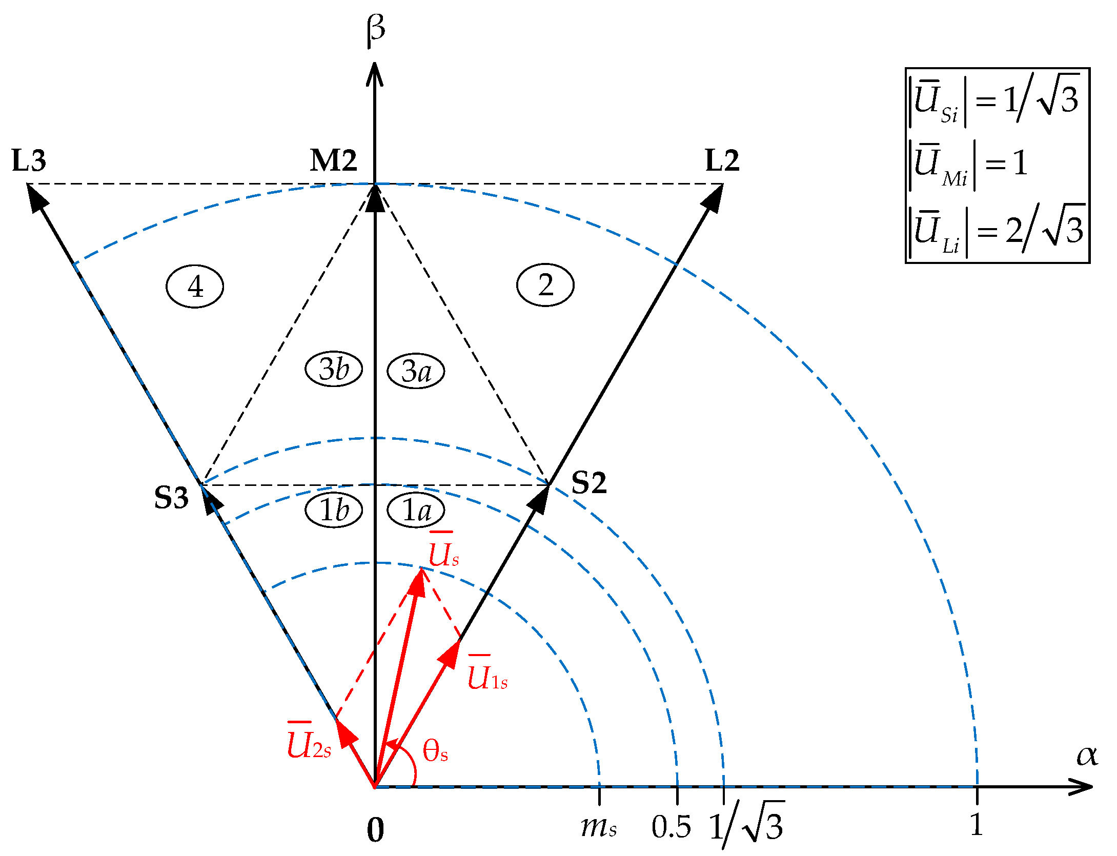
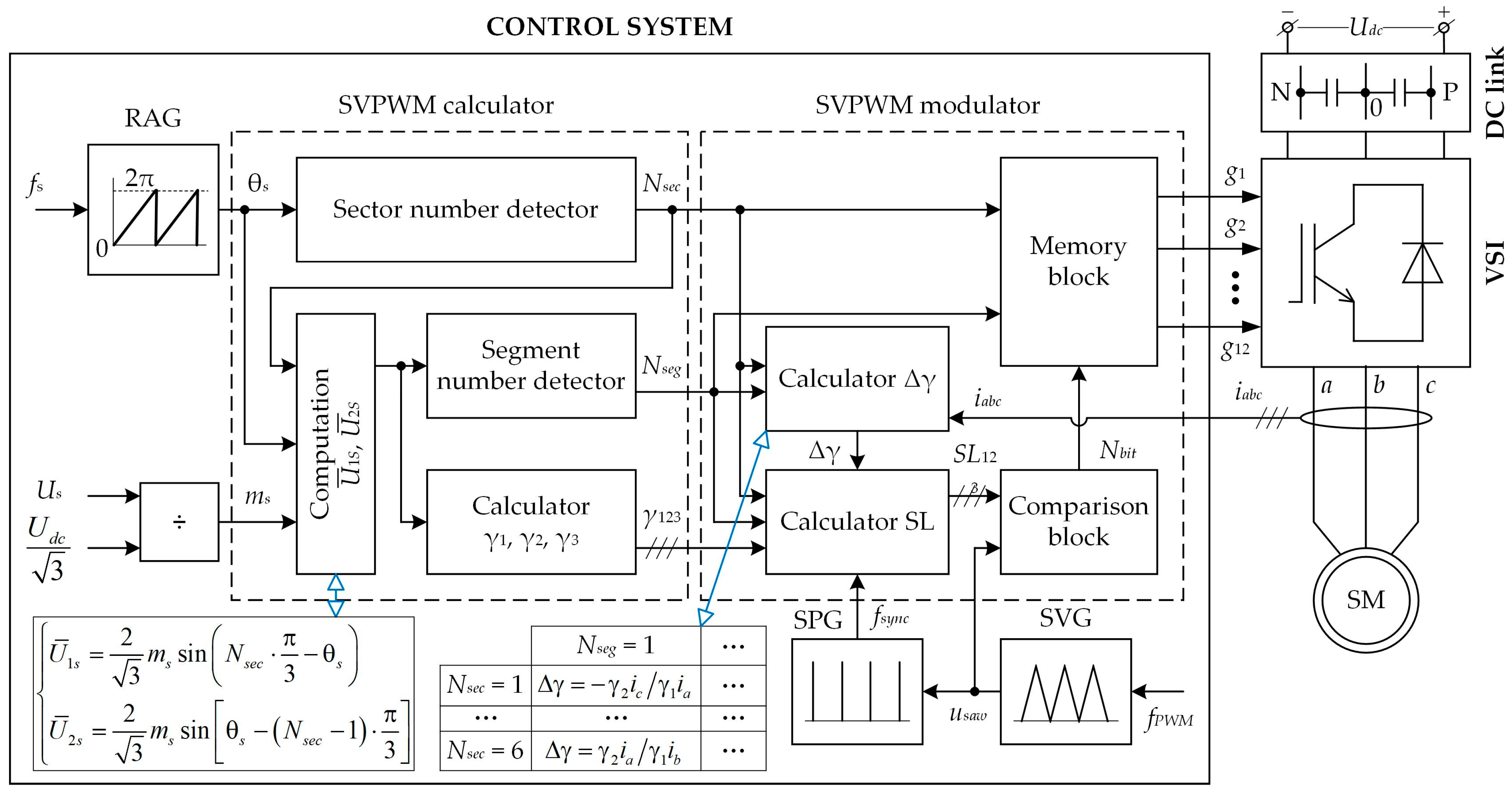
2. SVPWM Algorithm with the Base Switching Sequence for the 3L NPC VSI

The SVPWM algorithm proved itself as one of the most promising approaches to 3L NPC VSI control due to its high flexibility and applicability in a wide range of problems depending on the specific requirements of the ED system. This algorithm does not calculate instant voltage values when implemented. Instead, it calculates the moments and durations of power key activation to generate a spatial voltage vector represented by a system of three-phase voltages [16,17]
u S = 2 3 u a + u b e j 2 π 3 + u c e j 4 π 3
Based on the (1) conversion, base voltage vectors are created whose numbers are determined by the number of VSI levels. For 3L NPC VSIs, there are 19 base vectors, which correspond to 27 state combinations. These vectors form a vector diagram split into 6 sectors composed of 4 segments a. Depending on the length, these base vectors can be divided into 6 large U ¯ L 1 U ¯ L 6 ; 6 medium U ¯ M 1 U ¯ M 6 ; 6 small vectors U ¯ S 1 U ¯ S 6 , and 1 zero vector U ¯ 0 [18,19]. Small base vectors are formed from 12 combinations, 6 of which are p-type (no state [N]), while the other 6 are n-type (no state [P]).
The control parameters of the algorithm include spatial vector coordinates (module and rotation angle) set by the durations of base vector activation. Normally, the spatial vector U ¯ s is modulated based on the three nearest base vectors following the volt-second balance principle [20]. For instance, for segment 1 (sector II) (see Figure 1), vector U ¯ s can be represented as a system of equations:
U ¯ s = γ 1 U ¯ S 2 + γ 2 U ¯ S 3 + γ 3 U ¯ 0 ; γ 1 + γ 2 + γ 3 = 1 ,
where γ 1 = t 1 / T P W M ; γ 2 = t 2 / T P W M ; and γ 3 = t 3 / T P W M are relative durations of activation for base vectors U ¯ S 2 , U ¯ S 3 , and, respectively, and t1, t2, and t3 are their absolute values.
The projections of the spatial vector U ¯ s on the edges of the respective sector can be calculated using the following expressions:
U ¯ 1 s = 2 3 m s sin N sec π 3 θ s ; U ¯ 2 s = 2 3 m s sin θ s N sec 1 π 3 ,
where m s = U s U d c / 3 is the modulation factor; θs is the rotation angle of the vector U ¯ s ; and Nsec = 1…6 is the number of the sector containing the vector U ¯ s .
These expressions evaluate the projections of the spatial vector U ¯ s on sector borders in any of the four segments. Expressions (3) show that these projections depend on the modulation index ms, which affects the length of the vector U ¯ s , sector number Nsec, and current control angle θs, which changes in real time when the vector U ¯ s rotates.
The sector number and the relative duration of the nearest base vector activation duration can be determined using the expressions in Table 1.
In 3L NPC VSIs, the imbalance of voltage between the two capacitors Cd1 and Cd2 in the DC link (neutral point voltage imbalance) is one of the inevitable technical problems causing the following negative effects: (1) overvoltage on passive and active circuit elements, which may result in the reduction in their service life and even failure; (2) output voltage asymmetry causing voltage and current curve distortions on the inverter output. The authors of [21] studied the impact of base vectors on the neutral point (NP) voltage. The results of their research are presented in Table 2. It was established that in the motoring mode, large and zero base vectors do not affect the NP voltage. At the same time, in small base vectors, p-type combinations increase the NP voltage while n-type combinations result in its reduction. Average base vectors may increase or decrease the NP voltage depending on their direction and the duration of impact.
To synthesize the vector U ¯ s , whose end is in segment 1 of sector II (see Figure 1, b), we can use various versions of base vectors U ¯ S 2 , U ¯ S 3 , and U ¯ 0 :
U ¯ S = γ 1 U ¯ S 2 [ OON ] [ PPO ] + γ 2 U ¯ S 3 [ NON ] [ OPO ] + γ 3 U ¯ 0 [ PPP ] [ OOO ] [ NNN ] ; γ 1 + γ 2 + γ 3 = 1 .
From the system of Equation (4), we can obtain multiple switching sequence options due to the excessive combination of small and zero base vectors. High-power EDs require low switching frequency due to significant switching losses, which, in turn, leads to significant voltage and current curve deviations from the perfect sine form. Among the classic SS, the base SS is the most suitable one because it ensures the best voltage and current quality on the inverter output [22]. This SS uses all the excessive small and zero base vector state combinations (see Figure 2), which results in increased switching loss. The simultaneous presence of p-type and n-type combinations in the base SS helps maintain the NP voltage balance through the even distribution of their activation duration over the PWM period.
In each of the PWM periods, segment 1 requires 12 power key switching pairs, segment 3 requires 8 pairs, and segments 2 and 4 require 6 pairs. According to Figure 2, switching losses are at their highest when the modulation index ms changes within the range of 0–0.5, because, in this case, the end of the spatial vector U ¯ s is only located in segment 1. When modulation factor values are between 0.5 and 1 / 3 , the end of the vector U ¯ s passes through segments 1 and 3, which results in a reduced switching loss. When the modulation factor increases further from 1 / 3 to 1 and segment 1 is absent, the operating regions of segments 2 and 4 are expanded, and that of segment 3 is shrunk, which also results in the reduction in the switching loss.
Despite the high quality of voltage and current on the VSI output, the base SS causes the most switching losses in SVPWM. Therefore, minimizing the amount of switching while preserving acceptable electricity quality is a relevant research problem.

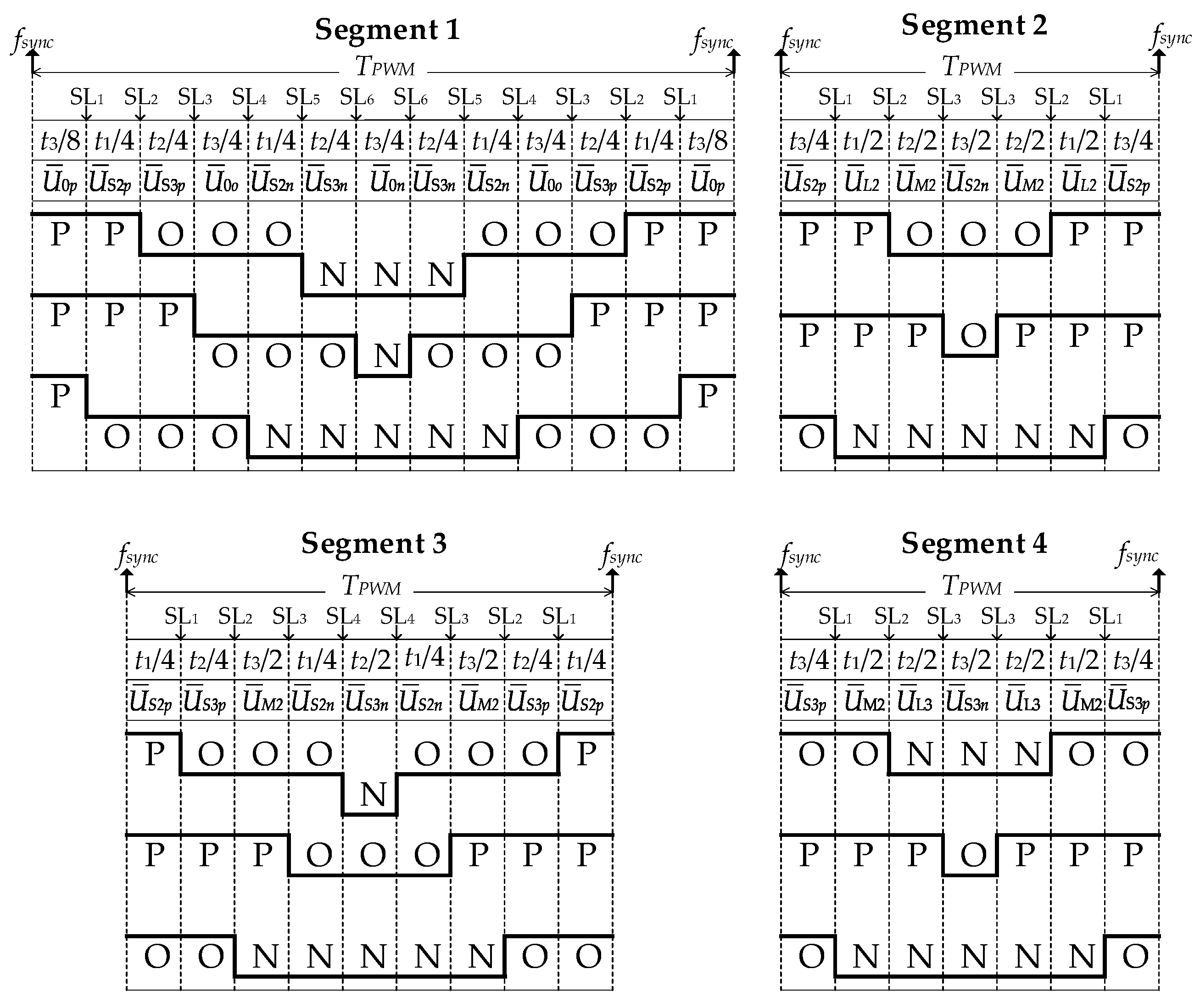
3. Improved SVPWM Algorithm with the Seven-Stage Switching Sequence for the 3L NPC VSI

This section suggests an improved SVPWM algorithm with a seven-stage SS. The key feature of a seven-stage SS is its capability to control NP voltage through the adjustment of activation duration for various types of small base vector state combinations using a specific methodology.
Figure 3 shows a seven-stage SS that performs 6 base vectors per one PWM period. Unlike the base SS, the seven-stage SS excludes combinations [PPP] and [NNN] for the zero base vector in segment 1. The NP voltage in segments 2 and 4 is controlled using only one small base vector with a total activation duration for p-type and n-type state combinations distributed evenly over one quantization period T PWM . Segments 1 and 3 simultaneously use two small base vectors, where the even distribution over the period T PWM is only provided for one vector with a longer activation duration. This vector is referred to as the dominant small base vector. For instance, if the spatial voltage vector U ¯ s is in sector II and segments 1a or 3a (Figure 1, b), then the vector U ¯ S 1 can be selected as the dominant small base vector. In segments 1b or 3b, it is the vector U ¯ S 2 . This SS requires 6 power key switching pairs for each PWM period and 2 additional pairs while transitioning to regions a and b.
Thus, a seven-stage SS can control NP voltage through the distribution of activation durations of p-type and n-type state combinations of the small base vector (for segments 2 and 4) or the dominant small base vector (for segments 1 and 3) during the PWM period. This vector is referred to as the distributed base vector, and its relative duration for p-type and n-type states can be determined using the following expression [17]:
γ j p = γ j 2 1 + Δ γ ; γ j n = γ j 2 1 Δ γ ,
where Δγ is the control range of relative durations for p-type and n-type state combinations of the distributed vector over one PWM period that can change over the range 1 Δ γ 1 ; j = 1…3 is the relative duration index of the distributed vector.
Over a PWM period, the average value of the NP current i ¯ N P generated by base vectors in the seven-stage SS can be determined with the following expression:
i ¯ N P = γ k i N P . k ,
where k is the relative duration index for state combinations of base vectors in the selected seven-stage SS; iNP.k is the NP current generated by the combination of base vector states with index k.
For the mathematical description of the inverter, the three states of the x-phase of the inverter [N], [O], [P] can be recorded using logical signals s x = 1 ;   0 ;   1 . In this case, the output phase voltage u x can be expressed as a function of power key states and the condenser u d 1 and u d 2 voltages [18]:
u x = u C d 2 F d 2 x 1 3 m = a b , c F d 2 m u C d 1 F d 1 x 1 3 m = a b , c F d 1 m ; u C d 1 + u C d 2 = U d c .
Here, F d 2 x and F d 1 x are the functions of the x-phase state determining the state of connection between the DC link and each phase calculated using the following expressions:
F d 2 x = s x s x + 1 / 2 ; F d 1 x = s x s x 1 / 2 .
The NP voltage deviation inevitably results in neutral point current iNP determined depending on the state functions and inverter output phase currents:
i N P = x a , b , c F d 2 x + F d 1 x i x = x a , b , c s x 2 i x ,
where ix is the phase load current (x—phase a, b, and c).
We can insert the logical states of base vectors in the expression above to achieve the neutral point current definition. For instance, see vector U ¯ S 2 n [OON]:
i NP = x a , b , c s x 2 i x = s a 2 i a + s b 2 i b + s c 2 i c = 0 2 i a + 0 2 i b + 1 2 i c = i c .
Using the Laplace transform, we obtain the deviation of the NP voltage as follows, according to the current direction,
i C d 1 i C d 2 = i N P ; u C d 1 + u C d 1 = u d c ; u C d 1 = 1 C d 1 i C d 1 d t ; u C d 2 = 1 C d 2 i C d 2 d t .
Using the Laplace transform, we obtain the following:
I ˙ C d 1 I ˙ C d 2 = I ˙ N P ; U ˙ C d 1 + U ˙ C d 1 = U ˙ d c ; U ˙ C d 1 = I ˙ C d 1 s C d 1 ; U ˙ C d 2 = I ˙ C d 2 s C d 2 .
Solving this system of equations, we obtain the following:
U ˙ C d 1 = C d 2 C d 1 + C d 2 U ˙ d c + 1 C d 1 + C d 2 I ˙ N P s ; U ˙ C d 2 = C d 1 C d 1 + C d 2 U ˙ d c 1 C d 1 + C d 2 I ˙ N P s .
Thus,
Δ U ˙ N P = U ˙ C d 1 U ˙ C d 2 = C d 2 C d 1 C d 1 + C d 2 U ˙ d c + 2 C d 1 + C d 2 I ˙ N P s .
Based on the reverse Laplace transform, we obtain the following:
Δ u N P = u C d 1 u C d 2 = C d 2 C d 1 C d 2 + C d 1 U d c + 2 C d 2 + C d 1 i N P d t .
Expression (15) shows that, apart from factors associated with the hardware side (Udc, Cd1, Cd2), NP voltage deviation is also affected by the NP current generated by base vectors (through the value of sx) and the load (phase current ix) following Expression (9). As mentioned before, the NP voltage imbalance causes voltage and current curve distortion on the inverter output. Therefore, minimizing the NP voltage deviations helps improve the quality of electric power conversion. This can be achieved by adjusting the average value of the NP current to zero using the Δγ value (see Formulas (6) and (5)).
The results for the equation i ¯ N P = 0 are provided in Table 3, and they help determine the Δγ values that are integrated with the VSI control system.
The block diagram of the improved SVPWM algorithm with the seven-stage SS for the 3L NPC VSI is shown in Figure 4. The control system adjusts the inverter voltage and frequency through the set parameters Us and fs. The system includes several key functional blocks: rotation angle generator (RAG), sawtooth voltage generator (SVG), synchronizing pulse generator (SPG), SVPWM computer, and SVPWM modulator.
The RAG block is an integrator calculating the rotation angle θ for the spatial vector of voltage U ¯ s .
The SVG generates symmetrical sawtooth voltage usaw with the PWM frequency fPWM.
The SPG generates synchronizing pulses fsync when the signal usaw crosses the zero level.
The SVPWM modulator generates 12 logical control signals for inverter power keys and is composed of the following blocks: Δγ computer, switching level (SL) computer, comparison block, and memory block.
The Δγ computer calculates the value of Δγ following Table 3 using phase load currents ia, ib, and ic to minimize the NP voltage deviation.
The SL computer calculates three SLs depending on the position of the end of the spatial voltage vector U ¯ s .
The comparison block compares the sawtooth voltage usaw and the SL to determine the torques when base vectors are activated in each PWM period. The output data are coded with a two-bit code Nbit containing the information on the address of the memory cell that stores the information about the activation of a specific base vector.
The memory block stores the information on the power key activation state codes depending on the sector number Nsec and the segment number Nseg, as well as the binary code Nbit.

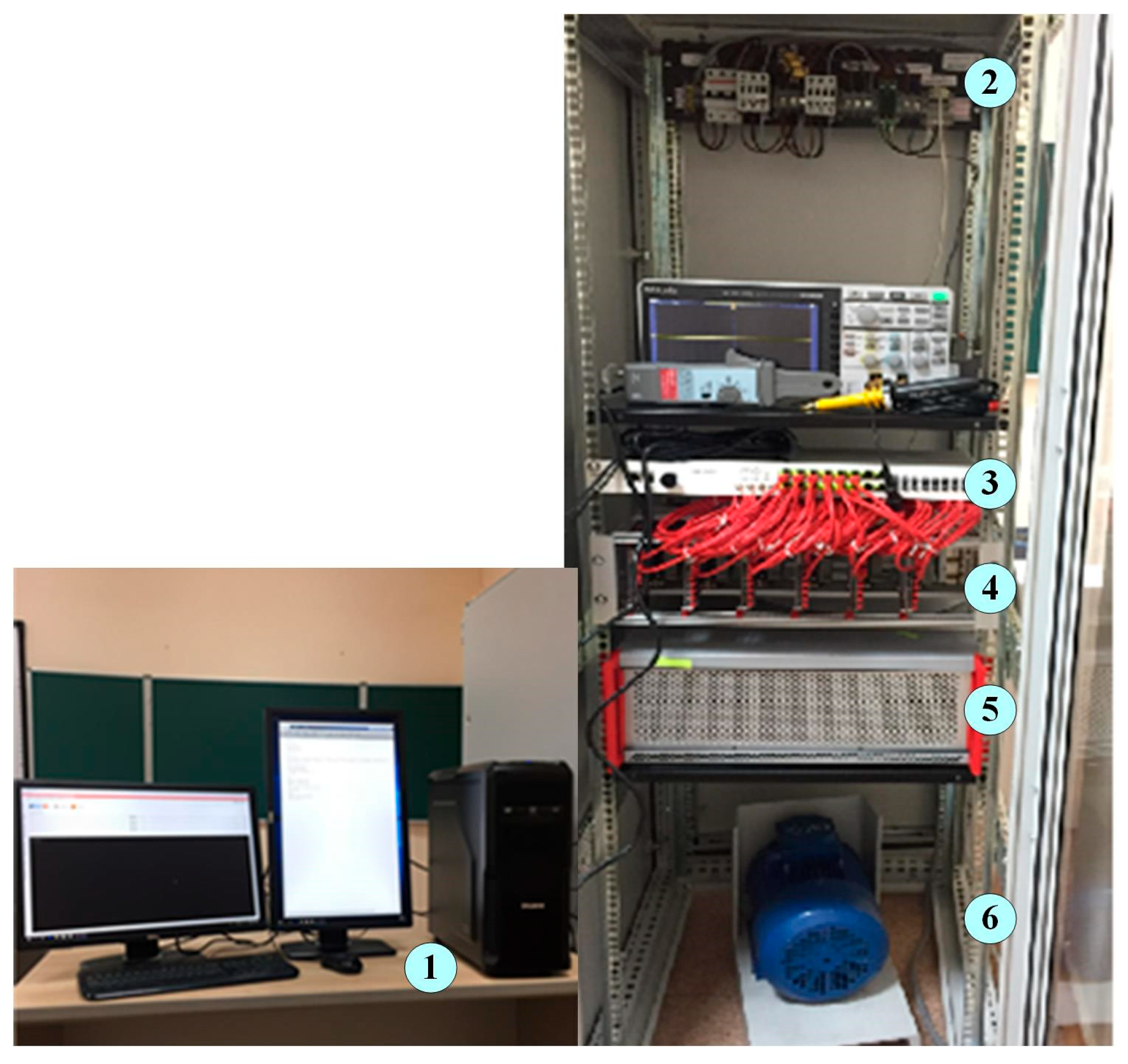
4. Experimental Research of the Improved SVPWM Algorithm with a Seven-Stage Switching Sequence

To test the efficiency of the improved SVPWM algorithm with a seven-stage SS (see Figure 4), we used a three-level power converter laboratory setup from Imperix Ltd (1950 Sion, Switzerland). This setup includes (Figure 5) a personal computer (1), filters (5) for 380 V three-phase AC grid connection (2), three integral semiconductor racks with NPC based on IGBT modules Vincotech P924F33, (4), a BoomBox control platform (3), and a 4 kW asynchronous motor (AM) (6).
We used specialized program blocks from the Imperix Blockset library in Matlab/Simulink 2017b to program three SVPWM algorithms featuring base SS (see Section 2), classic seven-stage SS (see Figure 4 with Δγ = 0), and an improved algorithm with a seven-stage SS (see Figure 4, Δγ ≠ 0). In all algorithms, voltage and frequency were controlled following U/f = const with a voltage boost in the low-frequency area of 5% of the nominal AM stator voltage.
After that, the program codes of algorithms were compiled in C/C++ and integrated with the BoomBox platform via a JTAG emulator. We used a USB connector to connect to the BoomBox Control and software platform to obtain a graphic representation and manage the data loaded from Matlab/Simulink 2017b to the TMS320C28346 central signal processor of the BoomBox control platform during the first stage. BoomBox RCP is a Rapid Control Prototyping (RCP) platform based on the TMS320C28346 digital signal processor (DSP) and the Xilinx XC9536XL-10VQG44C field programmable logic device (FPLD). It ensures the flexibility of programming and supports the implementation of even the most complex control algorithms. The BoomBox platform also supports real-time monitoring and debugging. Phase currents and voltages were measured and displayed at a sampling rate of 50 usec. The obtained data were imported into Matlab/Simulink 2017b for further analysis. The key laboratory setup parameters are presented in Table 4.
Figure 6 shows the instant voltage values on the two capacities in the DC link at a normalized set frequency of f*s = 0.8 and nominal motor load for SVPWM algorithms with a base and classic seven-stage SS (Δγ = 0) and the improved SVPWM algorithm with a seven-stage SS [23,24]. Here, the normalized set frequency is calculated using the following formula:
f s * = f s f s . r .
where fs.r = 50 Hz is the rated AM stator frequency.
When the DC link voltage is 540 V and the NP voltage balance is perfect, the voltage on each capacitor is 270 V (red curve; see Figure 6). However, as mentioned before, the NP voltage inevitably becomes unbalanced during the operation of the 3L NPC VSI. Unlike the SVPWM algorithms with the base SS and the classic seven-stage SS, the improved SVPWM algorithm can reduce the maximum NP voltage deviation by 40% and 52.6%, respectively. This helps improve the shape of the inverter output current (Figure 7). Unlike the established SVPWM algorithms, odd harmonic components of the orders 43–57 in the suggested algorithm increase insignificantly in the phase output current spectrum. Simultaneously, lower-frequency 5th-order harmonics are reduced from 1.5% and 1.8% to 0.65%, while the 7th-order harmonics are reduced from 1.8% and 1.95% to 0.75%. As a result, the THD current distortion factor is reduced from 2.83% and 3.25% to 2.66%.
The complex efficiency assessment of the improved SVPWM algorithm with a seven-stage SS used the following parameters:
-
The number of power key switching pairs per one period of the fundamental harmonic on the output of the inverter Nsw;
-
The maximum relative NP voltage deviation,
δ u N P . m = Δ u N P . m U d c 100 % = u C d 1 u C d 2 max U d c 100 % ,
where uCd1 and uCd2 are voltages on capacitors Cd1 and Cd2 in the VSI DC link and Udc is the constant inverter power voltage;
-
The total harmonic distortion factor (THD) of the inverter output current,
K i = n = 2 I m ( n ) 2 I m ( 1 ) 100 % ,
where Im(1), Im(n) is the amplitude of the first (fundamental) harmonic and harmonic n;
-
The distortion factors of 5th and 7th harmonics (Ki(5) and Ki(7)) in the inverter output current spectrum
K i ( 5 ) = I m ( 5 ) I m ( 1 ) 100 % ; K i ( 7 ) = I m ( 7 ) I m ( 1 ) 100 %
Figure 8 and Figure 9 show the experimental dependencies between the number of power key switching pairs Nsw per one period of the fundamental harmonic on the inverter output, the relative NP voltage error δuNP.m, and harmonic current distortion factors Ki, Ki(5), and Ki(7), depending on the normalized set frequency f*s, and their average values N ¯ s w , δ u ¯ N P . m , K ¯ i , K ¯ i ( 5 ) , and K ¯ i ( 7 ) over the entire range of frequency f*s (0 to 1.0) for the three SVPWM algorithms: with the base SS, the classic seven-stage SS, and the improved SVPWM algorithm with a seven-stage SS.
The analysis of dependencies shown in Figure 8 and their average values (Figure 9) allows us to draw the following conclusions:
-
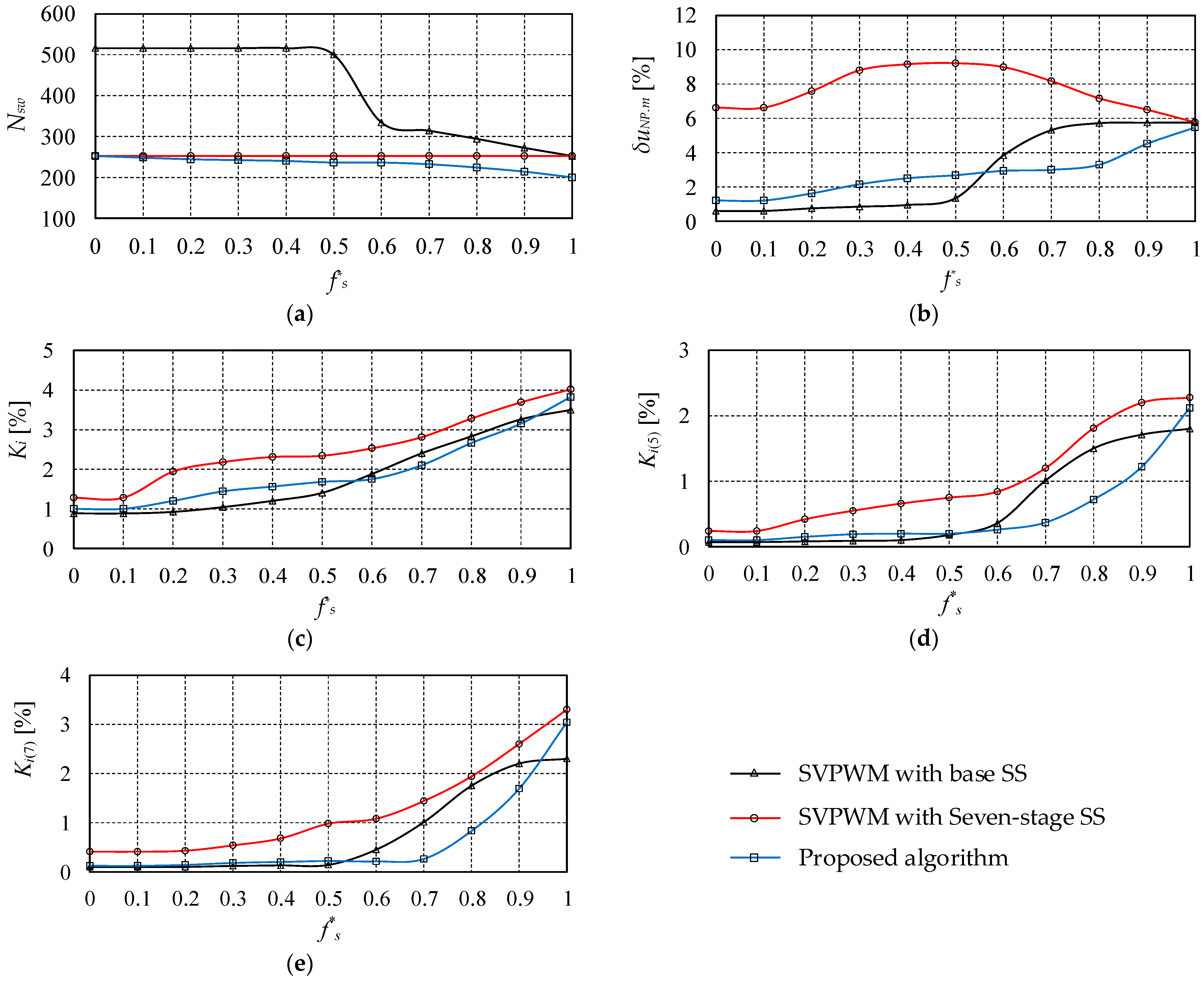
The improved SVPWM algorithm with a seven-stage SS has the least number of power key switching pairs Nsw over the entire range of frequency f*s compared to the established algorithms (see Figure 9, a). For instance, compared to the SVPWM algorithm with the base SS, the suggested algorithm significantly reduces the number of power key switchings by about 51.5%, especially in the range of frequency f*s from 0 to 0.5. This can be attributed to the significant excess of base vector switching in each PWM period in the base SS (see Figure 2, segment 1). The average switching value N ¯ s w over the range of frequency f*s, in this case, is reduced from 414 to 234 pairs, which corresponds to a 43.48% reduction (see Figure 9). Compared to the algorithm with the classic seven-stage SS, the improved SVPWM algorithm may also reduce the average number of switchings N ¯ s w from 252 to 234 pairs (see Figure 9), which is equivalent to a 7.14% reduction. This can be attributed to the increase in factor Δγ to the maximum value of ±1.0, which results in the reduction in switching levels in each PWM period.
-
The SVPWM algorithm with the base SS minimizes the impact of small base vectors on the NP voltage due to the even distribution of activation durations of p-type and n-type small base vectors but it does not account for the impact of medium vectors used in segments 2, 3, and 4 (see Figure 2). Because of this, factor δuNP.m is at the minimum at frequency f*s between 0 and 0.5, but it increases dramatically when f*s is in the range of 0.5 and 1, reaching the maximum of 5.8% at f*s = 1 (see Figure 9, b).

5. Analysis and Discussion

-
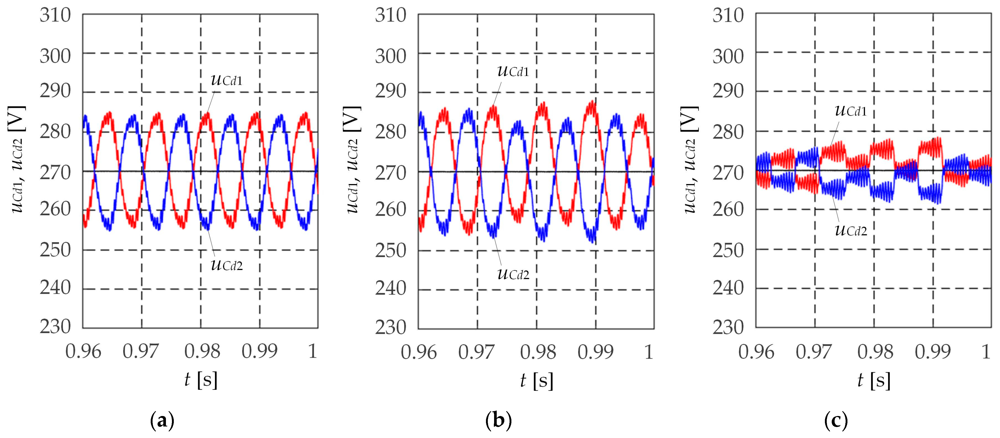
The SVPWM algorithm with the classic seven-stage SS (Δγ = 0), used as the basis for the development of the improved algorithm, does not support NP voltage control. This results in a high level of deviation δuNP.m, reaching a maximum value of δuNP.m = 9.2% at f*s = 0.5 (see Figure 8, b), when the activation duration of small base vectors in each PWM period reaches the highest value.
-
The improved SVPWM algorithm with a seven-stage SS provides the best NP voltage control among the considered algorithms by controlling the duty factor Δγ of distributed base vectors in each PWM period based on phase load currents. Thus, the average value of error δ u ¯ N P over the entire range of frequency f*s for the improved SVPWM algorithm is 2.74% (see Figure 9), which is 64.4% lower than for the SVPWM with the classic seven-stage SS (δuNP = 7.69%) and 4.2% lower than for the SVPWM with the base SS (δuNP = 2.86%).
-
In the frequency range f*s of 0 to 0.5, the value of deviation δuNP.m for the improved SVPWM algorithm is slightly higher than for the established SVPWM algorithm with the base SS (see Figure 8, b), because, in this range, NP voltage in the suggested algorithm is only controlled with a single dominant small base vector while the second small base vector remains uncontrolled. When f*s > 0.5, deviation δuNP.m in the improved SVPWM algorithm becomes smaller than in the established SVPWM algorithm with the base SS, which can be explained by the heavy influence of medium base vectors in the established algorithm.
-
When f*s > 0.8, errors δuNP.m in the improved SVPWM algorithm increase significantly and reach 5.1% at f*s = 1 (see Figure 8, b), like in the established SVPWM algorithm with the base SS. This can be explained by the fact that this region has significantly shorter small base vector activation durations, which restricts the NP voltage balance control in the suggested algorithm. To reduce this error, we suggest increasing either the capacity of condensers Cd1 and Cd2 of the inverter DC link or the frequency of PWM. The first option is preferred as it only leads to an increase in the inverter’s price, weight, and dimensions, while in the other case, the efficiency of the converter drops due to the increased switching loss.
-
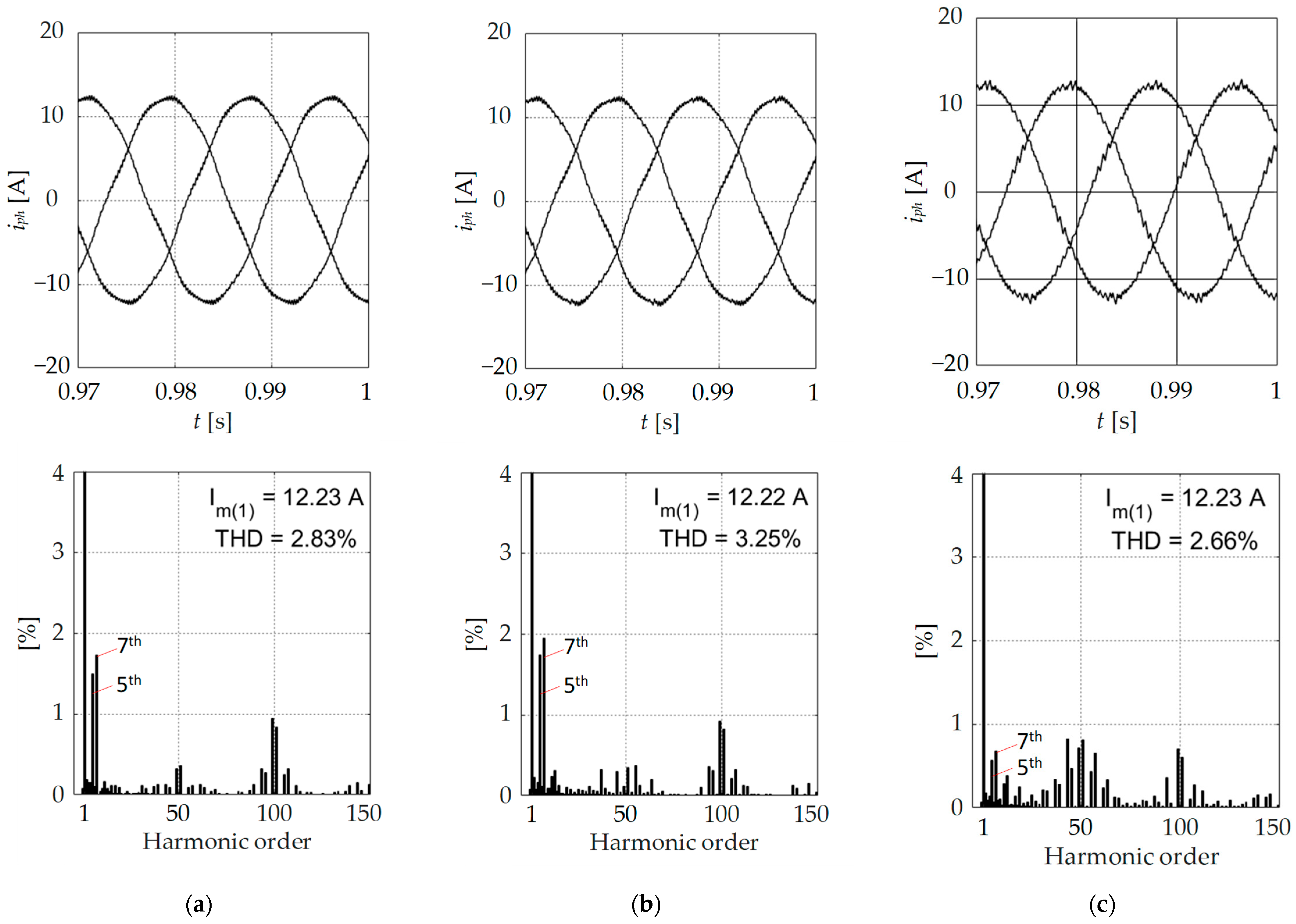
The total current distortion factor Ki for all of the considered algorithms (see Figure 8, c) directly depends on the NP voltage error δuNP.m and is similar to the dependencies shown in Figure 8, b. This can be attributed to the fact that the NP voltage imbalance leads to voltage asymmetry in capacitors Cd1 and Cd2 of the DC link and, as a result, causes voltage and current curve distortions on the inverter output.
-
In terms of the average total current distortion factor K ¯ i , the suggested SVPWM algorithm only loses 0.1% of the absolute value across the entire frequency range f*s compared to the established SVPWM algorithm with the base SS (see Figure 9), but its average values of low-frequency current harmonic factors K ¯ i ( 5 ) and K ¯ i ( 7 ) are 19% and 15.7% better, respectively. Note that the odd low-frequency harmonics (5, 7, …) have the greatest negative impact and may lead to increased magnetic core losses and reduced motor efficiency, increased losses in windings causing motor overheating and service life reduction, and disruptions in the evenness of the rotating magnetic field of the motor, which leads to increased vibration and noise levels.

6. Conclusions

This article demonstrates an improved SVPWM algorithm with a seven-stage switching sequence for 3L NPC VSIs. The proposed algorithm calculates relative durations for p-type and n-type state combinations using the load phase currents. The suggested SVPWM provides the lowest loss, as well as the best NP voltage balance among the established algorithms, while preserving the quality of the inverter output current comparable to the established SVPWM algorithm with the base SS. The obtained results confirm the efficiency of the suggested algorithm and its great potential for power converters in industry.

Author Contributions

Conceptualization, A.N.S.; methodology, V.K.L.; software, V.K.L.; validation, A.S.M.; formal analysis, A.N.S.; investigation, V.K.L.; resources, A.S.M.; data curation, A.S.M.; writing—original draft preparation, V.K.L.; writing—review and editing, M.M.D. and A.A.R.; visualization, V.S.B.; supervision, A.N.S.; project administration, A.N.S. All authors have read and agreed to the published version of the manuscript.

Funding

This work was financially supported by the Moscow Polytechnic University within the framework of the grant named after Pyotr Kapitsa.

Institutional Review Board Statement

Not applicable.

Informed Consent Statement

Not applicable.

Data Availability Statement

The original contributions presented in this study are included in the article. Further inquiries can be directed to the corresponding author(s).

Conflicts of Interest

The authors declare no conflicts of interest.

Nomenclature

PWMPulse-width modulation
SVPWMSpace vector PWM
EDElectric drive
3LThree-level
VSIVoltage source inverter
NPCNeutral point clamped
FCFrequency converter
SSSwitching sequence
NPNeutral point
RAGRotation angle generator
SVGSawtooth voltage generator
SPGSynchronizing pulse generator
THDTotal harmonic distortion

References

  1. Luna, M. High-Efficiency and High-Performance Power Electronics for Power Grids and Electrical Drives. Energies 2022, 15, 5844. [Google Scholar] [CrossRef]
  2. Shahane, R.; Rao, K.N.; Shukla, A. A Review on Hybrid Modular Multilevel Converters for Medium Voltage Applications. In Proceedings of the IEEE Energy Conversion Congress and Exposition (ECCE), Detroit, MI, USA, 9–13 October 2022; pp. 1–8. [Google Scholar] [CrossRef]
  3. Nabae, A.; Takahashi, I.; Akagi, H. A New Neutral-Point-Clamped PWM Inverter. IEEE Trans. Ind. Appl. 1981, IA-17, 518–523. [Google Scholar] [CrossRef]
  4. Kumara, R.; Singh, B. Performance Improvements of Power Converters for High Power Induction Motor Drive. E-Prime-Adv. Electr. Eng. Electron. Energy 2023, 5, 100214. [Google Scholar] [CrossRef]
  5. Sommer, R.; Mertens, A.; Brunotte, C.; Trauth, G. Medium voltage drive system with NPC three-level inverter using IGBTs. In Proceedings of the IEE Seminar PWM Medium Voltage Drives (Ref. No. 2000/063), Birmingham, UK, 11 May 2000; pp. 3/1–3/3. [Google Scholar] [CrossRef]
  6. Mishra, M.K.; Joshi, A.; Ghosh, A. Control Schemes for Equalization of Capacitor Voltages in Neutral Clamped Shunt Compensator. IEEE Trans. Power Deliv. 2003, 18, 538–544. [Google Scholar] [CrossRef]
  7. Lee, D.H.; Lee, S.R.; Lee, F.C. An Analysis of Midpoint Balance for the Neutral-Point-Clamped Three-Level VSI. In Proceedings of the PESC 98 Record. 29th Annual IEEE Power Electronics Specialists Conference (Cat. No.98CH36196), Fukuoka, Japan, 22 May 1998; pp. 193–199. [Google Scholar] [CrossRef]
  8. Behera, S.; Behera, M.K.; Majhi, H.; Akram, F. Study of PWM Control Techniques for Single Phase Inverter with Variable DC Input. In Proceedings of the Second International Conference on Intelligent Computing and Control Systems (ICICCS), Madurai, India, 14–15 June 2018; pp. 811–816. [Google Scholar] [CrossRef]
  9. Chen, F.; Qiao, W. A General Space Vector PWM Scheme for Multilevel Inverters. In Proceedings of the IEEE Energy Conversion Congress and Exposition (ECCE), Milwaukee, WI, USA, 18–22 September 2016. [Google Scholar] [CrossRef]
  10. Pou, J.; Zaragoza, J.; Ceballos, S.; Saeedifard, M.; Boroyevich, D. A Carrier-Based PWM Strategy with Zero-Sequence Voltage Injection for a Three-Level Neutral-Point-Clamped Converter. IEEE Trans. Power Electron. 2012, 27, 642–651. [Google Scholar] [CrossRef]
  11. Jiang, W.; Huang, X.; Wang, J.; Wang, J.; Li, J. A Carrier-Based PWM Strategy Providing Neutral-Point Voltage Oscillation Elimination for Multi-Phase Neutral Point Clamped 3-Level Inverter. IEEE Access 2019, 7, 124066–124076. [Google Scholar] [CrossRef]
  12. Xiang, C.Q.; Shu, C.; Han, D.; Mao, B.K.; Wu, X.; Yu, T.J. Improved Virtual Space Vector Modulation for Three-Level Neutral-Point-Clamped Converter with Feedback of Neutral-Point Voltage. IEEE Trans. Power Electron. 2017, 33, 5452–5464. [Google Scholar] [CrossRef]
  13. Bhalodi, K.H.; Agrawal, P. Space Vector Modulation with DC-Link Voltage Balancing Control for Three-Level Inverters. In Proceedings of the International Conference on Power Electronic, Drives and Energy Systems, New Delhi, India, 12–15 December 2006. [Google Scholar] [CrossRef]
  14. Lewicki, A.; Krzeminski, Z.; Abu-Rub, H. Space-Vector Pulsewidth Modulation for Three-Level NPC Converter with the Neutral Point Voltage Control. IEEE Trans. Ind. Electron. 2011, 58, 5076–5086. [Google Scholar] [CrossRef]
  15. Dhasharatha, G.; Varma, N.R.; Spandana, A.; Kumar, P.A.; Venumadhav, B.; Kumar, B.P. Design and Implementation of Three-phase Three Level NPC Inverter. In Proceedings of the 7th International Conference on Trends in Electronics and Informatics (ICOEI), Tirunelveli, India, 11–13 April 2023; pp. 106–110. [Google Scholar] [CrossRef]
  16. Nandhini, E.; Sivaprakasam, A. A Review of Various Control Strategies Based on Space Vector Pulse Width Modulation for the Voltage Source Inverter. IETE J. Res. 2022, 68, 3187–3201. [Google Scholar] [CrossRef]
  17. Wu, B.; Narimani, M. High-Power Converters and AC Drives, 2nd ed.; Wiley-IEEE Press: Hoboken, NJ, USA, 2017. [Google Scholar]
  18. Shishkov, A.N.; Dudkin, M.M.; Le, V.K.; Eremin, N.A. Optimizing DC Link Capacitors in Three-Level Voltage Inverter Based on Space-Vector PWM with Seven-Stage Switching Sequence. In Proceedings of the International Russian Smart Industry Conference (SmartIndustryCon), Sochi, Russia, 25–29 March 2024; pp. 949–956. [Google Scholar] [CrossRef]
  19. Sun, G.; He, Y.; Du, H.; Zhuang, S.; Liu, J. The Equivalent Relationship Between Space Vector Modulation and Carrier Modulation of Parallel NPC-3L Inverters. IEEE J. Emerg. Sel. Top. Power Electron. 2023, 12, 731–742. [Google Scholar] [CrossRef]
  20. Busquets-Monge, S.; Bordonau, J.; Boroyevich, D.; Somavilla, S. The Nearest Three Virtual Space Vector PWM—A Modulation for the Comprehensive Neutral-Point Balancing in the Three-Level NPC Inverter. IEEE Power Electron. Lett. 2004, 2, 11–15. [Google Scholar] [CrossRef]
  21. Dudkin, M.M.; Shishkov, A.N.; Le, V.K. An Algorithm for a Space-Vector Pulse Width Modulation with a Hybrid Switching Sequence for a Three-Level Neutral Point Clamped Voltage Source Inverter. Power Syst. Technol. 2024, 48, 55–84. [Google Scholar] [CrossRef]
  22. Shishkov, A.N.; Dudkin, M.M.; Le, V.K.; Eremin, N.A. The Influence of Different Types of Switching Sequences in Space-Vector PWM on Output Characteristics of Three-Level Voltage Inverter. In Proceedings of the International Ural Conference on Electrical Power Engineering (UralCon), Magnitogorsk, Russia, 29 September–1 October 2023; pp. 690–696. [Google Scholar] [CrossRef]
  23. Imperix Ltd. B-Box RCP3.0 Rapid Prototyping Controller User Manual; Imperix Ltd.: Sion, Switzerland, 2025; p. 17. Available online: https://cdn.imperix.com/wp-content/uploads/document/B-Box_Datasheet.pdf (accessed on 20 February 2025).
  24. Shishkov, A.N.; Dudkin, M.M.; Le, V.K.; Eremin, N.A. Neutral Point Voltage Balance Based on Space-Vector PWM with Five-Stage Sequence for Three-Level Voltage Inverter. In Proceedings of the International Russian Smart Industry Conference (SmartIndustryCon), Sochi, Russia, 27–31 March 2023; pp. 586–592. [Google Scholar] [CrossRef]
Figure 1. Vector diagram for sector II.
Energies 18 02452 g001
Figure 2. Base SS for sector II.
Energies 18 02452 g002
Figure 3. Seven-stage SS for Sector II.
Energies 18 02452 g003
Figure 4. Block diagram of the improved SVPWM algorithm with the seven-stage SS for the 3L NPC VSI.
Energies 18 02452 g004
Figure 5. Overview of the three-level power converter laboratory setup (1. Windows and Matlab/Simulink 2017b (Imperix Blockset); 2. AC grid; 3. B-Box control platform; 4. 3L NPC FC; 5. filters; 6. asynchronous motor 4 kW, 380 V, 50 Hz).
Energies 18 02452 g005
Figure 6. Instant voltage values on DC-link capacitors for SVPWM algorithms with the base SS (a), classic seven-stage SS (b), and the suggested SVPWM with a seven-stage SS (c) at frequency f*s = 0.8 and nominal motor load.
Energies 18 02452 g006
Figure 7. Instant motor current values and their spectral analysis for SVPWM algorithms with the base SS (a), classic seven-stage SS (b), and the suggested SVPWM with a seven-stage SS (c) at frequency f*s = 0.8 and motor load rate.
Energies 18 02452 g007
Figure 8. Experimental dependencies: the number of power key switching pairs Nsw per one period of the fundamental harmonic on the inverter output (a); relative NP voltage error δuNP.m (b); and harmonic current distortion factors Ki (c), Ki(5) (d), and Ki(7) (e) depending on the normalized set frequency f*s for the three SVPWM algorithms.
Energies 18 02452 g008
Figure 9. Average values N ¯ s w , δ u ¯ N P , K ¯ i , K ¯ i ( 5 ) , and K ¯ i ( 7 ) over the entire range of frequency f*s (0 to 1.0) for the three SVPWM algorithms.
Energies 18 02452 g009
Table 1. Determining relative durations γ1, γ2, γ3, and the segment number.
SegmentNseg = 1Nseg = 2Nseg = 3Nseg = 4
Condition U ¯ 1 s 1 / 3 ; U ¯ 2 s 1 / 3 ; U ¯ 1 s + U ¯ 2 s 1 / 3 . U ¯ 1 s > 1 / 3 U ¯ 1 s 1 / 3 ; U ¯ 2 s 1 / 3 ; U ¯ 1 s + U ¯ 2 s > 1 / 3 . U ¯ 2 s > 1 / 3
Values
γ1, γ2, γ3
γ 1 = 3 U ¯ 1 s ; γ 2 = 3 U ¯ 2 s ; γ 3 = 1 γ 1 γ 2 . γ 1 = 3 U ¯ 1 s 1 ; γ 2 = 3 U ¯ 2 s ; γ 3 = 1 γ 1 γ 2 . γ 1 = 1 3 U ¯ 2 s ; γ 2 = 1 3 U ¯ 1 s ; γ 3 = 1 γ 1 γ 2 . γ 1 = 3 U ¯ 1 s ; γ 2 = 3 U ¯ 2 s 1 ; γ 3 = 1 γ 1 γ 2 .
Table 2. Impact of base vectors on NP voltage.
Base VectorZeroLarge Medium Small
p-TypeN-Type
Switching state[PPP],
[OOO],
[NNN]
[PNN], [PPN],
[NPN], [NPP],
[NNP], [PNP]
[PON], [OPN],
[NPO], [NOP],
[ONP], [PNO]
[POO], [PPO],
[OPO], [OPP],
[OOP], [POP]
[ONN], [OON],
[NON], [NOO],
[NNO], [ONO]
NP current i N P = 0 i N P = 0 i N P 0 i N P > 0 i N P < 0
NP voltageunchanged unchanged increased/decreasedincreased decreased
Table 3. Values of Δγ for segments and sectors.
Position
U ¯ S
Segment
1a
Segment
1b
Segment
2
Segment
3a
Segment
3b
Segment
4
Sector I γ 2 i c γ 1 i a γ 1 i a γ 2 i c γ 2 i b γ 3 i a γ 3 i b γ 2 i c γ 1 i a γ 3 i b γ 1 i a γ 2 i c γ 1 i b γ 3 i c
Sector II γ 2 i b γ 1 i c γ 1 i c γ 2 i b γ 2 i a γ 3 i c γ 3 i a γ 2 i b γ 1 i c γ 3 i a γ 1 i c γ 2 i b γ 1 i a γ 3 i b
Sector III γ 2 i a γ 1 i b γ 1 i b γ 2 i a γ 2 i c γ 3 i b γ 3 i c γ 2 i a γ 1 i b γ 3 i c γ 1 i b γ 2 i a γ 1 i c γ 3 i a
Sector IV γ 2 i c γ 1 i a γ 1 i a γ 2 i c γ 2 i b γ 3 i a γ 3 i b γ 2 i c γ 1 i a γ 3 i b γ 1 i a γ 2 i c γ 1 i b γ 3 i c
Sector V γ 2 i b γ 1 i c γ 1 i c γ 2 i b γ 2 i a γ 3 i c γ 3 i a γ 2 i b γ 1 i c γ 3 i a γ 1 i c γ 2 i b γ 1 i a γ 3 i b
Sector VI γ 2 i a γ 1 i b γ 1 i b γ 2 i a γ 2 i c γ 3 i b γ 3 i c γ 2 i a γ 1 i b γ 3 i c γ 1 i b γ 2 i a γ 1 i c γ 3 i a
Table 4. Key parameters of the three-level power converter laboratory setup.
Technical ParametersValue
VSIDC-link voltage, Udc540 V
DC-link capacitor capacity, Cd1 = Cd2517 uF
P924F33 Vincotech IGBT modules600 V, 30 A, 50 kHz
LEM HLSR 20-P/SP33 current probes±20 A; bandwidth 450 kHz; measurement error ± 0.5%
Avago ACPL-C87B voltage probesbandwidth 25 kHz; measurement error ± 0.1%
FPGAXilinx XC9536XL-10VQG44C
TMS320C28346300 MHz, 256 MB NOR flash memory, 2 MB RAM, and 300 MIPS
SVPWM, fPWM2000 Hz
Control methodU/f = const
AMRate power, Pr4 kW
Linear voltage, Ul.380 V
Rate stator current, Is8.6 A
Rate frequency, fs.r50 Hz
Disclaimer/Publisher’s Note: The statements, opinions and data contained in all publications are solely those of the individual author(s) and contributor(s) and not of MDPI and/or the editor(s). MDPI and/or the editor(s) disclaim responsibility for any injury to people or property resulting from any ideas, methods, instructions or products referred to in the content.

