Article

A Simple Thermoelectrical Surface Approach for Numerically Studying Dry Band Formation on Polluted Insulators

UQAC/CENGIVRE International Research Center on Atmospheric Icing and Electrical Network Engineering, University of Quebec at Chicoutimi, 555 Boulevard de l’Université, Chicoutimi, QC G7H 2B1, Canada
*
Author to whom correspondence should be addressed.
Energies 2025, 18(10), 2412; https://doi.org/10.3390/en18102412
Submission received: 27 March 2025 / Revised: 29 April 2025 / Accepted: 6 May 2025 / Published: 8 May 2025

Abstract

:
This paper presents a simple thermoelectrical temporal surface method for numerically studying the appearance of a dry band on a polluted insulator. The proposed method combines an empirical expression of the pollution layer surface conductivity, expressed as a function of the temperature and equivalent salt deposit density (ESDD), and a surface approach for modeling the pollution layer, using thermoelectrical temporal simulations based on the finite element method (FEM). Using different material substrates, pollution layer thicknesses, and ESDD levels, the reliability and limitations of the simple thermoelectrical numerical model have been studied. The numerical results obtained demonstrated that the proposed thermoelectrical model can dynamically simulate the dry band appearance in accordance with the experimental results in terms of the temporal evolution of the temperature and the pollution layer resistance, as well as the evolution of the voltage drop and E-field along the dry band formation zone. The results also demonstrate the influence of the material substrate and the pollution layer thickness, which directly influence the thermal aspect of the dry band formation. The simple thermoelectrical numerical surface model was used to study the dry band appearance on a uniformly polluted 69 kV insulator. The results obtained enabled a dynamic simulation of the appearance of the first dry band, which appeared in the middle of the insulator, and to deeply investigate the evolution of the surface temperature, electric potential, and E-field distributions along the insulator. The proposed simple thermoelectrical model combined with the empirical model is able to simulate the influence of a non-uniform pollution layer. Hence, the proposed model provides a simple numerical tool for studying the evolution of the potential and E-field distributions along uniformly and non-uniformly polluted insulation equipment to identify the probability of a region of high dry band appearance relative to the insulator material and geometry. This can aid in the development of new types of mitigation methods to improve the performance of all types of insulators under polluted conditions.

1. Introduction

During their service life, outdoor insulators are exposed to atmospheric pollution, due to environmental contamination such as natural and chemical pollutants and industrial dusts and ashes [1,2]. However the contamination originates, it leads to the formation of a pollution layer at the insulator surface, which becomes electrically conductive with the absorption of moisture from the environment [1]. In that situation, a leakage current (LC) can flow at the insulator surface, and the intensity depends directly on the resistance of the pollution layer. The latter depends on the nature and quantity of the contaminants present in the pollution layer, as well as the material on the surface of the insulator [3,4]. When the leakage current is sufficiently high, the absorbed moisture starts to evaporate under LC Joule heating and heat transfer between air and the insulator surface material [5,6]. Moisture evaporation generally occurs in the pollution layer, where the LC density is the highest, and leads to the formation of dry bands, a zone along the insulator with an electrical conductivity close to zero [7,8]. The formation of dry bands causes a noticeable distortion in the E-field and potential distributions along the surface of polluted insulators [4,9,10,11,12]. The local increase in the voltage drop along the dry band and the resulting local increase in the E-field strength can be responsible for partial electric arc ignition [9]. Partial arcs can deteriorate the insulator surface by cracking and insulation degradation, especially for composite insulators, and can propagate along the polluted insulator surface to create a complete flashover, resulting in power outages [1,2,3,9,10].
The use of numerical tools such as finite or boundary element methods (FEM or BEM) remains a rapid and cost-effective solution for studying the influence of dry bands on the E-field distribution along polluted insulators [11,12,13,14,15,16,17]. However, in most of the numerical studies proposed, the dry bands are simply modeled as an area of very low or no conductivity compared to the rest of the pollution layer, which generally presents a constant conductivity value along the insulator [3,7]. With such an assumption, the dry band location must be imposed, and only stationary E-field modeling can be performed. More recently, some authors have proposed an approach for numerically simulating the E-field distribution along polluted composite insulators [12]. For this, the authors established an empirical non-linear relation between the pollution surface conductance as a function of the E-field obtained along the pollution surface given by [12]
G = x e y E ,
where G (μS) is the pollution surface conductance, E (kV/cm) is the E-field along the polluted insulator, and x and y are constants experimentally determined by curve-fitting and dependent on the type of composite insulator. Equation (1) can easily be implemented in FEM software to determine the distribution of the E-field along a polluted composite insulator to identify the insulator area more prone to dry band formation. However, this approach does not consider the thermal parameters involved in the dry band formation, as proposed in other studies [1,3,7,9,18]. Dry band formation remains a complex phenomenon involving several physical quantities in both the thermal and electrical domains, which govern the drying process of a heterogeneous semi-liquid layer representing the pollution layer. Thus, numerical models must be able to capture, as accurately as possible, the influence of different and interconnected parameters such as the electric field distribution, pollution electrical conductivity and moisture content, and the heat transfer influencing the dry band formation. This leads to the development of complex numerical models, which can only be used on flat geometry or eventually require the implementation of a specific numerical method that is difficult for electrical industry engineers to use [1,3,7,9,18].
In our previous studies, a new experimental model of a simple flat insulator geometry that enables the experimental simulation of the complex phenomenon of dry band formation in a controlled and repetitive manner was presented [19,20]. Due to its simple and small geometry, the zone of dry band formation is perfectly controlled, which permits the measurement of the evolution of the surface temperature and, for the first time, the axial E-field in the middle of the dry band as a function of the pollution layer resistance. The results obtained provide a new understanding of the influence of several parameters (substrate material, ESDD level, and ambient temperature) on dry band formation along polluted ceramic and non-ceramic insulators. Following experimental studies, this paper presents a new empirical formation of the pollution layer surface conductivity as a function of the surface temperature and ESDD level established from the results obtained previously. This new empirical formulation was then implemented in the commercial FEM-based software Comsol Multiphysics®,version 6.1, using a specific thermoelectrical surface condition to model the pollution layer [21]. As demonstrated in several studies, Comsol Multiphysics® is a powerful tool for modeling complex thermoelectric multi-physical field coupling as demonstrated in several studies [22,23,24,25]. Different temporal simulations were then performed to study the validity and limitations of the new pollution model by using simple flat insulator geometry as well as a real 69 kV composite insulator.

2. Empirical Equation of the Pollution Layer Surface Conductivity

2.1. Experimental Setup

Figure 1 presents the geometry of the experimental model used to determine the empirical equation of the pollution layer surface conductivity as a function of the ESDD and the temperature. As explained in detail in our previous paper [20], the simplicity of the setup geometry enables precise control of the zone of appearance of the dry band in the middle of the model, which is identified in blue in Figure 1. The control of the dry band appearance permits the precise measurement of the evolution of the surface temperature and axial E-field in the dry band zone and the study of the influence of several parameters such as the material substrate, the ESDD level, the applied voltage, and the ambient temperature [20]. Moreover, the simple geometry of the model permits the easy calculation of the surface conductivity γs (S) from the pollution layer resistance R (Ω), which can be expressed for the model as follows [19]:
γ s = 2.232 R .
As explained in detail in [19], the experimental procedure used for all the tests is summarized as follows:
  • Using a spraying system, the pollution layer made with kaolin and salt solution was sprayed on the experimental model and allowed to dry at room temperature for at least 24 h.
  • Each polluted model was then placed into a small climate chamber (1 m × 1 m × 1.2 m) set at the desired ambient temperature (at ±1 °C) for a minimum of 3 h.
  • The humidity of the chamber was set at 95 ± 5%, which was generated by steam for a duration of 810 s, the time previously demonstrated to be required to reach the maximum surface conductivity [19].
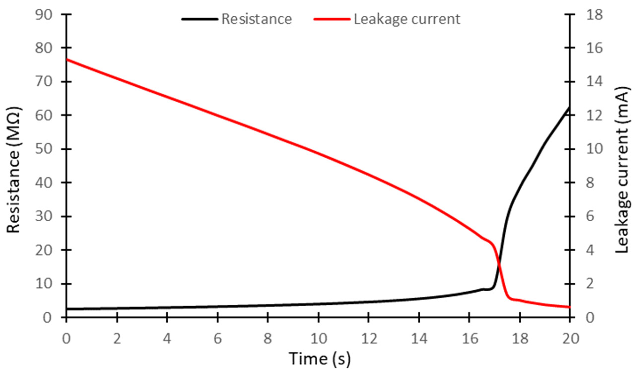
  • The desired voltage was applied to the polluted model, and the leakage current was recorded, to automatically compute the pollution layer resistance until the dry band had completely formed. Simultaneously, the average temperature in the middle of the dry band was also recorded using an IR camera Optris PI400 from Optris Infrared Sensing, Portsmouth, NH, USA.
  • Finally, the ESDD was measured and determined following the procedure described in [19].
To decrease the influence of the experimental parameters, three experimental models of the same substrate material were polluted with the same kaolin and salt solution and tested under the same conditions.

2.2. Surface Conductivity of the Pollution Layer as a Function of the Temperature and ESDD

2.2.1. Procedure and Simplifying Assumptions

The mathematical modeling of the electrical surface conductivity of the pollution layer as a function of the temperature and ESDD was carried out from the results of experimental tests under applied voltages of 2 kVrms and 4 kVrms. Several test series using a Plexiglas substrate material were then conducted for different ESDD levels. For each test, the evolution of the average temperature T and the axial E-field in the middle of the dry band with the pollution layer resistance R were simultaneously recorded [20]. Different tests were conducted for an ESDD level varying from 0.31 mg/cm2 to 1.31 mg/cm2. As described in the following, the test results obtained were processed to extract the evolution of the electrical conductivity of the pollution layer as a function of the average dry band temperature and the ESDD. From the experimental observations, several assumptions were made to establish the pollution layer surface conductivity:
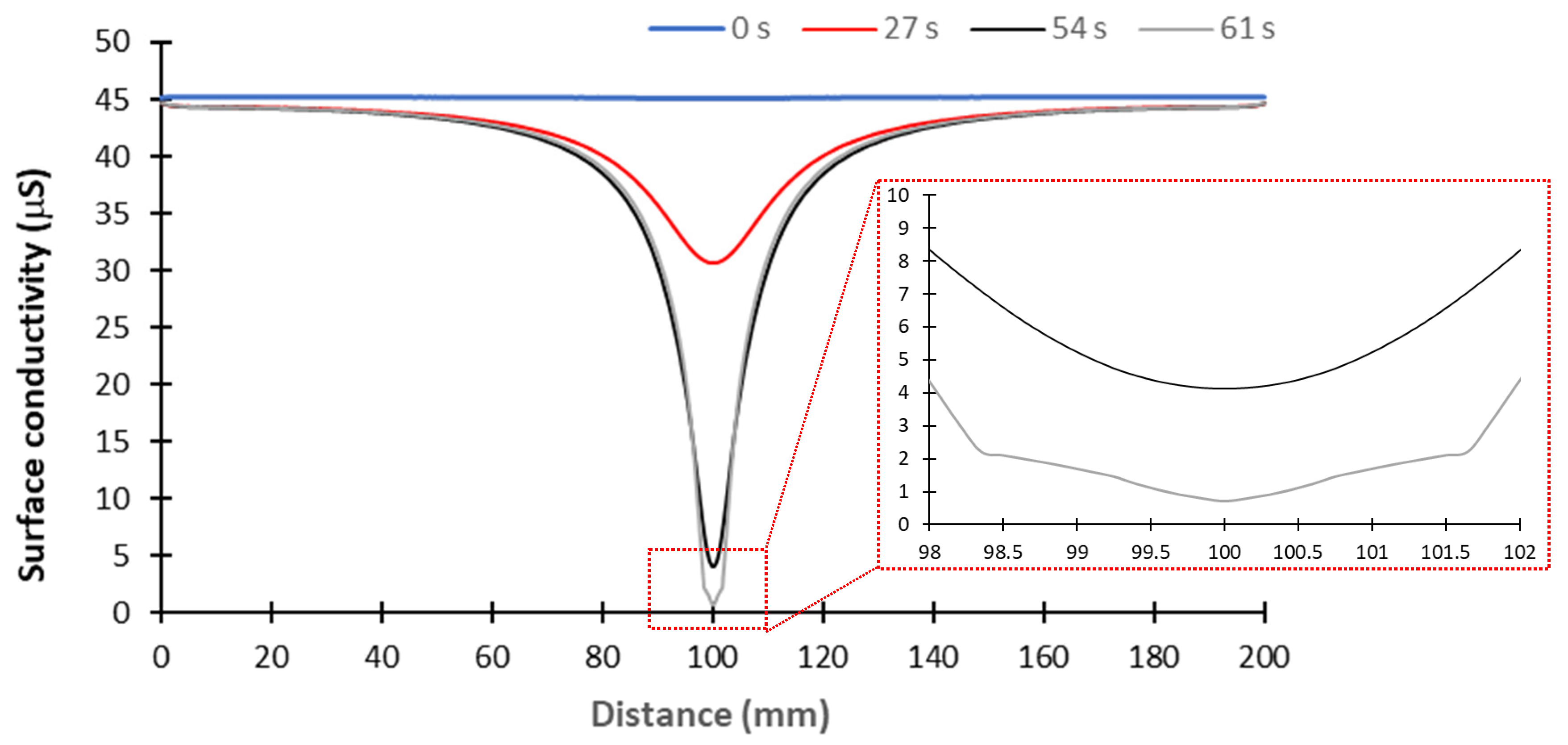
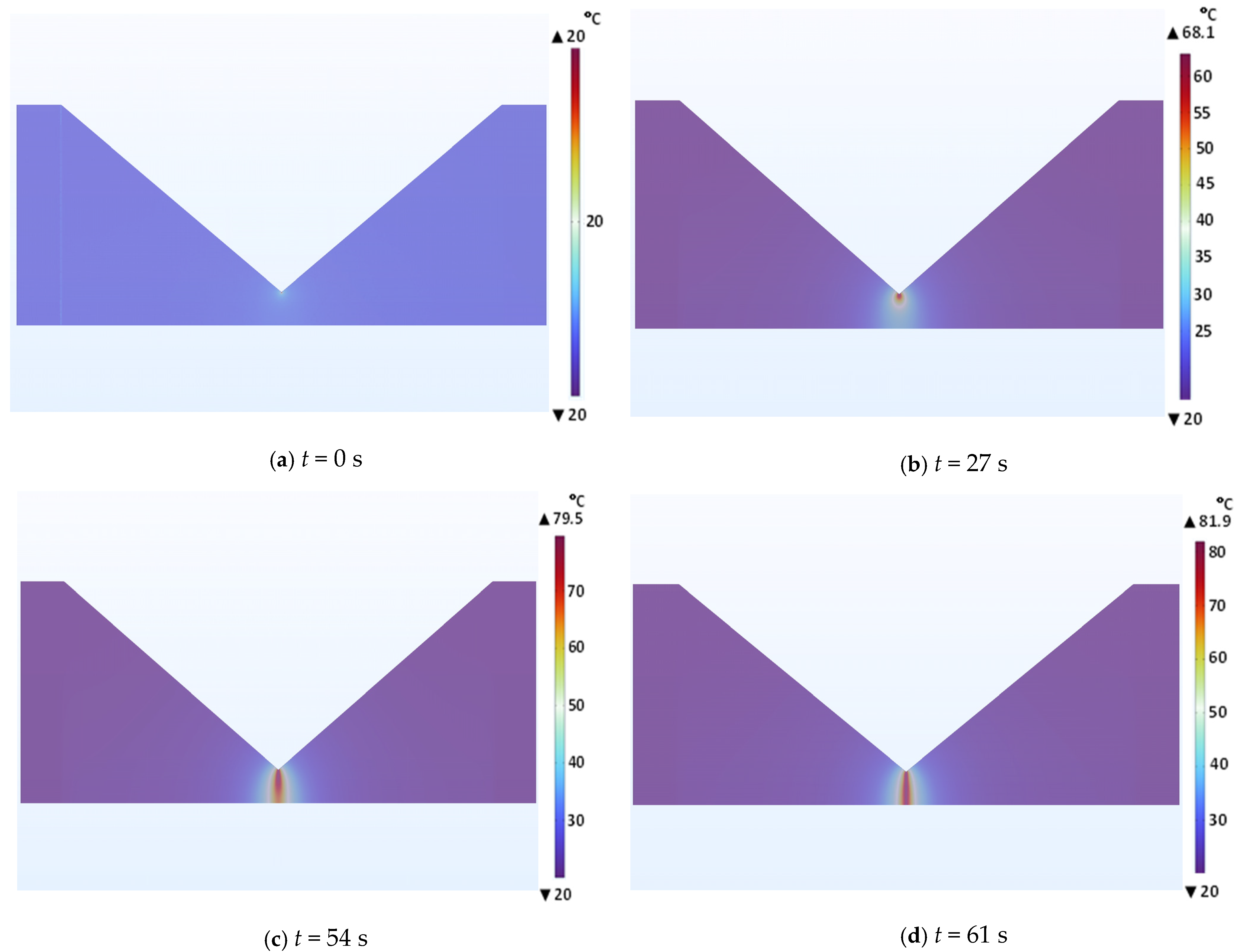
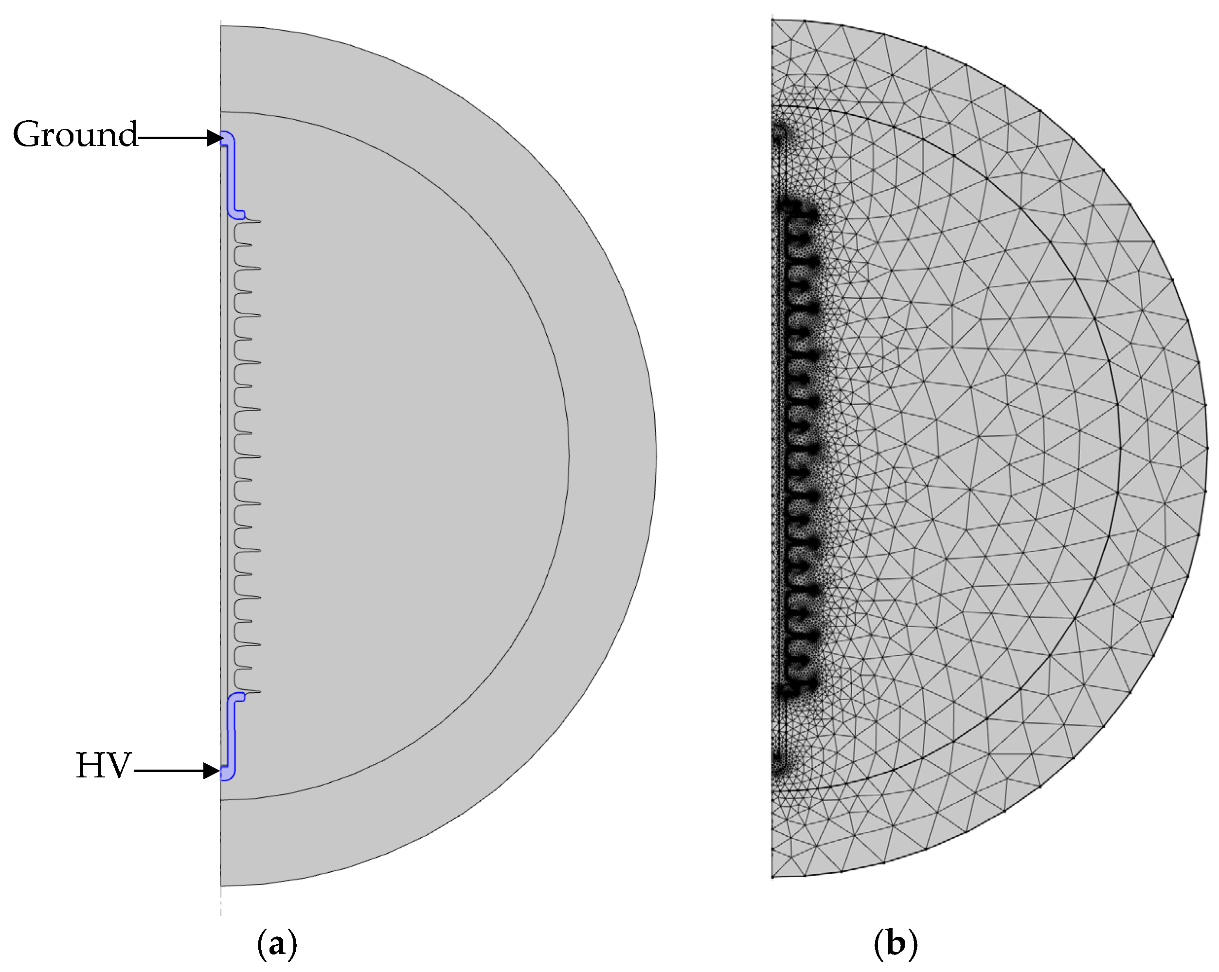
The dry band is uniformly formed in the middle of the flat sample in the stress zone, as illustrated in Figure 1.
The increase in the surface temperature along the flat insulator model occurs principally in the dry band zone, as observed experimentally [19]. This means that the temporal variation in the conductivity (or resistance) of the entire pollution layer is essentially governed by the evolution of the pollution layer conductivity in the dry band zone. In other words, all the electrical parameters such as the pollution layer resistance of leakage current (LC) are governed by the evolution of the dry band resistance.
These hypotheses make it possible to bring the starting geometry back to the zone of appearance of the dry band.

2.2.2. Empirical Pollution Surface Conductivity Equation

The empirical equation of γ s = f ( E S D D ,   T ) was derived using a specific treatment of the data obtained using Matlab R2020a curve fitting tools, as presented in the flowchart in Figure 2. For each test using a Plexiglas substrate and an applied voltage of 4 kV, the evolution of the pollution layer resistance and temperature in the dry band zone were recorded. From these experimental data, the evolution of the surface conductivity γ s and the average temperature in the middle of the dry band were computed, as presented in Figure 2, for an ESDD of 0.83 mg/cm2. Matlab curve fitting tools were then used to determine a mathematical expression for each of the experimental surface conductivity and temperature evolutions (see Figure 2). For the surface conductivity γ s , the general mathematical expression obtained is of the following form:
γ s t = a e b t + c e d t ,
where A, B, k1, and k2 are constant coefficients depending on the ESDD level.
For the temperature T, the general mathematical expression is more complicated and can be expressed as follows:
T = a 1 e t b 1 c 1 2 + a 2 e t b 2 c 2 2 + a 3 e t b 3 c 3 2 + a 4 e t b 4 c 4 2 + a 5 e t b 5 c 5 2 ,
where C, D, E, F, and k3 to k10 are constant coefficients depending on the ESDD level.
By combining Equations (3) and (4), it becomes possible to express the surface conductivity of the pollution layer as a function of its temperature T, eliminating the time dependence. Using Matlab curve fitting tools, the new expression of γ s obtained shows a linear relation with the temperature T, which can be expressed as follows:
γ s T = α T + β ,
where α and β are two constant coefficients depending on the ESDD level. For an ESDD of 0.31 mg/cm2, α = −0.053 and β = 17.27, and for an ESDD of 1.31 mg/cm2, α = −0.044 and β = 15.48.
Finally, putting together all the empirical formulations of Equation (5) obtained for all the ESDD levels, the expression of the pollution layer surface conductivity γ s as a function of the surface temperature T and ESDD level can be obtained. Hence, the surface conductivity γ s ( S ) can then be expressed as a function of the surface temperature T (°K) and ESDD level (mg/cm2) as follows:
γ s T , E S D D = 1.857 × 10 7 T + 3.655 × 10 4 × E S D D 2.934 × 10 4 T × E S D D 0.663 × 10 4 .
Equation (6) is valid only for the duration of the dry band formation defined from the end of the humidification where the voltage is applied to the complete formation of the dry band in the narrow part of the model (Figure 1). Hence, for the same ESDD value, when the surface temperature T is equal to the ambient temperature (20 °C or 293.15 °K), the surface conductivity γ s equals the value obtained at the end of the humidification period. As the surface temperature T increases to 340 °K (or 66.85 °C), the γ s ( T ,   E S D D ) value decreases linearly until it reaches a value close to zero.

3. Thermoelectric Numerical Model of Dry Band Formation

3.1. Presentation of the Model

The numerical model used for all the simulations, presented in Figure 3, considers the simplified insulator model and the climatic chamber. Due to symmetry considerations and to decrease the computation time, only half of the experimental setup was modeled. All the simulations were performed using Comsol Multiphysics©, as it permits the easy coupling of electrical and thermal simulations. Moreover, this commercial software offers the possibility of using specific electrical and thermal boundary conditions to model a thin layer (the pollution layer) [21]. If both the current density and the temperature along the thin layer thickness can be considered as constant, the latter can then be modeled using a specific thermoelectrical boundary condition, where the layer thickness does not need to be discretized using a very small number of finite elements [13,26]. This modeling strategy permits significantly decreasing the number of finite elements required to model the thin layer, as the surface of the insulator envelope is treated as a specific thin electrothermal boundary condition. This is useful when the dimensional ratio is important in the numerical model, for example, in comparing the thickness of the pollution layer (fixed at 0.5 mm) to the length of the climatic chamber (1.2 m). In addition, using the surface approach for the polluted layer facilitates the implementation of the empirical formulation of the pollution surface conductivity given by Equation (6), as this can be directly used in the FEM software material interface. The different thermoelectrical parameters used for the simulation are presented in Table 1.
The different thermoelectric simulations have to be performed using a temporal study in order to simulate the formation of the dry band and then estimate its appearance time. After a preliminary convergence study, the mesh size was fixed with an increase in its density in the dry band zone appearance (see Figure 4). In addition, the convergence study also permitted fixing the time step used for the temporal studies at 1 s.

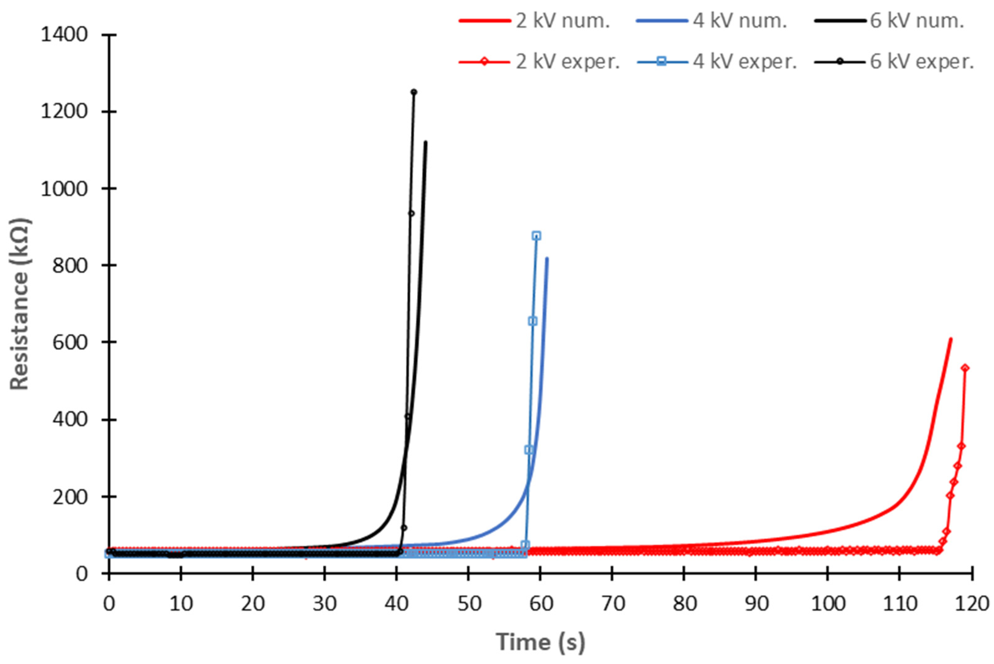
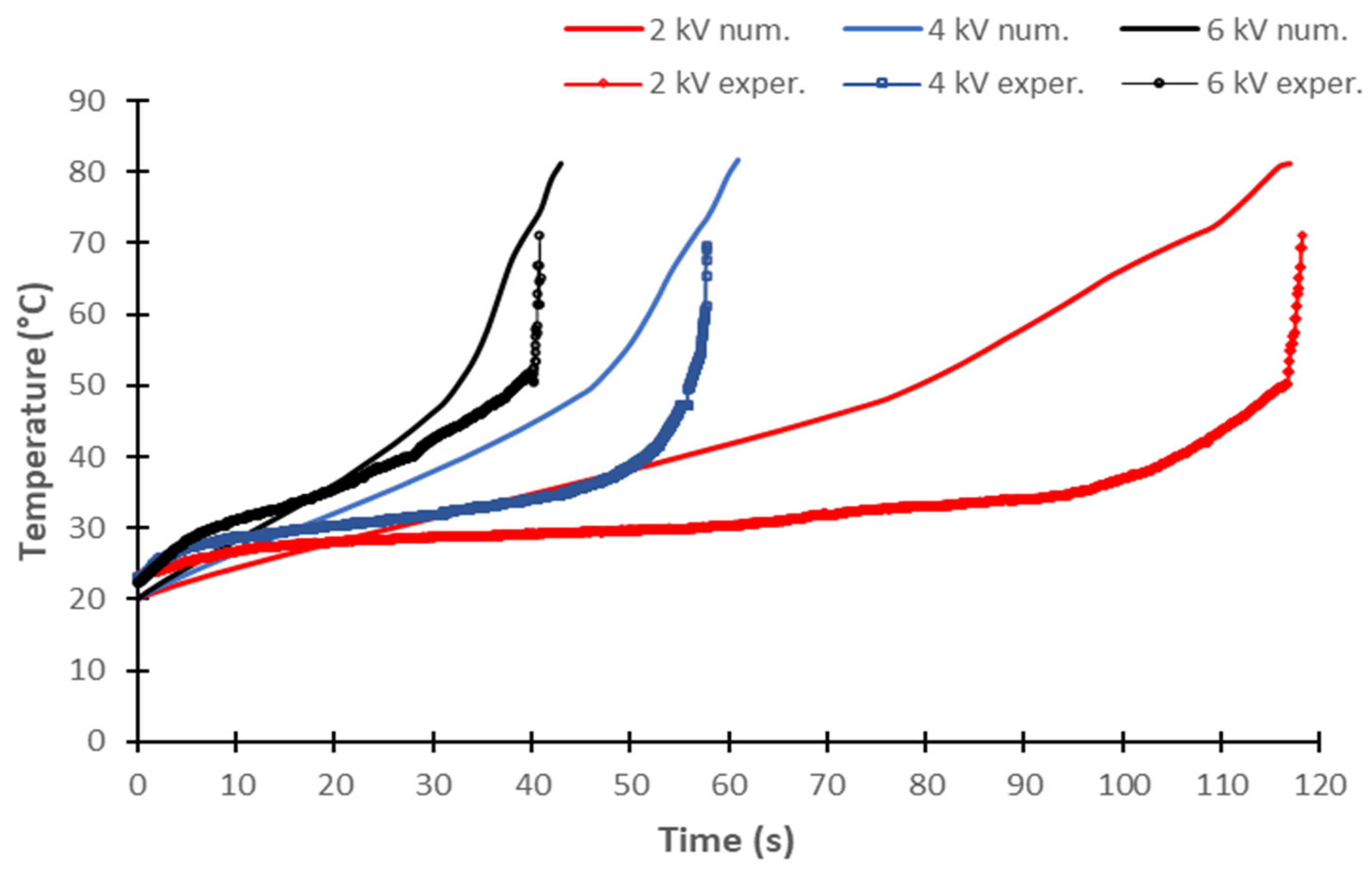
3.2. Validation of the Thermoelectrical Dry Band Formation Simple Model

The first simulations were performed to verify the validity of the empirical surface conductivity formulation given by Equation (6), as well as its implementation in the numerical model using a surface approach for the pollution layer. For this, the experimental results obtained in the previous research with a Plexiglas substrate, an ESDD of 0.31 mg/cm2, and applied voltages of 2 kV, 4 kV, and 6 kV were used for comparison [20]. For all the tests, the ambient temperature of the climatic chamber was fixed at 20 °C. Figure 5 and Figure 6 present the comparison between the experimental and numerical results obtained for the pollution layer resistance and temperature in the middle of the dry band, respectively.
As shown in Figure 5, a relatively good concordance was obtained between the experimental resistance measurements and the resistance in the numerical semi-empirical model. As observed, the pollution layer resistance evolution experimentally and numerically followed the same pattern, which was observable in our previous studies independent of the ESDD value and material substrate [19,20]. This pattern is principally characterized by a very slow linear increase in the resistance layer followed by a sudden jump in it that corresponds to the appearance of the dry band [19,20]. For comparison purposes, the average pollution layer resistance Rav obtained during this slow linear increase was computed, along with the dry band appearance time TDB corresponding to the sudden increase in the resistance value. Hence, the comparison of Rav permits the validation of the electrical part of the thermoelectric simulation while the comparison of TDB permits the validation of the thermal one. The value of TDB for the numerical results was determined using the criterion of a minimum 10% increase in the pollution layer resistance at the next time step. The value of TDB obtained was also used to compute the numerical Rav value. The results obtained numerically were then compared to the experimental ones, as presented in Table 2.
As shown in Table 2, a relatively good concordance was obtained between both the experimental and numerical pollution resistance layer evolution. Indeed, regarding the Rav values, a maximum discrepancy of 18.1% was obtained for 6 kVrms. For the dry band appearance time, TDB, a maximum discrepancy of 7.5% was obtained for an applied voltage of 6 kVrms.
For the evolution of the temperature obtained in the middle of the dry band zone (Figure 6), some differences between the experimental and simulation results can be observed. In particular, the numerical temperature seems to increase more rapidly than the experimental one. This can be explained by the fact that the rate of heat exchange at the surface of the pollution layer in the numerical thermal model was simplified relative to the experimental model. In particular, a small air velocity of around 2.3 m/s at the surface of the polluted model was measured in the climate room during the different tests, which was ignored in the simulation for simplification purposes. To compare the results, the average temperature Tav obtained for the time interval TDB given in Table 2 was computed, along with the maximum temperature Tmax. The results presented in Table 3 show that the discrepancies obtained are of the same order as those obtained for the pollution layer resistance. Hence, these results demonstrate that the surface approach used for the thermoelectrical simulation is valid, as is the implementation of the semi-empirical expression of the surface conductivity proposed in this work.
The numerical model also permits computing the evolutions and distributions of other electrical quantities such as the axial E-field and electrical potential, as well as the surface conductivity γ s ( T ,   E S D D ) given by Equation (6). Figure 7 presents an example of the distribution of the electrical potential at the surface of the pollution layer along the axis of symmetry of the experimental model obtained at 4 kVrms for the following times: 0 s, 27 s, 54 s, and 61 s. Figure 8 presents the distribution of the surface conductivity γ s ( T ,   E S D D ) along the same potential reference line, and Figure 9 presents the corresponding temperature distribution at the surface of the experimental model for the same time step.
The results shown in Figure 7, Figure 8 and Figure 9 clearly illustrate the principle of dry band formation and the evolution of the relative electrical quantities. When the voltage is applied to the polluted sample (t = 0 s), the surface temperature and conductivity γ s ( T ,   E S D D ) are both constant and are minimal and maximal, respectively (Figure 8 and Figure 9a). This results in a quasi-linear distribution of the potential along the symmetry axis of the model (Figure 7). As time passes, the temperature in the dry band zone increases to its maximum (81.9 C) from the edge of the narrow part of the sample (Figure 9b) to the middle part of the sample (Figure 9c) to complete the dry band formation (Figure 9d). The local increase in the temperature in the dry band zone leads to a local decrease in the surface conductivity γ s ( T ,   E S D D ) , as illustrated in Figure 8. As the surface conductivity γ s ( T ,   E S D D ) decreases, the voltage drop across the dry band increases, as demonstrated in Figure 7, to finally equal most of the applied voltage of 4 kVrms at t = 61 s. Moreover, the results shown in Figure 7 and Figure 8 permit the determination of the width of the dry band, which is sensibly equal to 3 mm and of the same order as the values obtained experimentally [19].
Finally, the last electrical quantity studied is the evolution of the axial E-field component in the middle of the dry band zone and at 7.5 mm from the surface of the pollution layer. The evolution of this quantity was experimentally measured using a specific electro-optic E-field sensor as presented in our previous paper [20]. Figure 10 presents the comparison of the experimental and numerical evolutions of the axial E-field component corresponding to the results presented in Figure 5 and Figure 6 for an applied voltage of 4 kVrms. As observed, the numerical evolution of the axial E-field is similar to the experimental evolution, with a final value of the same order, around 1.6 kV/cm. However, the main difference is the sudden increase in the axial E-field for the experimental results, where the increase is more progressive for the numerical ones. This also can be observed in the evolution of the pollution layer resistance (Figure 5) and the temperature (Figure 6).

4. Study of Parameters Influencing the Dry Band Formation

The results presented in the previous section validated the numerical model of the dry band formation using an empirical formulation of the temperature and ESDD-dependent surface conductivity of the pollution layer. Then, with this model, it is possible to study the influence of different model parameters that can influence the formation of the dry band and to verify the limitations of the numerical simulations.

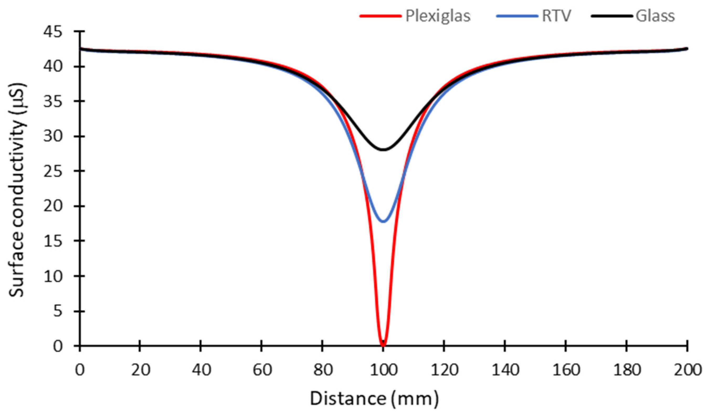
4.1. Influence of the Substrate Thermal Properties

Next, the influence of the thermal properties of the material substrate was investigated. For this, a comparison was performed using three substrate materials: Plexiglas, RTV, and glass, whose thermal properties are presented in Table 1. Figure 11 presents the evolution of the pollution layer resistance and the corresponding temperature evolution in the middle of the dry band. The dry band appearance time TDB is directly affected by the material substrate and, consequently, by its thermal properties, particularly by the thermal conductivity. Indeed, from Table 1, the thermal conductivity of the RTV and glass substrate is around 1.5 and 6.1 times higher than that of Plexiglas, respectively. By comparison, the dry band appearance time TDB for the RTV and glass substrate is around 1.3 and 5.5 times higher than that for Plexiglas, respectively.
From Figure 11, it can be observed that the increase in the temperature in the dry band zone is lower for the glass substrate, compared to RTV and Plexiglas. The temperature increase rate before the appearance of the dry band can be estimated as 0.28 °C/s for the glass substrate, 0.52 °C/s for the RTV, and 0.58 °C/s for the Plexiglas. The higher thermal conductivity of the glass slows the temperature increase in the dry band zone, which in turn reduces the decrease in the surface conductivity of the pollution layer γ s ( T ,   E S D D ) , resulting in a delay in the appearance of the dry band, as demonstrated by the results in Figure 12. This phenomenon was observed during the experimental tests presented in our previous paper with the same substrate materials where the influence of the material thermal conductivity was discussed [20]. From the experimental results obtained, it was found that the TDB for the glass and RTV substrate was around 6 and 3.7 times higher than that for Plexiglas, respectively. The main difference in the numerical TDB for the RTV substrate compared to the experimental value is attributed to its larger surface conductivity obtained for the same ESDD, which is due to its hydrophobicity recovery capability, as explained in [20].

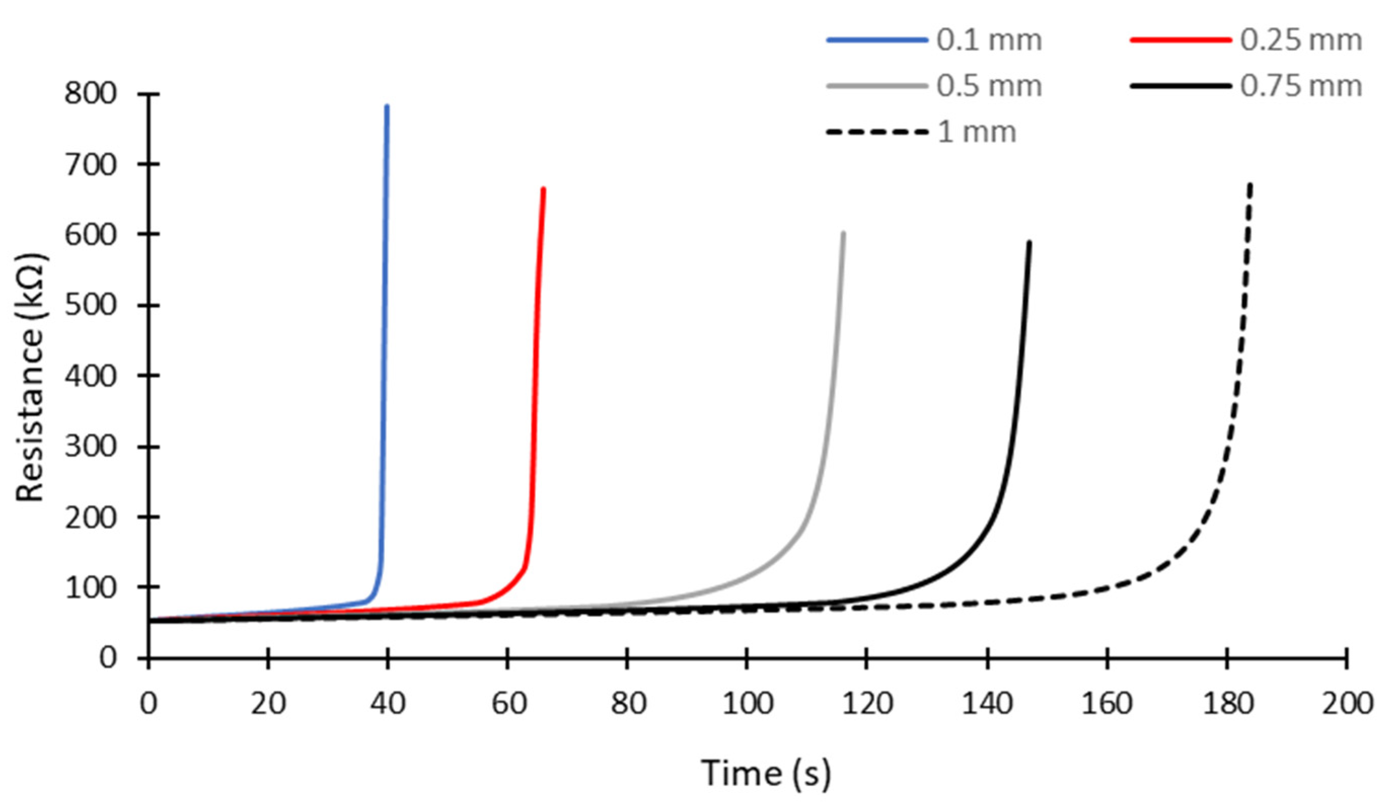
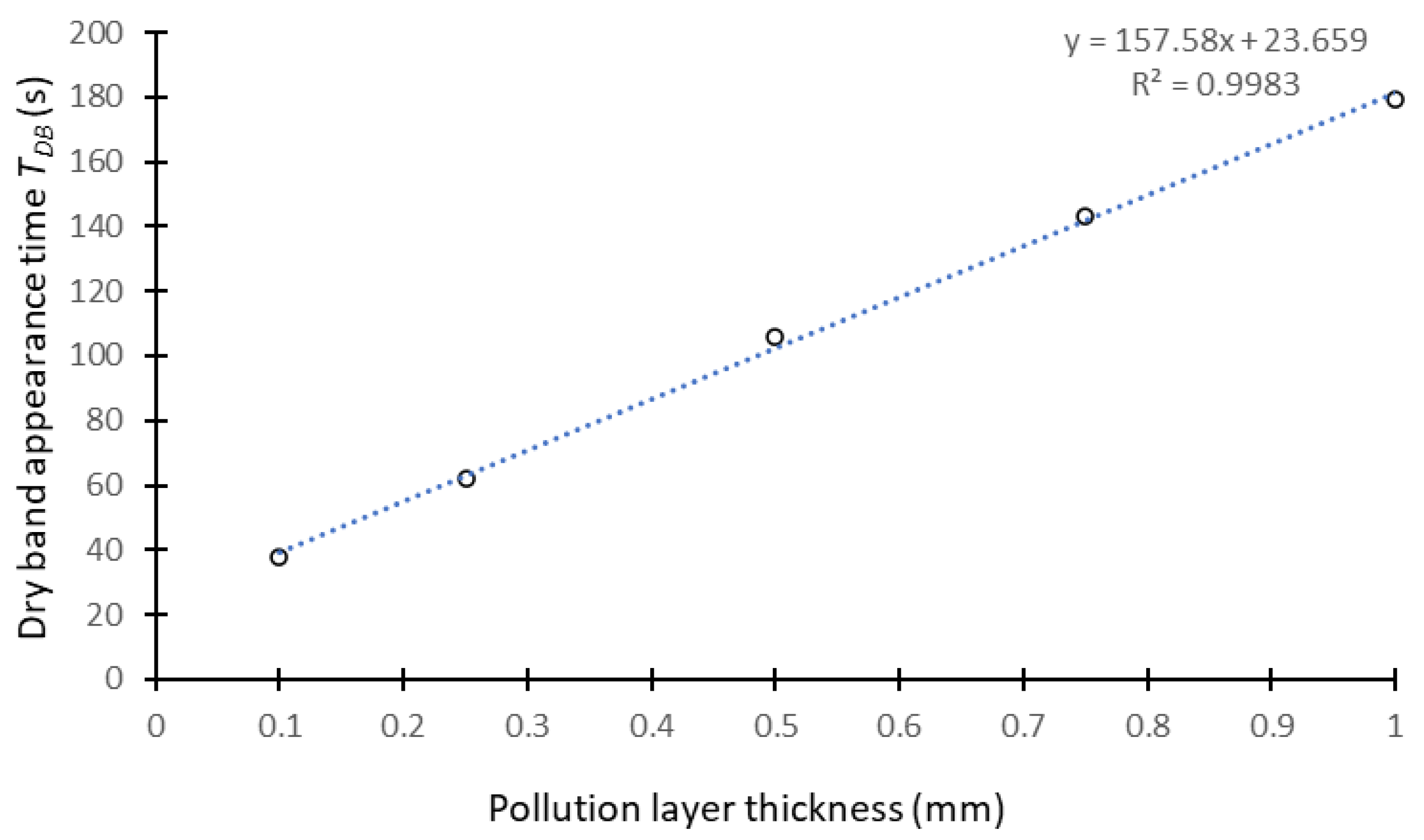
4.2. Influence of the Pollution Layer Thickness

As mentioned previously, the different numerical models of the formation of a dry band on a simple polluted insulator geometry use a surface approach in order to simulate the thermoelectrical behavior of the pollution layer. Even if the thickness of the pollution layer is not physically modeled, the FEM software takes it into account for the thermal part of the modeling. However, for the electrical part, the surface conductivity expression γ s ( T ,   D D S E ) is divided by the thickness of the pollution layer in order to obtain the same volume of electrical conductivity and, consequently, the same resistance for the pollution layer. In this condition, as the applied voltage is the same, the leakage current flowing in the pollution layer is the same, and, consequently, the Joule effect energy, which is also the thermal energy injected in the pollution layer, is the same.
Figure 13 presents the comparison of the pollution layer resistance obtained with different pollution layer thicknesses, for the same ESDD of 0.31 mg/cm2, an applied voltage of 2 kVrms, and a Plexiglas substrate. The results obtained demonstrate the dependency of the dry band appearance time TDB on the thickness of the pollution layer. Moreover, from the results shown in Figure 14, TDB increases linearly with the increase in the pollution layer thickness, for the same pollution layer surface resistance and substrate material. This result demonstrates that the pollution layer thickness can play a significant role in the appearance of the dry band by influencing the temperature distribution inside the pollution layer. The greater the thickness of the layer, the longer it will take for the dry band to appear. However, such results are difficult to verify experimentally as the measurement of the pollution layer thickness remains a complex task depending on the method used to apply the pollution layer, the method employed during the humidification phase, and the material substrate [27].

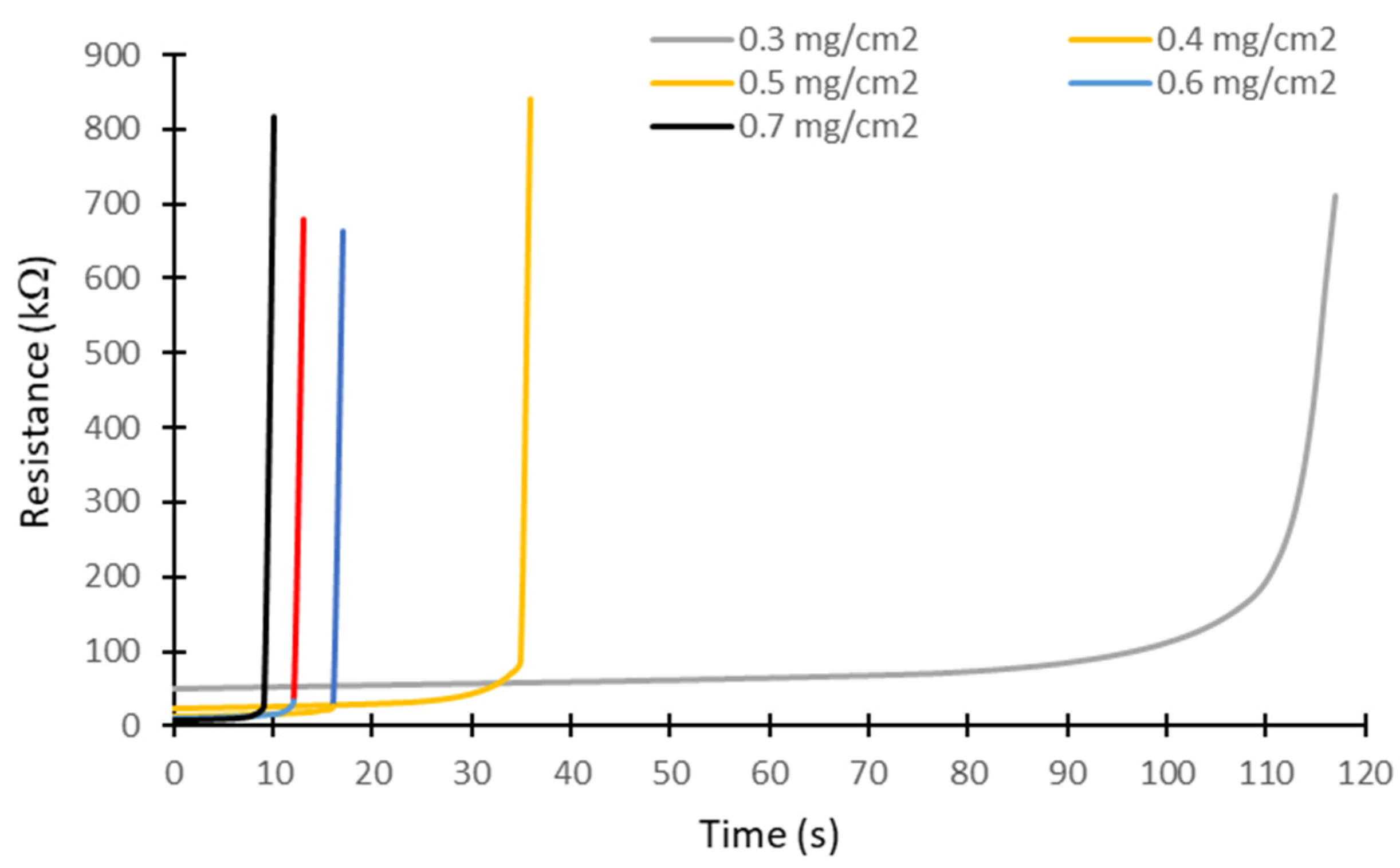
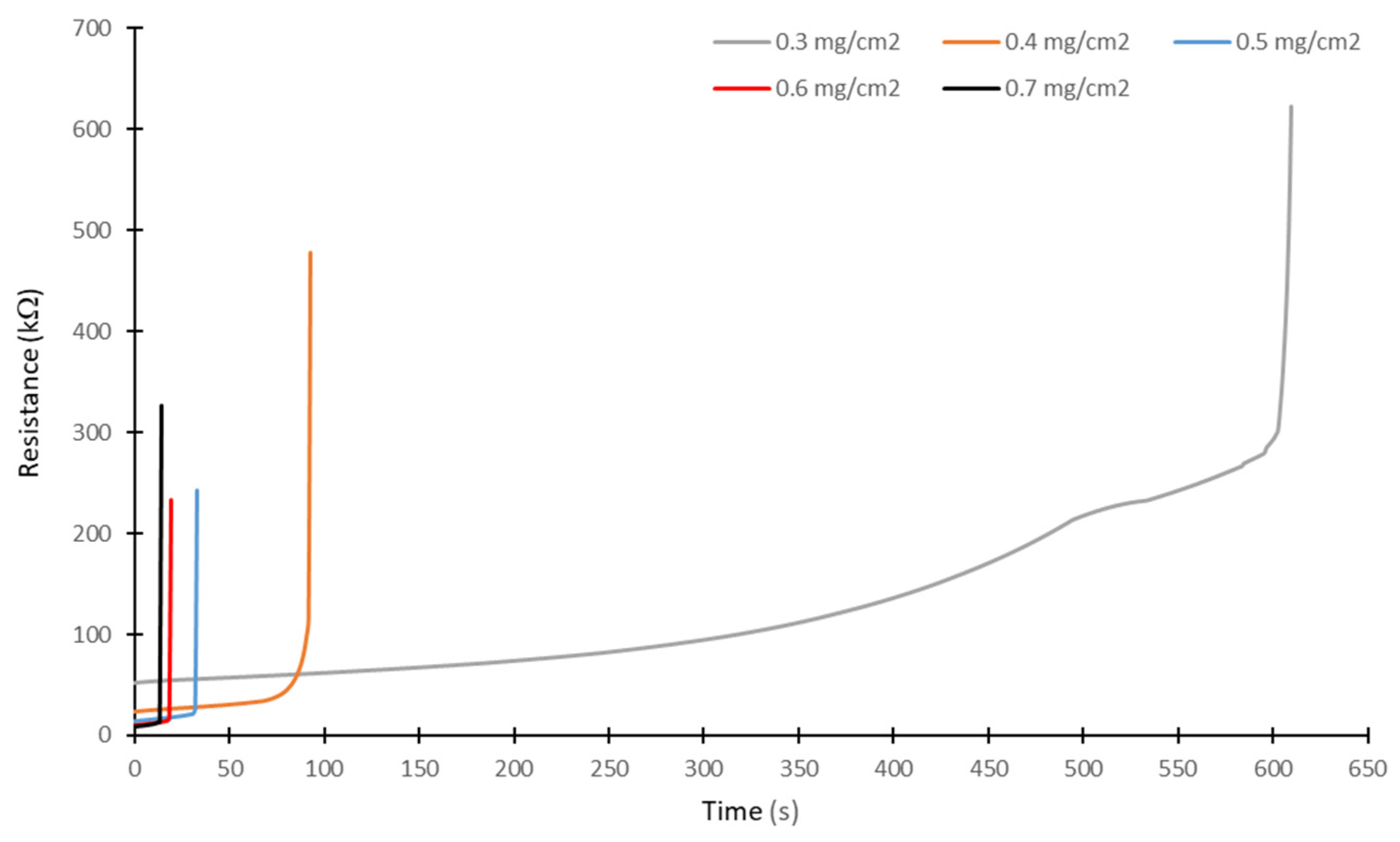
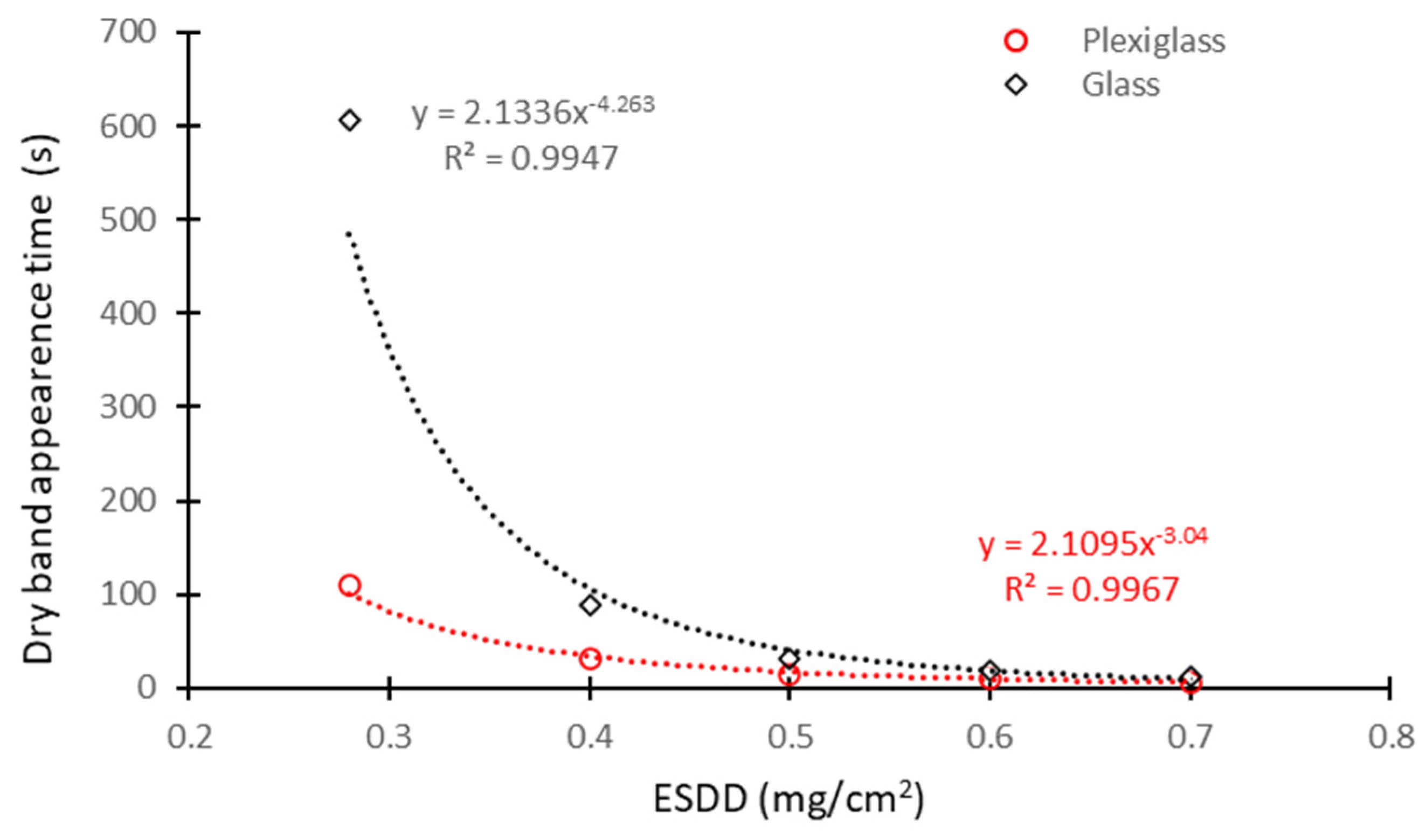
4.3. Influence of the Pollution Layer ESDD

In this subsection, the influence of the ESDD level on the dry band formation on both the Plexiglas and glass substrates is described. Simulations were performed for a pollution layer thickness of 0.5 mm with an applied voltage of 2 kVrms. Figure 15 and Figure 16 present the evolution of the pollution layer resistance as a function of the ESDD level for the Plexiglas and glass substrates, respectively. The appearance of the dry band is delayed as the ESDD level increases, as demonstrated by the results shown in Figure 17. Here, the dry band appearance time (TDB) was computed as a function of the ESDD level for the Plexiglas and glass substrates. It is interesting to note that TDB decreases drastically, as the ESDD level increases, following a regression power curve. This trend can be observed for both substrates.
As expected from Equation (6), the surface conductivity γ s T ,   E S D D increases linearly with the increase in the ESDD level. In that situation, for the same applied voltage, the leakage current flowing in the pollution layer increases, leading to a reduction in the dry band appearance time. From the results shown in Figure 17, the formation of the dry band seems to significantly slow as the ESDD level increases. However, this result does not seem to be representative of the experimental results obtained in our previous study, where the opposite phenomenon was obtained for a glass substrate [20]. Indeed, in our previous study, the dry band appearance time TDB increased with the ESDD level, following a power function [20]. This significant difference in the experimental and numerical results can be attributed to the thickness of the pollution layer used in the simulations, which was kept constant and equal to 0.5 mm. As reported in [28] and also verified in our previous work [19], as the ESDD level increases, the quantity of water absorbed by the pollution layer increases too, leading to an increase in its thickness. This means that as the ESDD level increases, the thickness of the pollution layer should be increased in order to better simulate its influence on the thermal process associated with the dry band formation.

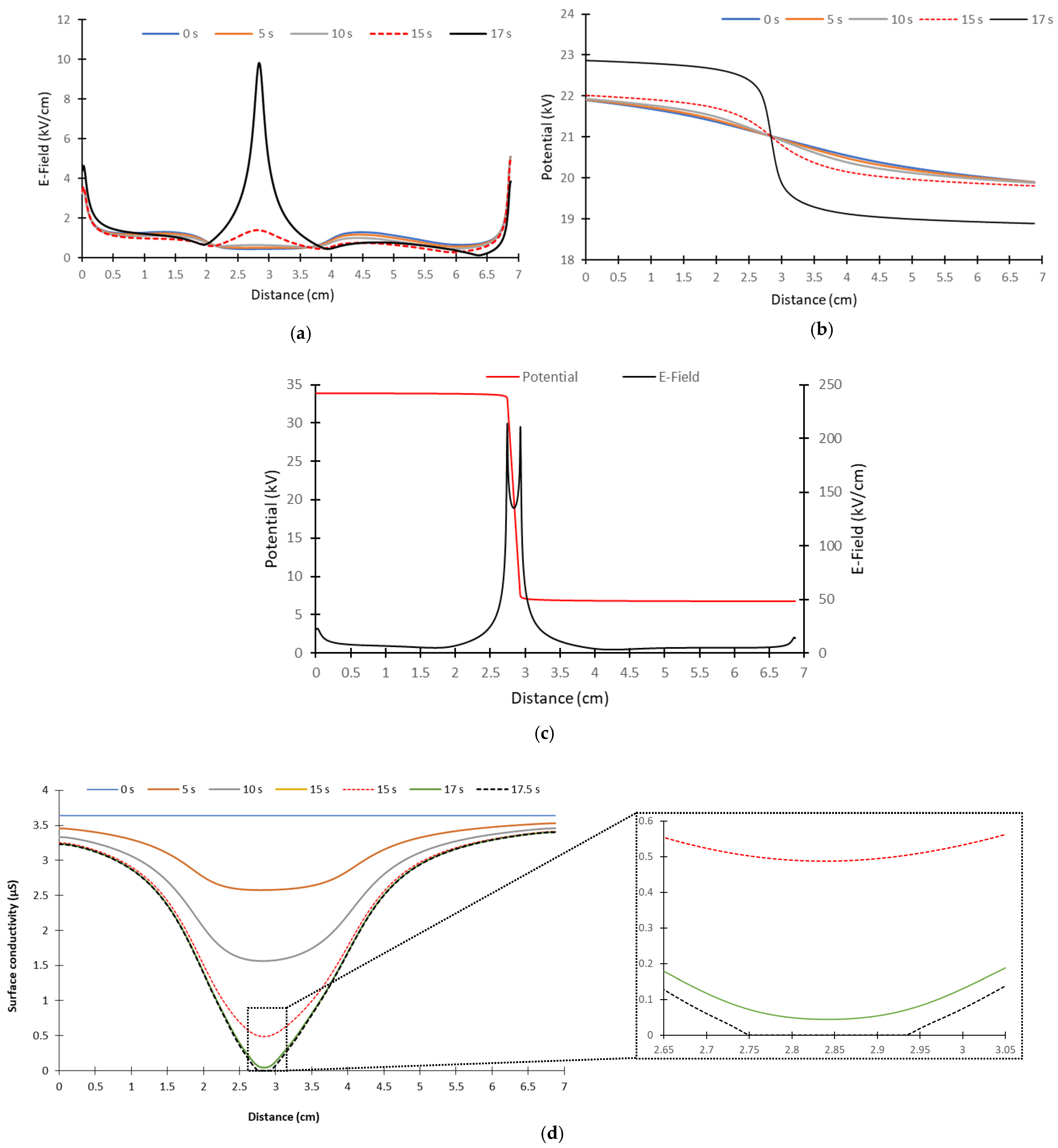
5. Application to a Polluted Composite Insulator

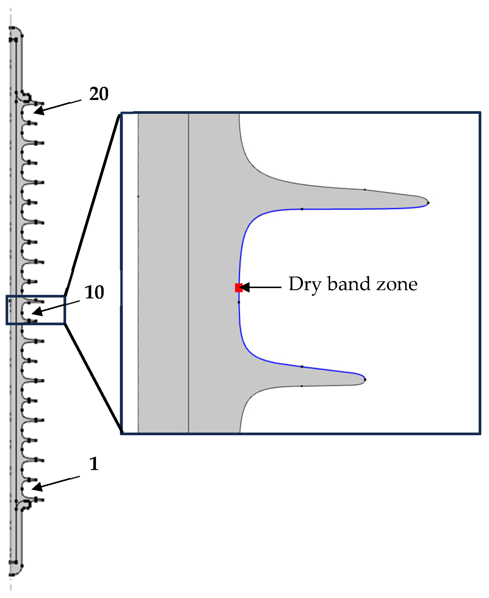
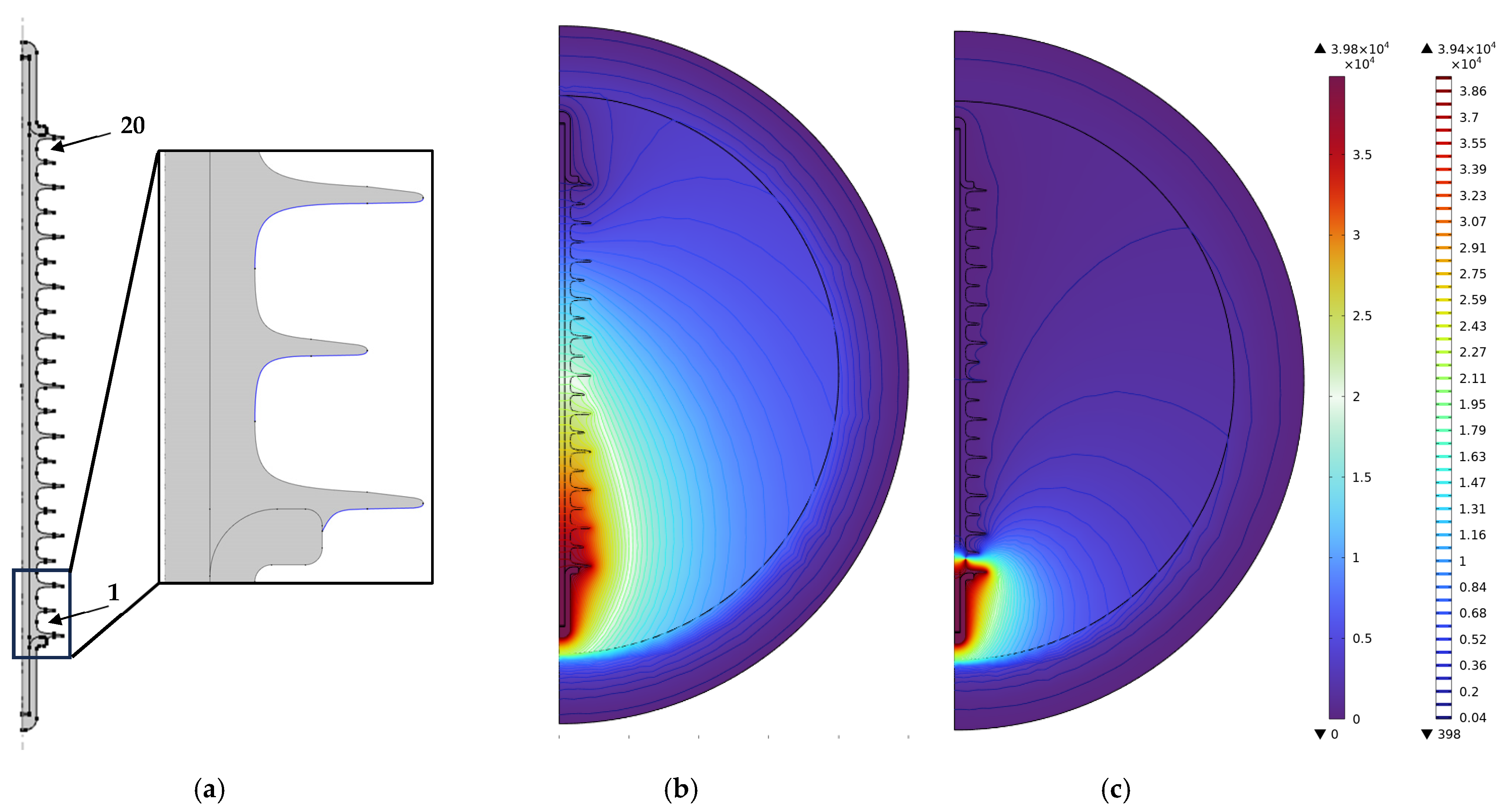
5.1. Polluted Composite Insulator Model

For this part of the study, the empirical formulation of the surface conductivity γ s ( T ,   E S D D ) given by Equation (6) was applied to a uniformly polluted 69 kV Sediver composite insulator. As the pollution layer was considered uniform along the entire surface of the insulator, a 2D axisymmetric finite element method (FEM) using the commercial software Comsol Multiphysics® was then employed. The dimensions of the composite insulator are presented in Table 4. The different simulations were performed using the thermoelectric properties presented in Table 5.
Figure 18 presents the 2D axisymmetric model of the 69 kV Sediver composite insulator, where the pollution layer was considered as a uniform layer with a constant thickness of 0.5 mm. Moreover, the surface approach used previously was employed to model the pollution layer to significantly decrease the computation time, as explained for the simple polluted insulator model. Due to the small number of elements compared to the 3D model used previously (Figure 4), the time step used in the temporal thermoelectrical simulation was fixed at 0.5 s with a phase-to-ground voltage of 39.84 kV applied to the composite insulator.

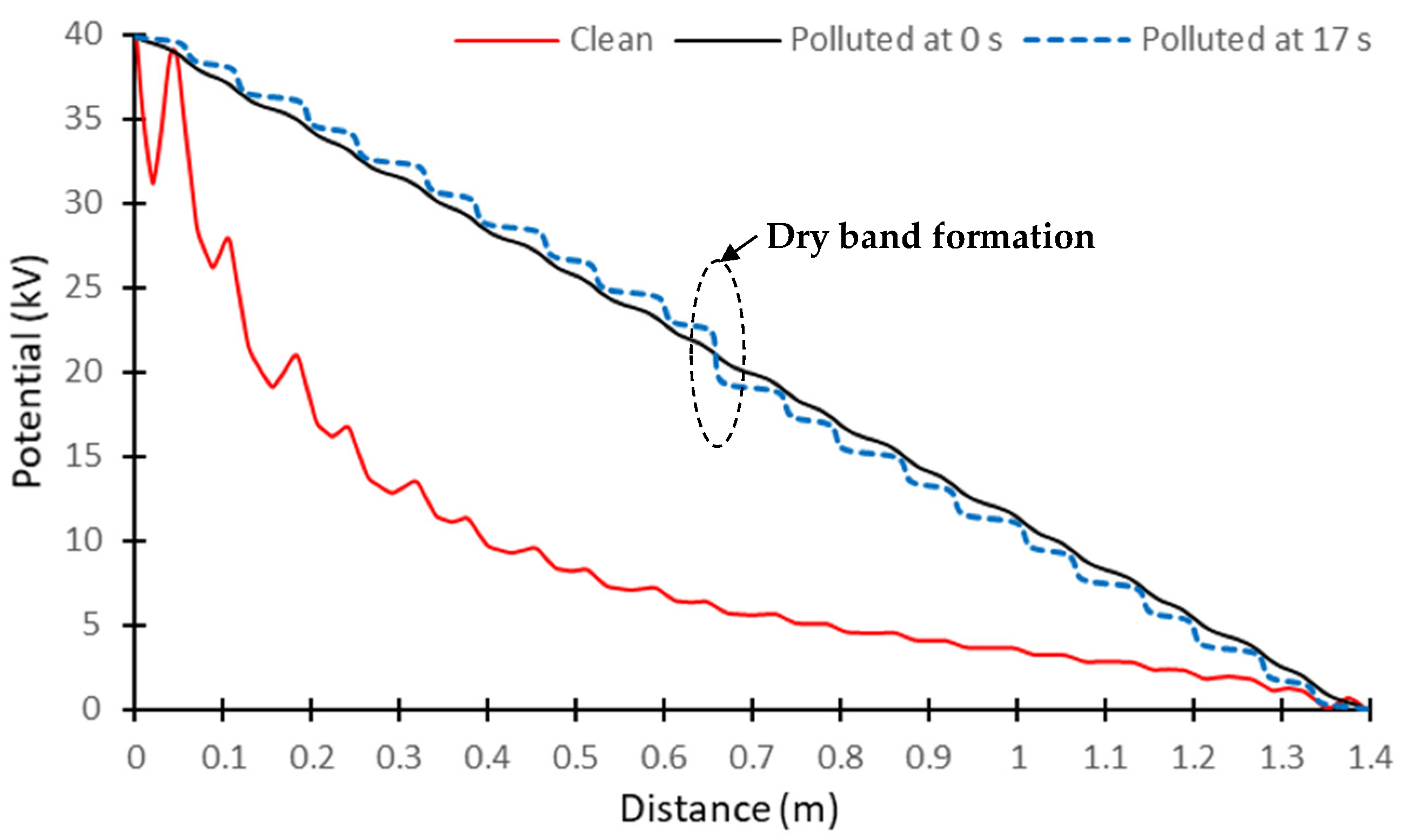
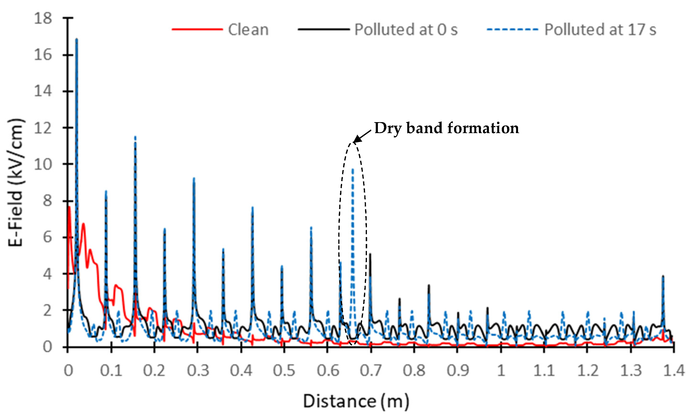
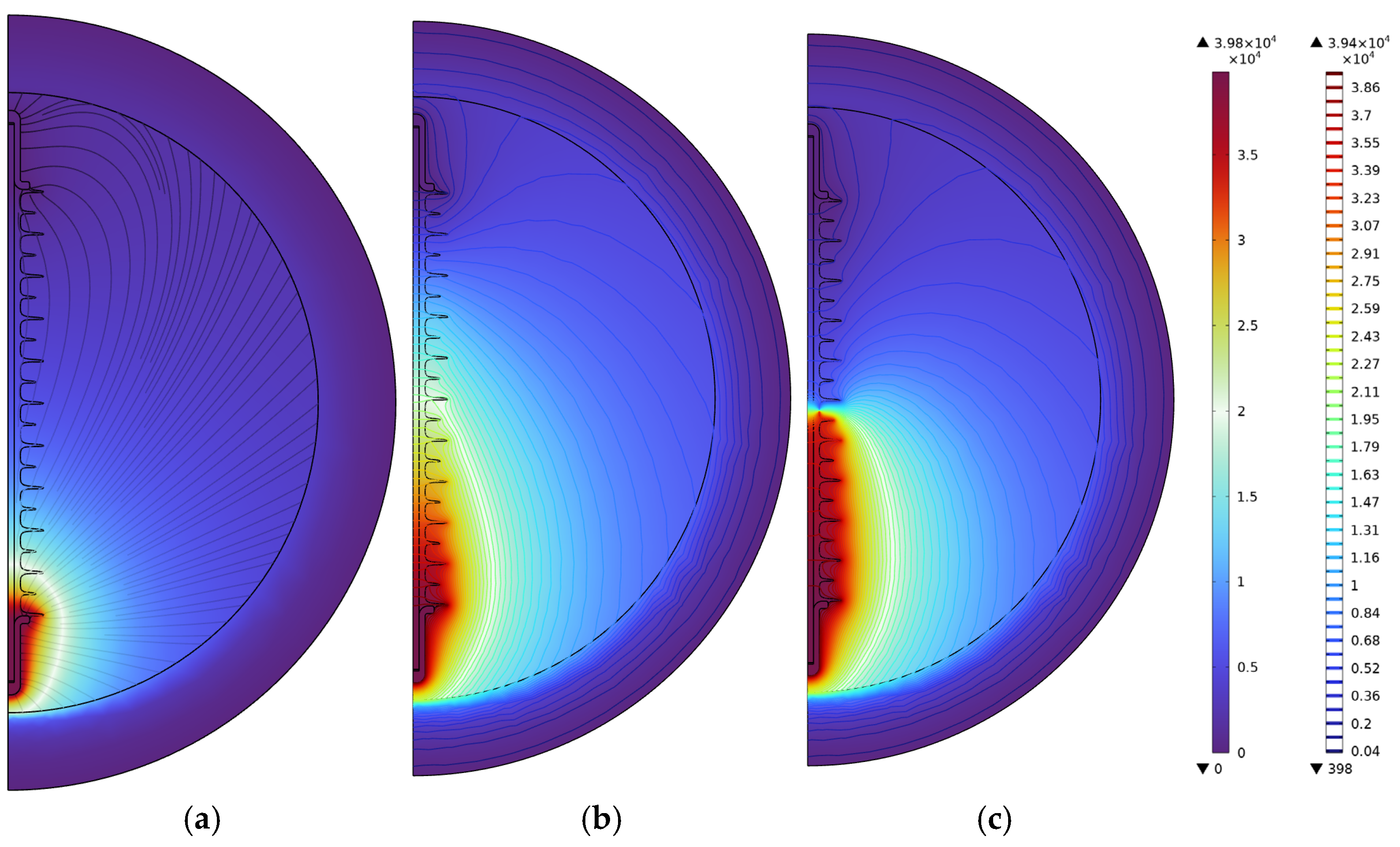
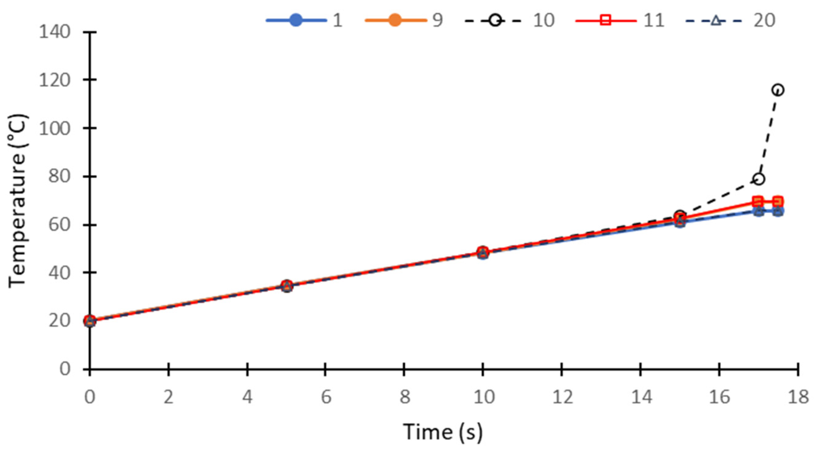
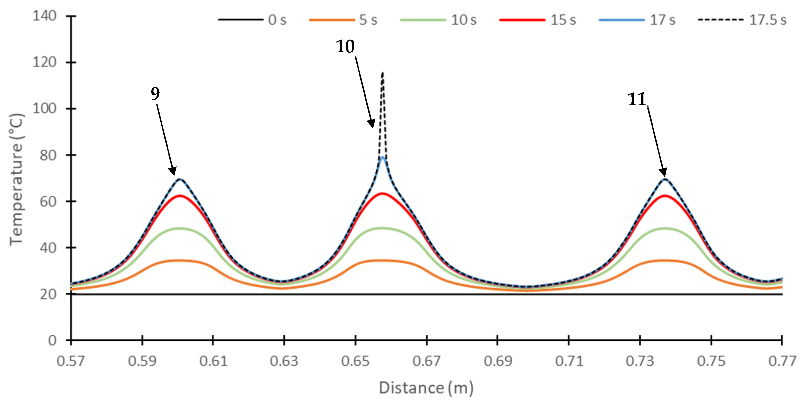
5.2. Numerical Results Relative to the Electrical Parameters

Figure 19 presents the evolution of the leakage current and the pollution layer resistance obtained for an ESDD of 0.31 mg/cm2. The appearance of the dry band leads to a drastic decrease in the leakage current and a sudden increase in the pollution layer resistance, which occur at 17 s. This time step corresponds to the beginning of the dry band formation. The sudden decrease in the leakage current, corresponding to a loss of surface conductivity, is strongly indicative of the formation of local drying, as experimentally observed on composite insulators [6].
Figure 20 and Figure 21 present the comparison of the potential and E-field distributions along the clean insulator compared to the distributions obtained for the polluted insulator at time steps of 0 s and 17 s with an ESDD of 0.31 mg/cm2. The distributions were computed along the leakage distance of the insulator.
Figure 22 presents the distribution of the E-field and potential along the polluted insulator at a time step of 17.5 s when the dry band is formed. Compared to the distributions shown in Figure 20 and Figure 21, the results in Figure 22 clearly demonstrate the presence of the dry band in the middle of the insulator, where most of the voltage applied to the insulator is also applied to the dry band, resulting in a large increase in the E-field strength, which is largely sufficient to induce a partial arc along the dry band.
The position and the influence of the dry band on the potential distribution along the polluted insulator are clearly visible in Figure 23, which shows the surface potential and equipotential line distribution obtained for the clean insulator (Figure 23a), the polluted insulator at t = 0 s (Figure 23b), and the polluted insulator at t = 17.5 s (Figure 23c), where the dry band is present in the middle of the insulator. The influence of the pollution layer on the potential distribution is also clearly illustrated.
To closely see what occurs in the zone of the dry band appearance, the evolution of the potential, E-field, and surface conductivity distribution was computed along the reference line in blue in Figure 24. The results obtained for the different distributions for time steps of 0, 5, 10, 15, 17, and 17.5 are presented in Figure 25.
A closer view of the different distributions presented in Figure 25 clearly shows the evolution of the E-field (Figure 25a) and potential (Figure 25b) distributions before the appearance of the dry band. As the surface conductivity γ s ( T ,   E S D D ) decreases locally in the dry band zone (Figure 25d), the voltage drop along the dry band zone increases, as does the E-field strength (Figure 25a,b). At t = 17.5 s, the dry band is completely formed, as observed in the closer view of Figure 25d, where the surface conductivity value is close to zero at a distance of around 2 mm, which represents the width of the dry band. This leads to a sudden increase in the voltage drop, as well as a significant increase in the E-field strength along the dry band, as demonstrated by the results in Figure 25c.

5.3. Numerical Results Relative to Thermal Parameters

Figure 26 presents the evolution of the surface temperature distribution along the insulator leakage distance. As expected, the maximum surface temperatures are obtained between the sheds at the surface of the insulator rod, whose positions are numbered in Figure 24: position 1 is close to the HV, and position 20 is close to the ground. As the time increases, the maximum temperature at each position between sheds increases in the same manner until 15 s. After that time, the equality between the maximum temperatures is lost at position 10 (middle of insulator), where the maximum temperature seems to increase more rapidly than the other positions (9 and 11, for example at 69.6 °C) until 116 °C, except positions 1 and 10 (insulator extremities), where a decrease in the maximum temperature is observed compared to other positions (9 and 11, for example). The maximum temperature at positions 2 to 9 and 11 to 19 remains the same during the formation of the dry band.
To illustrate this phenomenon, the evolution of the maximum temperature at positions 1, 9, 10, 11, and 20 for the time step in Figure 26 is computed and presented in Figure 27. The maximum temperatures remain the same until 15 s, where the maximum temperature at position 10 increases rapidly to 116 °C at 17.5 s when the dry band is completely formed. This can be compared to the 69.6 °C obtained at positions 9 and 11 and to the 65.9 °C at positions 1 and 20. Except at position 10 where the dry band is formed, the maximum temperature at the other positions does not increase between 17 s and 17.5 s (Figure 27).
Figure 28 presents the evolution of the temperature distribution at the surface of the polluted insulator corresponding to the time steps used in Figure 26. As observed previously, the maximum temperatures occur at the insulator rod surface between the sheds. The maximum temperatures evolve in the same manner (Figure 28a–c) and start to change until the complete formation of the dry band, whose position is clearly observable in Figure 28f.
Finally, Figure 29 presents a closer view of the surface temperature along a portion of the leakage distance between positions 9 and 11 to show the temperature evolution in the dry band zone in detail. The difference in the formation of the dry band due to the local temperature increase is noticeable only in the last 2.5 s, where a sudden increase in the temperature distribution is obtained compared to positions 9 and 11. The sudden change in the local temperature explained the formation of the dry band at this particular position.

5.4. Discussion of the Results Obtained

The different results presented in this section seem to demonstrate that under the specific condition of a uniformly polluted insulator, the dry band seems to appear at the insulator rod surface between the sheds, which is consistent with the experimental observations of real composite insulators [6,12,29]. However, the results also reveal that the first dry band seems to form in the middle of the insulator (position 10 in Figure 24), as illustrated by the results shown in Figure 23 and Figure 28. This result is also consistent with the experimental observation reported in [6,29]. The results also demonstrate that under a uniform pollution layer, the distribution of the surface temperature at the rod surface is sensibly the same along the insulator but starts to differ only in the few last seconds before the dry band formation, as illustrated by the results shown in Figure 26, Figure 27, Figure 28 and Figure 29. This means that a small local change in the surface temperature, as observed in Figure 29, can suddenly lead to the formation of a dry band along the polluted insulator, as reported in [29].
Such a situation can be found with a non-uniform pollution distribution along the insulator, which can be obtained either by a different surface conductivity distribution or by a different pollution layer thickness [30,31,32]. From the different on-site observations, the contamination of the insulator bottom shed surface appears more serious than that on the top by a factor of up to 20, especially for the sheds close to the HV insulator end [32]. To illustrate this, a simulation with a non-uniform pollution distribution was performed by simply modifying the thickness of the pollution layer (1 mm instead of 0.5 mm) on the bottom of the first three sheds, as illustrated by the blue lines of the closer view in Figure 30a. As shown in Figure 30c, the dry band appears after 5.5 s, but now, it is formed at position 1 close to the HV electrode. This result demonstrates that the non-uniformity of the pollution layer directly influences the position of the dry bands, and this non-uniformity can easily be taken into account with the numerical method proposed in this work.
The simulation results have also permitted a detailed study of the evolution of the potential and E-field distribution in the dry band formation zone. As illustrated in Figure 25c, the E-field distribution obtained along the dry band of 2 mm width presents a typical U-shape distribution, which was obtained in different simulations of polluted insulators [10,11,12].

6. Conclusions

The use of a simple flat geometry permitted an experimental simulation of the complex phenomenon of the formation of a dry band on polluted insulators. By precisely controlling the zone of the dry band appearance and recording the evolution of the surface temperature and pollution layer resistance, it was possible to define a simple expression of the surface conductivity of a pollution layer as a function of the average surface temperature inside the dry band and the ESDD. Hence, for a fixed ESDD value, the surface conductivity γ s ( T ,   E S D D ) decreases linearly with the increase in the surface temperature.
Due to its simplicity, the surface conductivity expression was easily implemented in the commercial FEM software Comsol Multiphysics, which enables modeling the pollution layer using a specific thermoelectrical boundary condition. This combination led us to propose, to the best of our knowledge, the first simple thermoelectric surface model of a pollution layer, which can simulate the temporal evolution of the pollution layer resistance until the formation of the dry band, considering the electrothermal properties of the insulator material. The proposed pollution layer model was validated with experimental results on a Plexiglas substrate, where a maximum discrepancy of 18.1% was obtained for the average pollution layer resistance and 17.8% for the maximum temperature. For the temporal part of the simulations, a maximum discrepancy of 7.5% was obtained in the dry band appearance time.
The results also demonstrated that the thermoelectric surface model can consider the influence of the thermal properties of the substrate materials on which the pollution layer is deposited. This represents a significant advantage over models based solely on E-field considerations to express the thermal power dissipated in the pollution layer.
The different simulations also permitted highlighting the thermal influence of the pollution layer thickness on the time to dry band formation as well as the influence of the ESDD level. In particular, the proposed model was not able to reproduce the experimental results where the dry band appearance time increased with the ESDD level increase. This significant difference can be explained by the fact that as the ESDD level increased, the pollution layer increased, which can result in an increase in the dry band appearance time. It might then be interesting to define a relationship between the ESDD level and the pollution layer thickness, which could then be easily implemented in the numerical model.
Moreover, the proposed thermoelectric surface model was used to axisymmetrically simulate in 2D a uniformly polluted 69 kV composite insulator. As demonstrated, under uniform pollution, the dry band appears in the middle of the insulator length. The model also permits following the temporal evolution of the surface temperature, the potential, and the E-field distributions, which are of great interest for the comprehension of the insulator behavior under polluted conditions. It was also demonstrated by a simple simulation that the thermoelectrical surface model can easily consider a non-uniform pollution layer with a dry band formed between the first two sheds close to the HV electrode.
In conclusion, the thermoelectric surface model can provide an interesting tool for numerically studying the influence of different parameters relative to the pollution layer and the insulator material and geometry. Hence, the proposed model can help to study and develop new types of mitigation methods to improve the performance of all types of insulators under polluted conditions. In addition, these new mitigation methods could then be easily tested with the simple flat insulator geometry used in our previous studies, which can experimentally reproduce the formation of a dry band.

Author Contributions

Numerical simulations were performed by M.-A.A. and G.K. M.-A.A. was also responsible for the experimental investigation and the original draft preparation. Validation, review and editing, visualization, and supervision were the responsibility of C.V., who was also responsible for funding acquisition. All authors have read and agreed to the published version of the manuscript.

Funding

The authors thank the Natural Sciences and Engineering Research Council of Canada for financial support (Discovery grant RGPIN-2019-06700).

Data Availability Statement

The original contributions presented in this study are included in the article. Further inquiries can be directed to the corresponding author.

Conflicts of Interest

The authors declare no conflicts of interest.

References

  1. Williams, D.L.; Haddad, A.; Rowlands, A.R.; Young, H.M.; Waters, R.T. Formation and characterization of dry bands in clean fog on polluted insulators. IEEE Trans. Dielectr. Electr. Insul. 1999, 6, 724–731. [Google Scholar] [CrossRef]
  2. Albano, M.; Haddad, A.M.; Bungay, N. Is the dry-band characteristic a function of pollution and insulator design? Energies 2019, 12, 3607. [Google Scholar] [CrossRef]
  3. Bo, L.; Gorur, R.S. Modeling flashover of AC outdoor insulators under contaminated conditions with dry band formation and arcing. IEEE Trans. Dielectr. Electr. Insul. 2012, 19, 1037–1043. [Google Scholar] [CrossRef]
  4. Gençoğlu, M.T.; Cebeci, M. The pollution flashover on high voltage insulators. Electr. Power Syst. Res. 2008, 78, 1914–1921. [Google Scholar] [CrossRef]
  5. Zhang, D.; Meng, F. Research on the interrelation between temperature distribution and dry band on wet contaminated insulators. Energies 2019, 12, 4289. [Google Scholar] [CrossRef]
  6. Albano, M.; Waters, R.T.; Charalampidis, P.; Griffiths, H.; Haddad, A. Infrared analysis of dry-band flashover of silicone rubber insulators. IEEE Trans. Dielectr. Electr. Insul. 2016, 23, 304–310. [Google Scholar] [CrossRef]
  7. Loberg, J.O.; Salthouse, E.C. Dry-Band Growth on Polluted Insulation. IEEE Trans. Electr. Insul. 1971, 6, 136–141. [Google Scholar] [CrossRef]
  8. Yang, H.; Cao, W.; Wen, R.; Wang, Y.; Shen, W.; Zhang, L. Study on surface conductivity distribution of pollution layer during the propagation of local arc on the wet polluted insulation surface. AIP Adv. 2022, 12, 015311. [Google Scholar] [CrossRef]
  9. He, J.; He, K.; Gao, B. Modeling of Dry Band Formation and Arcing Processes on the Polluted Composite Insulator Surface. Energies 2019, 12, 3905. [Google Scholar] [CrossRef]
  10. Bo, G.; Qingliang, W.; Jianbo, Z. Effect of dry band on electric field distribution of polluted insulator. High Volt. Eng. 2009, 35, 2421–2426. [Google Scholar]
  11. Arshad, N.A.; Mcmeekin, S.G.; Farzaneh, M. Numerical computation of electric field and potential along silicone rubber insulators under contaminated and dry band conditions. 3D Res. 2016, 7, 25. [Google Scholar] [CrossRef]
  12. Salem, A.A.; Lau, K.Y.; Abdul-Malek, Z.; Zhou, W.; Al-Ameri, S.; Al-Gailani, S.A.; Rahman, R.A. Investigation of high voltage polymeric insulators performance under wet pollution. Polymers 2022, 14, 1236. [Google Scholar] [CrossRef] [PubMed]
  13. Volat, C. Comparison between the use of surface and volume conductivity to compute potential distribution along an insulator in presence of a thin conductive layer. In Proceedings of the IEEE Electrical Insulation Conference (EIC), Ottawa, ON, Canada, 2–5 June 2013. [Google Scholar]
  14. Asenjo, S.E.; Morales, O.N.; Valdenegro, E.A. Solution of low frequency complex fields in polluted insulators by means of the finite element method. IEEE Trans. Dielectr. Electr. Insul. 1997, 4, 10–16. [Google Scholar] [CrossRef]
  15. Rasolonjanahary, J.; Krähenbühl, L.; Nicolas, A. Computation of electric fields and potential on polluted insulators using a boundary element method. IEEE Trans. Magn. 1992, 28, 1473–1476. [Google Scholar] [CrossRef]
  16. Arshad; Mughal, M.A.; Nekahi, A.; Khan, M.; Umer, F. Influence of Single and Multiple Dry Bands on Critical Flashover Voltage of Silicone Rubber Outdoor Insulators: Simulation and Experimental Study. Energies 2018, 11, 1335. [Google Scholar] [CrossRef]
  17. Dhahbi-Megriche, N.; Slama, M.E.-A.; Beroual, A. Influence of dry bands on polluted insulator performance. In Proceedings of the 2017 International Conference on Engineering & MIS (ICEMIS), Monastir, Tunisia, 8–10 May 2017. [Google Scholar]
  18. Wang, L.; Chong, J.; Dang, N.; Zhao, J.; Zhao, J. Research about the thermoelectric coupling of insulator surface dry band and COMSOL simulation. In Proceedings of the 16th IET International Conference on AC and DC Power Transmission (ACDC 2020), Online, 2–3 July 2020. [Google Scholar]
  19. Andoh, M.-A.; Gbah, K.; Volat, C. Development of a Simple Experimental Setup for the Study of the Formation of Dry Bands on Composite Insulators. Energies 2022, 15, 5108. [Google Scholar] [CrossRef]
  20. Andoh, M.-A.; Volat, C. Experimental investigation of parameters influencing the formation of dry bands and related electric field. Energies 2024, 17, 2373. [Google Scholar] [CrossRef]
  21. COMSOL Multiphysics User’s Manual, ed: Version 6.1. Available online: https://doc.comsol.com/6.1/doc/com.comsol.help.comsol/COMSOL_ReferenceManual.pdf (accessed on 10 January 2025).
  22. Luo, D.; Wu, Z.; Zhang, Z.; Chen, H.; Geng, L.; Ji, Z.; Zhang, P. Transient thermal analysis of a thermoelectric-based battery thermal management system at high temperatures. Energy 2025, 318, 134833. [Google Scholar] [CrossRef]
  23. Luo, D.; Yang, S.; Zhang, H.; Cao, J.; Yan, Y.; Chen, H. Performance improvement of an automotive thermoelectric generator by introducing a novel split fin structure. Appl. Energy 2025, 382, 125218. [Google Scholar] [CrossRef]
  24. Chen, Y.X.; Qin, W.; Mansoor, A.; Abbas, A.; Li, F.; Liang, G.X.; Zheng, Z.H. Realizing high thermoelectric performance via selective resonant doping in oxyselenide BiCuSeO. Nano Res. 2023, 16, 1679–1687. [Google Scholar] [CrossRef]
  25. Yu, H.; Hu, Z.; He, J.; Ran, Y.; Zhao, Y.; Yu, Z.; Tai, K. Flexible temperature-pressure dual sensor based on 3D spiral thermoelectric Bi2Te3 films. Nat. Commun. 2024, 15, 2521. [Google Scholar] [CrossRef] [PubMed]
  26. Kone, G.; Volat, C. Comparison of the volume and surface approaches to compute temperature and electric field along the stress-grading on stators bars. In Proceeding of the IEEE Conference on Electrical Insulation and Dielectric Phenomena (CEIDP), Cancun, Mexico, 21–24 October 2018. [Google Scholar]
  27. George, J.M.; Prat, S.; Lumb, C.; Virlogeux, F.; Gutman, I.; Lundengard, J.; Marzinotto, M. Field experience and laboratory investigation of glass insulators having a factory-applied silicone rubber coating. IEEE Trans. Dielectr. Electr. Insul. 2015, 21, 2594–2601. [Google Scholar] [CrossRef]
  28. Saison, J.Y. Étude du Phénomène d’Humidification de Dépôts Naturels et Artificiels de Pollution sur des Isolateurs Électriques. Ph.D. Thesis, Université Louis Pasteur, Strasbourg, France, 1994. [Google Scholar]
  29. Slama, M.E.A.; Albano, M.; Haddad, A.M.; Waters, R.T.; Cwikowski, O.; Iddrissu, I.; Scopes, O. Monitoring of dry bands and discharge activities at the surface of textured insulators with AC clean fog test conditions. Energies 2021, 14, 2914. [Google Scholar] [CrossRef]
  30. Savadkoohi, E.M.; Mirzaie, M.; Seyyedbarzegar, S.; Mohammadi, M.; Khodsuz, M.; Pashakolae, M.G.; Ghadikolaei, M.B. Experimental investigation on composite insulators AC flashover performance with fan-shaped non-uniform pollution under electro-thermal stress. Inter. Jour. Electri. Pow. Ener. Sys. 2020, 121, 106142. [Google Scholar] [CrossRef]
  31. Zhang, Z.; You, J.; Wei, D.; Jiang, X.; Zhang, D.; Bi, M. Investigations on AC pollution flashover performance of insulator string under different non-uniform pollution conditions. IET Gener. Transm. Distrib. 2016, 10, 437–443. [Google Scholar] [CrossRef]
  32. Zhang, Z.; Qiao, X.; Yang, S.; Jiang, X. Non-uniform distribution of contamination on composite insulators in HVDC transmission lines. Appl. Sci. 2018, 8, 1962. [Google Scholar] [CrossRef]
Figure 1. Geometry and dimensions (in mm) of the experimental model.
Energies 18 02412 g001
Figure 2. Presentation of the organogram used to compute the pollution layer surface resistance as a function of the ESDD and the average temperature T in the dry band.
Energies 18 02412 g002
Figure 3. Presentation of the symmetric numerical model of the experimental setup with (a) a general view of the set up and (b) a closed view of sample with the dry band zone.
Energies 18 02412 g003
Figure 4. Presentation of the finite element mesh used for the thermoelectrical simulations with a closed view of the mesh refinement in the dry band zone.
Energies 18 02412 g004
Figure 5. Comparison of the evolution of the polluted layer resistance for the Plexiglas substrate with an average ESDD of 0.31 mg/cm2, as a function of the applied voltage.
Energies 18 02412 g005
Figure 6. Comparison of the evolution of the temperature in the middle of the dry band for the Plexiglas substrate with an average ESDD of 0.31 mg/cm2, as a function of the applied voltage.
Energies 18 02412 g006
Figure 7. Distribution of the potential along the axis of symmetry of the model obtained for an applied voltage of 4 kVrms at time steps t of 0 s, 27 s, 54 s, and 61 s.
Energies 18 02412 g007
Figure 8. Distribution of the surface conductivity γ s ( T ,   E S D D ) along the axis of symmetry of the model obtained for an applied voltage of 4 kVrms at time steps t of 0 s, 27 s, 54 s, and 61 s.
Energies 18 02412 g008
Figure 9. Distribution of the temperature at the surface of the experimental Plexiglas substrate with an average ESDD of 0.31 mg/cm2 and for an applied voltage of 4 kVrms at time steps t of (a) 0 s, (b) 27 s, (c) 54 s, and (d) 61 s.
Energies 18 02412 g009
Figure 10. Comparison of the experimental and numerical evolutions of the axial E-field component measured in the middle of the dry band at 7.5 mm from the pollution layer surface for an applied voltage of 4 kVrms.
Energies 18 02412 g010
Figure 11. Comparison of the evolution of the pollution layer resistance and the temperature in the middle of the dry band as a function of the substrate material and for an applied voltage of 2 kVrms and an average ESDD of 0.31 mg/cm2.
Energies 18 02412 g011
Figure 12. Comparison of the surface conductivity γ s ( T ,   D D S E ) along the axis of symmetry of the model as a function of substrate material for an applied voltage of 2 kVrms at a time step t of 111 s and an average ESDD of 0.31 mg/cm2.
Energies 18 02412 g012
Figure 13. Comparison of the pollution layer resistance as a function of the layer thickness obtained for the Plexiglas substrate, an applied voltage of 2 kVrms, and an ESDD of 0.31 mg/cm2.
Energies 18 02412 g013
Figure 14. Dry band appearance time TDB as a function of the pollution layer thickness obtained for the Plexiglas substrate, an applied voltage of 2 kVrms, and an ESDD of 0.31 mg/cm2.
Energies 18 02412 g014
Figure 15. Evolution of the pollution layer resistance as a function of the ESDD obtained for the Plexiglas substrate with an applied voltage of 2 kVrms.
Energies 18 02412 g015
Figure 16. Evolution of the pollution layer resistance as a function of the ESDD obtained for the glass substrate with an applied voltage of 2 kVrms.
Energies 18 02412 g016
Figure 17. Evolution of the dry band appearance time TDB as a function of the ESDD obtained for the glass substrate with an applied voltage of 2 kVrms.
Energies 18 02412 g017
Figure 18. Presentation of the numerical model with (a) the 2D axisymmetric 69 kV insulator and (b) the corresponding meshed model.
Energies 18 02412 g018
Figure 19. Evolution of the leakage current and the pollution layer resistance obtained for an ESDD of 0.31 mg/cm2.
Energies 18 02412 g019
Figure 20. Comparison of the potential distributions obtained for the clean and polluted insulators with an ESDD of 0.31 mg/cm2 at time steps of 0 s and 17 s.
Energies 18 02412 g020
Figure 21. Comparison of the E-field distributions obtained for the clean and polluted insulators with an ESDD of 0.31 mg/cm2 at time steps of 0 s and 17 s.
Energies 18 02412 g021
Figure 22. Distribution of the E-field and potential along the polluted insulator for an ESDD of 0.31 mg/cm2 at a time step of 17.5 s when the dry band is formed.
Energies 18 02412 g022
Figure 23. Surface potential and equipotential lines’ distribution obtained at time steps of 0 s and 17.5 s for the clean and polluted insulators with an ESDD of 0.31 mg/cm2. (a) Clean; (b) polluted at t = 0 s; (c) polluted at t = 17.5 s.
Energies 18 02412 g023
Figure 24. Closer view of the dry band zone appearance and the computational line in blue.
Energies 18 02412 g024
Figure 25. Closer view of the evolution of the potential, E-field, and surface conductivity distributions along the dry band zone for an ESDD of 0.3 mg/cm2 with (a) E-field distribution, (b) potential distribution, (c) E-field and potential distribution along the dry band at t = 17.5 s, and (d) surface conductivity γ s ( T ,   E S D D ) .
Energies 18 02412 g025
Figure 26. Evolution of the temperature distribution along the polluted insulator until the formation of the dry band with an ESDD of 0.3 mg/cm2.
Energies 18 02412 g026
Figure 27. Evolution of the maximum temperature at the surface of the insulator core at positions 1, 9, 10, 11, and 20 for an ESDD of 0.3 mg/cm2.
Energies 18 02412 g027
Figure 28. Evolution of the surface temperature of the polluted insulator until the formation of the dry band with an ESDD of 0.3 mg/cm2. (a) t = 0 s; (b) t = 5 s; (c) t = 10 s; (d) t = 15 s; (e) t = 17 s; (f) t = 17.5 s.
Energies 18 02412 g028
Figure 29. Close view of the evolution of the temperature distribution at the surface of the polluted insulator until the formation of the dry band between positions 9 and 11 with an ESDD of 0.3 mg/cm2.
Energies 18 02412 g029
Figure 30. The surface potential and equipotential lines’ distribution obtained at time steps of 0 s and 5.5 s for the polluted insulator presented a non-uniform pollution layer with an ESDD of 0.31 mg/cm2. (a) Non-uniform pollution distribution; (b) polluted at t = 0 s; (c) polluted at t = 5.5 s.
Energies 18 02412 g030
Table 1. Thermoelectrical parameters used for simulations.
Materials ε r Conductivityk (W/m·K) C p (J/kg·K)
Air110−30 (S/m)0.0301009
Plexiglas2.271.67 × 10−18 (S/m)0.191450
Pollution layer81 γ s ( T ,   E S D D ) (S)0.614190
Glass4.110−15 (S/m)1.2835
RTV2.71.3 × 10−17 (S/m)0.291460
Table 2. Comparison of the experimental and numerical results of the pollution layer resistance obtained for an ESDD of 0.31 mg/cm2 and applied voltages of 2, 4, and 6 kVrms.
Applied Voltage
(kVrms)
Rav exp.
(kΩ)
Rav num.
(kΩ)
TDB exp.
(s)
TDB num.
(s)
Rav
Discrepancy
(%)
TDB
Discrepancy
(%)
259.269.511811117.45.9
452.266.7585413.46.9
651.660.9403718.17.5
Table 3. Comparison of the experimental and numerical results of the temperature evolution in the middle of the dry band obtained for an ESDD of 0.31 mg/cm2 and applied voltages of 2, 4, and 6 kVrms.
Applied Voltage
(kVrms)
Tav exp.
(°C)
Tav num.
(°C)
Tmax exp.
(°C)
Tmax num.
(°C)
Tav
Discrepancy
(%)
Tmax
Discrepancy
(%)
236.542.671.280.916.713.6
433.237.569.581.913.017.8
631.936.571.881.314.413.2
Table 4. Sediver composite insulator characteristics [19].
Voltage level, kV69Energies 18 02412 i001
Length X, mm866
ϕD1, mm92
ϕD2, mm72
Shed number21
Leakage distance, mm1395
Table 5. Thermoelectric properties of materials.
Materials Relative   Permittivity   ( ε r ) Density   ( kg / m 3 ) Electrical Conductivity (S/m)Thermal Conductivity (W/m·k)
Rod7.22500 1 × 10 12 0.04
Envelop4.61200 1 × 10 12 0.29
Metal ends17850 4.032 × 10 6 44.5
Pollution layer812.6 10 3 0.6
Air11.225 1 × 10 15 0.024
Disclaimer/Publisher’s Note: The statements, opinions and data contained in all publications are solely those of the individual author(s) and contributor(s) and not of MDPI and/or the editor(s). MDPI and/or the editor(s) disclaim responsibility for any injury to people or property resulting from any ideas, methods, instructions or products referred to in the content.

