1. Introduction
High-voltage cables, especially high-voltage direct current (HVDC) cables, are widely used in power transmission and distribution systems, and their accessories (such as connectors, terminals, and insulators) [
1,
2,
3] are key parts to ensure the safe and reliable operation of power systems. The performance of HVDC cables is particularly sensitive to factors such as temperature, humidity, and mechanical stress, which can lead to performance degradation or failure of these accessories [
4,
5]. Therefore, it is very important to monitor the status of these accessories in real time in order to detect potential problems in time and prevent larger-scale power failures. In high-voltage environments, especially those involving HVDC transmission lines, reference voltage circuits are crucial, playing an indispensable role in equipment stability, analog-to-digital converter (ADC) operations, noise filtering, and other modules, ensuring the accuracy of measurements and the stability of the system. The proposed design, with its improved curvature compensation, is particularly relevant for HVDC systems, where precise voltage measurements are essential for monitoring cable performance and maintaining system reliability [
6,
7,
8]. With the development of technology and the increase in power demand, the requirements for such monitoring systems will continue to increase, and the design and optimization of reference voltage circuits will become an important direction for future research [
9,
10,
11].
Traditional reference voltage generation circuits typically rely on the generation of two types of voltages through transistors: complementary to absolute temperature (CTAT) [
12] and proportional to absolute temperature (PTAT) [
13]. These voltages are then combined using appropriate weighting factors to yield the desired reference voltage [
14,
15]. However, one of the challenges associated with these circuits is that the temperature coefficient of the negative temperature coefficient voltage produced by the transistors is itself influenced by temperature variations [
16,
17,
18]. This challenge is particularly relevant in HVDC systems, where the need for precision in voltage monitoring is heightened due to the sensitivity of HVDC cables to temperature fluctuations and environmental factors. This intrinsic dependency introduces inaccuracies in the resulting reference voltage, which often fails to meet the increasingly stringent precision requirements of modern applications [
19,
20,
21].
To address the curvature deviation issues inherent in conventional reference voltage generation methods, this paper proposes a novel segmented curvature compensation technique. This innovative approach incorporates dedicated curvature loss compensation circuits tailored to both high and low temperature ranges. By effectively correcting the reference voltage across the entire temperature spectrum, this technique enhances the overall precision of the voltage output.
Experimental results validate the effectiveness of this method, demonstrating a remarkable improvement in reference voltage accuracy—from 12.78 parts per million (ppm) down to an impressive 3.34 ppm. This substantial enhancement not only signifies a leap in output precision but also aligns the performance of reference voltage circuits with the demanding specifications of contemporary electronic applications, including those in HVDC systems. Given the high reliability requirements of HVDC cables, the improved precision of the proposed reference voltage circuit is crucial for maintaining system stability and ensuring accurate monitoring of cable performance in varying environmental conditions. Overall, the proposed technique represents a significant advancement in the field of voltage reference generation, offering crucial improvements for HVDC systems. As HVDC technology becomes increasingly important for long-distance, high-efficiency power transmission, the demand for precise, reliable reference voltage circuits will continue to grow. The proposed design plays a pivotal role in meeting these demands by ensuring accurate voltage monitoring and contributing to the overall safety and reliability of HVDC transmission systems.
In
Section 2, the architecture and existing issues of traditional reference voltage circuits are analyzed, focusing primarily on the reasons for the loss of accuracy at both high and low temperatures in these circuits.
Section 3 presents the design methodology of the proposed curvature compensation reference voltage circuit, which includes the high- and low-temperature compensation circuits as well as the underlying design principles.
Section 4 discusses the experimental results of the proposed reference voltage circuit, including simulation results related to output voltage accuracy and transient startup performance.
2. Analysis of Reference Voltage Generation Circuit
For a bipolar device, the relationship between the collector current and the saturation current [
22] is
, where
; the formula for the saturation current
is given by Formula (1):
where
b is a proportionality coefficient. Since
, the temperature coefficient of the base-emitter voltage can be calculated. Taking the derivative of
with respect to
T gives the following:
According to Formula (1), the derivative function of
with respect to
T is as follows:
Therefore, according to the above formula, the temperature coefficient of
VBE with respect to
T is finally obtained as follows:
It can be seen from Formula (4) that the temperature coefficient of itself is related to temperature, and the traditional positive temperature coefficient is obtained through the difference of the transistor voltage , which often shows a constant and fixed temperature coefficient. Then, deviations will occur at different temperatures in the constant reference generation circuit, resulting in inaccurate reference voltage.
For positive temperature coefficient voltage generation, if two bipolar transistors are operated at unequal current densities, the difference in their base-emitter voltages is proportional to the temperature.
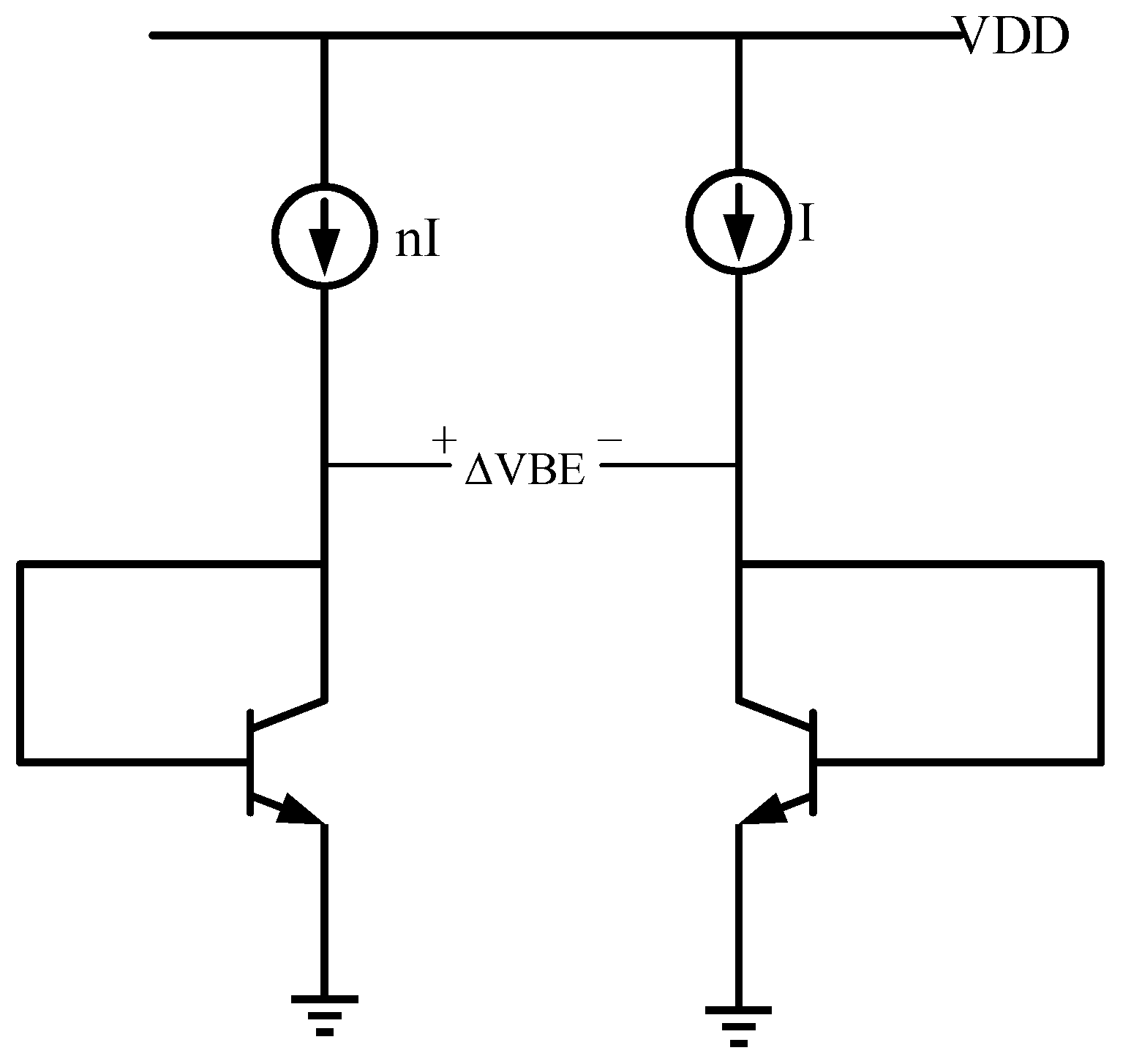
As shown in
Figure 1, if two identical transistors are biased with collector currents
nI and
I, respectively, then
Therefore, it can be seen that the temperature coefficient of the difference in
is a positive temperature coefficient:
It can be seen that this temperature coefficient is independent of temperature, which causes the temperature coefficient of the zero temperature coefficient voltage obtained by a certain ratio of the positive temperature coefficient voltage and the negative temperature coefficient voltage to change with temperature, resulting in a decrease in the output voltage accuracy.
3. Results Design of Curvature Compensation Reference Voltage Circuit
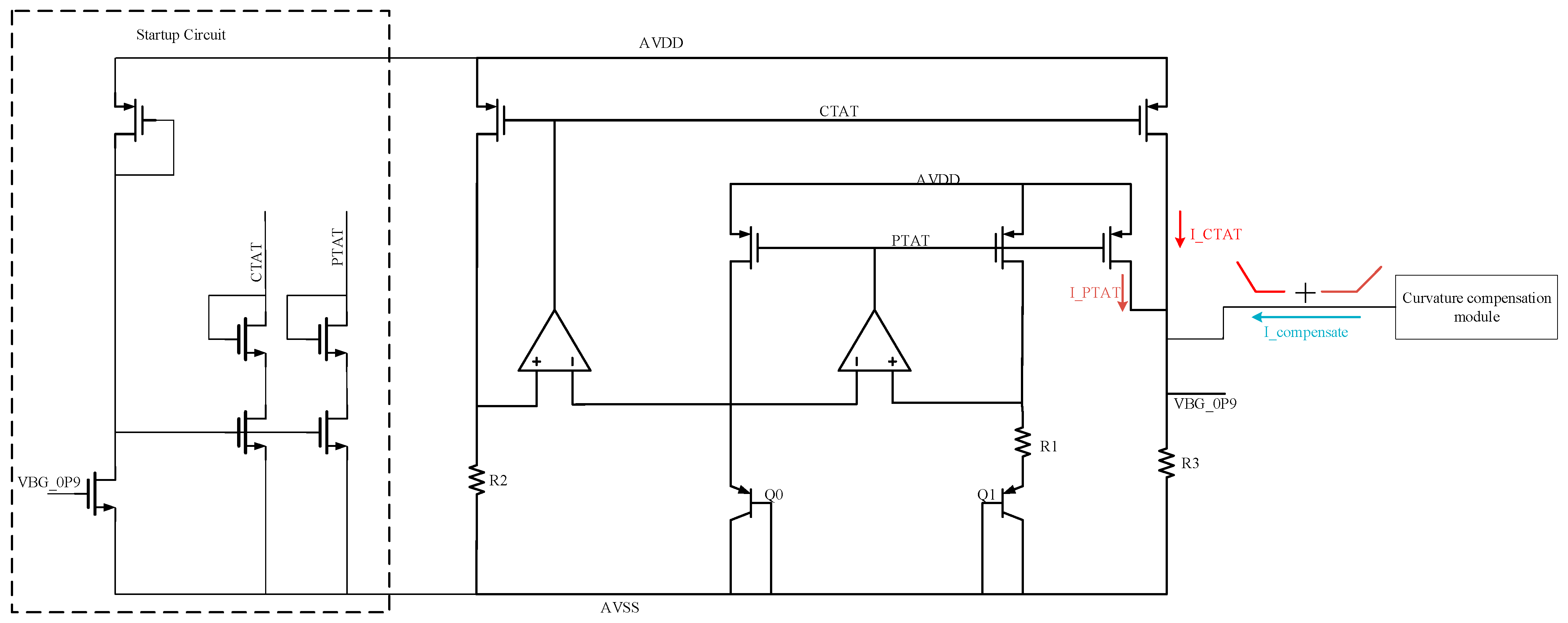
Figure 2 shows the top diagram of the proposed curvature compensation reference voltage circuit. In this design, analog voltage drain (AVDD) represents the analog supply voltage with a value of 1.8 V, and analog voltage source supply (AVSS) is the analog ground, with a voltage value of 0 V. Q0 and Q1 are transistors with a current mirror ratio of 1:8. R1, R2, and R3 are voltage divider resistors; their resistance values are 60.93 K, 615.286 K, and 441.487 K, respectively. The output voltage, denoted as a bandgap voltage reference of 0.9 V (VBG_0P9), is 0.9 V. Due to the clamping effect of the operational amplifier, the voltages at the positive and negative terminals of the operational amplifier are equal. At the same time, due to the effect of the current mirror, the current flowing through transistors Q0 and Q1 is equal, and the number of Q1 transistors in parallel is eight, so that the voltage difference between the positive and negative ends of resistor
R1 is the voltage difference between the two transistors, so the PTAT current is as follows:
Similarly, the CTAT current is generated by the transistor
VBE, and its current is as follows:
Similarly, the CTAT current is generated by the transistor
VBE, and its current is as follows:
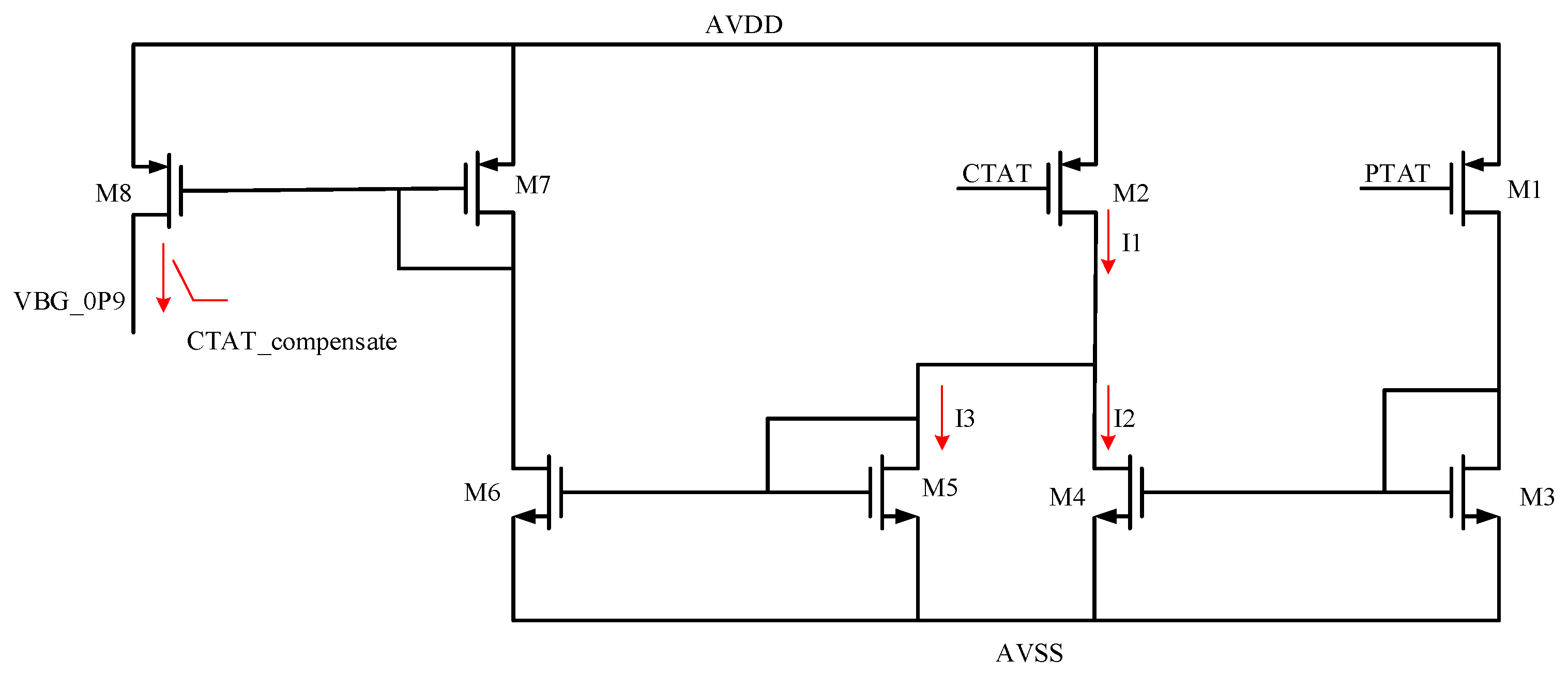
The low-temperature CTAT compensation circuit is shown in
Figure 3. In this circuit, the M1 and M2 transistors replicate the CTAT and PTAT currents, respectively, generated in
Figure 2, through the current mirror relationship. The current in the saturation region of the MOS transistor is given by the following equation:
where
is the electron mobility,
is the gate oxide capacitance,
is the width-to-length ratio of the transistor,
VGS is the gate-source voltage, and
Vth is the threshold voltage of the MOS transistor. Therefore, the replicated current is closely related to the width-to-length ratio of the MOS transistors.
As the PTAT current flows through M1 to M3, it is copied from M3 to M4 by Current Mirror 1 in a 1:1 ratio. From the current relationship, it follows that I1 = I2 + I3. Consequently, current will only flow through M5 if I1 is greater than I2. Since I1 is a current with a negative temperature coefficient and I2 has a positive temperature coefficient, current will only flow through M5 when the temperature is low enough for I1 to exceed I2. This current is then further mirrored through M6, M7, and M8 to produce the low-temperature compensation current.
In summary, the circuit generates the compensation current only under low-temperature conditions and does not produce any output current at high temperatures.
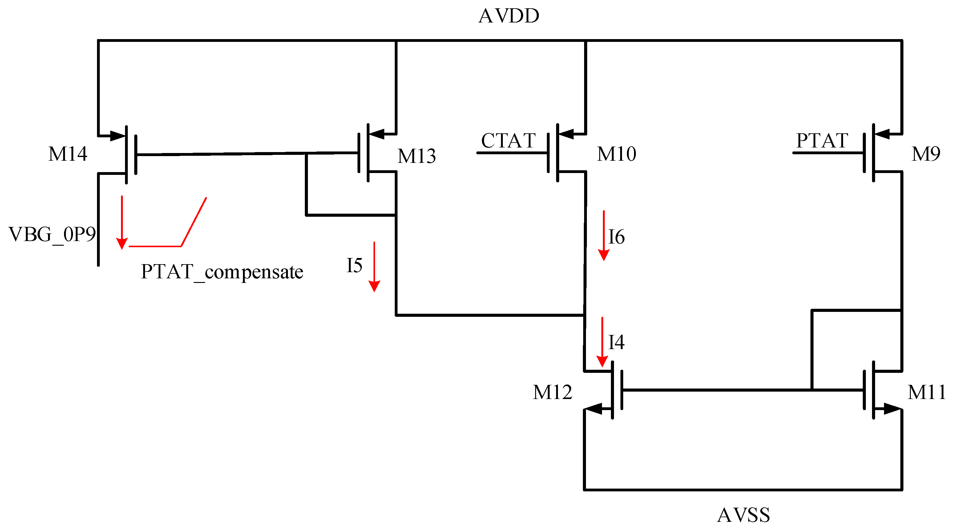
Figure 4 illustrates the high-temperature PTAT compensation circuit. Similar to the low-temperature compensation circuit, the PTAT current is replicated to I4 through the current mirrors M9, M11, and M12, while the CTAT current is replicated to I6 via the M10 current mirror. Based on the current relationship, we have I4 = I6 + I5. Therefore, current will only flow through the M13 transistor when the replicated PTAT current I4 exceeds I6.
Since I4 is a current with a positive temperature coefficient and I6 is a current with a negative temperature coefficient, I4 will be greater than I6 only at high temperatures. This condition allows current to flow through M13, and the high-temperature PTAT compensation current is generated through the replication of M14’s current mirror.
In summary, the circuit produces a current with a positive temperature coefficient only under high-temperature conditions, and the output current is zero at low temperatures.
The curvature compensation circuits depicted in
Figure 3 and
Figure 4 are designed to achieve segmented temperature compensation, addressing the unique challenges posed by varying temperature conditions. At low temperatures, the circuit compensates for the loss of curvature by utilizing the complementary to absolute temperature (CTAT) current. This approach effectively corrects inaccuracies that may arise in voltage reference outputs under cold conditions. Conversely, at high temperatures, the proportional to absolute temperature (PTAT) current is employed to mitigate deviations that occur in the high temperature range.
This dual compensation strategy significantly enhances the accuracy of the reference voltage compared to traditional voltage reference methods, which often struggle to maintain precision across diverse temperature environments. By specifically targeting the characteristics of both CTAT and PTAT currents, these circuits provide a more reliable and stable reference voltage, thus fulfilling the demanding requirements of various modern application scenarios.
As the need for precise voltage references continues to grow in sectors such as telecommunications, the automotive industry, and industrial control systems, the implementation of segmented temperature compensation becomes increasingly relevant. These advancements not only improve measurement accuracy but also contribute to the overall reliability and efficiency of electronic systems. Ultimately, the innovative designs represented in
Figure 3 and
Figure 4 exemplify a forward-thinking approach to voltage reference technology, ensuring that future applications can operate seamlessly across a wide range of environmental conditions.
4. Discussion Analysis of Experimental Results
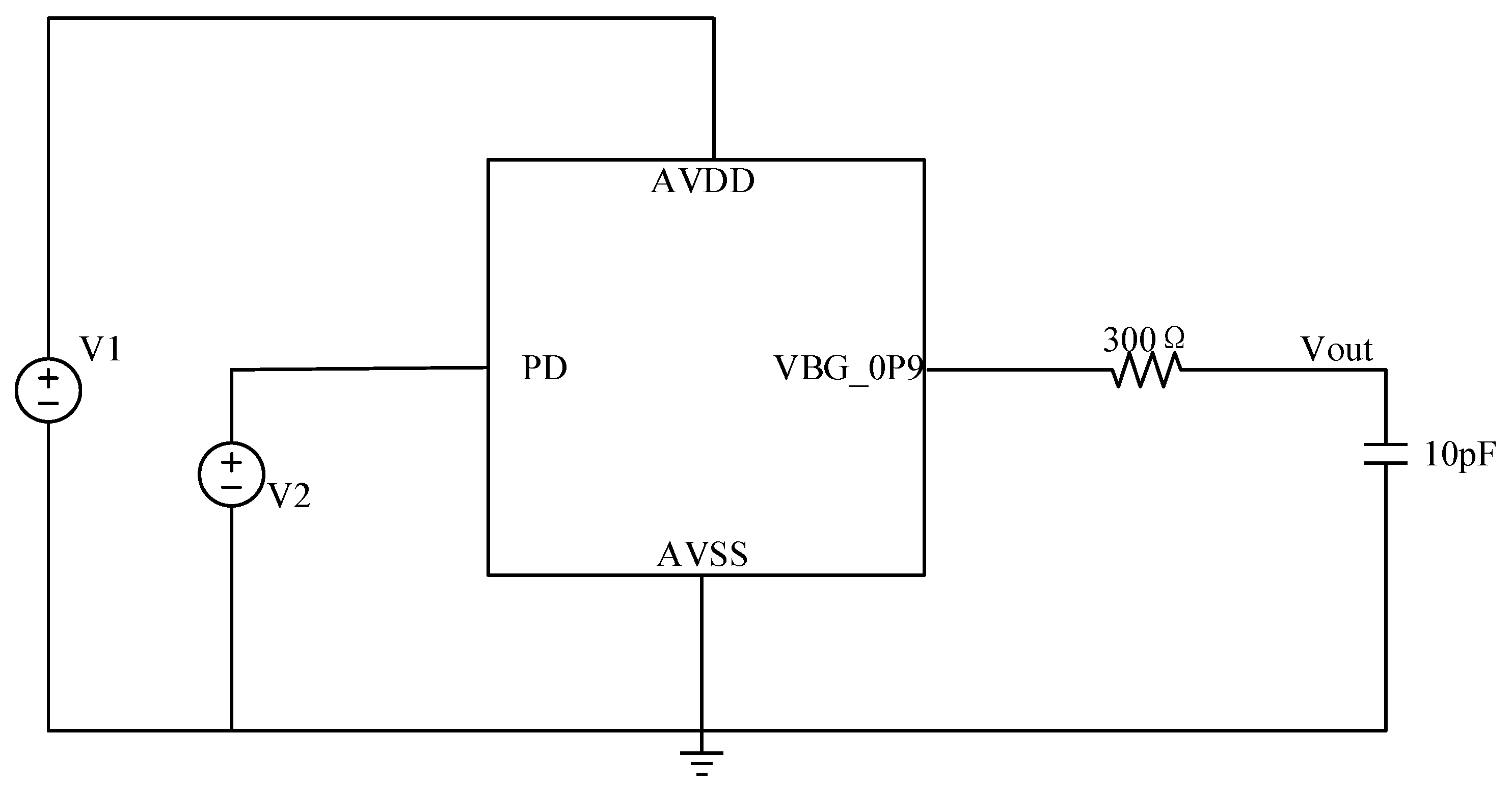
In this section, we will analyze the key data pertaining to the proposed reference voltage circuit. As shown in
Figure 5, the experimental verification schematic diagram includes several key components: AVDD, which is the analog voltage domain supplied by the V1 voltage source providing a 1.8 V voltage; PD, the switching input for the entire reference voltage circuit, where a low level turns it on, and a high level turns it off, provided by the V2 voltage source; and AVSS, the analog ground, which is connected to a low signal voltage. The VBG_0P9 generates the output voltage Vout through an RC filter. To verify the accuracy of the reference voltage circuit at various temperatures, the output voltage Vout is measured at different temperatures to assess the overall voltage accuracy.
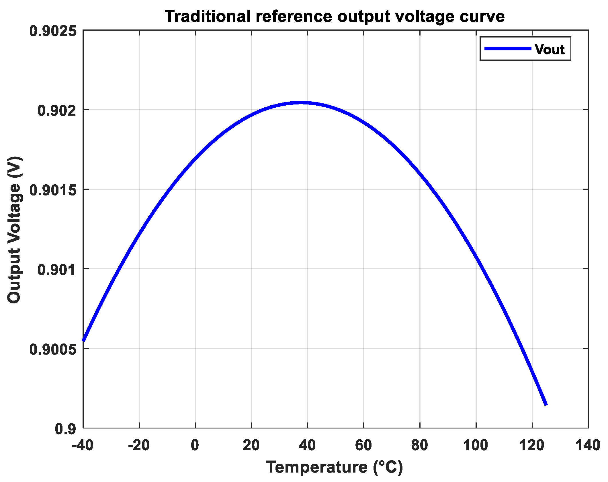
Figure 6 presents a simulation waveform of the output voltage from a traditional reference voltage circuit as temperature varies. It is apparent that changes in temperature lead to alterations in the negative temperature coefficient current curvature, resulting in deviations in the output of the reference voltage.
The temperature coefficient is a critical metric used to evaluate the accuracy of output voltage as temperature fluctuates. It quantifies how much the output voltage changes with temperature, providing insight into the circuit’s performance under varying environmental conditions. The mathematical expression for the temperature coefficient is given by Formula (10), where Formula (10) typically represents the rate of change in voltage per degree Celsius.
By understanding these dynamics, we can better assess the limitations of traditional circuits and the improvements offered by the proposed design.
According to Formula (11), the parts per million (PPM) [
23,
24] of the traditional reference voltage circuit is calculated to be 12.78. This reference voltage deviation arises from the loss of negative temperature coefficient curvature, which impacts measurement accuracy and system stability. The curvature compensation circuit structure proposed in this paper effectively addresses this loss, enabling the realization of a high-precision reference voltage generation circuit. By correcting the curvature across varying temperatures, this innovative design significantly improves voltage accuracy, making it well-suited for modern applications that demand enhanced reliability and performance.
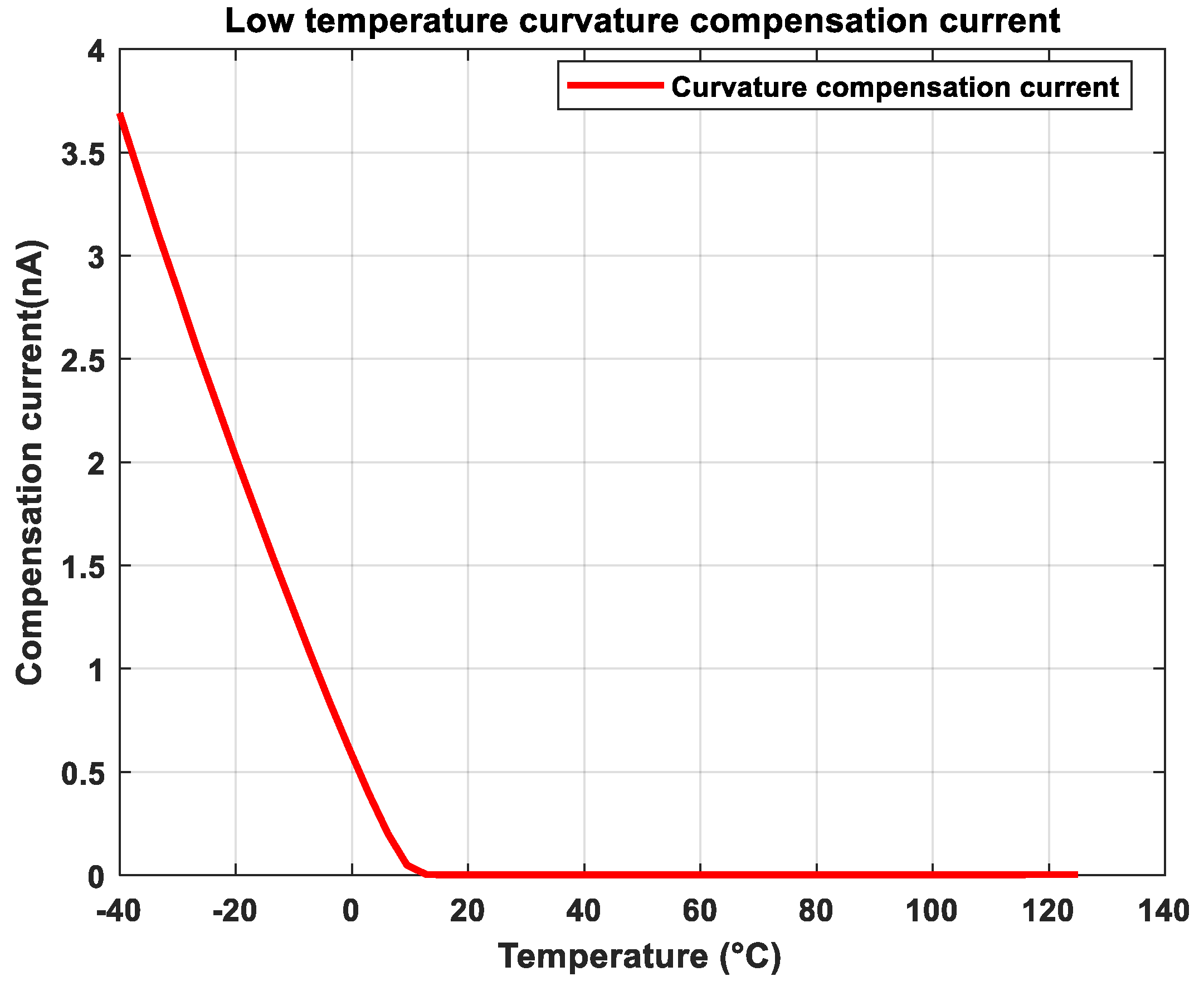
Figure 7 illustrates the curvature current waveform compensated by the circuit shown in
Figure 3. It is clear that the traditional output voltage waveform displays a positive temperature coefficient voltage due to the diminished negative temperature coefficient at low temperatures. To counteract this loss, a negative temperature coefficient current is introduced for compensation in the low temperature range. Importantly, this compensatory current is designed to become zero at temperatures outside the compensation range, effectively rectifying the curvature loss experienced at low temperatures. This mechanism not only enhances the accuracy of the reference voltage but also stabilizes the performance of the circuit across varying temperature conditions. By ensuring that the voltage output remains consistent, this approach improves the overall reliability of power systems, making it particularly valuable in applications where precision is paramount.
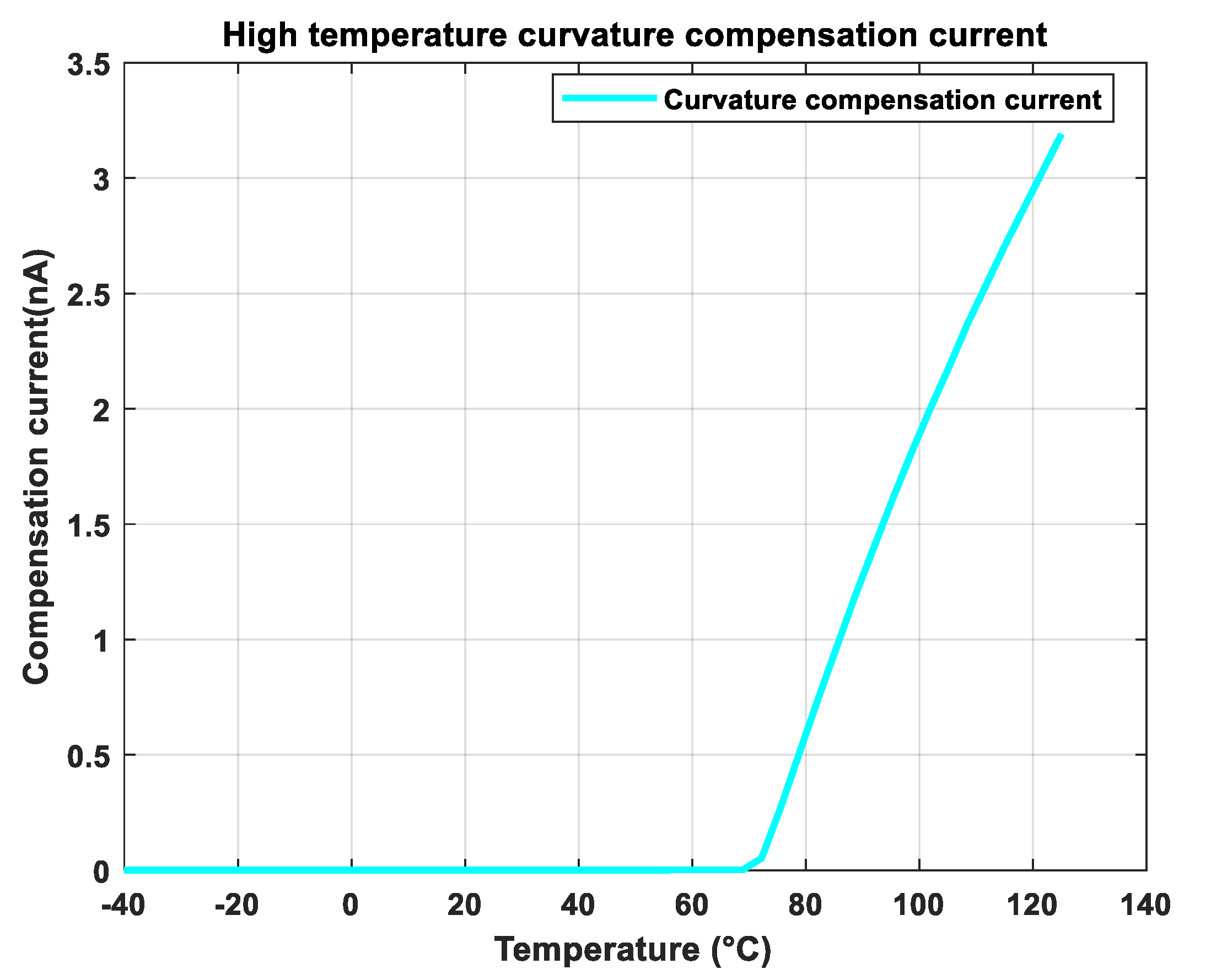
Figure 8 presents the high-temperature compensation current output curve for the circuit depicted in
Figure 4. It is evident that the traditional reference voltage experiences an increase in the negative temperature coefficient at elevated temperatures, leading to the output voltage curve exhibiting characteristics of negative temperature coefficient change. To effectively address this curvature loss, a positive temperature coefficient current is introduced at high temperatures. This compensatory current is essential for restoring voltage accuracy, ensuring that the reference voltage remains stable even under high-temperature conditions. By dynamically adjusting the output based on temperature fluctuations, this approach significantly enhances the reliability and performance of the voltage reference circuit. Such improvements are particularly important for applications in harsh environments where precision and stability are critical, ultimately contributing to the overall safety and efficiency of power systems.
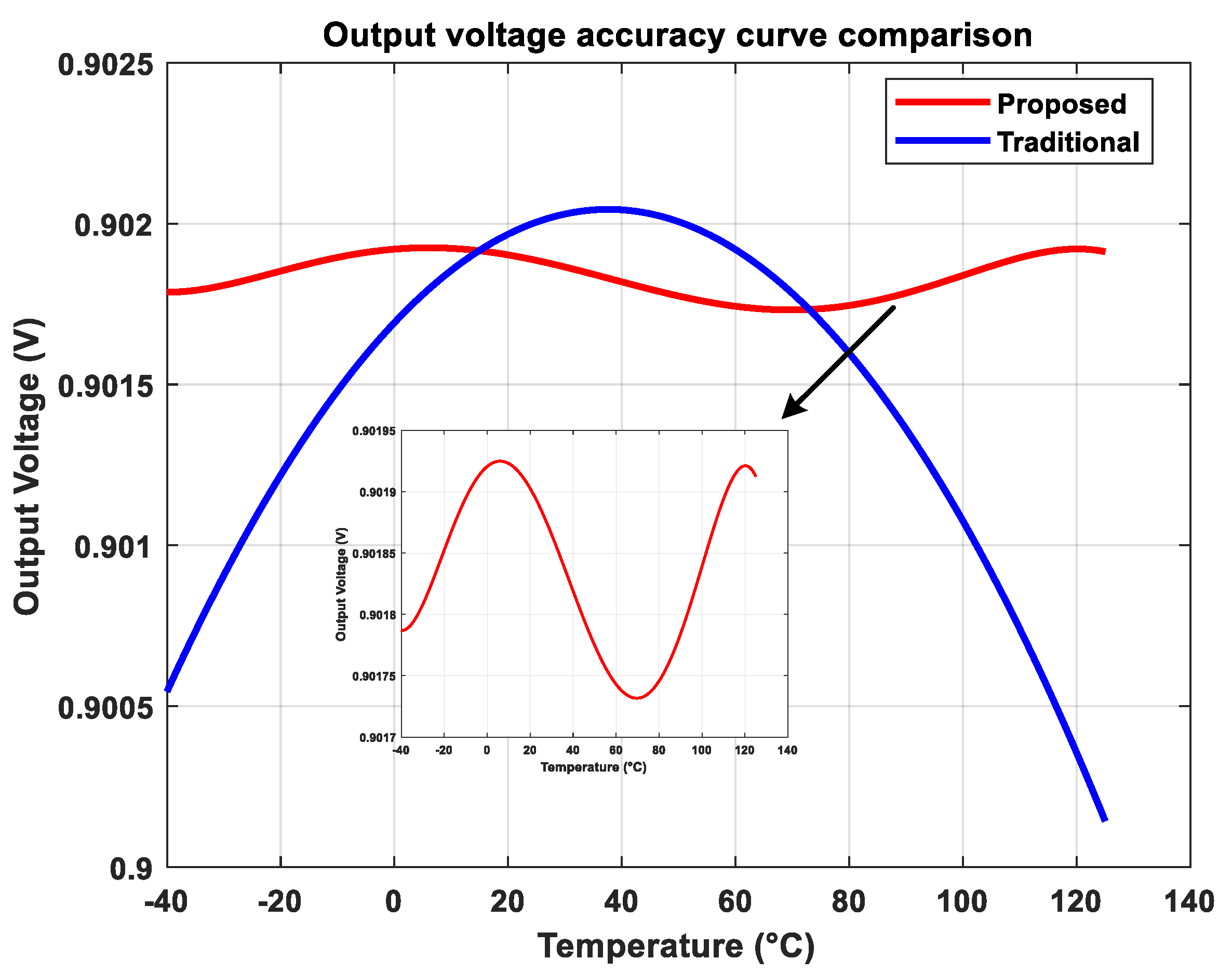
Figure 9 provides a comparison of the output voltages between the proposed reference voltage circuit and a traditional reference voltage circuit. The results clearly indicate that the implementation of the proposed curvature compensation circuit significantly enhances the accuracy of the output voltage. This improvement effectively addresses the curvature loss problem that arises from the temperature coefficient of the negative temperature coefficient current, which varies with temperature. The experimental results demonstrate that the output accuracy of the newly designed curvature compensated reference voltage circuit reaches an impressive level of just 3.34 ppm.
This level of precision is a substantial advancement over traditional methods, making the proposed circuit particularly advantageous for applications that require stringent voltage stability and accuracy. Such enhancements not only optimize performance in varying thermal conditions but also ensure greater reliability in critical electronic systems. As demands for precision increase in industries such as telecommunications, the automotive industry, and industrial automation, the advancements presented by this curvature compensation technique will play a crucial role in the future development of high-performance voltage reference circuits.
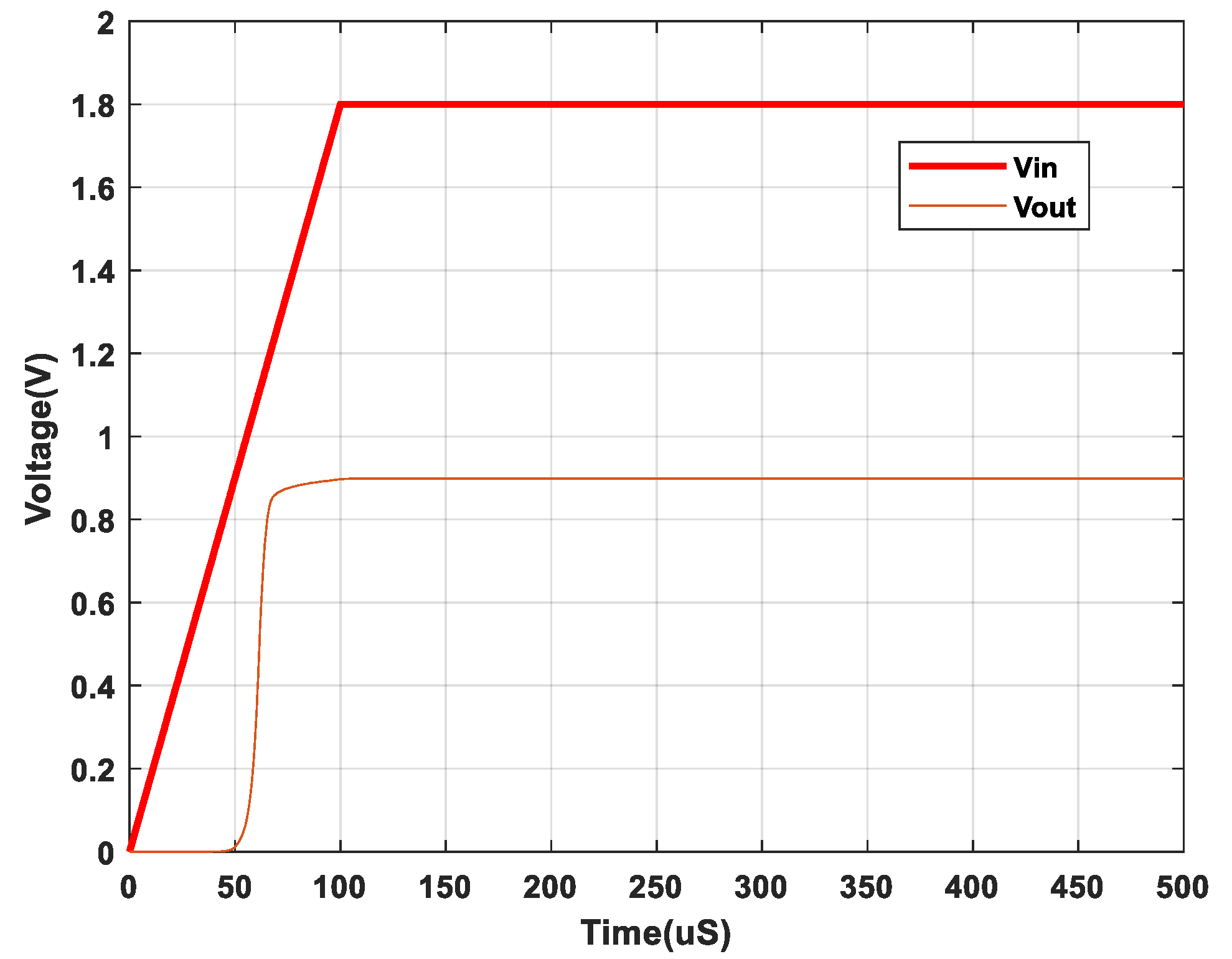
The transient power-on process of the proposed voltage reference circuit is illustrated in
Figure 10 below. Here, Vin represents the input voltage of 1.8 V, while Vout denotes the output voltage of the proposed reference circuit. As shown, under typical operating conditions, the circuit achieves a stable output voltage of 0.9 V within 100 µs after Vin is powered on.
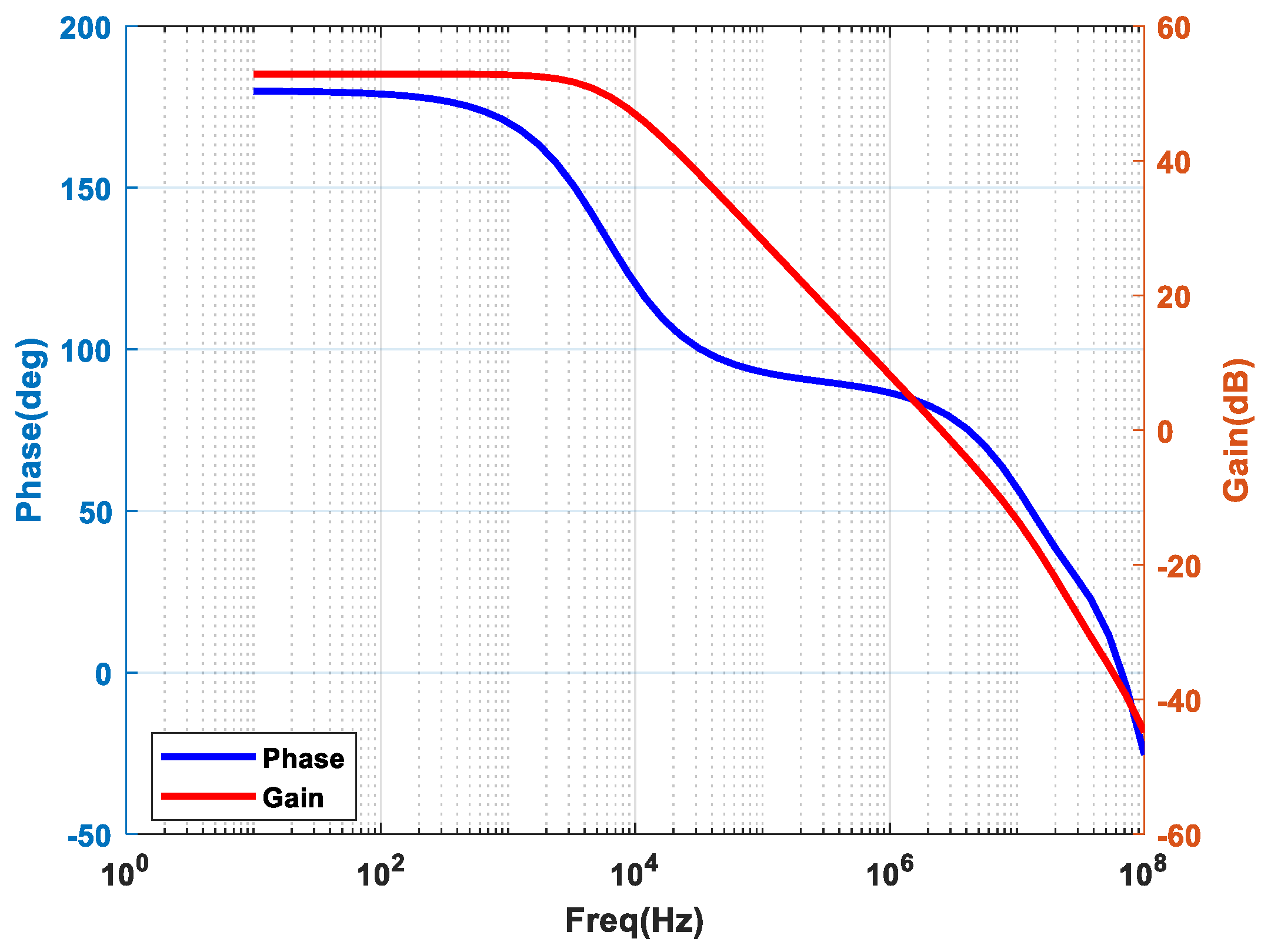
Figure 11 shows the frequency response results of the proposed reference voltage circuit. It can be seen that the loop phase margin of the proposed reference voltage circuit is 80.74 deg, which indicates that the proposed reference voltage circuit has sufficient phase margin to avoid output voltage oscillation and instability during startup.


 and
and 