
High Efficiency Dual-Active-Bridge Converter with Triple-Phase-Shift Control for Battery Charger of Electric Vehicles


 , , , and
Abstract
1. Introduction
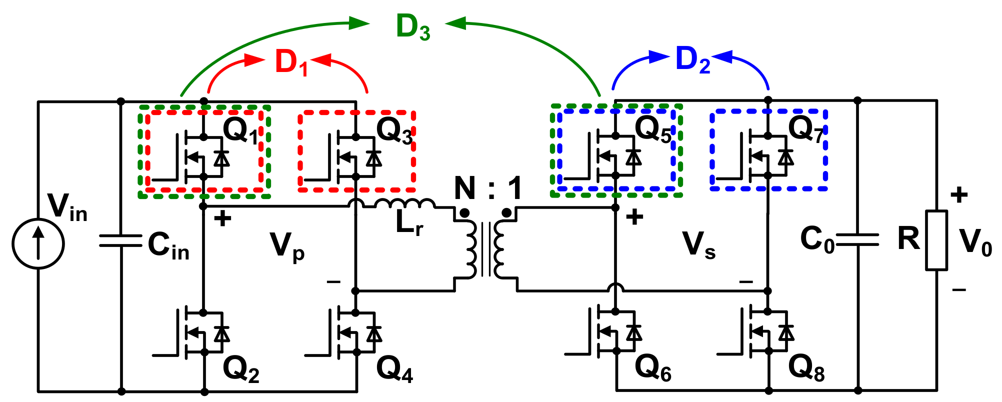
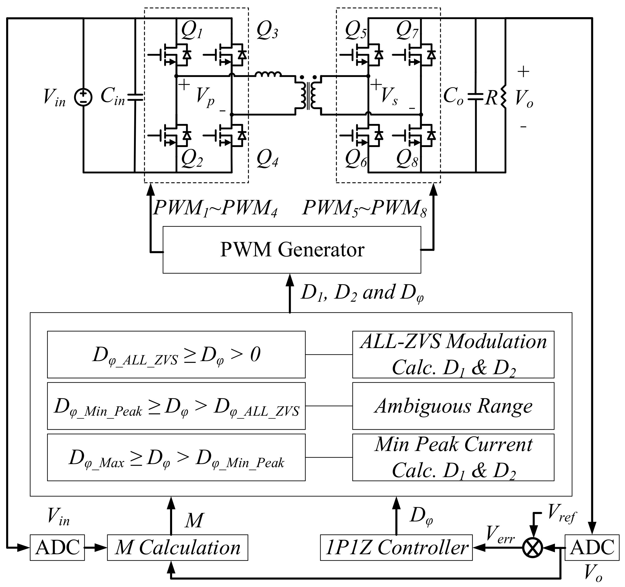
2. Dual-Active-Bridge Converter
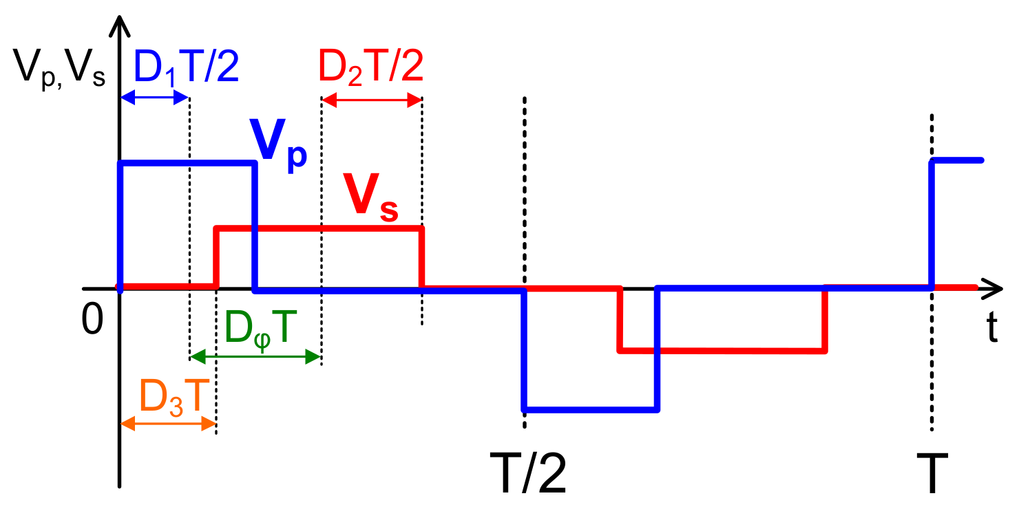
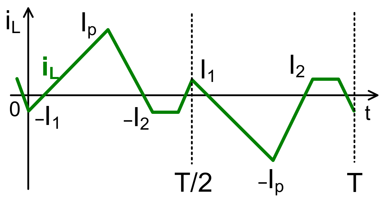
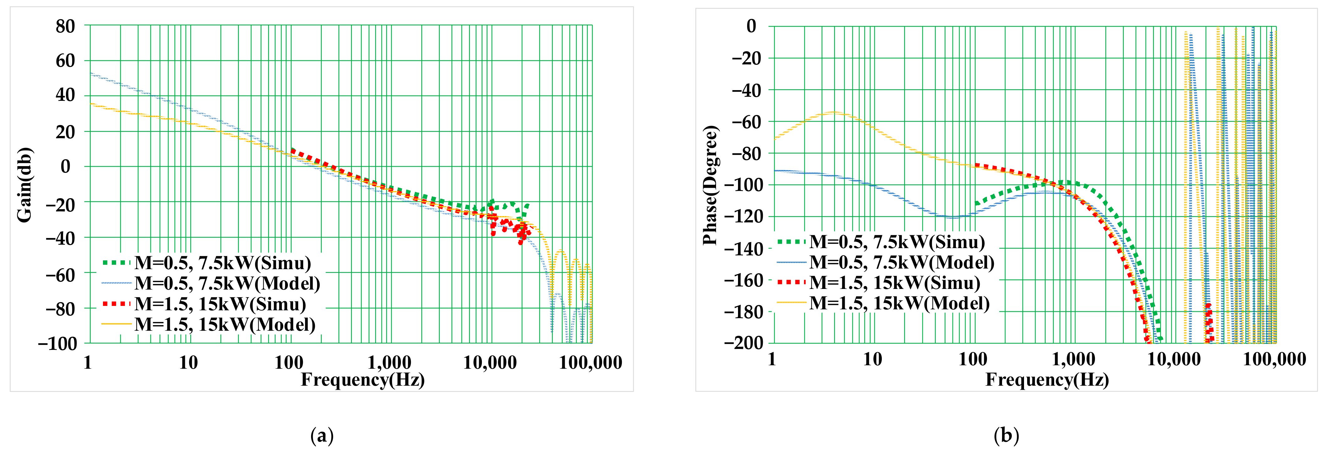
3. Small-Signal Modeling and Analysis of TPS
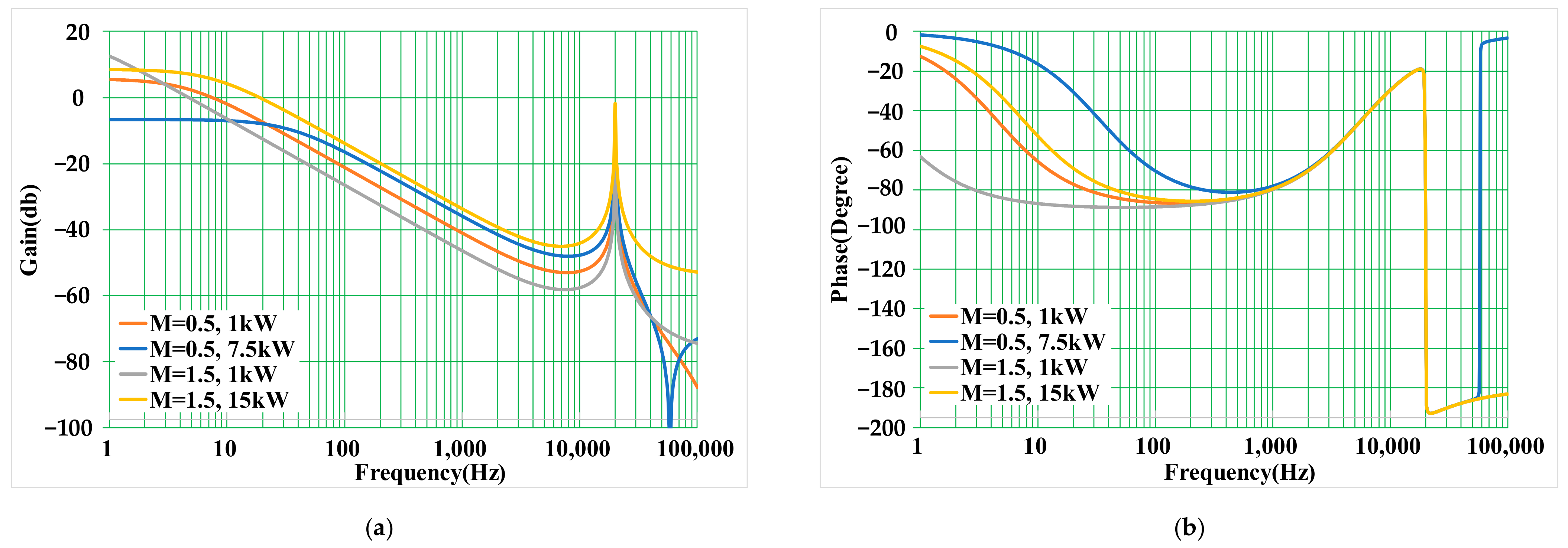
4. Control Loop Design Consideration
5. Experimental Verifications
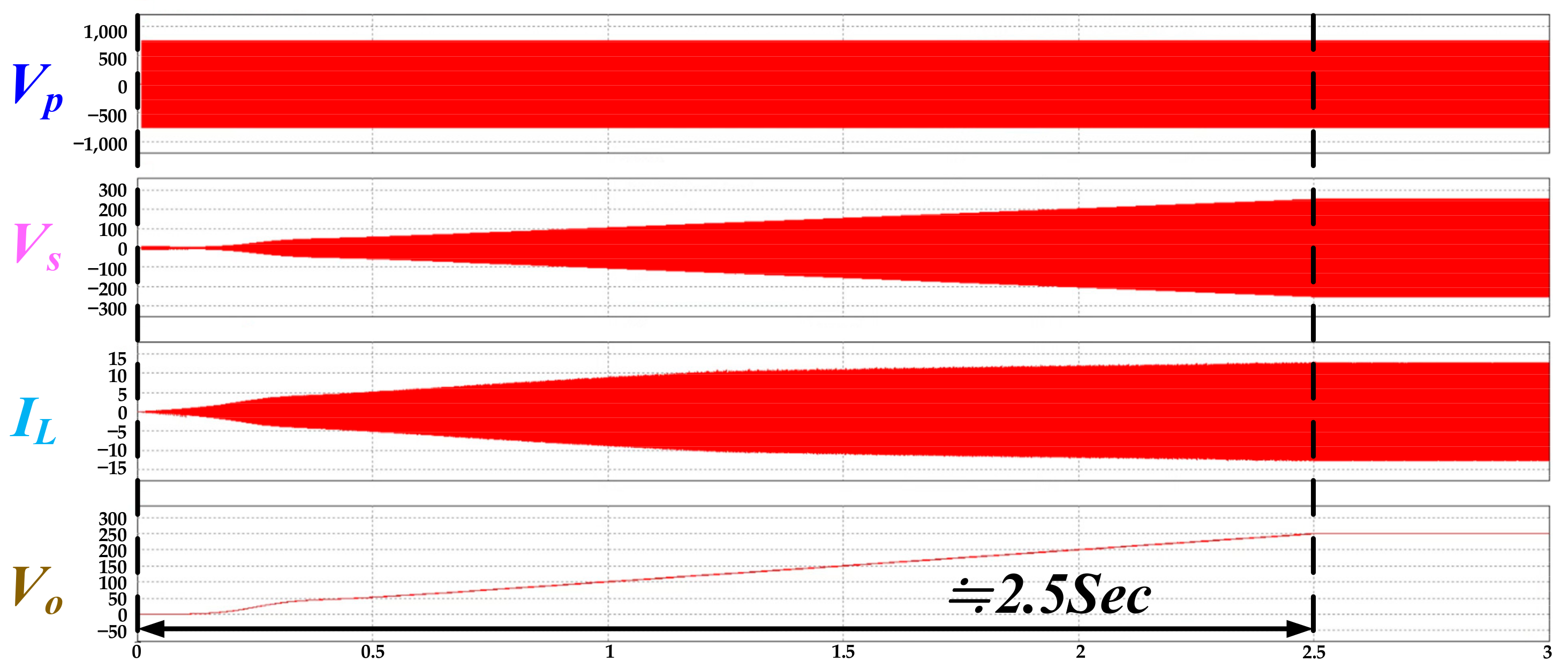
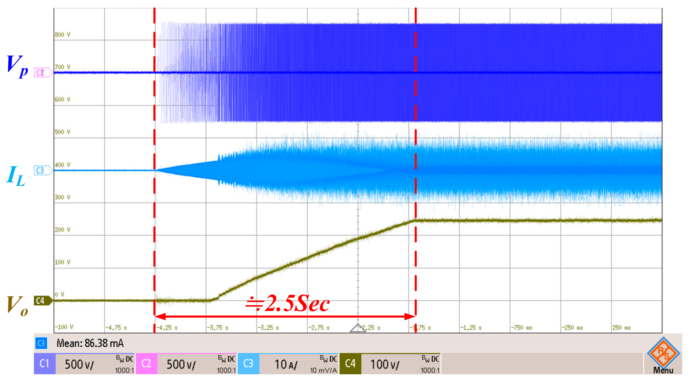
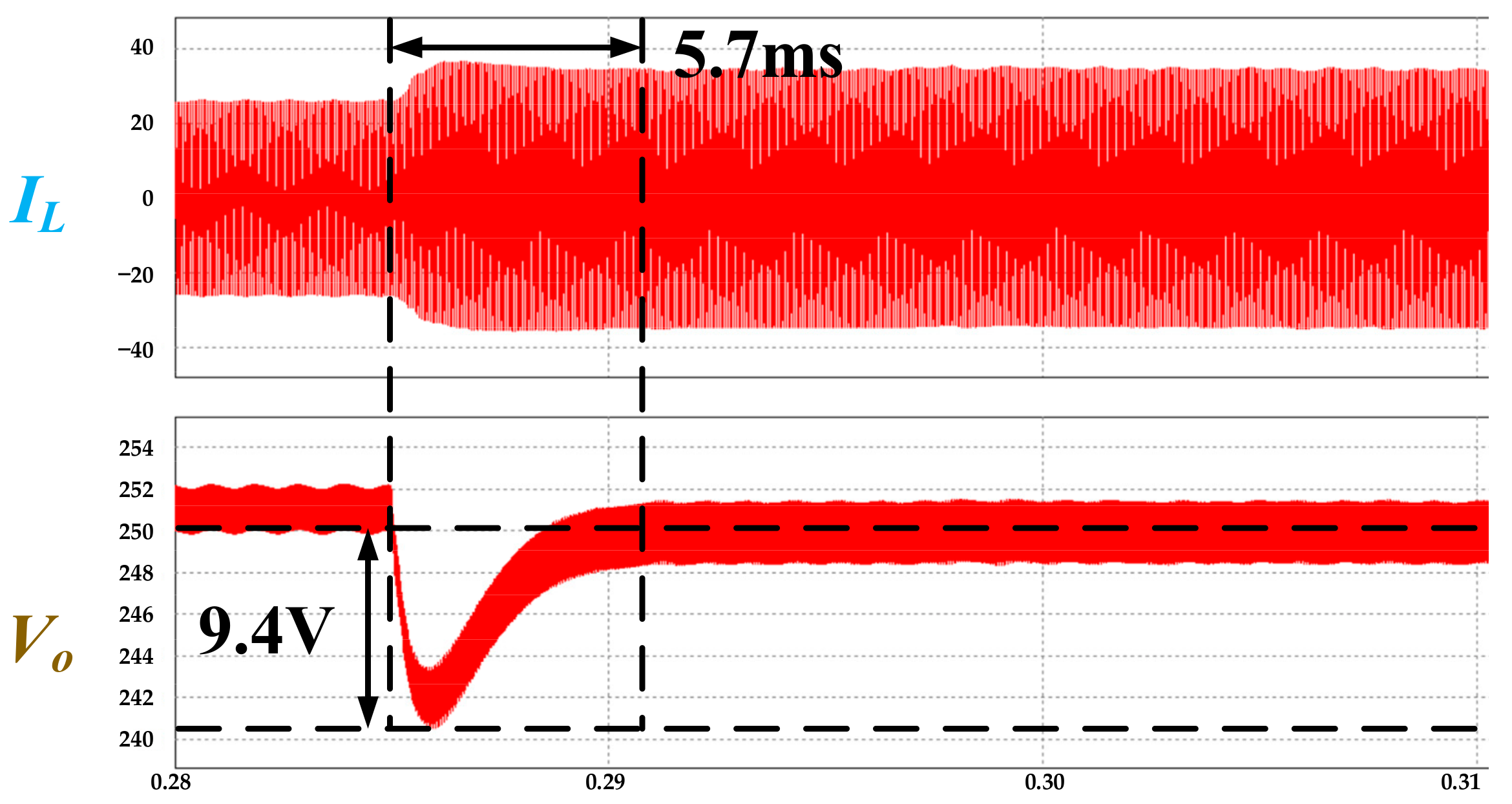
5.1. Result of Soft-Start and Transient Response
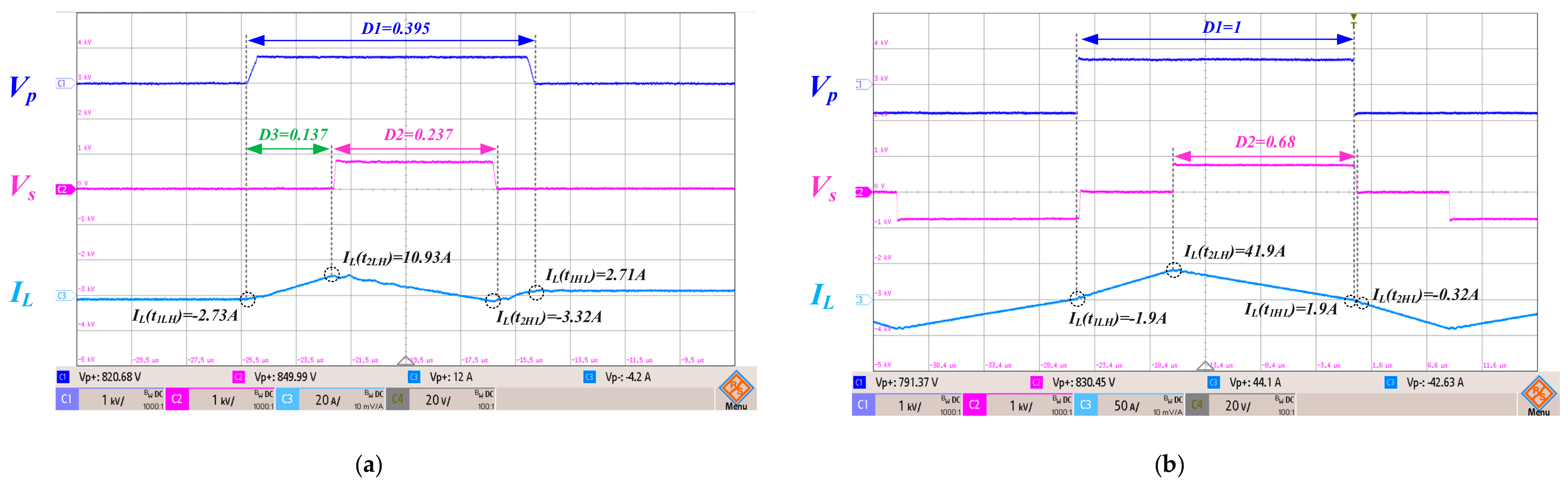
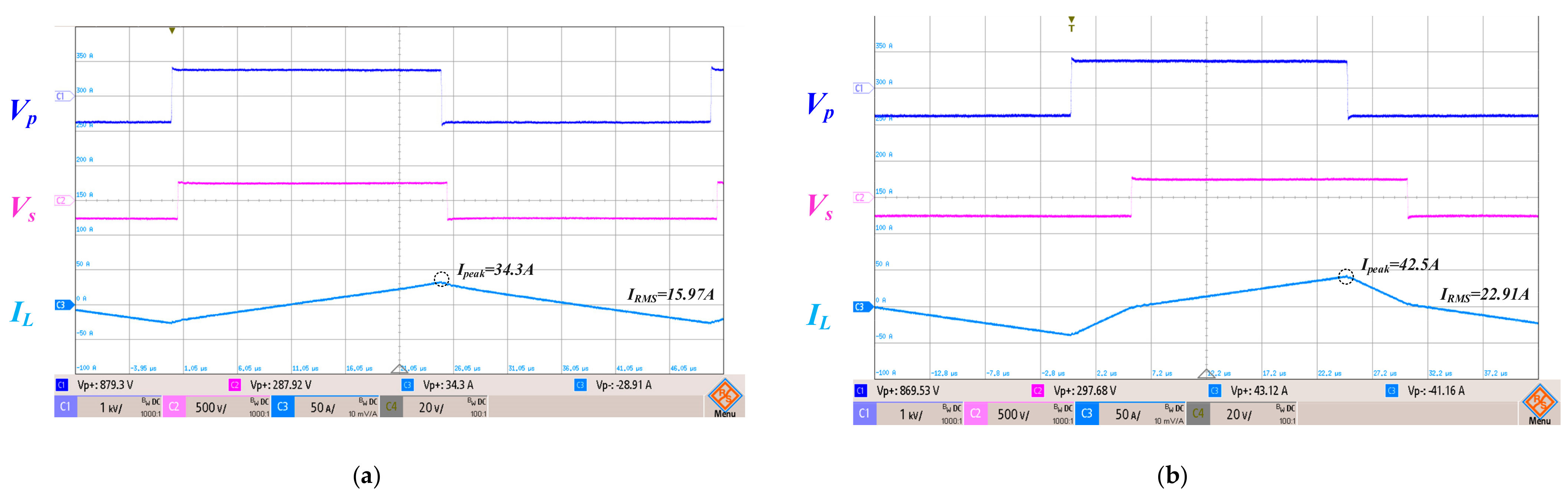
5.2. Switching Waveform Comparison of SPS and TPS
5.3. Efficiency Comparison
6. Conclusions
Author Contributions
Funding
Data Availability Statement
Conflicts of Interest
Appendix A
References
- Acharige, S.S.G.; Haque, M.E.; Arif, M.T.; Hosseinzadeh, N.; Hasan, K.N.; Oo, A.M.T. Review of Electric Vehicle Charging Technologies, Standards, Architectures, and Converter Configurations. IEEE Access 2023, 11, 41218–41255. [Google Scholar] [CrossRef]
- Safayatullah, M.; Elrais, M.T.; Ghosh, S.; Rezaii, R.; Batarseh, I. A Comprehensive Review of Power Converter Topologies and Control Methods for Electric Vehicle Fast Charging Applications. IEEE Access 2022, 10, 40753–40793. [Google Scholar] [CrossRef]
- Shurrab, M.; Singh, S.; Otrok, H.; Mizouni, R.; Khadkikar, V.; Zeineldin, H. An Efficient Vehicle-to-Vehicle (V2V) Energy Sharing Framework. IEEE Internet Things J. 2022, 9, 5315–5328. [Google Scholar] [CrossRef]
- Haque, M.M.; Wolfs, P.; Alahakoon, S.; Sturmberg, B.C.P.; Nadarajah, M.; Zare, F. DAB Converter with Q Capability for BESS/EV Applications to Allow V2H/V2G Services. IEEE Trans. Ind. Appl. 2022, 58, 468–480. [Google Scholar] [CrossRef]
- Zayed, O.; Elezab, A.; Abuelnaga, A.; Narimani, M. A Dual-Active Bridge Converter with a Wide Output Voltage Range (200–1000 V) for Ultrafast DC-Connected EV Charging Stations. IEEE Trans. Transp. Electrif. 2023, 9, 3731–3741. [Google Scholar] [CrossRef]
- Assadi, S.A.; Matsumoto, H.; Moshirvaziri, M.; Nasr, M.; Zaman, M.S.; Trescases, O. Active saturation mitigation in high-density dual-active-bridge DC–DC converter for on-board EV charger applications. IEEE Trans. Power Electron. 2019, 35, 4376–4387. [Google Scholar] [CrossRef]
- Choi, H.-J.; Jung, J.-H. Practical design of dual active bridge converter as isolated bi-directional power interface for solid state transformer applications. J. Electr. Eng. Technol. 2016, 11, 1265–1273. [Google Scholar] [CrossRef]
- Fontes, G.; Turpin, C.; Astier, S.; Meynard, T.A. Interactions between fuel cells and power converters: Influence of current harmonics on a fuel cell stack. IEEE Trans. Power Electron. 2007, 22, 670–678. [Google Scholar] [CrossRef]
- Ehsani, M.; Singh, K.V.; Bansal, H.O.; Mehrjardi, R.T. State of the Art and Trends in Electric and Hybrid Electric Vehicles. Proc. IEEE 2021, 109, 967–984. [Google Scholar] [CrossRef]
- Tu, H.; Feng, H.; Srdic, S.; Lukic, S. Extreme Fast Charging of Electric Vehicles: A Technology Overview. IEEE Trans. Transp. Electrif. 2019, 5, 861–878. [Google Scholar] [CrossRef]
- Schmid, J.; Strauss, P.; Hatziargyriou, N.; Akkermans, H.; Buchholz, B.; Van Oostvoorn, F.; Scheepers, M.; Reyero, R.; Chadjivassiliadis, J. Towards Smart Power Networks: Lessons Learned from European Research FP5 Projects; European Commission Directorate-General for Research Information and Communication Unit: Brussels, Belgium, 2005.
- Barone, G.; Brusco, G.; Burgio, A.; Motta, M.; Menniti, D.; Pinnarelli, A.; Sorrentino, N. A dual active bridge dc-dc converter for application in a smart user network. In Proceedings of the 2014 Australasian Universities Power Engineering Conference (AUPEC), Perth, WA, Australia, 28 September–1 October 2014; pp. 1–5. [Google Scholar]
- Manez, K.T. Advances in bidirectional DC-DC converters for future energy systems. Ph.D. Thesis, Technical University of Denmark, Lyngby, Denmark, 2018. [Google Scholar]
- Xue, L.; Shen, Z.; Boroyevich, D.; Mattavelli, P.; Diaz, D. Dual active bridge-based battery charger for plug-in hybrid electric vehicle with charging current containing low frequency ripple. IEEE Trans. Power Electron. 2015, 30, 7299–7307. [Google Scholar] [CrossRef]
- Mathew, A.; Prasad, U.R.; Madhu, G.M.; Naik, N.; Vyjayanthi, C.; Subudhi, B. Performance Analysis of a Dual Active Bridge Converter in EV Charging Applications. In Proceedings of the 2022 International Conference for Advancement in Technology (ICONAT), Goa, India, 21–22 January 2022; pp. 1–6. [Google Scholar]
- Bai, H.; Mi, C. Eliminate Reactive Power and Increase System Efficiency of Isolated Bidirectional Dual-Active-Bridge DC–DC Converters Using Novel Dual-Phase-Shift Control. IEEE Trans. Power Electron. 2008, 23, 2905–2914. [Google Scholar] [CrossRef]
- Feng, B.; Wang, Y.; Man, J. A novel dual-phase-shift control strategy for dual-active-bridge DC-DC converter. In Proceedings of the IECON 2014—40th Annual Conference of the IEEE Industrial Electronics Society, Dallas, TX, USA, 29 October–1 November 2014; pp. 4140–4145. [Google Scholar]
- Shao, S.; Jiang, M.; Ye, W.; Li, Y.; Zhang, J.; Sheng, K. Optimal Phase-Shift Control to Minimize Reactive Power for a Dual Active Bridge DC–DC Converter. IEEE Trans. Power Electron. 2019, 34, 10193–10205. [Google Scholar] [CrossRef]
- Zhao, B.; Song, Q.; Liu, W.; Sun, Y. Overview of Dual-Active-Bridge Isolated Bidirectional DC–DC Converter for High-Frequency-Link Power-Conversion System. IEEE Trans. Power Electron. 2014, 29, 4091–4106. [Google Scholar] [CrossRef]
- Zhao, B.; Yu, Q.; Sun, W. Extended-Phase-Shift Control of Isolated Bidirectional DC–DC Converter for Power Distribution in Microgrid. IEEE Trans. Power Electron. 2012, 27, 4667–4680. [Google Scholar] [CrossRef]
- Huang, J.; Wang, Y.; Li, Z.; Lei, W. Unified Triple-Phase-Shift Control to Minimize Current Stress and Achieve Full Soft-Switching of Isolated Bidirectional DC–DC Converter. IEEE Trans. Ind. Electron. 2016, 63, 4169–4179. [Google Scholar] [CrossRef]
- Middlebrook, R.D.; Cuk, S. A general unified approach to modelling switching-converter power stages. In Proceedings of the 1976 IEEE Power Electronics Specialists Conference, Cleveland, OH, USA, 8–10 June 1976; pp. 18–34. [Google Scholar]
- Das, D.; Mishra, S.; Singh, B. Design Architecture for Continuous-Time Control of Dual Active Bridge Converter. IEEE J. Emerg. Sel. Top. Power Electron. 2021, 9, 3287–3295. [Google Scholar] [CrossRef]
- Hiltunen, J.; Väisänen, V.; Juntunen, R.; Silventoinen, P. Variable-frequency phase shift modulation of a dual active bridge converter. IEEE Trans. Power Electron. 2015, 30, 7138–7148. [Google Scholar] [CrossRef]
- van Hoek, H.; Neubert, M.; De Doncker, R.W. Enhanced modulation strategy for a three-phase dual active bridge—Boosting efficiency of an electric vehicle converter. IEEE Trans. Power Electron. 2013, 28, 5499–5507. [Google Scholar] [CrossRef]
- Krismer, F.; Kolar, J.W. Accurate power loss model derivation of a high-current dual active bridge converter for an automotive application. IEEE Trans. Ind. Electron. 2009, 57, 881–891. [Google Scholar] [CrossRef]
- Calderon, C.; Barrado, A.; Rodriguez, A.; Alou, P.; Lazaro, A.; Fernandez, C.; Zumel, P. General analysis of switching modes in a dual active bridge with triple phase shift modulation. Energies 2018, 11, 2419. [Google Scholar] [CrossRef]
- Bacha, S.; Munteanu, I.; Bratcu, A.I. Power electronic converters modeling and control. Adv. Textb. Control Signal Process. 2014, 454, 454. [Google Scholar]
- Iqbal, M.T.; Maswood, A.I. An explicit discrete-time large-and small-signal modeling of the dual active bridge DC–DC converter based on the time scale methodology. IEEE J. Emerg. Sel. Top. Ind. Electron. 2021, 2, 545–555. [Google Scholar] [CrossRef]
- Safayatullah, M.; Batarseh, I. Small signal model of dual active bridge converter for multi-phase shift modulation. In Proceedings of the 2020 IEEE Energy Conversion Congress and Exposition (ECCE), Detroit, MI, USA, 11–15 October 2020; pp. 5960–5965. [Google Scholar]
- Bu, Q.; Wen, H. Triple-phase-shifted bidirectional full-bridge converter with wide range zvs. In Proceedings of the 2018 IEEE International Conference on Power Electronics, Drives and Energy Systems (PEDES), Chennai, India, 18–21 December 2018; pp. 1–6. [Google Scholar]
- Chen, Y.-H.; Huang, T.-W.; Kuo, S.-H.; Chang, Y.-C.; Chiu, H.-J.; Bachman, S.; Jasiński, M. Dual-Active-Bridge Converter with Triple Phase Shift Control for a Wide Operating Voltage Range. In Proceedings of the 2023 11th International Conference on Power Electronics and ECCE Asia (ICPE 2023-ECCE Asia), Jeju, Republic of Korea, 22–25 May 2023; pp. 1752–1755. [Google Scholar]
- Qin, H.; Kimball, J.W. Generalized average modeling of dual active bridge DC–DC converter. IEEE Trans. Power Electron. 2011, 27, 2078–2084. [Google Scholar]
- Sanders, S.R.; Noworolski, J.M.; Liu, X.Z.; Verghese, G.C. Generalized averaging method for power conversion circuits. IEEE Trans. Power Electron. 1991, 6, 251–259. [Google Scholar] [CrossRef]


| Case 1 | Case 2 | |
|---|---|---|
| M | M < 1 (Case 2) | M > 1 (Case 1) | |
|---|---|---|---|
| Power Range | |||
| Switches | ZVS Conditions |
|---|---|
| Q1 | |
| Q3 | |
| Q5 | |
| Q7 |
| Parameters | Value |
|---|---|
| Switching Frequency (fs) | 20 kHz |
| Input Voltage (Vin) | 750 V |
| Load Resistance (R) | 62.5 Ω (M = 0.5, 1 kW) |
| 8.33 Ω (M = 0.5, 7.5 kW) | |
| 562.5 Ω (M = 1.5, 1 kW) | |
| 37.5 Ω (M = 1.5, 15 kW) | |
| Output Capacitance (Co) | 560 μF |
| Output Capacitor ESR (rc) | 50 mΩ |
| Series Inductance (Lt) | 164 μH |
| Circuit DCR (Rt) | 55 mΩ |
| Turns Ratio (N) | 1.55:1 |
| PWM Modulation Gain (Fm(s)) | 1/3000 |
| Parameters | Value |
|---|---|
| Switching Frequency (fs) | 20 kHz |
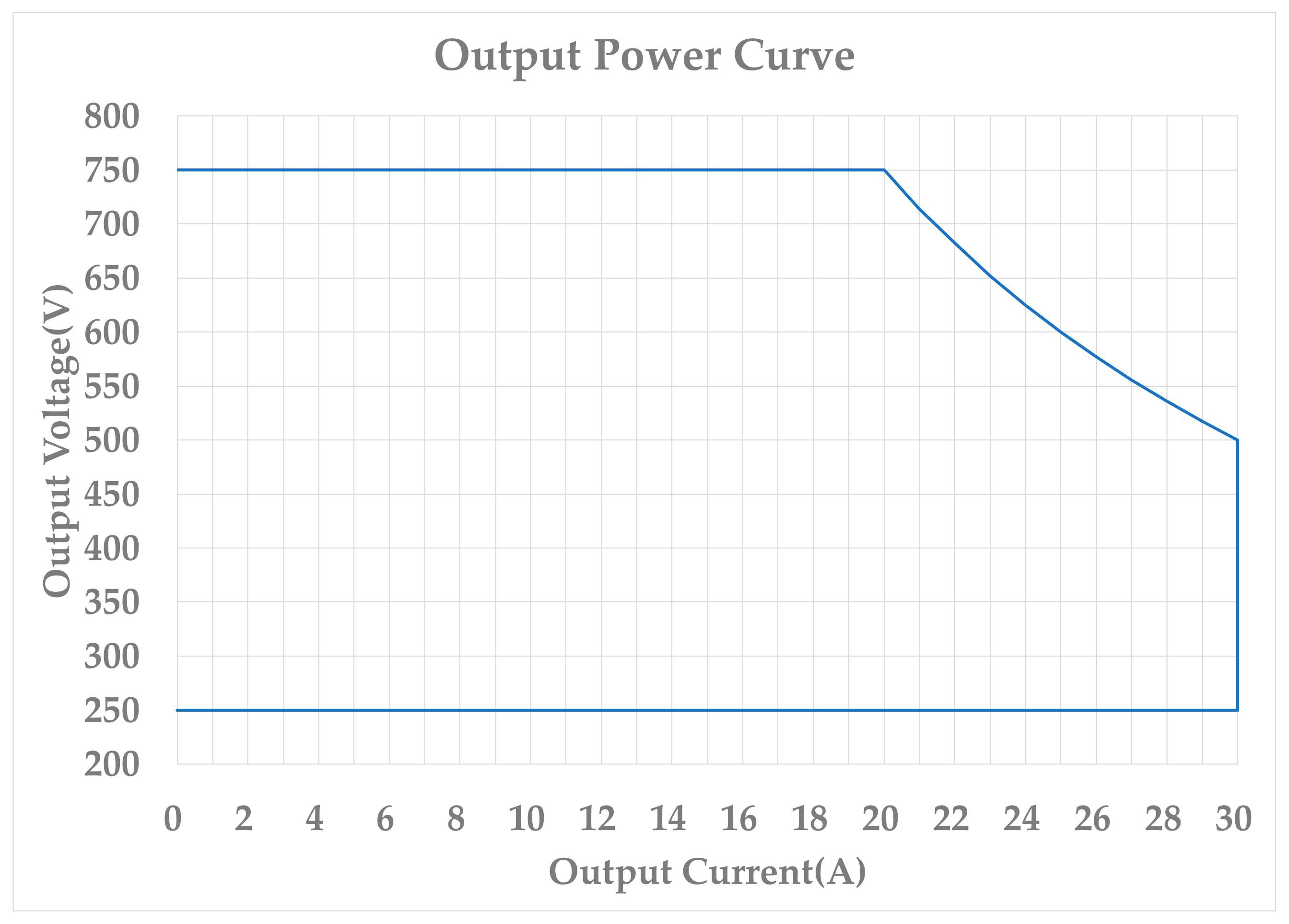
| Input Voltage (Vin) | 750 V |
| Output Voltage (Vo) | 250 V~750 V |
| Maximum Output Power (Po) | 15 kW |
| Maximum Output Current (Io) | 30 A (Constant Current) |
| Output Capacitance (Co) | 560 μF |
| Output Capacitor ESR (rc) | 50 mΩ |
| Series Inductance (Lt) | 164 μH |
| MOSFET Output Capacitance (Coss) | 550 pF (Infineon FF23MR12W1M1_B11) |
| Turns Ratio (N) | 1.55:1 |
Disclaimer/Publisher’s Note: The statements, opinions and data contained in all publications are solely those of the individual author(s) and contributor(s) and not of MDPI and/or the editor(s). MDPI and/or the editor(s) disclaim responsibility for any injury to people or property resulting from any ideas, methods, instructions or products referred to in the content. |
© 2024 by the authors. Licensee MDPI, Basel, Switzerland. This article is an open access article distributed under the terms and conditions of the Creative Commons Attribution (CC BY) license (https://creativecommons.org/licenses/by/4.0/).
Share and Cite
Kuo, S.-h.; Chiu, H.-J.; Chiang, C.-W.; Huang, T.-W.; Chang, Y.-C.; Bachman, S.; Piasecki, S.; Jasinski, M.; Turzyński, M. High Efficiency Dual-Active-Bridge Converter with Triple-Phase-Shift Control for Battery Charger of Electric Vehicles. Energies 2024, 17, 354. https://doi.org/10.3390/en17020354
Kuo S-h, Chiu H-J, Chiang C-W, Huang T-W, Chang Y-C, Bachman S, Piasecki S, Jasinski M, Turzyński M. High Efficiency Dual-Active-Bridge Converter with Triple-Phase-Shift Control for Battery Charger of Electric Vehicles. Energies. 2024; 17(2):354. https://doi.org/10.3390/en17020354
Chicago/Turabian StyleKuo, Shih-hao, Huang-Jen Chiu, Che-Wei Chiang, Ta-Wei Huang, Yu-Chen Chang, Serafin Bachman, Szymon Piasecki, Marek Jasinski, and Marek Turzyński. 2024. "High Efficiency Dual-Active-Bridge Converter with Triple-Phase-Shift Control for Battery Charger of Electric Vehicles" Energies 17, no. 2: 354. https://doi.org/10.3390/en17020354
APA StyleKuo, S.-h., Chiu, H.-J., Chiang, C.-W., Huang, T.-W., Chang, Y.-C., Bachman, S., Piasecki, S., Jasinski, M., & Turzyński, M. (2024). High Efficiency Dual-Active-Bridge Converter with Triple-Phase-Shift Control for Battery Charger of Electric Vehicles. Energies, 17(2), 354. https://doi.org/10.3390/en17020354