Article

DAB-Based Bidirectional Wireless Power Transfer System with LCC-S Compensation Network under Grid-Connected Application

Harbin Institute of Technology, Pingshan Road 6, Nanshan District, Shenzhen 518055, China
*
Author to whom correspondence should be addressed.
Energies 2024, 17(17), 4519; https://doi.org/10.3390/en17174519
Submission received: 11 July 2024 / Revised: 3 September 2024 / Accepted: 6 September 2024 / Published: 9 September 2024
(This article belongs to the Special Issue Progress and Challenges in Grid-Connected Inverters and Converters)

Abstract

:
To realize two-way power transfer without physical connections under a grid-connected application, bidirectional wireless power transfer (BDWPT) is introduced. This paper proposes an LCC-S compensated BDWPT system based on dual-active-bridge (DAB) topology with the minimum component counts. LCC-S is designed to be a constant voltage (CV) network. To obtain the power transmission characteristics of the system, a mathematical model based on the fundamental harmonic approximation (FHA) method is established, and the result shows that the direction and amount of transfer power can be controlled by changing the magnitude of output voltages of either/both side of H-bridges. The reactive power of the system can be controlled to be zero when the output voltages of two H-bridges are in the same phase. Compared with DAB-based BDWPT systems with constant current (CC) compensation networks, the proposed structure has better transfer power regulation capability and easier control of the direction of power flow. A 1.1 kW experimental prototype is built in the laboratory to verify the characteristics of the proposed system. The results indicate that the power transfer characteristics of the proposed BDWPT system match its mathematical derivation results based on the FHA model.

1. Introduction

Wireless power transfer (WPT) technology can transfer power across a loosely coupled transformer without physical connections. It is safe in wet or dusty environments, and there is no need to constantly plug and unplug devices from the charging system. Thus, it has gained attention in the fields of consumer electronics [1,2], implanted biomedical devices (IMDs) [3,4], underwater equipment [5,6] and electric vehicle [7,8,9].
A WPT converter normally consists of four parts: a primary-side DC/AC converter, a secondary-side AC/DC rectifier, a resonance compensation circuit and a pair of coils. However, the coupling coefficient of the WPT system is much lower than that of a conventional transformer because the inductance of the primary and secondary sides are coupled to each other through the air, not through the magnetic core. Thus, in order to obtain the desired mutual inductance and enhance the power transmission capability of the WPT system, coils wound by long wires with large diameters are inevitable. However, the power loss generated by the unavoidable parasitic resistance of the coils largely reduces the overall efficiency. Therefore, it is important to reduce the reactive current flows through the coils to improve the overall efficiency of the system, especially in the scenario of high-power transmission.
In a unidirectional WPT (UDWPT) system, transfer power flows from the source to the load, and the compensation networks in UDWPT are configured as constant current (CC) networks or constant voltage (CV) networks to acquire load-independent constant current/voltage output [4,5]. The basic structure of a UDWPT system is shown in Figure 1a. Series–series (SS) [6,7], LCL-LCL [8,9] and LCC-LCC [10,11] are the most typical CC compensation structures that have been proposed, while the most popular CV compensation structure is LCC-S [5,12,13]. Additionally, with the resonant parameter configuration method proposed in [5,6,7,8,9,10,11], zero-phase-angle (ZPA) can be achieved to minimize the VA rating.
With the continuous improvement of battery capacity, electric vehicles are becoming high-quality mobile energy stations. Electric vehicles can provide high-power energy for people’s outdoor activities in the field of camping. Electric vehicles can also feedback excess energy to the power grid to help adjust the dynamic load of the power grid. Therefore, a bidirectional WPT (BDWPT) system is applied, which is designed on the basis of the CC/CV compensation network in the UDWPT system. For the topologies with CC compensation networks, the most straightforward method to construct BDWPT systems is replacing the uncontrolled diodes of the UDWPT topology (as shown in Figure 1a) with a full-bridge converter [6,7,8,9,10,11]. The full-bridge converters on both sides of the BDWPT system constitute a dual-active-bridge (DAB) structure, as shown in Figure 1b. The feature of these WPT structures with CC networks is that the output current of a H-bridge is independent of its output voltage. Usually, the regulation of the direction and amount of power flow is achieved by adjusting either the relative phase angle or the magnitude of output voltages of either/both sides of H-bridges [6]. The relative phase angle is set to be ±90° to control the direction of power flow while realizing the unit power factor at the same time.
In the scenario of EV charging, to obtain a wide range of charging power, there are normally two ways to adjust the magnitude of output voltages of H-bridges: (1) adjusting input DC-bus voltage with grid interface converter; (2) modulating the duty cycle of the output voltages of H-bridges with phase-shift modulation (PSM). With a boost-type PFC rectifier, the grid-rectified output DC voltage should be higher than 1.414 times the phase voltage, and it can be up to 800 V [14]. Therefore, the input DC voltage only varies within a limited range, and PSM is usually adopted for traditional BDWPT systems [14,15,16,17,18,19]. However, the traditional CC network compensated BDWPT (CC-BDWPT) systems with PSM have the following drawbacks: (1) The maximum power of the system is highly dependent on the hardware parameter configuration and the mutual inductance because the output current is dependent on the load once the hardware parameter is determined. (2) The phase-shift angle changes rapidly with the amount of transferred power, which brings about a large amount of switching losses; triple-phase-shift (TPS) control [16,18,19] is proposed to realize zero voltage switching (ZVS); however, reactive power and conduction losses will increase correspondingly. (3) The control of bidirectional power transferring is not consistent and more complex.
To solve the shortcomings of the CC compensation network, the LCC-S compensation network has also been widely studied. Besides uncontrolled rectifiers, LCC-S compensation topology with a semi-bridgeless active rectifier (S-BAR) has become popular in recent years [20,21,22,23]. S-BAR with pulse density modulation control is applied in [20] to modulate the transfer power, and the ZVS operation of the primary and secondary side switches is realized in a wide load range. However, excessive reactive power is introduced when the secondary-side switches are turned on. In [21], S-BAR is introduced for impedance tuning, and dual-side phase shift control is applied to realize ZVS. But, the actual expressions of the control signals are complex, and it is difficult to obtain real-time results in digital signal processors. In [22], an impedance tuning control is achieved by adjusting the turn-on point and duty of the S-BAR. However, hard switching occurs when high current flows through the switches, which causes huge switching losses of SBAR.
A BDWPT system based on an LCC-S compensation network and a bidirectional buck–boost is proposed by [13]. For the power flowing from the primary side to the secondary side (P2S), the secondary-side full-bridge converter operates as a diode rectifier, and for the power flowing from the secondary side to the primary side (S2P), the primary-side full-bridge converter operates as a diode rectifier. Additionally, a cascaded buck/boost converter is applied to realize the accurate control of the magnitude of the power flow. This LCC-S compensated topology has a more complex structure than the DAB-based BDWPT system with CC networks proposed by [14,15,16,17,18,19], and the additional power loss caused by the uncontrolled rectifier and the additional DCDC converter is inevitable. A DAB-based BDWPT system with CV compensation networks, as shown in Figure 1b, has not been proposed yet.
This paper proposes a DAB-based LCC-S compensated BDWPT system, which is a CV network-based BDWPT (CV-BDWPT) structure. The proposed topology has the minimum component counts and thus can realize high efficiency. In contrast to the LCC-S compensated systems reported in [13], the proposed DAB-based system is simple in design, implementation and control. A mathematical model is derived, which describes the behavior of the proposed BDWPT interface. The power characteristics of DAB-based CV-BDWPT systems can be deduced: (1) reactive power equals 0 when the phase difference between output voltages of H-bridges is zero; (2) primary side delivers power when secondary-side DC-bus voltage is lower than the CV output voltage in the UDWPT system; primary side receives power when secondary-side DC-bus voltage is higher than the CV output voltage. The validity of the mathematical model is verified by the results of a 1.1 kW experimental prototype.

2. Operation Principles of the Proposed BDWPT System

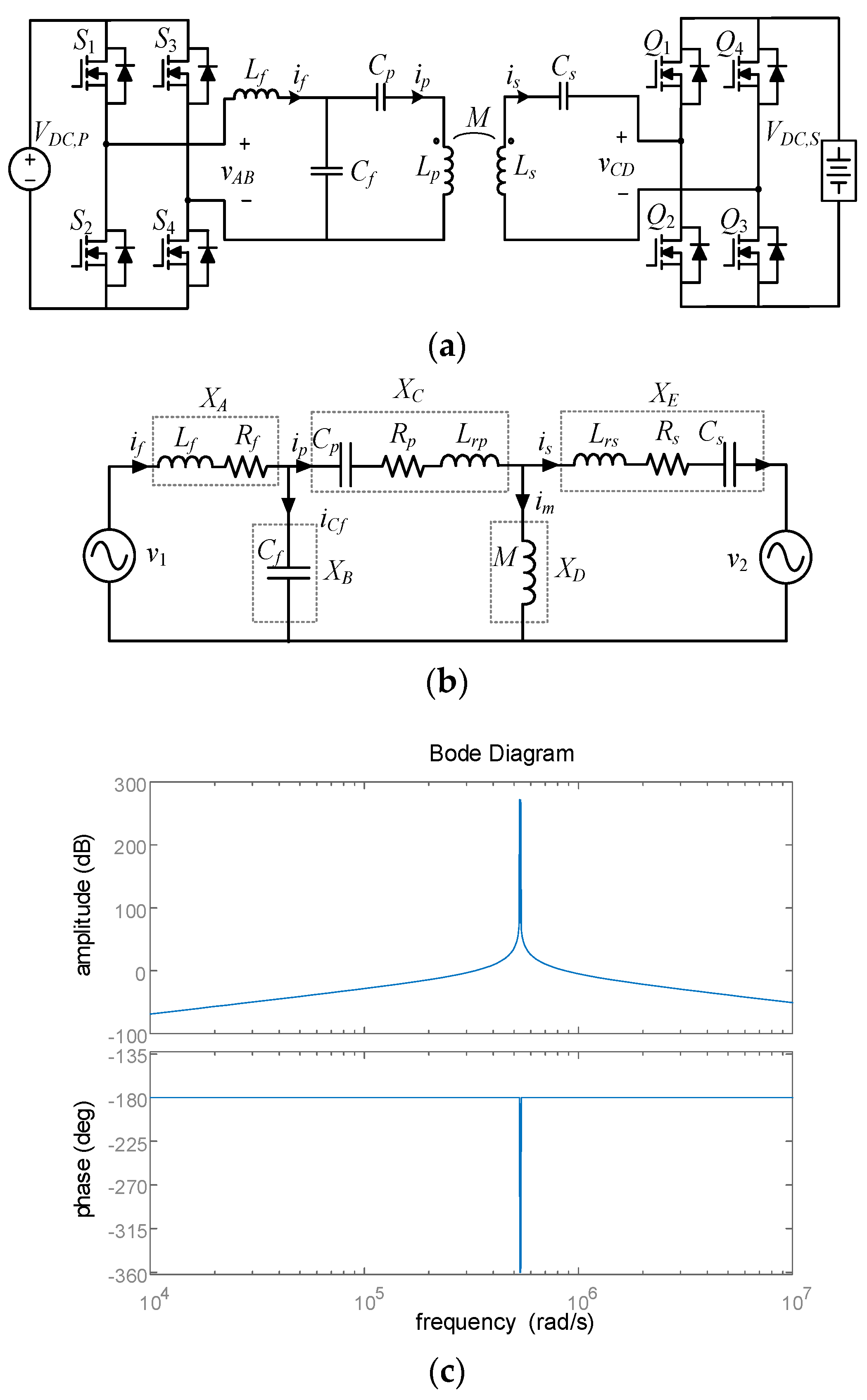
2.1. Proposed System and Its Mathematical Model

The schematic of the proposed DAB-based LCC-S compensated BDWPT system is shown in Figure 2a. On the primary side, a full-bridge converter H1 is formed by switches S1~S4, which supplies an AC voltage to the compensation network from the DC-link voltage VDC,P. VDC,P is the DC voltage source, which represents the output voltage of the PFC rectifier connected to the grid [14,22] or the battery energy storage system (BESS) [24,25]. The secondary-side full-bridge converter H2 is formed by switches Q1~Q4. These two H-bridges consist of a traditional DAB structure. The output voltage of H2 is shown as VDC,S, which normally represents an Evs battery. An LCC network consisting of Cp, Cf and Lf is placed on the primary side. Cs is the resonant capacitor at the secondary side. Two coils, Lp and Ls, are coupled through mutual inductance (M) and form a loosely coupled transformer. The coupling coefficient k is defined as k = M / L P L S . The parasitic resistance of the two coils is Rp and Rs, respectively. Rf is the parasitic resistance of Lf. vAB and vCD are the output voltage chopped by full-bridges H1 and H2. ip, is, if are the current flowing through the Lp, Ls and Lf, respectively. The LCC-S compensation structure is designed as a CV network. Lf resonant with Cf, Ls resonant with Cs, Lp resonant with Cf and Cp. The control scheme of the proposed converter switches and relevant waveforms are illustrated in Figure 2d. The parameter configuration follows the rules published in [5,12,13].
ω 0 = 2 π f 0 = 1 L s C s = 1 L f C f
1 ω 0 C p + 1 ω 0 C f = ω 0 L p
Because the network of Cf, Lf, Cp and Lp has filter characteristics, the harmonic component of the output current is small. The bode plot of the Cf, Lf, Cp and Lp networks is shown in Figure 2c; they have a good capability to suppress high- and low-frequency harmonics. The center frequency is the fundamental harmonic, while the other high-frequency and low-frequency harmonics are significantly suppressed. The power calculation is performed using the fundamental harmonic approximation (FHA) method to simplify the analysis. The FHA method is applied to analyze the power transfer ability of the proposed BDWPT system. A T-type equivalent circuit is depicted in Figure 2b, where Lrp and Lrs are the leakage inductance of two coils, respectively. v1 and v2 are the fundamental component of vAB and vCD, respectively, which can be derived by Fourier series:
v 1 = V 1 0 = 2 2 π V D C , P sin α 2 0
v 2 = V 2 θ = 2 2 π V D C , S sin β 2 θ .
where α and β are the phase-shift angles of two H-bridges. θ is the relative phase angle between v1 and v2. V1 and V2 are the magnitudes of v1 and v2. The power transfer of the proposed control system has thus been controlled by v1 and v2.
According to Kirchhoff’s laws, the circuit can be represented by the following equation:
v 1 0 v 2 0 0 = X A X B 0 0 0 0 - X B   X C X D 0 0 0 0 - X D X E 1 1 1 0 0 0 0 1 1 1   i f i C f i p i m i s
where XA~XE represents the equivalent impedance of each branch, X A = j ω L f + R f , X B = 1 / j ω C f , X C = j ω L r p + 1 / j ω C p + R p , X D = j ω M , X E = j ω L s + 1 / j ω C s + R s . By solving the Equation (5), current flows through each branch can be calculated as follows:
  i f i p i s i C f i m = 1 X 0 v 1 ( X B X D + X B X E + X C X D + X C X E + X D X E ) v 2 X B X D v 1 ( X B X D + X B X E ) v 2 ( X A X D + X B X D ) v 1 X B X D v 2 ( X A X B + X A X C + X A X D + X B X C + X B X D ) v 1 ( X C X D + X C X E + X D X E ) + v 2 X A X D v 1 X B X E + v 2 ( X A X B + X A X C + X B X C )
X 0 = X A X B X D + X A X B X E + X A X C X D + X A X C X E         + X B X C X D + X B X C X E + X A X D X E + X B X D X E
When considering the parasitic resistance of the inductor,
X A + X B = 1 j ω C P + j ω L r P + j ω M + R P R P
X D + X E = 1 j ω C f + j ω L f + R f R f
where Rp and Rf are the parasitic resistances of XA and XE branches, respectively. In each branch, the parasitic resistance is much less than the total impedance value of the corresponding branch. Therefore, the quadratic terms of X A + X B and X D + X E is neglected in Equation (6).
With the parameter configuration rules according to Equations (1) and (2), input current if can be represented by
i f = X D ( v 1 X E v 2 X B ) + v 1 ( X B + X C ) R f X C R p R f + X A X B R f + X D X E R s
Coil resistances Rp and Rs are much smaller than other impedances. To simplify the expression of Equation (7), the higher-order terms of Rp and Rs in the numerator and denominator are ignored, and if can be expressed as
i f = L f M R f M 2 + R s L f 2 ( v 1 M L f v 2 ) .
With a similar simplification method, current flows through two coils, Lp and Ls, can be calculated and simplified as
i p = j ( v 1 L f R f + v 2 M R p ) ω 0 ( R f L f 2 + R p M 2 )
i s = L f 2 R f M 2 + R s L f 2 ( v 1 M L f v 2 ) .
Thus, the expressions for the active power P1 and P2 and the reactive power Q1 and Q2 on the primary and secondary sides of the BDWPT system can be obtained:
P 1 = Re v 1 i f = 1 2 L f M V 1 R f M 2 + R s L f 2 ( V 1 M L f cos θ V 2 ) .
Q 1 = Im v 1 i f = 1 2 L f M V 1 V 2 sin θ R f M 2 + R s L f 2 .
P 2 = Re v 2 i s = 1 2 L f 2 V 2 R f M 2 + R s L f 2 ( V 1 M L f V 2 cos θ )
Q 2 = Im v 2 i s = 1 2 L f M V 1 V 2 sin θ R f M 2 + R s L f 2 .
Through the control of S1S4 and Q1Q4, the voltage v1 and v2 of the system can be changed, and the transmission power of the system can be changed.

2.2. Power Transmission Characteristics

From Equations (12) and (14), reactive power equals zero when θ is 0° or 180°. Apparently, transfer active power is positive when θ = 180°, which means the directional of power flow is fixed. Therefore, θ = 0° is applied to realize bidirectional power transfer. The direction of power flow is determined by the relative magnitude between V 1 M / L f and V2. When V 1 M / L f > V 2 , power flows from the primary side to the secondary side. When V 1 M / L f < V 2 , power flows from the secondary side to the primary side. Additionally, the amount of power flow is positively related to the difference between V2 and V 1 M / L f . The power transmission of the system can be changed by changing the difference in voltage V 1 M / L f and V2.
The relative phase angle θ is essentially maintained constant at 0°, and therefore, the system operates at unity power factor. When θ is 0°, both the amount and direction of power flow can be regulated by controlling V1 and V2, which are determined by DC-bus voltages (VDC,P and VDC,S) and phase shift angles (α and β), as shown in Equations (3) and (4). When θ is 0°, a diagram depicts the phasor relationship between the variables of the FHA equivalent circuit of the proposed system, as shown in Figure 3.
The relationship between primary DC-bus voltage VDC,P and transfer power of the proposed LCC-S system and typical CC-BDWPT systems is illustrated in Figure 4. The secondary DC-bus voltage VDC,S is kept at 100 V to show the power transmission capability of the different circuits in a more direct way. The component parameters of the LCC-S circuit are shown in Table 1. The CC-BDWPT models published in [14,16,18] are applied to calculate the relationship between system transmission power and DC-bus voltage. Mathematical expressions of the maximum transfer power of CC-BDWPT systems are listed in Table 2. As illustrated by Figure 4, the power transmission capacity of the CC-BDWPT systems changes little with the bus voltage. Therefore, when the transmission power is away from the maximum power of the system, the DC-bus voltage needs to be adjusted in a large range. This means that the phase shift angle will change dramatically with PSM, which makes it hard to maintain low switching loss and low reactive power at the same time. Additionally, the proposed DAB-based LCC-S system is capable of operating over a wider range of transfer power with limited variation in VDC,P. Although the sensitivity to VDC,P enhances the transfer power regulation capability of the proposed system, it creates challenges in precisely controlling the full-bridge output voltages when the resistance of the coils is too small. In summary, WPT systems with CV compensation networks represented by LCC-S have higher power transmission capability than CC-BDWPT systems.
The WPT system is very similar to other isolated power electronic topologies. The only difference is that the transformers wound by magnetic core are replaced by two coils that are coupled with each other through air. In order to eliminate the impact of the inductance in traditional isolated DC-DC converters, the resonance concept of active components has already been widely studied, analyzed and applied [26,27,28]. For traditional isolated DC-DC converters, the magnetic core provides a sufficient coupling coefficient for the primary and secondary side coils, so the self-induction of the primary and secondary side coils does not need to be large enough to obtain the desired mutual inductance value. Traditional LLC converter [26] can be seen as a CV output circuit when the resonant capacitor Cr is resonant with primary-side inductance Lr1. The AC equivalent circuit of a traditional LLC converter is shown in Figure 5, where the mutual inductance M is much larger than the secondary-side leakage inductance Lr2. The transfer power of the LLC converter can be approximately expressed as
S L L C = v 2 ( v 1 v 2 ) j w L r 2 + R 2 .
Due to the low resistance value provided by the transformer, the transfer power can be theoretically close to infinity when the AC equivalent voltage of two sides in the model is at an unbalanced state. Thus, it is difficult to precisely control the transmission power by controlling the difference between the primary and secondary voltages. While WPT is a type of isolated DC-DC converter with unavoidable coil resistance, the resistance of a few hundred milliohms makes the method of controlling the voltage difference to adjust the transmission power realistic.

3. Performance Comparison with CC-BDWPT Systems

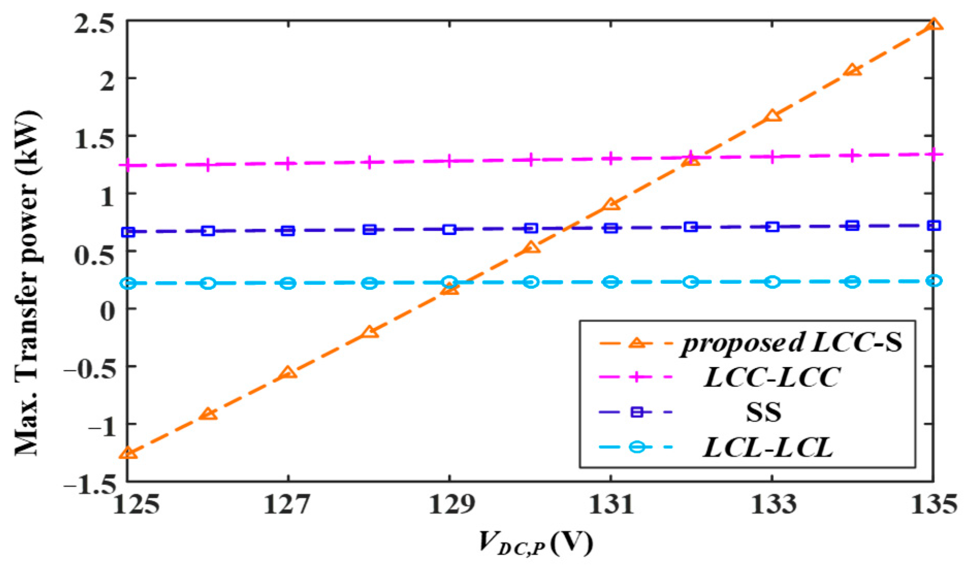
3.1. Better Regulation Capability of Transfer Power

Mathematical expressions of the transfer power of CC-BDWPT systems are listed in Table 2. The relationship between primary side DC-bus voltage VDC,P and maximum active power of different topologies under unit power factor conditions has been illustrated in Figure 4. The parameters of resonant components in CC-BDWPT systems are the same as that in [4,6,8]. It can be found that the maximum transfer power of CC-BDWPT systems is not sensitive to the VDC,P and stays almost constant when primary DC-bus voltage varies. But, the transfer power of the proposed LCC-S can be modulated by changing the difference between V 1 M cos θ / L f and V2, which strengthens the power regulation capacity of the system. As illustrated by Figure 4, the proposed LCC-S system is capable of operating over a wider range of transfer power with the variation in VDC,P. Additionally, the proposed LCC-S has extra control freedom of power regulation in both directions, which means that both the amount and the direction of the transfer power can be controlled by simply changing either side of the full-bridge output voltage.
Moreover, from the expressions in Table 2, for the SS-compensated BDWPT, since the mutual inductance M is in the denominator position of the transmitted power expression, high transmission power can be obtained by a small mutual inductance M design. The misalignment of the coils will sharply increase the transmission power of the system, which brings difficulties to stable power control. The LCL-LCL compensated BDWPT system has a limited power transfer capability. For high power transferring conditions, LCL-LCL topology should have a high value of M and a small value of Lp and Ls, which is difficult in practical design.
The operating waveforms of the PSM method under unit power factor conditions are presented in Figure 6. φ is the phase-shift angle of the primary-side voltage. The operation of PSM in one period can be divided into four modes:
Mode 1 [t0–t1]: At t0, switch S4 turns on. During this mode, the current if flows in the positive direction, VDC,P supplies the power, and current if flows through S1 and S4.
Mode 2 [t1–t2]: During this interval, switch S1 is OFF, S2 is ON. Current if flows through S2 and S4.
Mode 3 [t2–t3]: At t2, switch S3 turns on. During this mode, the current if flows in the negative direction, VDC,P supplies the power, and current if flows through S2 and S3.
Mode 4 [t3–t4]: During this interval, switch S1 is OFF, S2 is ON. Current if flows through S1 and S3.
During the period when the full-bridge output voltages are 0 V, current freewheels are outputted via the switches when the power source is in open-load condition and does not supply the energy to the system. However, due to the constant power losses caused by the freewheeling current via the switch, the losses are higher at a fixed transmitted power.
As analyzed before, SS and LCL-LCL topology is not suitable for high-transfer power situations. Although LCC-LCC topology can provide high transmission power, larger phase-shift angles are essential at the same time when the system operates under light load. From Figure 7, when the transfer power changes from full-load (1100 W) to half-load (550 W), the phase-shift angle changes from 180° to 60°.
Compared with CC-BDWPT systems, LCC-S topology can be easily applied for high-power applications at a wide range of loads with larger phase-shift angles. From Figure 7, when the transfer power changes from full-load to half-load, the phase-shift angle changes from 180° to 162°; thus, the current freewheeling time through the switches is largely reduced.

3.2. Reduced Switching Losses with PSM

The drain-to-source voltage Vds and current Ids transitions overlap over finite time and result in switching losses. The overlap areas of Vds and Ids can be estimated by using the area of a triangle, which can be expressed as:
P S W = 2 t o n + t o f f   i f ( t 1 ) V D C , P  
where ton and toff are the overlapping times of Vds and Ids during turn-on transition and turn-off transition, respectively. i f ( t 1 ) is calculated by the transfer power and phase-shift angle:
i f ( t 1 ) = π P 2 V D C , P   cos ( α 2 ) .
The variation in switching loss PSW and phase-shift angle α with transfer power P is shown in Figure 8. As illustrated by Figure 8, the LCC-S system has much lower switching losses than CC-BDWPT systems over a full range of loads. The LCC-S system is capable of operating over a wide range of power with a smaller phase shift range. In CC-BDWPT systems, α changes within a large range, and switching losses are much larger when the system is not operating at the rated output power.

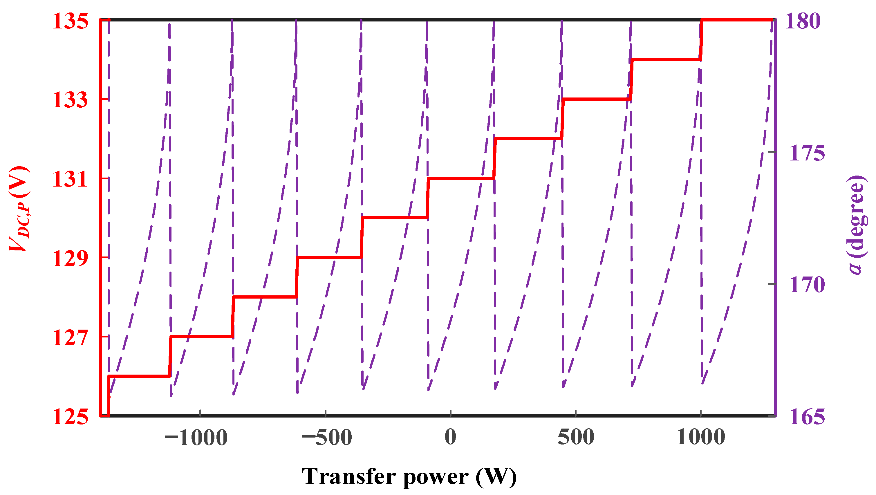
4. Hybrid Control Strategy for Proposed System

As discussed before, the LCC-S compensated BDWPT system can work in higher power situations with stronger power regulation capabilities than CC-BDWPT systems. Additionally, high transfer power output control can be achieved with a small variation in phase-shift angle. However, the superior performance depends on matching the full bridge output voltage of the primary and secondary sides. The difference between the voltage V 1 M / L f and V2 is desired to be controlled on a relatively small scale. Normally, a cascaded DC/DC converter can be applied to regulate the DC voltage source. However, the transfer power is really sensitive to the magnitude of the voltage source of the LCC-S compensated BDWPT system compared with the CC-BDWPT system or other resonant circuits. Therefore, a hybrid control method combining DC voltage control and PSM control is applied. Primary DC-bus voltage VDC,P changes in a relatively large step each time. PSM is applied under different VDC,P to control the transfer power in accuracy.
In general, ZVS conditions will be lost when PSM is employed. However, the LCC network can contribute high-order harmonic currents, and ZVS can still be realized within a small phase shift range. The proposed hybrid controlling strategy is also able to realize ZVS at a full range of loads while maintaining accurate transfer power control at the same time. The variation in VDC,P and phase-shift angle α under different transfer power is shown in Figure 5; VDC,P changes 1 V each time, and α changes within 15°.

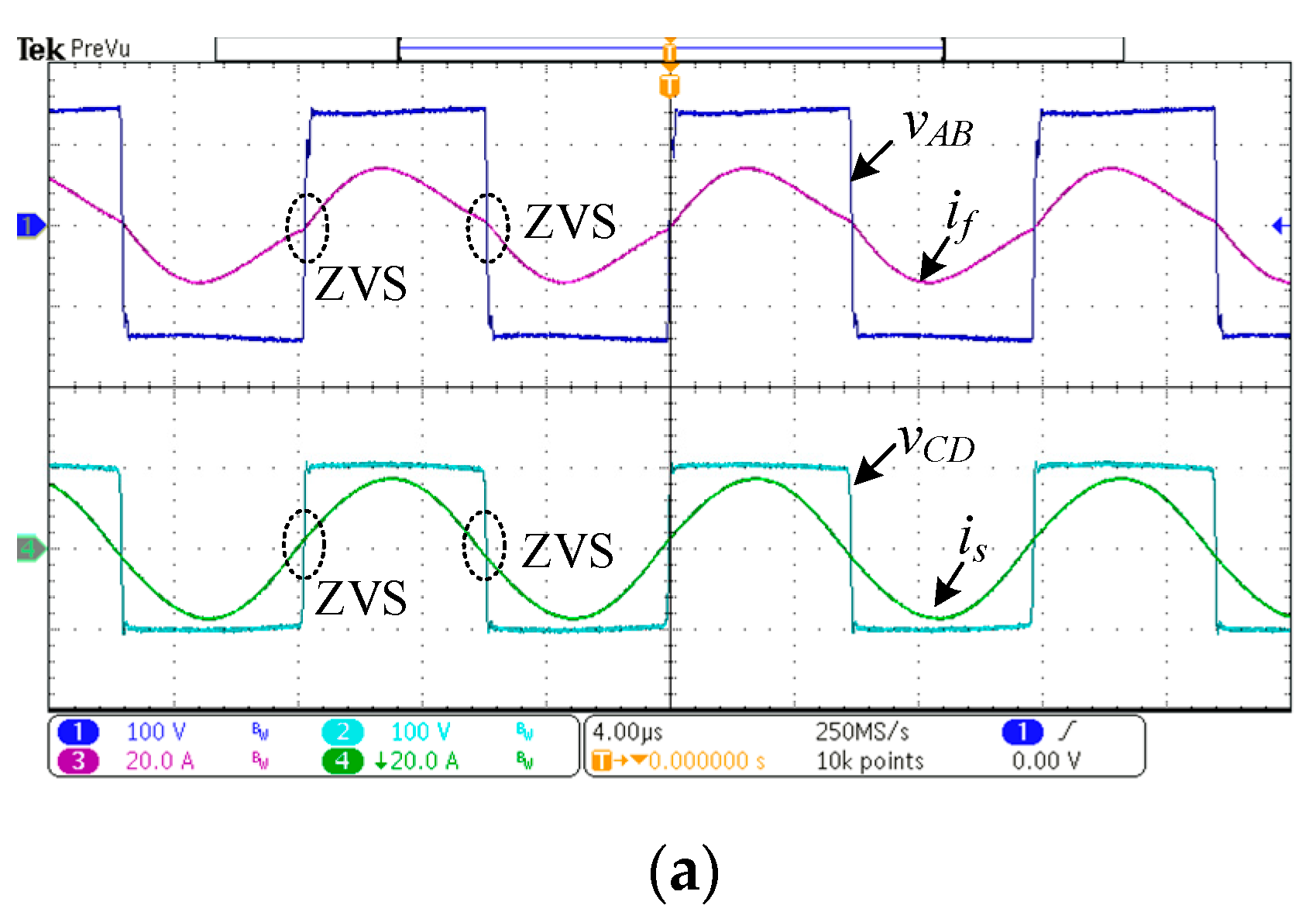
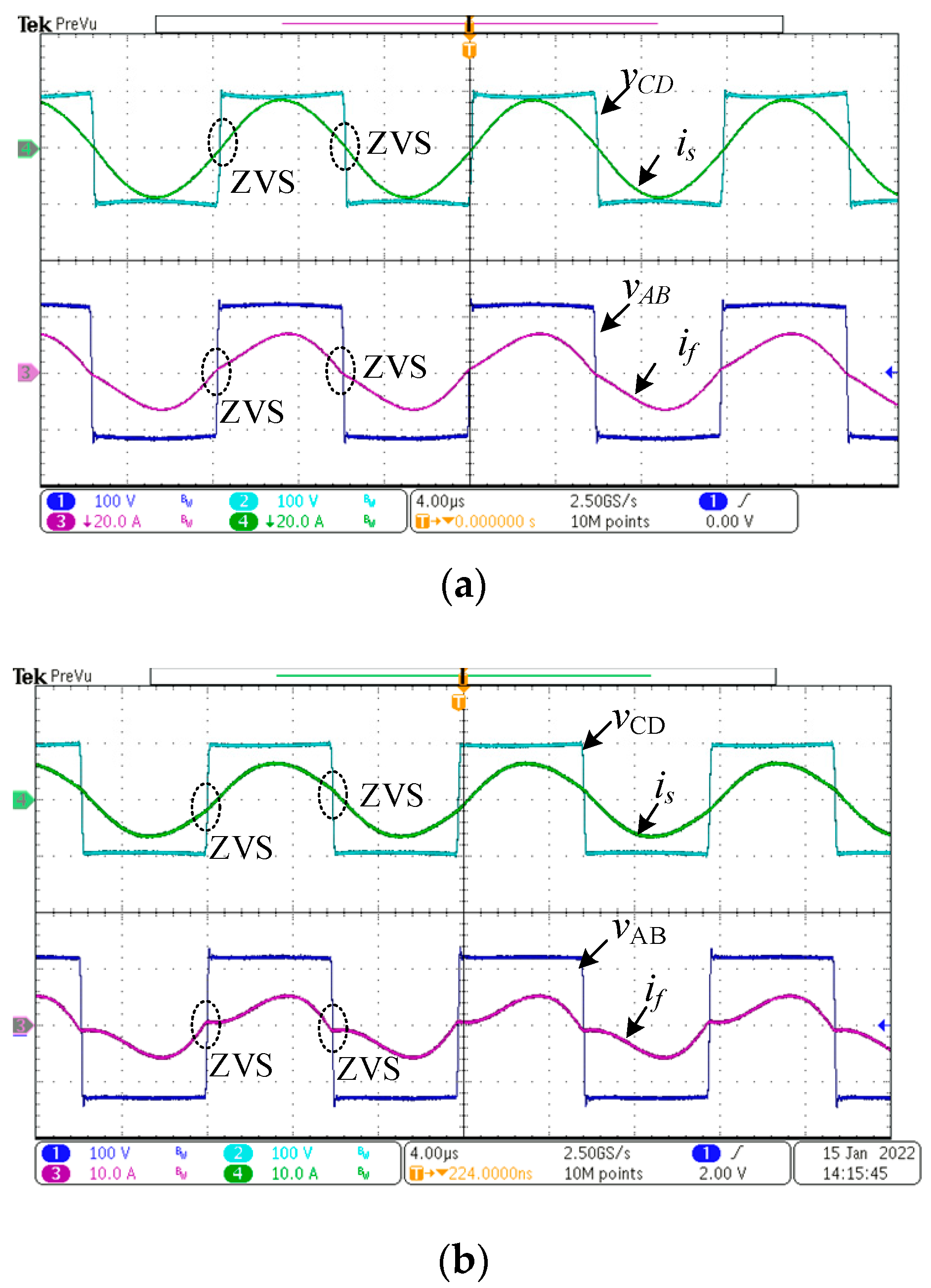
5. Experimental Verification

To verify the characteristics of the proposed LCC-S compensated BDWPT system, a hardware prototype is built, as shown in Figure 9. Two simple circular pads are employed as the magnetic coupler. The inner and outer diameters of the pads are 241 mm and 332 mm, respectively, and the distance between the two pads is 105 mm. The distance between the inductances of the primary side and the secondary side in this experiment is about 112 mm. The coupling coefficient of the system is about 0.24. The detailed parameters measured by the LCR meter have been provided in Table 1.
The switching frequency is fixed at 85 kHz. The secondary DC-bus voltage is 100 V. The parameters of hardware components are listed in Table 2, where M/Lf is about 0.767. In this experiment, θ is controlled to be zero in order to achieve a unity power factor. Figure 10 shows the experimental waveforms of output voltages and currents of H-bridges when power flows from the primary side to the secondary side. Figure 11 shows the experimental waveforms when power flows from the secondary side to the primary side. For the waveforms in Figure 10a,b and Figure 11a,b, the power transfer is controlled by DC-bus voltage regulation ( V 1 M / L f V 2 ), while for the waveforms in Figure 10c and Figure 11c, the PSM is employed.
In Figure 10a, VDC,P is 142 V, and V 1 M / L f V 2 = 11.4   V . The transfer power is 1.079 kW. When VDC,P is reduced to 138 V, V 1 M / L f V 2 = 7.4   V . The transfer power dropped to 570.5 W, and the experimental waveforms are shown in Figure 10b. Compared with Figure 10a, the primary-side phase shift angle α is set to be 148.0° in Figure 10c, and the transfer power drops to 577.6 W. The phase-shift angle α changes by only 32.0°, which is much smaller than that in CC-BDWPT systems. Additionally, ZVS can still be realized within a small phase shift range.
In Figure 11a, VDC,P is 120 V, V 1 M / L f V 2 = 10.3   V . The transfer power is 1.108 kW. When VDC,P is increased to 125 V, V 1 M / L f V 2 = 5.2   V . The transfer power dropped to 489.3 W, and the experimental waveforms are shown in Figure 11b. Compared with Figure 11b, the primary-side phase shift angle α is set to be 149.8° in Figure 11c. The transfer power increases to 800.3 W, and α changes by only 30.2°. In Figure 11c, Q2 and Q4 cannot realize ZVS. Under this condition, the high-frequency harmonic current of is is not large enough to achieve ZVS. But the switching losses are quite low due to if (t2) is only about 1.8 A.
The above experimental results clearly demonstrated that the amount of transfer power of the proposed LCC-S can be controlled by modulating primary DC-bus voltage VDC,P or primary phase-shift angle α to control the amount of transfer power, respectively. A wide range of soft-switching can also be achieved.

6. Conclusions and Discussion

A CV-BDWPT system (LCC-S) to realize the two-way wireless power transfer has been proposed. A mathematical model has been presented to show that the reactive power can be controlled to be zero when the output voltages of H-bridges are in the same phase, and the direction and amount of power flow can be controlled by changing the difference between V 1 M / L f and V2. This topology can also be applied as a UDWPT system, which has the advantages of higher maximum transfer power and reduced switching losses. The advantage of the proposed design is that the system can transfer power that is not limited by the inductance of primary side and secondary side coils and their mutual inductance. In our system, the transfer power is sensitive to the output voltages of either side of H-bridges, so significant changes in the transmission of energy can be obtained by relatively small changes in phase-shift angles. While each coin has two sides, the disadvantage of the proposal is that the system is sensitive to the variation in DC-bus voltage. A 1.1 kW experiment is established to verify that a small change in phase-shift angle or DC-bus voltage can largely change the transfer power of the system while realizing the unit power factor at the same time.

Author Contributions

Conceptualization, G.L.; methodology, G.L.; software, Z.C.; validation, G.L. and Z.C.; formal analysis, C.F. and Z.S.; investigation, G.L.; writing—original draft preparation, G.L.; writing—review and editing, C.F. and Z.S.; visualization, Z.C.; supervision, X.P.; project administration, X.P.; funding acquisition, X.P. All authors have read and agreed to the published version of the manuscript.

Funding

This research was funded by the Shenzhen Science and Technology Plan Project under Grant GJHZ20220913143008016.

Data Availability Statement

All data included in this study are available upon request by contact with the corresponding author.

Conflicts of Interest

The authors declare no conflicts of interest.

References

  1. Liu, C.; Gu, C.; Li, C. Non-contact hand interaction with smart phones using the wireless power transfer features. In Proceedings of the IEEE Radio and Wireless Symposium (RWS), San Diego, CA, USA, 25–28 January 2015; pp. 20–22. [Google Scholar]
  2. Wu, C.; Kim, H.; Penugonda, S.; Fan, J. Analysis and Modeling of the Common-Mode Conducted EMI From a Wireless Power Transfer System for Mobile Applications. IEEE Trans. Electromagn. Compat. 2021, 63, 2143–2150. [Google Scholar] [CrossRef]
  3. Chen, Q.; Wong, S.C.; Tse, C.K.; Ruan, X. Analysis, Design, and Control of a Transcutaneous Power Regulator for Artificial Hearts. IEEE Trans. Biomed. Circuits Syst. 2009, 3, 23–31. [Google Scholar] [CrossRef] [PubMed]
  4. Pucci, N.; Kwan, C.H.; Yates, D.C.; Arnold, A.D.; Keene, D.; Whinnett, Z.I.; Mitcheson, P.D. Effect of Fields Generated through Wireless Power Transfer on Implantable Biomedical Devices. In Proceedings of the 2019 IEEE PELS Workshop on Emerging Technologies: Wireless Power Transfer (WoW), London, UK, 18–21 June 2019; pp. 160–164. [Google Scholar]
  5. Cheng, Z.; Lei, Y.; Song, K.; Zhu, C. Design and Loss Analysis of Loosely Coupled Transformer for an Underwater High-Power Inductive Power Transfer System. IEEE Trans. Magn. 2015, 51, 1–10. [Google Scholar]
  6. Lopes, I.F.; Lacerda Valle, R.; Azevedo Fogli, G.; Ferreira, A.A.; Gomes Barbosa, P. Low-Frequency Underwater Wireless Power Transfer: Maximum Efficiency Tracking Strategy. IEEE Lat. Am. Trans. 2020, 18, 1200–1208. [Google Scholar] [CrossRef]
  7. Huang, Z.; Wong, S.; Tse, C.K. Design of a Single-Stage Inductive-Power-Transfer Converter for Efficient EV Battery Charging. IEEE Trans. Veh. Technol. 2017, 66, 5808–5821. [Google Scholar] [CrossRef]
  8. Vu, V.-B.; Tran, D.-H.; Choi, W. Implementation of the Constant Current and Constant Voltage Charge of Inductive Power Transfer Systems with the Double-Sided LCC Compensation Topology for Electric Vehicle Battery Charge Applications. IEEE Trans. Power Electron. 2017, 33, 7398–7410. [Google Scholar] [CrossRef]
  9. Lu, J.; Zhu, G.; Wang, H.; Lu, F.; Jiang, J.; Mi, C.C. Sensitivity Analysis of Inductive Power Transfer Systems with Voltage-Fed Compensation Topologies. IEEE Trans. Veh. Technol. 2019, 68, 4502–4513. [Google Scholar] [CrossRef]
  10. Chen, Y.; Zhang, H.; Park, S.-J.; Kim, D.-H. A Switching Hybrid LCC-S Compensation Topology for Constant Current/Voltage EV Wireless Charging. IEEE Access 2019, 7, 133924–133935. [Google Scholar] [CrossRef]
  11. Lu, J.; Zhu, G.; Lin, D.; Zhang, Y.; Wang, H.; Mi, C.C. Realizing Constant Current and Constant Voltage Outputs and Input Zero Phase Angle of Wireless Power Transfer Systems with Minimum Component Counts. IEEE Trans. Intell. Transp. Syst. 2021, 22, 600–610. [Google Scholar] [CrossRef]
  12. Niu, H.; Li, G.; Lu, J.; Pan, X. Parameter Identification Method with Dynamic Impedance Modulation for the DWPT System. IEEE J. Emerg. Sel. Top. Power Electron. 2022, 10, 6332–6344. [Google Scholar] [CrossRef]
  13. Jou, H.-L.; Wu, J.-C.; Wu, K.-D.; Kuo, C.-Y. Bidirectional DC–DC Wireless Power Transfer Based on LCC-C Resonant Compensation. IEEE Trans. Power Electron. 2021, 36, 2310–2319. [Google Scholar] [CrossRef]
  14. Mohammad, M.; Onar, O.C.; Su, G.J.; Pries, J.; Galigekere, V.P.; Anwar, S.; Asa, E.; Wilkins, J.; Wiles, R.; White, C.P.; et al. Bidirectional LCC–LCC-Compensated 20-kW Wireless Power Transfer System for Medium-Duty Vehicle Charging. IEEE Trans. Transp. Electrif. 2021, 7, 1205–1218. [Google Scholar] [CrossRef]
  15. Liu, Y.; Madawala, U.K.; Mai, R.; He, Z. Zero-Phase-Angle Controlled Bidirectional Wireless EV Charging Systems for Large Coil Misalignments. IEEE Trans. Power Electron. 2020, 35, 5343–5353. [Google Scholar] [CrossRef]
  16. Jiang, Y.; Wang, L.; Fang, J.; Zhao, C.; Wang, K.; Wang, Y. A Joint Control with Variable ZVS Angles for Dynamic Efficiency Optimization in Wireless Power Transfer System. IEEE Trans. Power Electron. 2020, 35, 11064–11081. [Google Scholar] [CrossRef]
  17. Madawala, U.K.; Thrimawithana, D.J. A Bidirectional Inductive Power Interface for Electric Vehicles in V2G Systems. IEEE Trans. Ind. Electron. 2011, 58, 4789–4796. [Google Scholar] [CrossRef]
  18. Tang, Y.; Chen, Y.; Madawala, U.K.; Thrimawithana, D.J.; Ma, H. A New Controller for Bidirectional Wireless Power Transfer Systems. IEEE Trans. Power Electron. 2018, 33, 9076–9087. [Google Scholar] [CrossRef]
  19. Zhang, X.; Cai, T.; Duan, S.; Feng, H.; Hu, H.; Niu, J.; Chen, C. A Control Strategy for Efficiency Optimization and Wide ZVS Operation Range in Bidirectional Inductive Power Transfer System. IEEE Trans. Ind. Electron. 2019, 66, 5958–5969. [Google Scholar] [CrossRef]
  20. Yenil, V.; Cetin, S. Load Independent Constant Current and Constant Voltage Control of LCC-Series Compensated Wireless EV Charger. IEEE Trans. Power Electron. 2022, 37, 8701–8712. [Google Scholar] [CrossRef]
  21. Li, M.; Deng, J.; Chen, D.; Wang, W.; Wang, Z.; Li, Y. A Control Strategy for ZVS Realization in LCC-S Compensated WPT System with Semi Bridgeless Active Rectifier for Wireless EV Charging. In Proceedings of the 2021 IEEE Energy Conversion Congress and Exposition (ECCE), Vancouver, CA, USA, 10–14 October 2021; pp. 5823–5827. [Google Scholar]
  22. Ann, S.; Lee, B.K. Analysis of Impedance Tuning Control and Synchronous Switching Technique for a Semibridgeless Active Rectifier in Inductive Power Transfer Systems for Electric Vehicles. IEEE Trans. Power Electron. 2021, 36, 8786–8798. [Google Scholar] [CrossRef]
  23. Ann; Son, W.-J.; Byun, J.; Lee, J.H.; Lee, B.K. Switch Design for a High-Speed Switching Semi—Bridgeless Active Rectifier of Inductive Power Transfer Systems Considering Reverse Recovery Phenomenon. In Proceedings of the 2019 10th International Conference on Power Electronics and ECCE Asia (ICPE 2019—ECCE Asia), Busan Exhibition & Convention Center, Busan, Republic of Korea, 27–30 May 2019; pp. 1–6. [Google Scholar]
  24. Lawder, M.T.; Suthar, B.; Northrop, P.W.; De, S.; Hoff, C.M.; Leitermann, O.; Crow, M.L.; Santhanagopalan, S.; Subramanian, V.R. Battery Energy Storage System (BESS) and Battery Management System (BMS) for Grid-Scale Applications. Proc. IEEE 2014, 102, 1014–1030. [Google Scholar] [CrossRef]
  25. Argiolas; Stecca, M.; Ramirez-Elizondo, L.M.; Soeiro, T.B.; Bauer, P. Optimal Battery Energy Storage Dispatch in Energy and Frequency Regulation Markets While Peak Shaving an EV Fast Charging Station. IEEE Open Access J. Power Energy 2022, 9, 374–385. [Google Scholar] [CrossRef]
  26. Yang, B.; Lee, F.C.; Zhang, A.J.; Huang, G. LLC resonant converter for front end DC/DC conversion. In Proceedings of the APEC. Seventeenth Annual IEEE Applied Power Electronics Conference and Exposition (Cat. No. 02CH37335), Dallas, TX, USA, 10–14 March 2002; pp. 1108–1112. [Google Scholar]
  27. Jung, J.-H.; Kim, H.-S.; Ryu, M.-H.; Baek, J.-W. Design Methodology of Bidirectional CLLC Resonant Converter for High-Frequency Isolation of DC Distribution Systems. IEEE Trans. Power Electron. 2013, 28, 1741–1755. [Google Scholar] [CrossRef]
  28. Zuo, Y.; Pan, X.; Wang, C. A Reconfigurable Bidirectional Isolated LLC Resonant Converter for Ultra-Wide Voltage-Gain Range Applications. IEEE Trans. Ind. Electron. 2022, 69, 5713–5723. [Google Scholar] [CrossRef]
Figure 1. (a) Basic structure of UDWPT system. (b) Basic structure of DAB-based BDWPT system.
Energies 17 04519 g001
Figure 2. (a) BDWPT system with LCC-S compensation. (b) T-type equivalent circuit with FHA method. (c) The bode plot of the Cf, Lf, Cp and Lp networks. (d) the control scheme of switches and output voltage waveform.
Energies 17 04519 g002aEnergies 17 04519 g002b
Figure 3. (a) Primary side delivers power. (b) Primary side receives power.
Energies 17 04519 g003
Figure 4. The relationship between primary DC-bus voltage VDC,P and maximum active power of different topologies with fixed M (28.0 μH) and secondary DC-bus voltage VDC,S (100 V) under unit power factor condition [14,16,18].
Energies 17 04519 g004
Figure 5. T-type equivalent circuit of traditional LLC converter.
Energies 17 04519 g005
Figure 6. Typical waveforms of full-bridge converter in WPT system under unit power factor condition.
Energies 17 04519 g006
Figure 7. The variation in switching losses PSW and phase shift angle α with transfer power P when VDC,P and VDC,S are fixed at 128 V and 100 V.
Energies 17 04519 g007
Figure 8. Variation in primary DC-bus voltage VDC,P and phase-shift angle α under different transfer power with proposed hybrid control strategy.
Energies 17 04519 g008
Figure 9. Experimental prototype: (a) H-bridges and LCC-S compensation structure. (b) Magnetic coupler.
Energies 17 04519 g009
Figure 10. Operating waveforms of output voltages and currents of H-bridges when power flows from the primary side to the secondary side: (a) VDC,P = 142 V; VDC,S = 100 V. (b) VDC,P = 138 V; VDC,S = 100 V. (c) VDC,P = 142 V; VDC,S = 100 V; α = 148.0°.
Energies 17 04519 g010aEnergies 17 04519 g010b
Figure 11. Operating waveforms of output voltages and currents of H-bridges when power flows from the secondary side to the primary side: (a) VDC,P = 120 V; VDC,S = 100 V. (b) VDC,P = 125 V; VDC,S = 100 V. (c) VDC,P = 125 V; VDC,S = 100 V; α = 148.0°.
Energies 17 04519 g011aEnergies 17 04519 g011b
Table 1. System parameters.
SymbolParametersValues
Lpprimary-side coil inductance121.34 μH
Lssecondary-side coil inductance121.56 μH
Lfcompensation inductance36.175 μH
Mmutual inductance29.0 μH
kcoupling coefficient0.24
Cpseries compensation capacitor29.34 nF
Csseries compensation capacitor41.71 nF
Cfcompensation capacitor95.94 nF
Rpparasitic resistance of Cp0.179 Ω
Rfparasitic resistance of Cf0.049 Ω
Rsparasitic resistance of Cs0.182 Ω
Table 2. Transfer power comparison of DAB-based CC-BDWPT systems and proposed LCC-S compensated BDWPT system.
StructuresMathematical Expression
of Transfer Power
Max Powerin Theory
SS V 1 V 2 ω 0 M sin α 2 sin β 2 V 1 V 2 ω 0 M
LCL-LCL V 1 V 2 M ω 0 L p L S sin α 2 sin β 2 V 1 V 2 M ω 0 L p L S
LCC-LCC V 1 V 2 M ω 0 L f 2 sin α 2 sin β 2 V 1 V 2 M ω 0 L f 2
proposed
S-LCC
L f 2 V 1 ( V 1 V 2 M cos θ / L f ) R f M 2 + R p L f 2 L f 2 V 1 2 R f M 2 + R p L f 2
Disclaimer/Publisher’s Note: The statements, opinions and data contained in all publications are solely those of the individual author(s) and contributor(s) and not of MDPI and/or the editor(s). MDPI and/or the editor(s) disclaim responsibility for any injury to people or property resulting from any ideas, methods, instructions or products referred to in the content.

