Abstract
Incorporating AC-type flying capacitors (FC) between series-connected devices is an effective way to enhance the rated voltage for high-power applications based on current source converters (CSCs). Through appropriate modulation and FC voltage control, it is possible to achieve improved DC bus voltage quality with reduced common-mode voltage (CMV) and low dv/dt. On the other hand, the parallel CSC is a popular choice for increasing the system’s rated current to accommodate higher power applications. The use of interleaved modulation techniques can improve the harmonic performance of parallel converters while reducing the need for passive filters. The modular flying capacitor clamped (FCC)-CSC structure can combine these advantages, achieving higher rated power along with improved power quality on both the DC and AC sides. Moreover, the enhanced AC quality contributes to the regulation of FC voltage and further improves the DC-side voltage quality. This paper analyzes the operation principle of the parallel FCC-CSC structure and proposes an interleaved space vector modulation (SVM) method to enhance the harmonic performance of the AC output. Additionally, an optimized zero-state replacement (ZSR) based FC voltage control and a DC-link current balance strategy built on this control are introduced. Simulation and experimental results validate the effectiveness of the proposed methods.
1. Introduction
Current source converters (CSCs) are particularly suitable for medium-voltage high-power applications due to their inherent short-circuit protection capability, low dv/dt output on the AC side, and voltage boosting capability []. They have been widely applied in medium-voltage power drives, Static Synchronous Compensator (STATCOM), and high-voltage direct current (HVDC) transmission scenarios [,,]. The conventional CSC suffers from the huge volume of the bus inductor. With the development of wide bandgap power devices, the conventional thyristors and SGCTS can be replaced by SiC devices with higher switching frequency and lower loss. This can reduce the demand of CSC for large inductance of buses, and further promote it to the photovoltaic (PV) field and grid-connected applications [,,,].
As the voltage levels increase, it becomes necessary to connect switching devices in series to enhance the voltage withstand capability. The traditional approach involves adding RC snubber circuits between the switches in the same half-bridge to achieve voltage balancing among the switches. However, this passive solution requires different circuit parameters for varying gate parasitic parameters, which limits its broad application in circuit design [,]. The literature [] proposed an active clamping scheme for series-connected device voltages—flying capacitor clamped (FCC) -CSC. This topology can achieve arbitrary voltage distribution through the redundant states of the switches and also offers advantages in bus current ripple suppression and common-mode voltage suppression []. Currently, it is receiving widespread attention within the industry.
The modular multilevel converter is a common approach to increase the system power level while also benefiting from improved harmonic performance. The literature [,,,,] provides an in-depth study of the series/parallel modular structures of traditional six-switch CSCs. Multilevel modulation strategies, such as selective harmonic elimination (SHE) [], space vector modulation (SVM) [], and carrier-based sinusoidal pulse-width modulation (SPWM) [], have been extensively studied to balance the DC-side current and enhance the AC output quality. In the context of series-connected CSCs, the 12-pulse line-commutated converter is a typical example of a multi-transformer series CSC and has been widely applied in high-voltage transmission with harmonic elimination capabilities. This structure has been thoroughly investigated in [,], achieving a voltage level of 3000 V for wind power applications. However, for series-connected CSCs, bulky isolation transformers or insulation structures are unavoidable.
In contrast, parallel CSCs are easier to implement and have gained increasing attention due to the modularity, simpler structure, enhanced fault tolerance and reliability, extended power range, and better harmonic performance []. Parallel CSCs can be categorized into two different types: independent DC link and shared DC link. For the independent DC bus structure, the DC bus current of each CSC module can be independently controlled, allowing the additional control freedom to focus on improving AC output quality, suppressing common-mode resonance, and reducing circulating currents by suppressing common-mode voltage [,]. The drawback is that multiple constant current sources are needed which increase the system complexity and cost. On the other hand, for the shared DC bus structure, DC bus current balancing becomes the main issue. The imbalance of bus current is often caused by the following factors: (1) discrepancies in the DC-side inductance and windings; (2) differences in the conduction voltage drop of the switches; (3) time delays in the gate control signals between multiple CSCs. Unbalanced DC current can degrade AC output quality, reduce system stability, and even damage devices due to overcurrent [].
The FCC-CSC topology, due to its ability to independently regulate output voltage and flying capacitor voltage, inherently offers modular design advantages. As shown in Figure 1, the topology of a parallel three-phase FCC-CSC system with a shared current link consists of two FCC-CSC modules connected to a shared constant current source and an output filter. Each module’s DC side employs differential-mode inductors to reduce current ripple and common-mode voltage. The flying capacitor (FC) voltage of each module can be independently controlled to achieve arbitrary voltage division among series-connected devices. Given that FCC-CSC modules possess more current paths and switching vectors, the DC current balance measures introduced earlier cannot be applied. In this paper, an interleaved SVM with active FC voltage control will be designed specifically for the parallel FCC-CSC system. This method can actively balance the bus current and improve output quality. Additionally, the improved output voltage quality can further enhance FC voltage control performance. In summary, the proposed structure and control strategy can increase the system’s voltage and current ratings while achieving better AC output and DC link quality.
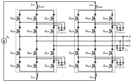
Figure 1.
Parallel three-phase FCC-CSC system topology.
In this paper, a parallel FCC-CSC structure is proposed to achieve higher rated power by simultaneously increasing the system voltage and current ratings. A three-segment interleaved SVM strategy for achieving five-level current output is introduced to enhance the AC output power quality of the system. Meanwhile, an optimized zero-state replacement (ZSR) based FC voltage control strategy is proposed to achieve voltage balancing among series-connected devices. Additionally, a sub-DC bus current balance strategy utilizing redundant switching states is designed. In summary, the parallel FCC-CSC system can achieve better AC output quality, excellent device voltage balancing performance, and DC bus current balancing. Simulation and experimental results validate the effectiveness of the proposed methods.
2. Operation Principle and Modulation Strategy of Parallel FCC-CSC
The inclusion of FCs in the FCC-CSC structure provides new commutation paths for the current, allowing the series-connected switches in the same half-bridge to operate asynchronously. This results in more switching state combinations and theoretically enables FC voltage control. Additionally, the parallel FCC-CSC structure can enhance the system’s rated current and improve the harmonic performance on the AC side. In this section, the operation principle of the parallel FCC-CSC system will be specifically introduced. Furthermore, an interleaved SVM modulation strategy will be presented to enhance the output power quality of the parallel FCC-CSC system.
2.1. Operation Principle Analysis
In the topology shown in Figure 1, the FCC-CSC is divided into upper and lower bridge arms, each half-bridge is consisted with two series-connected devices and two series-connected diodes. Similar to the traditional CSC topology, to ensure the magnitude of the output current vector is determined, only one set of bridge arms (one upper and one lower) is allowed to conduct at any given time. However, in the FCC-CSC topology, a set of three-phase filter capacitors is connected in parallel between the two series-connected switches of the same half-bridge, providing a new current path within the bridge arm. This means that the two switches of the same half-bridge do not have to act simultaneously. The switches in the FCC-CSC structure can be divided into two groups: the six switches near the output end and the six switches near the DC bus, referred to as the odd group and the even group, respectively. Based on the switching state constraints of the traditional CSC, the gate signal constraints for the FCC-CSC can be derived as:
In the upper half-bridge, the switches Sap1/3, Sap2/4, Sbp1/3, Sbp2/4, Scp1/3, Scp2/4 are used, while in the lower half-bridge, the switches San1/3, San2/4, Sbn1/3, Sbn2/4, Scn1/3, Scn2/4 are employed. At the same time, regardless of the states of the even group switches, the output current is entirely determined by the states of the odd group switches. The states of the even group switches will influence the current paths through the FC. Figure 2 shows different kinds of current loops corresponding to different even group switch choices when Sap1 is on. When Sap1 and Sap2 are both on, the current does not flow through the FC, and thus the FC is not involved in charging or discharging, keeping the capacitor voltage constant. When Sap1 and Sbp2 are both on, FC(CFa1) will discharge, while FC(CFb1) will charge. Therefore, the FC voltage can be controlled without affecting the output current by designing the states of the even group switches. The impact of different switching states on the FC voltage is listed in Table 1. Where “↑” represents the FC voltage rise, and “↓” represents the FC voltage fall. It is important to note that the FC voltage and the output voltage will entirely determine the blocking voltage of each set of switches. For instance, in Figure 2a, with Sap1 and Sap2 conducting, they do not bear the blocking voltage. The blocking voltage of the remaining switches is given by the following expression:
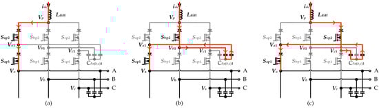
Figure 2.
Current commutation circuit when Sap1 is on (a) with Sap2 on (b) with Sbp2 on (c) with Scp2 on.

Table 1.
FC voltage variation rule.
Here, Va1, Vb1 and Vc1 are the clamping voltages of the FC, Va, Vb and Vc are the three-phase output voltages of the FCC-CSC, and Vp is the DC bus voltage. The derivation for the other modes is similar and will not be repeated here. The blocking voltage of the switches can be arbitrarily allocated through FC voltage control without affecting the output voltage. When switches with the same voltage rating are connected in series, the FC voltage can be controlled to be half of each phase output voltage. In this case, the blocking voltage of each switch is equal and clamped to half of the line voltage.
2.2. Interleaved SVM Modulation Strategy
As described in the previous section, the output voltage of the FCC-CSC system is entirely determined by the states of the odd group switches, while the FC voltage is controlled by the states of the even group switches. Therefore, these two control processes can be considered decoupled, as illustrated in Figure 3. For controlling the output with the odd group switches, the traditional CSC-SVM modulation strategy can be employed. Once the states of the middle six switches are determined, the appropriate states of the even group switches can be selected based on the results tabulated in Table 1, along with the current FC voltage state, to achieve flexible adjustment of the FC voltage.
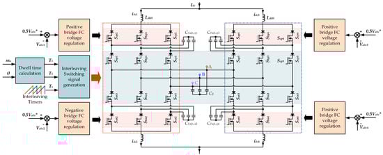
Figure 3.
Output and FC voltage regulation process of parallel FCC-CSC system.
Taking the traditional three-segment SVM with the minimum number of switching actions as an example, the reference current vector will be synthesized by two adjacent active vectors and one zero vector within one PWM period. It is worth noting that the choice of zero vector depends on the performance metrics of interest. For instance, in Sector I, the dwell time of each vector are as follows:
where T1, T2 and T0 are the dwell time of the two active vectors and the zero vector, respectively, ma is the modulation index, and θ is the reference angle within each sector.
For the parallel FCC-CSC system, the total output current can be defined as:
where idc1 and idc3 are the upper DC bus currents of each module, and idc2 and idc4 are the lower DC bus currents. Assuming these DC currents can be divided into half of the bus DC current, the above equation can be simplified as follows:
Figure 4 illustrates the PWM diagram of the designed interleaved three-segment SVM. By comparing the triangular carrier with the calculated duty cycles, the digital implementation of SVM can be achieved. The sequence of vector application can be flexibly designed to achieve multiple objectives, such as harmonic performance and switching loss. For parallel modules, two different timers with a half-cycle phase shift are used as carriers, and they share the vector dwell times. As a result, the two modules will produce interleaved three-level current outputs, and the combined output will present a five-level output.
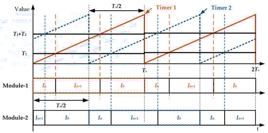
Figure 4.
Interleaved SVM diagram.
Figure 5a shows the PWM current waveforms of a single and a parallel FCC-CSC. The parallel FCC-CSC system can increase the current levels through interleaved SVM, thereby improving the quality of the output power. The harmonic analysis of the output currents for a single and a parallel FCC-CSC is shown in Figure 5b. Compared with the single FCC-CSC system, the parallel FCC-CSC system with interleaved SVM has improved output harmonics over the entire modulation index range. Moreover, the improved output power quality will further enhance the FC voltage control performance according to the analysis.
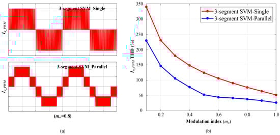
Figure 5.
(a) Output current schematic of single and parallel FCC-CSC systems. (b) harmonic analysis of single and parallel FCC-CSC systems.
3. FC Voltage Control Based on an Optimized ZSR with DC Current Balance
For the parallel FCC-CSC system sharing a common DC bus, it is crucial to address the current balance issue among the sub-DC buses. Unbalanced currents can increase circulating current, degrade output quality, and even damage the system. In this section, an FC voltage control strategy based on an optimized ZSR is introduced. Following that, a current balancing strategy is proposed that utilizes redundant switching states.
3.1. FC Voltage Control Based on an Optimized ZSR
In addition to achieving current balance, a more crucial task for the even group switches is to control the FC voltage to ensure the voltage balance of the switches. In the practical operation of the FCC-CSC system, the output and FC line voltages are often sampled. To avoid complex calculations, the line voltage is directly used as the feedback variable for control. During operation, when the FC line voltage is less than half of the output line voltage, it is recorded as logic “0”. When the FC line voltage is larger than half of the output line voltage, it is recorded as logic “1”. There are 8 combinations for the three-phase logic ranging from [000] to [111]. However, since the FC line voltages are star-connected and follow the three-phase symmetry principle, the situation where all three-phase FC line voltages are either larger than or less than half of the output line voltage will not occur. Therefore, there are only 6 possible cases for the relationship between the FC voltage and the output line voltage, labeled as [001] to [110], and referred to as Case 1 to Case 6.
From the analysis in Table 1, it can be derived that the selection of the even group switch states depends on the current case and the states of the odd group switches. Figure 6 illustrates the selection of the even group switch states for each case when Sap1/3 is on. Figure 7 shows the FC voltage regulation diagram when using the traditional three-segment SVM modulation.
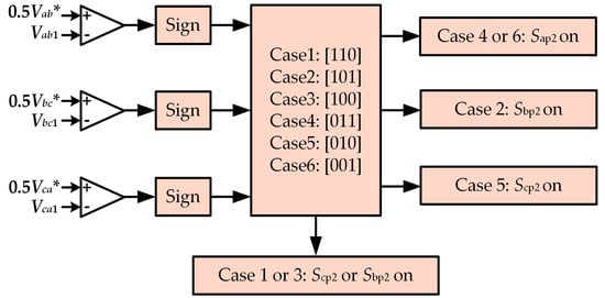
Figure 6.
The even-group switches corresponding to each Case are selected when Sap1/3 is on.
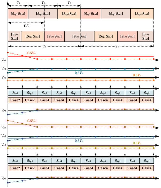
Figure 7.
Performance of FC voltage control under traditional three-segment SVM.
As shown in Figure 7, the FC voltage control does not achieve the expected regulation around the reference value, especially the C-phase FC voltage (Vc1), which becomes completely uncontrolled within the entire sector. This is because in Sector I, Sap1 remains continuously on, limiting the available switching states for effective FC voltage control.
To address the aforementioned issue, an optimized ZSR strategy is proposed to enhance FC voltage control performance. The specific replacement principles are shown in Table 2. The performance of FC voltage control under three-segment SVM modulation with an optimized ZSR is illustrated in Figure 8. It can be observed that the zero vector [Sap1/3 San1/3] is replaced by [Scp1/3 Scn1/3]. This allows the FC voltage to be regulated around the reference voltage effectively.
Table 2.
Traditional and optimized ZSR principles.
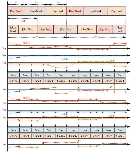
Figure 8.
Performance of FC voltage control under three-segment SVM with an optimized ZSR.
3.2. Current Analysis and Sharing Strategy of DC Bus in Parallel FCC-CSC System
In this section, the circulating current phenomenon in the parallel FCC-CSC system is ignored, assuming that the upper DC bus current and the lower DC bus current of each module are equal. Figure 9 depicts the upper bridge topology and the simplified model of the parallel FCC-CSC system. The DC link current of each module is essentially the current flowing through the differential inductors. According to the characteristics of inductive components, we can derive Equation (6).
where Vp1 and Vp3 are the DC side voltages of the two modules, and Vp is the voltage at the common terminal of the differential inductors. Further, the difference in the DC bus currents of each module in the parallel FCC-CSC system can be expressed as (7):
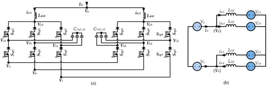
Figure 9.
DC bus current analysis (a) Upper bridge topology (b) Simplified DC circuit.
Thus, the difference in DC bus currents is related to the sub-DC bus voltage of each module, and the sub-DC bus voltage of each module corresponds to the state of the odd and even group switches. The relationship between the sub-DC bus voltage and the switching states is summarized in Table 3. Since the state of the odd group switches is determined by the desired current output, it cannot be adjusted arbitrarily. Therefore, the balance of the bus current can only be achieved by changing the switching state of the even group switches.
Table 3.
Sub-DC bus voltage of parallel FCC-CSC system.
During the modulation process, the waveforms of Vp1 and Vp3 have been illustrated in Figure 7 and Figure 8. Vp1 and Vp3 ideally remain equal without employing the optimized ZSR. In this scenario, the difference in current between the sub-DC buses is primarily due to the differences in the DC side inductors and windings, differences in the conduction voltage drops of the switches, and time delays in the gate signals among multiple CSCs. However, when the optimized ZSR is applied, significant differences appear in the waveforms of Vp1 and Vp3. This causes an inherent steady-state error in the currents of the two sub-DC buses, which needs to be addressed.
In Figure 6, there are redundant switch states besides the switch states used to control the FC voltage. Specifically, when the FC voltage is in Case 1 or Case 3, either Scp2/4 or Sbp2/4 can be chosen to conduct. Combining this with the results from Table 3, the corresponding sub-DC bus voltages for these two choices are different. This can be considered an additional degree of freedom in FC voltage control. Utilizing this characteristic, a current balance strategy can be designed as follows: When the FC voltage is in Case 1 or Case 3, first assess the current levels of the two sub-DC buses. Then, choose the switch state based on the corresponding sub-DC bus voltage of Scp2/4 and Sbp2/4. For example, if idc1 > idc3, select the switching state with the higher sub-DC bus voltage for Module 1 and the lower sub-DC bus voltage for Module 2. This approach can help mitigate the current imbalance between the sub-DC buses to some extent.
4. Simulation and Experimental Verification
This section presents the simulation and experimental validation of the parallel FCC-CSC system. The parameters are listed in Table 4. The interleaved SVM modulation introduced in Section 2, the FC voltage control strategy with the optimized ZSR and current balance function proposed in Section 3 were adopted. The carrier timer frequency was set to 4 kHz, and the FC voltage sampling frequency was set to 10 times the control frequency, which is 40 kHz in this section.
Table 4.
Simulation and experiment parameters.
4.1. Simulation Verification
Figure 10 and Figure 11 show the bus current simulation results of the two sub-modules before and after current balance, respectively, as well as the total error. In the simulation, the FCC-CSC system’s front end uses an ideal current source, and ideal components are employed to avoid the sub-DC bus current imbalance caused by component parameter errors. The total error is defined as follows:
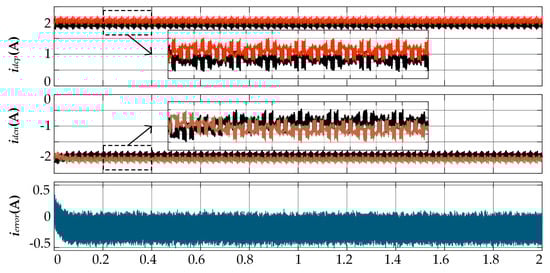
Figure 10.
Sub-DC bus current and error without DC current balance.
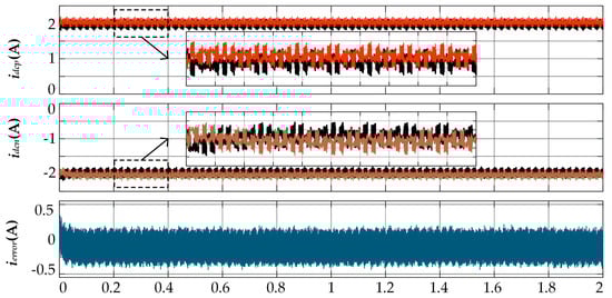
Figure 11.
Sub-DC bus current and error with DC current balance.
The simulation results are summarized in Table 5. Four indicators are used to describe the current quality of the sub-DC buses: the mean value for describing DC offset, the steady-state error M, the mean error EM, and the peak-to-peak value Vpp for describing ripple. With the inclusion of the current balancing strategy presented in this paper, the steady-state error M decreased by 41.2%, and the mean error EM decreased by 40.5%, validating the effectiveness of this strategy in combating DC offset in the sub-DC bus currents. Additionally, with the inclusion of the current balancing strategy, the peak-to-peak value Vpp of the sub-DC bus current also decreased by 3.8%, demonstrating that this method also has some effect in suppressing current ripple.
Table 5.
Sub-DC bus simulation results.
4.2. Experiment Verification
The experimental setup is shown in Figure 12, consisting of a DC current source and two FCC-CSC modules. The system status is sampled through sensor modules and fed back to the dSPACE system for computation. Control signals are then generated and sent out by the dSPACE system. The FCC-CSC-type switch is realized by the series-connected SiC MOSFET (C3M0032120K) and Diode (IDWD40G120C5).
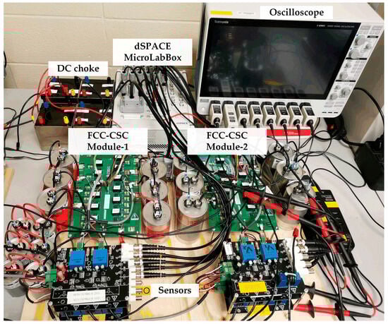
Figure 12.
Experiment setup of parallel three-phase FCC-CSC.
Figure 13 and Figure 14 show the experimental results of a single FCC-CSC and a parallel FCC-CSC, respectively. The output frequency is set to 60 Hz with a modulation index of 0.8. The total DC bus current for both systems is equal, resulting in output voltages and currents with identical amplitude and frequency. The experimental results show that, with the proposed interleaved SVM, the parallel FCC-CSC system significantly improves AC output quality compared to the single FCC-CSC system, effectively reducing voltage ripple. The total harmonic distortion (THD) of the output voltage decreased from 4.5% to 1.5%.
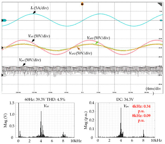
Figure 13.
Experimental results of single FCC-CSC system.
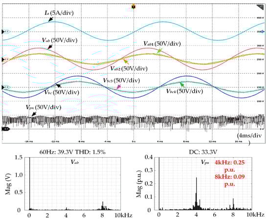
Figure 14.
Experimental results of parallel FCC-CSC system.
Moreover, the improved output voltage also facilitates FC voltage regulation because the output voltage serves as the reference value for FC voltage regulation. The DC bus voltage varies with the switching states of the even group switches, corresponding to the FC voltages of each phase. Therefore, the quality of the DC bus voltage benefits from the enhanced FC voltage control performance, showing improvement as well. From the experimental results, the primary harmonic content near 4 kHz in the bus voltage was reduced from 0.34 p.u. to 0.25 p.u.
In conclusion, the parallel FCC-CSC system with the proposed interleaved SVM modulation exhibits better power quality on both the AC and DC sides.
Furthermore, experiments comparing single FCC-CSC and parallel FCC-CSC configurations under different modulation indices were conducted. The results are depicted in Figure 15, illustrating that the parallel FCC-CSC system exhibits enhanced AC output harmonic performance across the entire range of modulation indices.
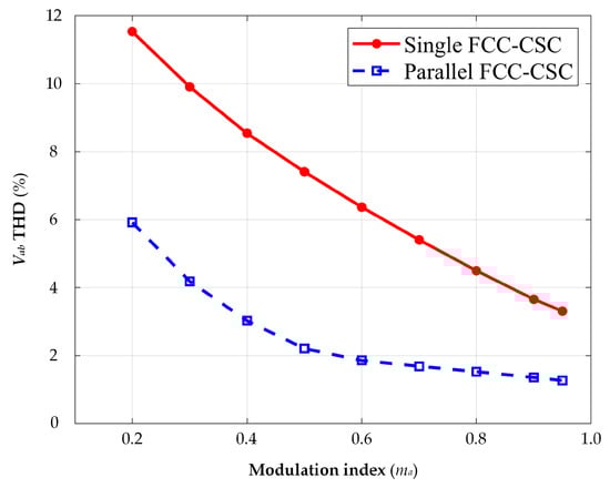
Figure 15.
Comparison of harmonic performance of output voltage in full modulation index range.
Additionally, dynamic performance experiments were conducted on the parallel FCC-CSC system, with results shown in Figure 16 and Figure 17. It can be seen that irrespective of changes in output frequency or modulation index, the proposed modulation method and FC voltage control strategy achieve robust performance. Throughout the transient process, the FC voltage can be actively controlled to half of the output voltage to prevent damage to series-connected devices due to voltage imbalance.
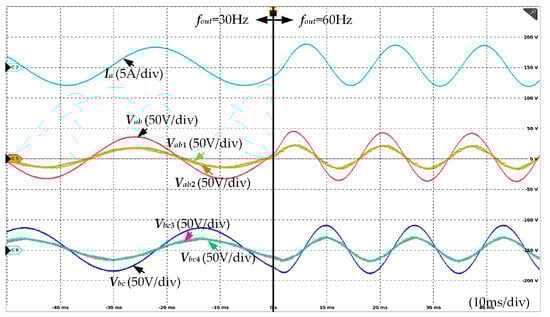
Figure 16.
Dynamic performance test of parallel FCC-CSC system—variable output frequency.
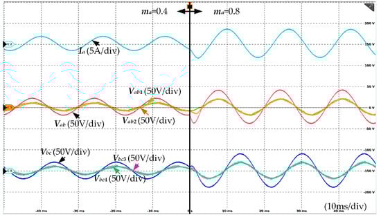
Figure 17.
Dynamic performance test of parallel FCC-CSC system—variable modulation index.
Finally, experiments were conducted to validate the sub-DC bus current equalization strategy, with results shown in Figure 18 and Figure 19. These figures respectively illustrate the balance of sub-DC bus currents when varying the total DC bus current and the AC output frequency. The experimental results demonstrate that under both scenarios, the sub-DC bus currents can evenly distribute the total DC bus current with minimal error. Furthermore, it is observed that the proposed current equalization strategy does not compromise the effectiveness of FC voltage control.
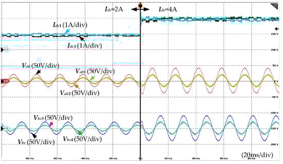
Figure 18.
Current sharing test of parallel FCC-CSC system—variable bus current.
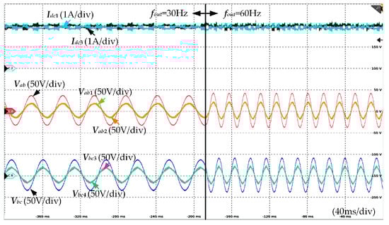
Figure 19.
Current sharing test of parallel FCC-CSC system—variable output frequency.
In summary, the FCC-CSC operating under this strategy exhibits independence and modularity, allowing for corresponding parallel operation designs. This advantage simplifies modulation and control strategies, considering the complexity of the system.
It is worth mentioning that, due to the limitation of experimental conditions, this part is the feasibility verification of the parallel FCC-CSC system in principle. Its application effect in high-power scenarios will be demonstrated in future work.
5. Discussion
The proposed parallel FCC-CSC system has improved rated voltage and current as well as enhanced AC and DC power quality, which is very suitable for application in the field of medium voltage power transmission. However, there are several areas where further work is needed. The first is whether the parallel operation of more modules can be realized. The parallel operation of multiple modules can greatly extend the rated current of the system, but the circulation problem between the FCC-CSC systems still needs to be further analyzed and suppressed. In addition, the current FCC-CSC topology only achieves voltage sharing of two series devices. In the application of higher bus voltage, can the FCC-CSC topology be extended to the series operation of three or more devices? At this time, the circuit modes will be more and more complex, and the FC voltage control strategy needs to be redesigned. Finally, the proposed FC voltage control strategy as well as the sub-DC bus current sharing strategy are based on the selection of redundant switching states, which seems to coincide with model predictive control (MPC). In the next step, the MPC theory can be added to the FC voltage control and sub-DC bus current sharing control, in order to seek better control effect.
6. Conclusions
This paper thoroughly investigates the parallel FCC-CSC system, making the following main contributions:
- The operation principle of the parallel FCC-CSC system is analyzed. Moreover, an interleaved SVM is proposed to achieve five-level current output, thereby enhancing the harmonic performance of the output voltage. Improved output voltage quality facilitates FC voltage control and further enhances the quality of the DC bus voltage.
- An optimized ZSR-based FC voltage control strategy is proposed, enabling effective FC voltage control within a three segment SVM framework. Compared to traditional five segment SVM modulation, this approach achieves lower equivalent switching frequencies for FC voltage control.
- Addressing the issue of unbalanced sub-DC bus currents in the parallel FCC-CSC system by proposing a current balance strategy utilizing redundant switch states. This strategy reduces steady-state error in sub-DC bus currents without compromising FC voltage control effectiveness, thereby enabling modularity in FCC-CSC systems.
Experimental and simulation results extensively validate the above conclusions.
Author Contributions
Methodology, X.C.; Resources, Q.G.; Software, S.W. and X.C.; Supervision, D.X. All authors have read and agreed to the published version of the manuscript.
Funding
This research received no external funding.
Data Availability Statement
Data are contained within the article.
Conflicts of Interest
The authors declare no conflicts of interest.
References
- Wang, Z.; Wu, B.; Xu, D.; Zargari, N.R. A Current-Source-Converter-Based High-Power High-Speed PMSM Drive with 420-Hz Switching Frequency. IEEE Trans. Ind. Electron. 2012, 59, 2970–2981. [Google Scholar] [CrossRef]
- Xia, Y.; Ahmed, K.H.; Williams, B.W. A PWM Current Source-Based DC Transmission System for Multiple Wind Turbine Interfacing. IEEE J. Emerg. Sel. Top. Power Electron. 2014, 2, 784–796. [Google Scholar]
- Alskran, F.; Simões, M.G. Multilevel Current Source Converter-Based STATCOM Suitable for Medium-Voltage Applications. IEEE Trans. Power Deliv. 2021, 36, 1222–1232. [Google Scholar] [CrossRef]
- Xu, F.; Guo, B.; Xu, Z.; Tolbert, L.M.; Wang, F.; Blalock, B.J. Paralleled Three-Phase Current-Source Rectifiers for High-Efficiency Power Supply Applications. IEEE Trans. Ind. Appl. 2015, 51, 2388–2397. [Google Scholar] [CrossRef]
- Cardoso, J.; Vazquez, N.; Hernandez, C.; Vaquero, J. A Transformerless Single-Phase Current Source Inverter Topology and Control for Photovoltaic Applications. Energies 2018, 11, 2011. [Google Scholar] [CrossRef]
- Yang, H.; Tu, R.; Wang, K.; Lei, J.; Wang, W.; Feng, S.; Wei, C. A Hybrid Predictive Control for a Current Source Converter in an Aircraft DC Microgrid. Energies 2019, 12, 4025. [Google Scholar] [CrossRef]
- Kroplewski, P.; Morawiec, M.; Jąderko, A.; Odeh, C. Simulation Studies of Control Systems for Doubly Fed Induction Generator Supplied by the Current Source Converter. Energies 2021, 14, 1511. [Google Scholar] [CrossRef]
- Fu, T.; Gao, J.; Liu, H.; Xia, B. Research on the Control and Modulation Scheme for a Novel Five-Switch Current Source Inverter. Energies 2024, 17, 3640. [Google Scholar] [CrossRef]
- Lin, X.; Ravi, L.; Zhang, Y.; Burgos, R.; Dong, D. Analysis of Voltage Sharing of Series-Connected SiC MOSFETs and Body-Diodes|IEEE Journals & Magazine|IEEE Xplore. Available online: https://ieeexplore.ieee.org/abstract/document/9286515 (accessed on 16 July 2024).
- Belverde, G.; Galluzzo, A.; Melito, M.; Musumeci, S.; Raciti, A. Snubberless Voltage Sharing of Series-Connected Insulated-Gate Devices by a Novel Gate Control Strategy. IEEE Trans. Power Electron. 2001, 16, 132–141. [Google Scholar] [CrossRef]
- Ding, L.; Li, Y.; Li, Y.W. A New Current Source Converter Using AC-Type Flying-Capacitor Technique. IEEE Trans. Power Electron. 2021, 36, 10307–10316. [Google Scholar] [CrossRef]
- Ding, L.; Li, Y.; Li, Y.W. Three-Phase Flying Capacitor Clamped Current Source Converter with Active Capacitor Voltage and CMV Control. IEEE Trans. Ind. Electron. 2022, 69, 13011–13021. [Google Scholar] [CrossRef]
- Guzman, J.I.; Melin, P.E.; Espinoza, J.R.; Moran, L.A.; Baier, C.R.; Munoz, J.A.; Guinez, G.A. Digital Implementation of Selective Harmonic Elimination Techniques in Modular Current Source Rectifiers|IEEE Journals & Magazine|IEEE Xplore. Available online: https://ieeexplore.ieee.org/abstract/document/6248700 (accessed on 16 July 2024).
- Alskran, F.; Simões, M.G. Current Balancing Algorithm for Three-Phase Multilevel Current Source Inverters. Energies 2020, 13, 860. [Google Scholar] [CrossRef]
- Ding, L.; Li, Y.W. Simultaneous DC Current Balance and CMV Reduction for Parallel CSC System with Interleaved Carrier-Based SPWM. IEEE Trans. Ind. Electron. 2020, 67, 8495–8505. [Google Scholar] [CrossRef]
- Popat, M.; Wu, B.; Liu, F.; Zargari, N. Coordinated Control of Cascaded Current-Source Converter Based Offshore Wind Farm. IEEE Trans. Sustain. Energy 2012, 3, 557–565. [Google Scholar] [CrossRef]
- Wei, Q.; Wu, B.; Xu, D.; Zargari, N.R. Further Study on a PWM Current-Source-Converter-Based Wind Energy Conversion System Considering the DC-Link Voltage. IEEE Trans. Power Electron. 2019, 34, 5378–5387. [Google Scholar] [CrossRef]
- Cossutta, P.; Aguirre, M.P.; Engelhardt, M.A.; Valla, M.I. Control System to Balance Internal Currents of a Multilevel Current-Source Inverter. IEEE Trans. Ind. Electron. 2018, 65, 2280–2288. [Google Scholar] [CrossRef]
- Ding, L.; Li, Y.W. Simultaneous DC Current Balance and Common-Mode Voltage Control with Multilevel Current Source Inverters. IEEE Trans. Power Electron. 2018, 33, 9188–9197. [Google Scholar] [CrossRef]
- Barresi, M.; De Simone, D.; Piegari, L.; Scalabrin, R. Novel Current Source Converter for Integrating Multiple Energy Storage Systems. Energies 2024, 17, 2495. [Google Scholar] [CrossRef]
- Bai, R.; Zhao, B.; Zhou, T.; Wang, J.; Ma, Y.; Lin, G.; Wang, Y.; Yu, Z.; Zeng, R. Step-Current-Approximation Modulation of Multilevel-CSC with Near-Power-Frequency Switching for High-Current Variable-Voltage Application. IEEE Trans. Power Electron. 2023, 38, 11069–11079. [Google Scholar] [CrossRef]
Disclaimer/Publisher’s Note: The statements, opinions and data contained in all publications are solely those of the individual author(s) and contributor(s) and not of MDPI and/or the editor(s). MDPI and/or the editor(s) disclaim responsibility for any injury to people or property resulting from any ideas, methods, instructions or products referred to in the content. |
© 2024 by the authors. Licensee MDPI, Basel, Switzerland. This article is an open access article distributed under the terms and conditions of the Creative Commons Attribution (CC BY) license (https://creativecommons.org/licenses/by/4.0/).