Abstract
This paper investigates the commutation transients of MOSFET and GaN FET devices in motor drive applications during hard-switching and soft-switching commutations at dead time operation. This study compares the switching behaviors of MOSFETs and GaN FETs, focusing on their performance during dead time in inverter legs for voltage source inverters. Experimental tests at various phase current levels reveal distinct switching characteristics and energy dissipation patterns. A validated simulation model estimates the experimental energy exchanged and dissipated during switching transients. The results demonstrate that GaN FETs exhibit lower overall losses at shorter dead times compared to MOSFETs, despite higher reverse conduction voltage drops. The study provides a quantitative framework for selecting optimal dead times to minimize energy losses, enhancing the efficiency of GaN FET-based inverters in low-voltage motor drive applications. Finally, a dead time optimization strategy is proposed and described.
Keywords:
motor drive; inverter leg; dead time; switching losses; reverse conduction; GaN FET; MOSFET 1. Introduction
The performance limitations of silicon-based power devices are increasingly evident, moving the semiconductor industry towards alternative materials like silicon carbide (SiC) and gallium nitride (GaN). GaN, in particular, has gained significant traction due to its superior switching speed capabilities [1,2]. Traditional silicon power MOSFETs have faced challenges in balancing conduction and switching losses, as efforts to reduce on-resistance often result in increased parasitic capacitances, leading to higher switching losses [3].
In Pulse-Width Modulation (PWM) motor drive applications, the adoption of GaN technology offers the potential to achieve higher switching frequencies, which in turn reduces torque ripple and improves the waveform quality of the motor current [4]. In a motor drive powered by a voltage source inverter, the dead time is necessary to avoid cross-conduction [5]. Unfortunately, dead time always causes the waveform distortion phenomenon in a motor drive, and dead time compensation strategies are required [6]. Moreover, voltage source inverters used in these applications require dead time to prevent cross-conduction, introducing waveform distortion. This distortion originates from the inherent delays in switching devices and the characteristics of the devices themselves, such as turn-on and turn-off delays and reverse conduction voltage drop [7].
GaN FETs are particularly attractive in power electronics due to their low on-resistance and ability to operate at very high frequencies [8]. For low-voltage (V < 100 V) motor drives, GaN FET-based inverters have demonstrated advantages in reducing the size of passive components and minimizing motor current distortion and torque ripple. On the other hand, an advanced motor insulation layout and a deep investigation of the commutation transient in the inverter leg are required due to the dV/dt increase [9].
Properly setting the dead time is crucial to minimize both reverse conduction [10]. Numerous studies have aimed to optimize dead time settings, exploring solutions like gate driver ICs with adjustable or adaptive dead time capabilities. While some methods, such as programmable dead time settings, lack adaptability in real-world applications [11], others have shown promise but often lack generality or theoretical underpinning [12,13]. Recent research has highlighted the importance of theoretically derived optimal dead time values, which have demonstrated improvements in efficiency [14]. These research studies require a deep knowledge of the considered device behavior, depending on the operative conditions and the technology features [15,16].
This paper investigates the commutation transients of MOSFET and GaN FET devices during dead time for motor drive applications. Experimental tests are conducted in an inverter leg board controlling the phase current. Results reveal different switching behaviors depending on the working conditions. The energy exchanged between the high-side and low-side devices during commutations and the energy losses are estimated through a validated model of the system. The contribution to switching losses during hard-switching and soft-switching commutations and the differences between GaN FET and MOSFET results are distinguished and deeply investigated. Findings aim to provide insights and guidelines for optimizing dead time based on the specific technology for different operating conditions. Furthermore, an optimization strategy for the dead time related to the GaN FET in inverter leg application is presented and described.
2. GaN FET and MOSFET Commutation Transients in Motor Drive Application
The motor drive system used consists of a GaN FET-based inverter powering a 3-phase permanent magnet (PM) motor. Figure 1 shows the system composed of the inverter and the electrical machine. The inverter is composed of three legs, one for each motor phase. The stator phase currents , , are controlled by the high-side and the low-side using a Pulse-Width Modulation (PWM). The modulation works at the switching frequency , significantly higher than the AC stator phase current frequency of the motor in order to ensure control stability. A dead time () is introduced between the devices’ commutation in which both driving signals are off-state. This is set by the user to avoid shoot-through in the inverter leg [17]. Nevertheless, the introduction of creates voltage harmonic distortion affecting the phase current waveform [18,19].
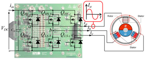
Figure 1.
A 2-Level inverter using GaN FETs powering a 3-phase AC permanent magnetic motor.
In AC motor drive systems, each inverter leg operates with a sinusoidal phase current of various amplitudes. These currents are directed either from the inverter leg’s switching node to the motor phase or in the reverse direction. Figure 1 shows that a current entering the stator phase is considered positive.
To study commutation transients in switching legs with MOSFET and GaN FET devices, we used two half-bridge experimental board PCBs. These boards only differed in device technology. This setup ensured consistent parasitic effects from the PCB, allowing a fair comparison. Nevertheless, the different packages of GaN FET and MOSFET cannot be removed. However, the choice of the technology leads to the use of the corresponding parasitic elements introduced by the case of the selected device [20,21]. Moreover, tests are carried out using equal operating conditions for both the GaN FET-based board and the MOSFET-based one.
The GaN FET board featured EPC2065 GaN FET, while the MOSFET one featured Onsemi FDMS2D5N08C. The device features are reported in Table 1.

Table 1.
MOSFET Onsemi FDMS2D5N08C and GaN FET EPC2065 features.
Figure 2a depicts the schematic of the inverter leg. Figure 2b,c show the pictures of the GaN FET board and the MOSFET one, respectively.
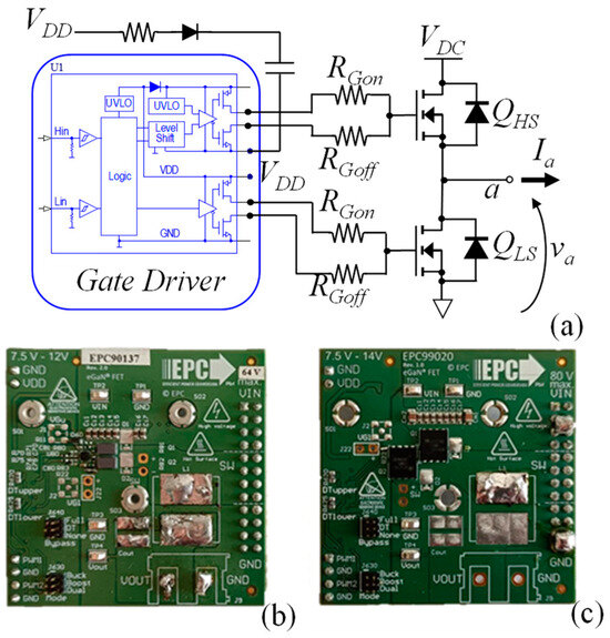
Figure 2.
(a) Electric schematic of the half-bridge boards used for testing the devices. (b) GaN FET-based board. (c) MOSFET-based board.
Precise measurement results are particularly challenging to obtain, especially when they aim to distinguish different events that happen in a short time (e.g., during the switching transient of WBG devices). Therefore, a dedicated experimental setup controlling the system variables is required [22].
Testing occurred at an ambient temperature of 25 °C with a DC input voltage of . A second inverter board is used to control the phase current connecting an LCL filter to the half-bridge switching node (point a of Figure 2a). An STM32H7 microcontroller generated PWM signals and controlled the phase current. The PWM operated at a switching frequency with a duty cycle of 0.1 to reduce current ripple. This is sufficient to ensure that the switching transient has been completed before a new switching. Despite the fact that WBG devices can operate at a higher switching frequency, the selection does not affect the switching transient’s investigation [23]. Additionally, is a reasonable settlement for the MOSFET, which operates at a lower than the GaN FET; duration needs to be chosen long enough to prevent shoot-through and obtain hard-switching for commutations with low phase current [24]. Furthermore, significant distortion effects due to the duration of the dead time need to be avoided [25]. In the experimental test, both GaN FET and MOSFET boards have a dead time of which is a good trade-off between the GaN FET and MOSFET requirements. During , transitioning from high-side () turn-off to low-side () turn-on can cause zero-voltage transients at different current levels [26].
Experimental tests carried out with reveal that the MOSFET switching leg achieves zero voltage switching (ZVS) [27] for currents . The GaN FET achieves ZVS at lower .
The voltage waveforms are measured using a digital scope featuring a bandwidth of 500 MHz, an output resistance of 10 MΩ, and an output capacitance of 10 pF.
The experimental setup of the controlled current-level system is shown in Figure 3. It includes the half-bridge board under test, the power converter regulating , and the STM32H7 microcontroller.
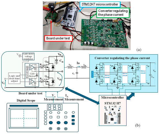
Figure 3.
Experimental setup made of the half-bridge board under test (GaN FET and MOSFET), the converter imposing the phase current, and the STM32H7 microcontroller. (a) Picture of the testing bench, (b) block diagram of the experimental setup.
Tests are conducted for positive current values (exiting from the switching node and entering the converter regulating current) at . Two commutation characteristics for two transitions are analyzed:
- High-Side Turn-Off, Low-Side Turn-On: This commutation features a negative voltage slew rate () as the switching node voltage () decreases;
- Low-Side Turn-Off, High-Side Turn-On: This had a positive voltage slew rate () as the switching node voltage () increased to .
The experimental test result achieved in these two commutations for various amplitudes are each reported separately.
2.1. Commutation with and Positive
Figure 4 shows the voltage waveforms measured on the half-bridge boards using GaN FETs and MOSFETs. Figure 4a displays the switching node voltage , while Figure 4b illustrates the gate-source voltages for the high-side device () and the low-side device (). The waveforms correspond to the current amplitudes indicated by the arrows.
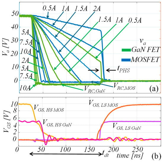
Figure 4.
Voltages measured on GaN FET and MOSFET during the turn-off and turn-on commutation with (). (a) Switching node voltage . (b) Gate-source voltages .
Depending on the length and the , three different switching events can happen for the switching node voltage:
- Zero voltage switching (ZVS);
- Voltage variation and partial hard switching (PHS);
- Voltage fall transient and reverse conduction (RC).
When the high-side switch () turns off, starts to fall. The rate of decline is steeper with higher due to the parasitic output capacitances of the devices () and the load [28]. Since is not constant with voltage, the dynamics of can be described using an equivalent capacitance . This is derived as the average value resulting from the slew rate () measured at different amplitudes and considering the time () taken for to fall to 0 V when turns off. Integrating the constitutive equation of a capacitance (), it is possible to calculate as
ZVS occurs when the low-side switch () turns on exactly as reaches 0 V. This is the condition in which . As shown in Figure 4, ZVS for MOSFET happens at a phase current amplitude of , while for GaN FET, it occurs between and . The GaN FET has a lower , compared to the MOSFET’s . The lower of the GaN FET results in a shorter , enabling ZVS at lower compared to the MOSFET.
When is lower than the ZVS threshold, a PHS event follows the transient. In this case, turns on before has fully dropped to 0 V. After , falls to ’s conduction value within the partial hard switching duration time (), causing PHS losses. Figure 4 shows MOSFET experiencing PHS at and , while the GaN FET exhibits PHS only at .
In the cases of higher values than those required for ZVS, drops to 0 V before ends . Subsequently, operates in RC mode until turns on. The reverse conduction duration is . is negative at due to the activation of the body-diode in the MOSFET or the equivalent diode behavior in the GaN FET. The reverse conduction voltage is higher for GaN FET () than for MOSFET (), causing higher RC losses in the GaN FET than in the MOSFET. No losses follow as turns on.
In Figure 5a are highlighted and in the example of the PHS event achieved with the GaN FET with . Figure 5b indicates the time intervals of and relative to the curves achieved with for the GaN FET.
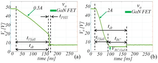
Figure 5.
Switching node voltages measure on GaN FET during the turn-off and turn-on commutation: (a) PHS event at ; (b) RC event at . .
2.2. Commutation with and Positive
Figure 6 shows voltage waveforms with for both the half-bridge board using GaN FETs and the one using MOSFETs at the same current variations as in Figure 4. Figure 6a presents the switching node voltage , while Figure 6b illustrates the gate-source voltages ( for the low-side device and for the high-side device).
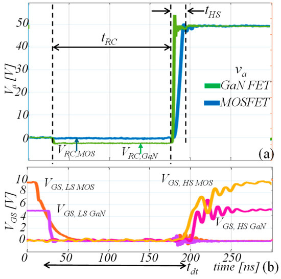
Figure 6.
Voltages measured on GaN FET and MOSFET during the turn-off and turn-on commutation with (). (a) Switching node voltage . (b) Gate-source voltages at the bottom side. .
The phase voltage waveforms rise with no differences for all amplitudes used in the tests. The difference in is determined by the device technology. The parasitic capacitance of the device affects the voltage rise time . The reverse conduction (RC) phase begins when turns off and ends when turns on. During RC, due to the body-diode of the MOSFET or the equivalent diode in the GaN FET. A hard switching (HS) event follows the dead time, lasting a few nanoseconds, and is a dissipative process because of equals .
2.3. Commutation with and Negative
The results for negative current are dual to those with positive current. The switching event of and is characterized by an RC phenomenon lasting . During RC, reaches the value of . Consequently, an HS event with a rapid rising happens, and it elapses in lasting a few nanoseconds (). All considerations made for and (Section 2.2) are valid.
Figure 7 illustrates measured on the boards with GaN FETs and MOSFET during the commutation with when testing with . Figure 7a depicts the falling waveforms, while Figure 7b shows the gate-source voltages for and ( for the low-side device and for the high-side device).
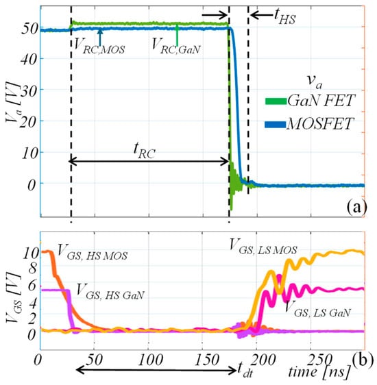
Figure 7.
Voltages measured on GaN FET and MOSFET during the turn-off and turn-on commutation with (). (a) Switching node voltage . (b) Gate-source voltages. .
2.4. Commutation with and Negative
For and , the commutation dynamics are influenced by the parasitic capacitance. Depending on the amplitude of , Zero Voltage Switching (ZVS), Partial Hard Switching (PHS), and Reverse Conduction (RC) events can occur. The same considerations discussed for and apply here. At higher amplitudes, the voltage rise time () is shorter. Figure 8 shows the voltages measured on GaN FET and MOSFET boards with during commutation with . Figure 8a illustrates the rising waveforms, while Figure 8b presents the gate-source voltages for and ( and , respectively).
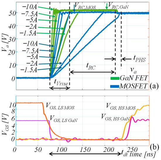
Figure 8.
Voltages measured on GaN FET and MOSFET during the turn-off and turn-on commutation with A (). (a) Switching node voltage . (b) Gate-source voltages . .
3. GaN FET vs. MOSFET Commutation Energy Evaluation
The board used for experimental tests does not incorporate current sensing to measure the current of transistors in a half-bridge configuration. This is intentionally designed to prevent any impact on the switching board’s performance. Nevertheless, measuring transistor current is crucial for evaluating power trends and energy during commutations. To achieve the current waveform of devices, LTSpice simulations are used. The simulation models for MOSFET and GaN FET are sourced from the manufacturer’s official websites.
The simulated electrical circuit replicates the experimental setup (see Figure 2a) and maintains the same operating conditions: ; and duty-cycle 0.1. The half-bridge circuit model is validated by ensuring it produces waveforms consistent with those obtained in the experimental tests, as depicted in Figure 4 and Figure 6 [29]. The phase currents exiting the switching node (positive ) in the simulations are , emulating the experimental conditions.
Simulations are performed twice with dead times and . These values are typical for the respective devices (20 ns for GaN FETs and 150 ns for MOSFETs) and are relevant for motor drive applications. The energy values computed from the simulations pertain to the low-side device ().
Figure 9 and Figure 10 show the waveforms of the current , the phase voltage and the power during the commutation with , load current of and a dead time of and with respectively. Figure 9a and Figure 10a refer to the GaN FET, while Figure 9b and Figure 10b refer to the MOSFET.
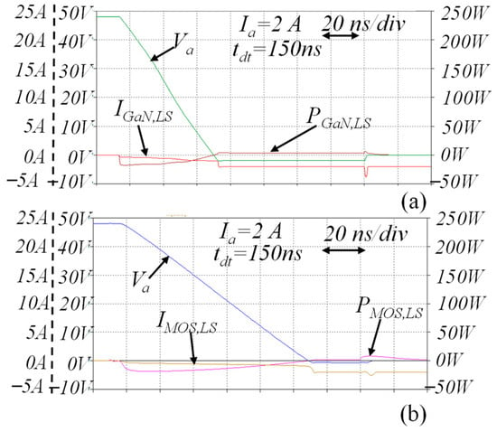
Figure 9.
Waveforms of the commutation with , and . (a) GaN FET ; ; power = 25 W/div. (b) MOSFET ; ; power = 25 W/div. .
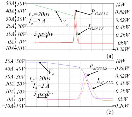
Figure 10.
Waveforms of the commutation with , and . (a) GaN FET ; ; power = 200 W/div. (b) MOSFET ; ; power = 200 W/div. .
Comparing the GaN FET waveforms of Figure 9a and Figure 10a with the MOSFET ones in Figure 9b and Figure 10b shows that the and current variations last longer in the MOSFET than in the GaN FET. As a result, during the fall the GaN FET power has a peak comparable with those of the MOSFET , but lasts shorter. In the case of soft switching following the fall in Figure 9a,b, GaN FET features a higher reverse conduction voltage drop (). The current flowing through the device operating in reverse conduction is and it is equal for both the GaN FET or the MOSFET. Therefore, the higher of the GaN FET leads to higher reverse conduction losses than the MOSFET [30]. Due to the higher voltage drop of the GaN transistor during reverse conduction operation, the device in the third quadrant must work with reduced timing to optimize performance and losses. In the hard-switching event with and shown in Figure 10a,b, the overall GaN FET hard switching losses are much lower than the MOSFET ones.
During the commutation exhibiting ( turning off and turning on) with a positive , it is possible to distinguish between the amplitudes that result in ZVS or RC and those that cause PHS. The energy of during the voltage variation, , is determined by the equation:
where is the current through and is the time taken for the switching node variation . The time varies according to the falling slew rate. If drops to 0 V before the end of , RC conditions appear. ZVS condition appears when equals the maximum value of if reaches 0 V at the end of . The PHS conditions occur if the theoretical voltage fall time exceeds . When is followed by RC conditions lasting , the energy losses during are denoted as and calculated as
where is the RC time interval when is negative and equal to for the GaN FET or MOSFET. The upper integral limit at is close to and includes turn-on delays of and the driving circuit’s propagation delay uncertainty.
If does not drop to 0 V within , the voltage variation during is followed by PHS. The energy losses due to the PHS are calculated as
where is the duration of the PHS phenomenon, starting at the end of and ending as .
In the ZVS condition, and . is the only energy involved in the switching event.
Figure 11 and Figure 12 illustrate the energies involved during the QHS turn-off and QLS turn-on with positive from 0.5 A to 10 A. Figure 11 refers to results with , while Figure 12 refers to those achieved with . In particular, Figure 11a and Figure 12a depict the energy as a function of . On the other hand, Figure 11b and Figure 12b show the energy losses due to RC () and PHS () as a function of . ZVS is marked with a dashed line, while PHS and RC are marked with dotted lines. MOSFET curves are blue, and GaN FET curves are green.
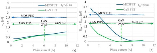
Figure 11.
Energies of (MOSFET in blue and GaN FET in green) versus phase current during the commutation with and using . (a) Energy of voltage variation; (b) PHS and RC energies. ZVS event is highlighted with a dashed line. PHS and RC are highlighted with dotted lines. ; .
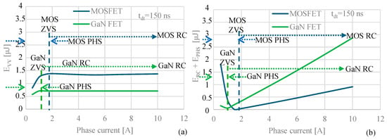
Figure 12.
Energies of (MOSFET in blue and GaN FET in green) versus phase current during the commutation with A and using (a) Energy of voltage variation; (b) PHS and RC energies. ZVS event is highlighted with a dashed line. PHS and RC are highlighted with dotted lines. ; .
GaN FET achieves ZVS at with and at with . Differently, the MOSFET achieves ZVS at with , while it does not achieve ZVS with for currents up to . RC losses occur for higher than the one causing ZVS, while PHS occurs for lower than the ZVS.
Commutation with starts with the initial conditions of of charged to and of discharged to nearly 0 V. Immediately after turning off , of discharges to 0 V and of charges to . During this, both devices are in the off-state, but the variation of causes an exchange of energy between them. The amount of exchanged varies depending on the switching event:
- ZVS or RC: of discharges of until stabilizes at 0 V, while of charges of up to . is maximum () since of fully discharges using the charging energy of of . is calculated as
- PHS: of does not discharge completely because after the phase voltage is not null, . of charges of , and of does not fully charge to . GaN FET’s smaller results in a steeper fall and a shorter for exchanging . As a result, MOSFET features a greater quantity of losses than the GaN FET when using the same .
ZVS condition features zero energy losses . Only is involved due to the energy exchange between the switching leg devices’ output capacitances ( and ). Differently, PHS and RC are dissipative phenomena following (Figure 11b and Figure 12b).
Considering the same , PHS energy losses is lower with long because turns on with a lower (closer to ZVS). Additionally, elapsed , GaN FET’s smaller results in a steeper fall than MOSFET, leading to lower for GaN FET. On the other hand, MOSFET features a lower voltage drop and corresponding losses than the GaN FET. increase proportionally with and whatever the technology is considered.
Figure 13 and Figure 14 show the GaN FET and MOSFET waveforms of the current , the phase voltage and the device power during the commutation with . Additionally, Figure 13a and Figure 14a show the GaN FET power , while Figure 13b and Figure 14b depict the MOSFET reverse recovery current and the body-diode power, respectively. In particular, Figure 13 refers to the case with and Figure 14 to .
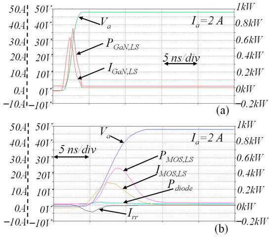
Figure 13.
Waveforms of the commutation with and . (a) GaN FET power . (b) MOSFET ; ; power ; reverse recovery current ; body-diode power . .
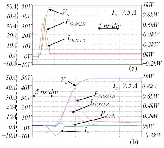
Figure 14.
Waveforms of the commutation with and . (a) GaN FET power . (b) MOSFET ; ; power ; reverse recovery current ; body-diode power . .
During commutation with ( turn off and turn on), the transient event starts with the of being discharged, and of being charged to . With positive , works in reverse conduction for all . At the end of , turns on with a drain-source voltage of , causing hard switching (HS). The device has a current peak and an almost instantaneous charge.
GaN FET waveforms in Figure 13a and Figure 14a exhibit negligible differences with the level. Furthermore, GaN FET shows a faster dynamic than the MOSFET one of Figure 13b and Figure 14b because of the low GaN FET . Additionally, MOSFET features a reverse recovery current due to the body-diode which causes an increase of in switching losses . A higher leads to a higher peak and higher , as shown comparing Figure 13b and Figure 14b. GaN FET does not feature reverse recovery current and corresponding losses. The peak is due only to the charging .
The reverse conduction energy achieved by both for GaN FET and MOSFET is illustrated in Figure 15a and Figure 16a as a function of . Figure 15b and Figure 16b depict the hard switching energy losses () as a function of . Figure 15 refers to the case with , while Figure 16 refers to the one with . GaN FET curves are depicted in green, while MOSFET curves are shown in blue.
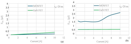
Figure 15.
Energies of (MOSFET in blue and GaN FET in green) versus phase current during the commutation with A and using . (a) Energy dissipation for reverse conduction ; (b) Energy dissipation for hard switching . .
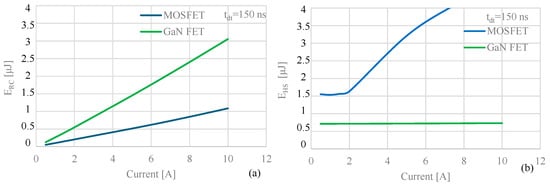
Figure 16.
Energies of (MOSFET in blue and GaN FET in green) versus phase current during the commutation with A and using . (a) Energy dissipation for reverse conduction ; (b) Energy dissipation for hard switching . .
The comparison of the GaN FET and MOSFET curves in Figure 15a and Figure 16a demonstrates that GaN FET losses are higher than MOSFET during due to higher [30]. Despite this, losses are significantly low (up to 0.3 μJ for GaN FET and 0.1 μJ for MOSFET) considering . ERC increases linearly with and the level of .
Figure 15b and Figure 16b show that HS energy losses of GaN FET are significantly lower than the MOSFET ones. GaN FET features a regardless of and . Differently, MOSFET, and EHS has a minimum for low levels which persist according to duration: for and for . corresponds to the energy required to charge the of to (no energy comes from of ) and it is calculated as
where is the constant equivalent value of (which is a non-linear parameter with the voltage). is not affected by and closely matches the maximum energy capacity of (), as arises comparing in Figure 12a and Figure 16b.
When level is higher, of the MOSFET grows with the amplitude, while the GaN FET one remains constant. The MOSFET increase is due to the additional reverse recovery charge in the MOSFET’s P-N junction, which grows with longer and higher reverse recovery current [31,32]. Conversely, the GaN FET maintains a constant due to the absence of a P-N junction, thereby featuring [33]. In general, significantly exceeds , particularly at . When considering both energy dissipation components, the GaN FET exhibits reduced energy losses during the switching transient, especially with a shorter dead time ().
4. Dead Time Reduction Strategy
A reduction switching losses strategy can be developed acting on the dead time length. In particular, it is aimed to set the dead time differently for the switching events of ( turn off and turn on) and ( turn off and turn on), according to the load current sign:
- : set
- : set
- c.
- : set
- d.
- : set
Where is the minimum dead time which ensures a safe switching event according to the gate propagation delay uncertainty; is the optimum dead time minimizing the reverse conduction duration. Furthermore, in motor drive applications, it may be useful to maintain between a maximum value and the minimum . The dead time is chosen according to the maximum admissible hard-switching losses and avoids increasing the total harmonic distortion (THD) in the phase motor current [33,34].
4.1. Operation with Constant Minimum Dead Time Conditions
When turning on GaN FET HS with a , case a, (see Figure 6) and GaN FET LS with , case d, (see Figure 7), reverse conduction phenomenon persists for all the dead time duration, regardless of the amplitude. Reverse conduction is minimized by simply setting the minimum duration (). The condition can be enabled after having monitored the sign and applied only for the turn-on transient of the corresponding GaN FET: HS turns on when ; LS turns on when .
4.2. Operation with Reduced Dead Time Conditions
The control strategy for turning on GaN FET LS when , case b, (see Figure 4), or GaN FET HS when , case c, (see Figure 8) requires a preliminary estimation of the optimum dead time . A comparator is used to monitor the drain-source voltage of the GaN FET to turn on, as depicted in the circuit schematic of Figure 17a. A constant reference voltage is set as a threshold. The comparator compares with a threshold reference value . The dead time control block in Figure 17a generates the driving signal when falls below , as shown in Figure 17b. Additionally, a maximum dead time value in the dead time control block is considered [35].
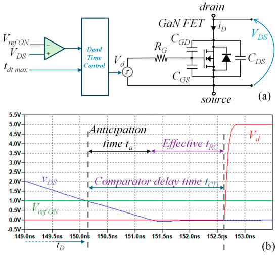
Figure 17.
(a) comparison and entering the dead time control strategy for dead time reduction. (b) Choice of for comparison. .
If VDS < is not triggered within the maximum dead time , the turn-on signal is generated regardless of the comparator output (the dead time is fixed and equal to ).
In Figure 17b, represents the turn-on driving time which corresponds to the time when the condition is triggered. The threshold is chosen according to the highest amplitude that does not cause reverse conduction within . This condition is equivalent to ZVS with . generation can be anticipated by the comparator delay time . is set equal to the value of when .
This approach ensures that the turn-on signal is sent only when the voltage variation has been completed, thereby minimizing reverse conduction. The commutation behavior is thus adapted to the current amplitude, differing from constant dead time methods.
4.3. Validation in Motor Drive Setup
For instance, the presented dead time reduction strategy is developed in a GaN FET-based inverter board supplying a BLDC motor (nominal voltage of 36 V, nominal power of 250 W, and 26 pole pairs). A maximum dead time of and a minimum of are selected. At the time the current in ZVS is 1.2 A. For the phase current below 1.2 A, the PHS condition appears. This td,mx value choice is a trade-off between the quality of the sinusoidal output current and reduced energy losses during the partial hard switching conditions (EPHS contribute).
The waveforms measured for utilizing the dead time reduction strategy are shown in Figure 18a for commutations with and in Figure 18b for commutations with .
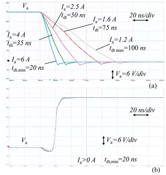
Figure 18.
waveforms measured for utilizing the dead time reduction strategy. (a) ; (b) ; .
The voltage fall in Figure 18a shows that with higher it is possible to minimize the reverse conduction phenomenon shortening the dead time. Moreover, for the dead time is maximum , while for the dead time is minimum . On the other hand, in Figure 18b, when rises with , the dead time is minimum independently from the amplitude.
5. Conclusions
This paper presents a comprehensive investigation into the commutation transients of MOSFET and GaN FET devices in motor drive applications, with a focus on hard-switching and soft-switching commutations. Through experimental tests and validated simulations, the study reveals distinct differences in switching behaviors and energy dissipation patterns between MOSFETs and GaN FETs. The key findings highlight that GaN FETs exhibit significantly lower overall losses at shorter dead times compared to MOSFETs, despite a higher reverse conduction voltage drop. Additionally, the lower output parasitic capacitance of GaN FETs contributes to faster commutations and reduced energy losses.
These insights provide a quantitative framework for optimizing dead time duration to minimize energy losses in GaN FET-based low-voltage inverters for motor drive applications. Furthermore, a strategy to optimize the dead time choice for the different operative conditions in the inverter leg is presented and described. The proposed strategy for dynamically adjusting dead time based on load conditions shows potential for further reducing commutation losses and enhancing inverter efficiency. Future research will focus on developing algorithms to adapt dead time duration in real-time, thereby optimizing performance and reducing energy consumption in motor drive systems.
Author Contributions
Conceptualization, S.M., M.P. and V.B.; methodology, V.B., S.M. and F.M.; software, V.B. and F.S.; validation, V.B., M.P. and F.S.; formal analysis, S.M., M.P. and F.M.; investigation, V.B., F.S. and M.P.; resources, M.P. and F.S.; data curation, S.M. and V.B.; writing—original draft preparation, S.M and V.B; writing—review and editing, M.P., F.M. and F.S.; visualization, V.B.; supervision, M.P. and S.M. All authors have read and agreed to the published version of the manuscript.
Funding
This research was funded by Project “Innovative Solutions for Renewables in Energy Communities (ISoREC)” through the Italian Ministry of University and Research (MUR) Progetti di Rilevante Interesse Nazionale (PRIN), Bando 2020 under Grant 202054TZLF.
Data Availability Statement
Data are contained within the article.
Conflicts of Interest
Author Marco Palma was employed by the Efficient Power Conversion Corporation. The remaining authors declare that the research was conducted in the absence of any commercial or financial relationship that could be construed as a potential conflict of interest.
References
- Meneghini, M.; De Santi, C.; Abid, I.; Buffolo, M.; Cioni, M.; Khadar, R.A.; Nela, L.; Zagni, N.; Chini, A.; Medjdoub, F.; et al. GaNbased power devices: Physics, reliability, and perspectives. J. Appl. Phys. 2021, 130, 181101. [Google Scholar] [CrossRef]
- Udabe, A.; Baraia-Etxaburu, I.; Diez, D.G. Gallium Nitride Power Devices: A State of the Art Review. IEEE Access 2023, 11, 48628–48650. [Google Scholar] [CrossRef]
- Baliga, J. Power semiconductor device figure of merit for high-frequency applications. IEEE Electron Device Lett. 1989, 10, 455–457. [Google Scholar] [CrossRef]
- Musumeci, S.; Mandrile, F.; Barba, V.; Palma, M. Low-Voltage GaN FETs in Motor Control Application; Issues and Advantages: A Review. Energies 2020, 14, 6378. [Google Scholar] [CrossRef]
- Chierchie, F.; Paolini, E.E.; Stefanazzi, L. Deadtime distortion shaping. IEEE Trans. Power Electron. 2019, 34, 53–63. [Google Scholar] [CrossRef]
- Li, Y.-S.; Wu, P.-Y.; Ho, M.-T. Dead-Time Compensation for Permanent Magnet Synchronous Motor Drives. In Proceedings of the 2020 International Automatic Control Conference (CACS), Hsinchu, Taiwan, 4–7 November 2020. [Google Scholar] [CrossRef]
- Liu, G.; Wang, D.; Jin, Y.; Wang, M.; Zhang, P. Current-Detection-Independent Dead-Time Compensation Method Based on Terminal Voltage A/D Conversion for PWM VSI. IEEE Trans. Ind. Electron. 2017, 64, 7689–7699. [Google Scholar] [CrossRef]
- Lidow, A.; Strydom, J.; De Rooij, M.; Reusch, D. GaN Transistors for Efficient Power Conversion; Wiley: Hoboken, NJ, USA, 2020. [Google Scholar] [CrossRef]
- Musumeci, S.; Palma, M.; Mandrile, F.; Barba, V. Low-Voltage GaN Based Inverter for Power Steering Application. In Proceedings of the 2021 AEIT International Conference on Electrical and Electronic Technologies for Automotive (AEIT AUTOMOTIVE), Torino, Italy, 17–19 November 2021; pp. 1–6. [Google Scholar] [CrossRef]
- Ren, R.; Gui, H.; Zhang, Z.; Chen, R.; Niu, J.; Wang, F.; Tolbert, L.M.; Blalock, B.J.; Costinett, D.J.; Choi, B.B. Characterization of 650 V Enhancement-mode GaN HEMT at Cryogenic Temperatures. In Proceedings of the 2018 IEEE Energy Conversion Congress and Exposition (ECCE), Portland, OR, USA, 23–27 September 2018; pp. 891–897. [Google Scholar]
- TI: UCC21222 4A, 6A, 3.0kVRMS Isolated Dual-Channel Gate Driver with Dead Time Datasheet [EB/OL]. Available online: https://www.ti.com/product/UCC21222?keyMatch=UCC21222%204A&tisearch=search-everything&bm-verify (accessed on 2 July 2024).
- Chiu, P.K.; Wang, P.Y.; Li, S.T.; Chen, C.J.; Chen, Y.T. A GaN driver IC with novel highly digitally adaptive dead-time control for Synchronous Rectifier Buck Converter. In Proceedings of the 2020 IEEE Energy Conversion Congress and Exposition (ECCE), Detroit, MI, USA, 11–15 October 2020; pp. 3788–3792. [Google Scholar]
- Thuc, G.H.; Chen, C.-J. A Gate Driver IC for GaN-Based Synchronous Buck Converter with A Double-Sided Adaptive Dead-Time Generator. In Proceedings of the 2023 IEEE Applied Power Electronics Conference and Exposition (APEC), Orlando, FL, USA, 19–23 March 2023; pp. 283–289. [Google Scholar]
- Han, D.; Sarlioglu, B. Deadtime Effect on GaN-Based Synchronous Boost Converter and Analytical Model for Optimal Deadtime Selection. IEEE Trans. Power Electron. 2016, 31, 601–612. [Google Scholar] [CrossRef]
- Zhang, Y.; Chen, C.; Xie, Y.; Liu, T.; Kang, Y.; Peng, H. A High- Efficiency Dynamic Inverter Dead-Time Adjustment Method Based on an Improved GaN HEMTs Switching Model. IEEE Trans. Power Electron. 2022, 37, 2667–2683. [Google Scholar] [CrossRef]
- Teng, J.H.; Liu, B.-H. Three-Stage Dead-Time Adjustment Scheme for Conversion Efficiency Enhancement of Phase-Shift Full-Bridge Converters at Light Loads. IEEE Trans. Ind. Electron. 2021, 68, 1210–1219. [Google Scholar] [CrossRef]
- Abe, S.; Hasegawa, K.; Tsukuda, M.; Wada, K.; Omura, I.; Ninomiya, T. Modelling of the shoot-through phenomenon introduced by the next generation IGBT in inverter applications. Microelectron. Reliab. 2017, 76–77, 465–469. [Google Scholar] [CrossRef]
- Lee, J.-H.; Sul, S.-K. Inverter Nonlinearity Compensation of Discontinuous PWM Considering Voltage Drop of Power Semiconductor and Dead Time Effect. In Proceedings of the 2020 IEEE Energy Conversion Congress and Exposition (ECCE), Detroit, MI, USA, 11–15 October 2020; pp. 5677–5682. [Google Scholar] [CrossRef]
- Mandrile, F.; Musumeci, S.; Palma, M. Dead Time Management in GaN Based Three-Phase Motor Drives. In Proceedings of the 2021 23rd European Conference on Power Electronics and Applications (EPE’21 ECCE Europe), Ghent, Belgium, 6–10 September 2021; pp. P.1–P.10. [Google Scholar] [CrossRef]
- Gurpinar, E.; Iannuzzo, F.; Yang, Y.; Castellazzi, A.; Blaabjerg, F. Design of low-inductance switching power cell for gan hemt based inverter. IEEE Trans. Ind. Appl. 2018, 54, 1592–1601. [Google Scholar] [CrossRef]
- Górecki, P.; Górecki, K. Thermal limits of the maximum operating frequency of SiC MOSFETs. In Proceedings of the 2022 IEEE 16th International Conference on Compatibility, Power Electronics, and Power Engineering (CPE-POWERENG), Birmingham, UK, 29 June–1 July 2022; pp. 1–4. [Google Scholar] [CrossRef]
- Alemanno, A.; Angelotti, A.M.; Gibiino, G.P.; Santarelli, A.; Sangiorgi, E.; Florian, C. A Reconfigurable Setup for the On-Wafer Characterization of the Dynamic RON of 600 V GaN Switches at Variable Operating Regimes. Electronics 2023, 12, 1063. [Google Scholar] [CrossRef]
- Górecki, P.; Górecki, K.; Detka, K.; D’Alessandro, V. Influence of parasitics of components and circuit on switching losses of power SiC and GaN transistors in power converter applications. In Proceedings of the 2023 25th European Conference on Power Electronics and Applications (EPE’23 ECCE Europe), Aalborg, Denmark, 4–8 September 2023; pp. 1–7. [Google Scholar] [CrossRef]
- Dyer, J.; Zhang, Z.; Wang, F.; Costinett, D.; Tolbert, L.M.; Blalock, B.J. Dead-time optimization for SiC based voltage source converters using online condition monitoring. In Proceedings of the 2017 IEEE 5th Workshop on Wide Bandgap Power Devices and Applications (WiPDA), Albuquerque, NM, USA, 30 October–1 November 2017; pp. 15–19. [Google Scholar] [CrossRef]
- Scrimizzi, F.; Cammarata, F.; D’agata, G.; Nicolosi, G.; Musumeci, S.; Rizzo, S.A. The GaN Breakthrough for Sustainable and Cost-Effective Mobility Electrification and Digitalization. Electronics 2022, 12, 1436. [Google Scholar] [CrossRef]
- Joo, D.M.; Lee, B.K.; Kim, J.S. Dead-time optimisation for a phase-shifted dc–dc full bridge converter with GaN HEMT. Electron. Lett. 2016, 52, 769–770. [Google Scholar] [CrossRef]
- Kasper, M.; Burkart, R.M.; Deboy, G.; Kolar, J.W. ZVS of Power MOSFETs Revisited. IEEE Trans. Power Electron. 2016, 31, 8063–8067. [Google Scholar] [CrossRef]
- Cittanti, D.; Iannuzzo, F.; Hoene, E.; Klein, K. Role of parasitic capacitances in power mosfet turn-on switching speed limits: A sic case study. In Proceedings of the 2017 IEEE Energy Conversion Congress and Exposition (ECCE), Cincinnati, OH, USA, 1–5 October 2017; pp. 1387–1394. [Google Scholar]
- Barba, V.; Solimene, L.; Palma, M.; Musumeci, S.; Ragusa, C.S.; Bojoi, R. Modelling and Experimental Validation of GaN Based Power Converter for LED Driver. In Proceedings of the 2022 IEEE International Conference on Environment and Electrical Engineering and 2022 IEEE Industrial and Commercial Power Systems Europe (EEEIC/I&CPS Europe), Prague, Czech Republic, 28 June–1 July 2022; pp. 1–6. [Google Scholar] [CrossRef]
- Park, S.; Rivas-Davila, J. Power loss of GaN transistor reverse diodes in a high-frequency high voltage resonant rectifier. In Proceedings of the 2017 IEEE Applied Power Electronics Conference and Exposition (APEC), Tampa, FL, USA, 26–30 March 2017; pp. 1942–1945. [Google Scholar] [CrossRef]
- Musumeci, S.; Barba, V.; Mandrile, F.; Palma, M.; Bojoi, R.I. Dead Time Reverse Conduction Investigation in GaN-Based Inverter for Motor Drives. In Proceedings of the IECON 2022—48th Annual Conference of the IEEE Industrial Electronics Society, Brussels, Belgium, 17–20 October 2022; pp. 1–6. [Google Scholar] [CrossRef]
- Pennisi, G.; Pulvirenti, M.; Salvo, L.; Sciacca, A.G.; Cascino, S.; Laudani, A.; Salerno, N.; Rizzo, S.A. Investigation of SiC MOSFET Body Diode Reverse Recovery and Snappy Recovery Conditions. Energies 2023, 17, 2651. [Google Scholar] [CrossRef]
- Sorensen, C.; Fogsgaard, M.L.; Christiansen, M.N.; Graungaard, M.K.; Norgaard, J.B.; Uhrenfeldt, C.; Trintis, I. Conduction, reverse conduction and switching characteristics of GaN E-HEMT. In Proceedings of the 2015 IEEE 6th International Symposium on Power Electronics for Distributed Generation Systems (PEDG), Aachen, Germany, 22–25 June 2015; pp. 1–7. [Google Scholar] [CrossRef]
- PatWheeler, W.; Clare, J.C.; Apap, M.; Bradley, K.J. Harmonic loss due to operation of induction machines from matrix converters. IEEE Trans. Ind. Electron. 2008, 55, 809–816. [Google Scholar]
- Barba, V.; Musumeci, S.; Palma, M.; Bojoi, R. Dead Time Reduction Strategy for GaN-Based Low-Voltage Inverter in Motor Drive System. In Proceedings of the 2023 IEEE Applied Power Electronics Conference and Exposition (APEC), Orlando, FL, USA, 19–23 March 2023; pp. 2385–2390. [Google Scholar] [CrossRef]
Disclaimer/Publisher’s Note: The statements, opinions and data contained in all publications are solely those of the individual author(s) and contributor(s) and not of MDPI and/or the editor(s). MDPI and/or the editor(s) disclaim responsibility for any injury to people or property resulting from any ideas, methods, instructions or products referred to in the content. |
© 2024 by the authors. Licensee MDPI, Basel, Switzerland. This article is an open access article distributed under the terms and conditions of the Creative Commons Attribution (CC BY) license (https://creativecommons.org/licenses/by/4.0/).