Article

Advanced Multi-Sampling PWM Technique for Single-Inductor MIMO DC-DC Converter in Electric Vehicles

by
Hanan Solangi
1,
Kamran Hafeez
1,
Saad Mekhilef
2,3,*,
Mehdi Seyedmahmoudian
2,
Alex Stojcevski
4 and
Laiq Khan
1
1
Department of Electrical & Computer Engineering, COMSATS University, Islamabad 45550, Pakistan
2
School of Science, Computing and Engineering Technologies, Swinburne University of Technology, Hawthorn, VIC 3122, Australia
3
Department of Electrical and Electronics Engineering, Presidency University, Bengaluru, Karnataka 560064, India
4
Level 3 Unit 03-08 The Alpha, Curtin University Singapore, 10 Science Park Road, Science Park II, Singapore 117684, Singapore
*
Author to whom correspondence should be addressed.
Energies 2024, 17(15), 3633; https://doi.org/10.3390/en17153633
Submission received: 1 June 2024 / Revised: 1 July 2024 / Accepted: 17 July 2024 / Published: 24 July 2024
(This article belongs to the Special Issue Recent Advanced Technologies in Power Electronics and Motor Drives)

Abstract

:
Amongst the various topologies of multi-input multi-output (MIMO) DC-DC converters, single-inductor MIMO (SI-MIMO) converters have the advantages of a reduced component count, a simpler structure, and low cost. These converters are suitable in electric vehicle (EV) applications involving variable ports, essential for performing different functions. Digital control in SI-MIMO converters is promising for enhancing transient performance due to its numerous benefits. However, delays in digital control, particularly computational and pulse width modulation (PWM) delays, can negatively impact the performance of DC-DC converters. Multi-sampling and double PWM update methods can mitigate these control delays, but they often necessitate complex control schemes, adding computational burden. In this work, an advanced multi-sampling PWM technique, integrating sample shift and multi-sampling, is proposed while employing a simple digital PID control scheme. The proposed method was tested for a shared-switch SI-MIMO converter with battery discharging and charging modes in the MATLAB/Simulink environment and compared with the conventional single- and multi-sampling PWM methods. The results demonstrated that the proposed method significantly improved the converter performance, surpassing the conventional single- and multi-sampling PWM methods. In the battery discharging mode, utilizing the proposed method, the output voltage achieved a settling time of 0.075 s in response to a step change in its reference, significantly outperforming multi-sampling, which yielded a settling time of 0.124 s, and single sampling, which exhibited an even longer settling time of 0.898 s. It also demonstrated a minimal overshoot of 0.06 volts compared to 1.5 volts with multi-sampling during the step change in the input voltage. Similarly, in the battery charging mode, upon a step change in the reference output voltage, the proposed method effectively minimized the overshoot of the output voltage to 0.845 volts compared to 1.175 volts with multi-sampling, and it decreased the inductor current settling time to 0.296 s from 0.330 s recorded under multi-sampling. These findings underscore the potential of the proposed method in enhancing the digital control performance of SI-MIMO DC-DC converters in electric vehicles.

1. Introduction

Multi-input multi-output (MIMO) converters are vital in hybridizing several renewable energy sources for various applications, such as for improving the performance of electric vehicles (EVs) and increasing the reliability of microgrids. Among the various topologies of MIMO converters, single-inductor MIMO (SI-MIMO) topologies [1,2,3,4,5,6] have the advantages of a reduced component count, a simpler structure, and low cost. These advantages are further increased in shared-switch SI-MIMO converter topologies such as the one proposed in [7], where the number of active switches and diodes is less than the total number of input and output ports. However, due to the presence of a common inductor for energy transference to multiple outputs, the transient performance of SI-MIMO converters deteriorates. The problem of transient performance in shared-switch SI-MIMO converters becomes even more challenging due to the reduced number of controllable switches, unlike topologies such as those presented in [8,9], in which each input and output has a dedicated controllable switch.
The transient performance of DC-DC converters depends greatly on the control methods employed in switched-mode power supplies [10]. Voltage mode control (VMC) and current mode control (CMC) are the two most widely utilized control methods. CMC introduces higher complexity due to the additional current loop and increased costs associated with the requirement for current sensors. Conversely, VMC offers the advantages of higher efficiency and simplicity, coupled with good voltage regulation, but it suffers from a slower response compared to its counterpart. One of the key objectives of control design is to reduce the overall control system’s cost, complexity, and computational burden, making VMC a better candidate. That is why various research works have been performed in terms of modulation methods to improve the dynamic response of VMC, such as the modulation techniques proposed for analog VMC in [11,12]. Although these techniques improved the transient response in single-input single-output (SISO) converters, they were not immune to the various drawbacks of analogue control, such as a high susceptibility to noise and electromagnetic interference (EMI) as well as an inflexibility of the implementation techniques.
In contrast, digital control offers various advantages such as smaller susceptibility to temperature variations, easier algorithm modification [13], the ability to perform more advanced and sophisticated functions that potentially result in an improved dynamic performance of the power converter, the ease of adding digital control functions and loop upgradability, and a decreased sensitivity to component variations [10]. However, unlike analogue control, digital control lacks the continuous monitoring of variables. Instead, the variables are sampled at a particular instant, converted into digital signals, and processed in the control algorithm to generate a duty cycle. This causes a control delay in the control loop, which can severely degrade the controller performance [13,14,15] and reduce the system’s available bandwidth and response speed [16,17].
Various methods have been proposed in different research works to reduce the control delay in DC-DC converters such as multi-sampling [18,19] and double PWM updating [20], while a sample shift method with single sampling has been used to reduce control delays in DC-AC inverters [21]. Another method presented in [22] combines multisampling with shifting both the update and sampling instants, resulting in zero computational delay. However, this approach faces a significant drawback when the duty cycle approaches zero. In such cases, the updated duty cycle fails to generate an effective voltage pulse, leading to a substantial increase in computational delay, up to 1.5 times the switching period. Furthermore, a trade-off exists between reducing control delays and mitigating aliasing effects. While reducing the delay to zero eliminates computational delay, it also increases the potential for aliasing.
It is worth noting that these methodologies have predominantly targeted SISO converters. While effective within SISO frameworks, extending these techniques to more intricate systems like MIMO converters, particularly within shared-switch SI-MIMO topologies, poses complexities.
Digital control has been previously implemented for SI-MIMO converters in [23,24,25,26,27]. In [23], a deadbeat control for an SI-MIMO converter is proposed to enhance its transient performance. The method significantly improves the converter response during transient conditions. However, the method suffers a disadvantage of increased output voltage ripple upon a step change in input voltage. Furthermore, due to use of multiplexing, implementing this method in shared-switch SI-MIMO converters poses significant challenges. In Ref. [24], a model predictive control (MPC) is introduced for SI-MIMO converters, demonstrating notable enhancements in transient performance. Despite these improvements, the converter efficiency decreases with higher load currents. This method also involves time multiplexing for load sharing, making it challenging for implementation in shared-switch topologies. Reference [25] proposes a digital current mode control for SI-MIMO converters. In the output stage of the converter, additional measures are needed to prevent the substrate diodes of the output stage switches from conducting unnecessarily if one output voltage is considerably larger than another. Furthermore, it only works effectively when the inductor current is greater than a certain threshold. In [26], a digital controller based on pulse-frequency modulation (PFM) is suggested for multi-output DC-DC converters. Although the proposed solution enhances the transient performance of the converter under light loads, it is unsuitable for applications with higher load requirements such as EVs due to the high power consumption of PFM that exceeds the power delivered to the loads. A critical observation reveals that existing methods rely on CMC with complex control schemes and high costs while neglecting the inherent delays in digital control. Furthermore, these methods rely on multiplexing; hence, the implementation of these methods in shared-switch SI-MIMO topologies becomes extremely challenging. Most importantly, although these methods employ digital control, the control delays are not taken into consideration. Hence, there is a pressing need for approaches that acknowledge the presence of control delays and consider the unique characteristics of shared-switch topologies to enhance the transient performance of SI-MIMO converters. This paper addresses these limitations by proposing an advanced multi-sampling PWM method that prioritizes simplicity, cost-effectiveness, and adaptability while implementing a simple voltage mode PID control, thereby advancing the state of the art in renewable energy integration for applications like electric vehicles. By implementing multi-sampling in all control loops of the converter and introducing a small shift in the samples of the control loop governing the total output voltage, the transient performance of the shared-switch SI-MIMO converter can be substantially improved.
The primary contributions of this paper can be outlined as follows:
  • A digital control strategy for an SI-MIMO DC-DC converter based on a shared-switch topology is developed, which has seen limited exploration, particularly in the context of digital control. This extends the analysis to both steady-state and transient performance aspects, moving beyond previous works that primarily focus on the analog control and steady-state performance of such a topology.
  • An advanced multi-sampling PWM method is developed by strategically integrating multi-sampling and sample shifting, distinguishing itself from approaches that rely on single sampling, sample shifting, or simultaneous sample and update shifting.
  • A simple PID voltage mode control is employed, reducing the computational burden without sacrificing performance and overcoming complexities associated with multiplexing in shared-switch topologies, providing a scalable and efficient control implementation.
The rest of the paper is organized as follows. Section 2 gives a brief background theory of control delays. Section 3 explains the shared-switch SI-MIMO DC-DC converter topology and its working principle. In Section 4, the proposed advanced multi-sampling PWM method is explained, along with its implementation in the different operational modes of the MIMO converter. In Section 5, a digital PID controller is designed for the converter. In Section 6, the simulation setup is presented. Results and discussions are provided in Section 7, followed by a conclusion in Section 8.

2. Background Theory

In digital control, several delays can occur such as actuator delays, communication delays, modulation delays, computational delays, etc. Among the various delays, computational delays ( T d _ c o m ) and DPWM delays ( T d D P W M ) are the most critical and can severely degrade the controller’s performance [13,14,15]. Additionally, control delays reduce the available bandwidth as well as the response speed of a system [16,17]. There are two prevalent digital modulation methods, namely, the immediate and delayed PWM update methods. In the immediate PWM method, the PWM can be updated in the middle of switching period, resulting in a limited available duty cycle. On the other hand, in the delayed PWM method, the PWM is delayed for one switching cycle so that the updated information is available at the beginning of the next cycle. The delayed update method results in the availability of a full duty cycle, which is desirable for highly dynamic systems like electric vehicles. However, this method introduces a delay called computational delay ( T d _ c o m ) . The computation delay is the time duration between the sampling instant and the PWM reference update instant which is used for sampling and calculation [28]. In conventional peak or valley synchronized sampling, this delay is equal to one sampling period T s a m [28]. This delay is a decreasing function related to the number of samples [13] and, therefore, can be reduced by sampling multiple times, a technique called multi-sampling, which will be discussed in the following sections. The computational delay ( T d _ c o m ) at the nth sampling instant results in the availability of the PWM output in the next cycle at the (n + 1)th sampling instant, causing a delay of one sampling period ( T s a m ) .
PWM delays are the time delays that the DPWM needs to change its output to a new duty cycle after the closed-loop compensator commands a new duty cycle value [10]. The PWM delay,   T d P W M , is caused by the zero-order hold (ZOH) effect that keeps the PWM reference constant after it is updated [18]. This ZOH can be modeled as:
G z o h ( s ) = 1 e s . T s a m s T s a m e s .0.5 T s a m
The value of the DPWM delay is 0.5 T s a m [29].
However, the control delay T d is the total delay that can significantly hinder the performance of a controller, leading to poor robustness, and it is the sum of the computational delays and DPWM delays [30].
T d = T d _ c o m + T d D P W M
T d = T s a m + 0.5 T s a m = 1.5 T s a m
A brief overview of control delays is shown in Figure 1. The PWM output of the nth sampling instant (shown in red pentagon) becomes available at the ( n + 1 ) th sampling instant to realize a delayed PWM update (instead of an immediate update), resulting in a computational delay ( T d _ c o m ) of one sampling cycle, shown as a green bar. Similarly, the (n + 1)th PWM output becomes available at the (n + 2)th sampling instant, and so on. The inherent PWM delay of 0.5 T s a m is shown as a blue bar. This leads to total delay of 1.5 T s a m in the control loop.
The control delay can be reduced by employing multi-sampling. In conventional single sampling, signals are sampled once per switching period, while in multi-sampling, instead of sampling a signal once, multiple samples are taken per cycle, reducing the effective time between consecutive samples, thus reducing the corresponding delay. In multi-sampling, the sampling frequency is given by Equation (4):
f s a m p = N × f s w
1 T s a m p = N × 1 T s w
T s a m p = T s w N
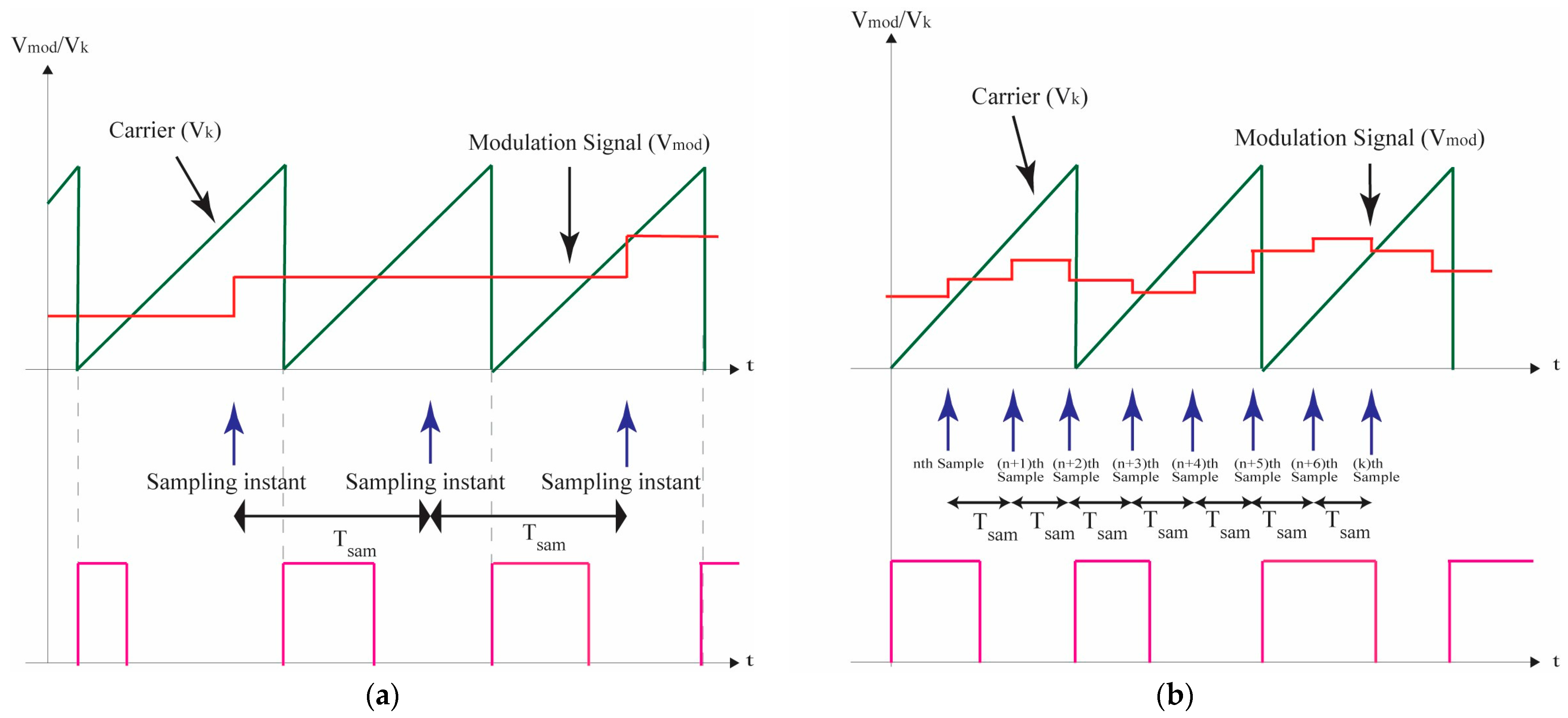
where ‘N’ stands for the number of samples per switching period. Therefore, for single sampling, f s a m p = f s w , and for multi-sampling, the control signal V m o d will have a sampling frequency f s a m p = N × f s w , and the subsequent ZOH time will be T s a m p = T s a m p = T s w N [13]. Modulation waveforms of single sampling and multi-sampling are shown in Figure 2.

3. Converter Topology and Modes of Operation

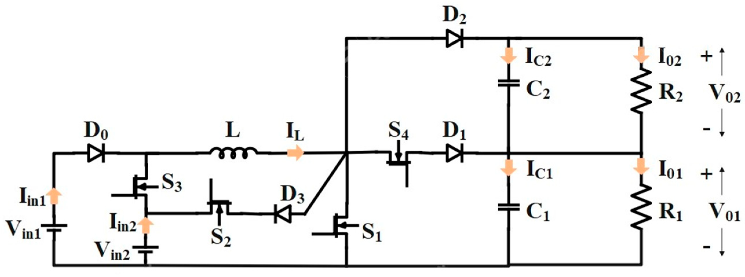
A shared-switch SI-MIMO converter is proposed in [7]. The input and output ports of the converter can be extended to any arbitrary numbers; however, in this work, two inputs and two output ports are used. A renewable energy source such as fuel cell stack can be used as the input voltage V i n 1 , while the input voltage source V i n 2 is a battery storage system, such that V i n 1 < V i n 2 . The converter supplies the output voltage V 01 to the electric traction motor of the EV at one voltage level and the output voltage V 02 to auxiliary services such as air conditioning, etc., at another voltage level. Furthermore, the battery V i n 2 can be discharged to the load in the battery discharging mode and when the load requirement is low, and the battery can be charged through the input voltage source V i n 1 in the battery charging mode, resulting in two modes of operation. The functionality of a converter with two inputs and two outputs is shown in Figure 3.
Among other SI-MIMO converter topologies, the selected topology has the advantage of a reduced number of switches. For N number of inputs and M number of outputs, the number of active switches required is (N + M − 1), which is less than most of the available topologies. However, this advantage also makes the converter highly vulnerable to poor transient performance. The topology of a shared-switch SI-MIMO converter is shown in Figure 4.
Detailed modeling of the converter in the battery discharging and charging modes is performed in the following sub-sections.

3.1. Modeling of Battery Discharging Mode

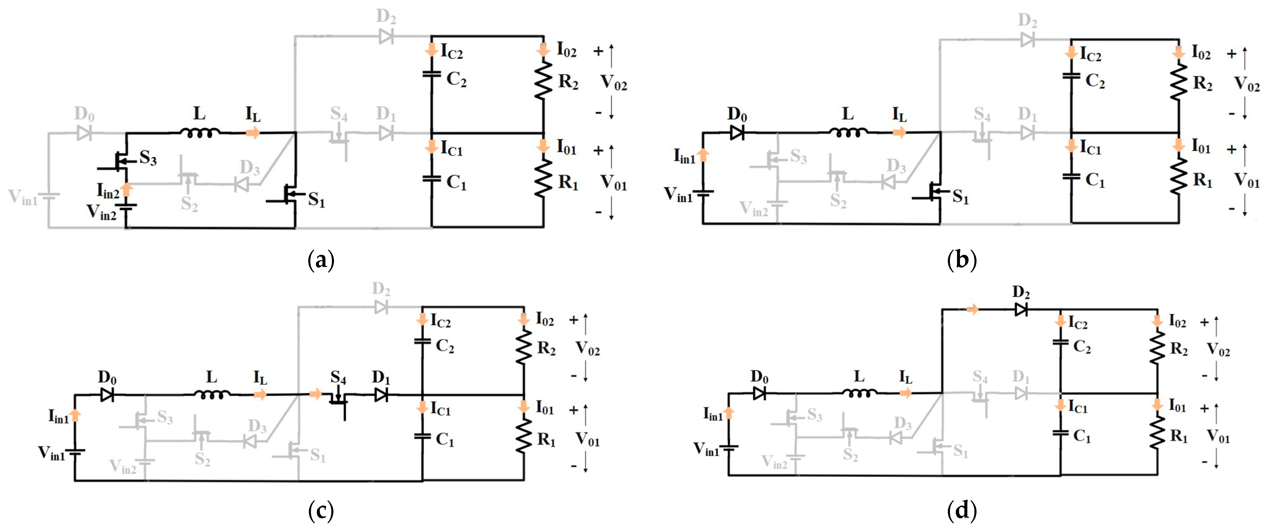
In the battery discharging mode, switch S 2 is permanently OFF, resulting in three effective switches being responsible for the operation. This mode is divided into four switching states, as shown in Figure 5.

3.1.1. Switching State 1

Switches S 1 and S 3 are ON during this state, while S 4 is OFF due to the reverse-biased diodes D 1 and D 2 . Since V i n 1 < V i n 2 , diode D o is also reverse-biased. The circuit of switching state 1 is shown in Figure 5a. During this state, the inductor is charged by V i n 2 , while the energy already stored in capacitors C 1 and C 2 is delivered to loads R 1 and R 2 .
The resulting inductor voltage and capacitor current equations are as follows:
{ L d i d t     = v i n 2                           C 1 d v 01 d t = v 01 R 1           C 2 d v 02 d t = v 02 R 2          

3.1.2. Switching State 2

Switch S 1 is ON while S 3 and S 4 are OFF during this state. The circuit of switching state 2 is shown in Figure 5b. During this state, the inductor is charged by V i n 1 , while the energy already stored in capacitors C 1 and C 2 is delivered to loads R 1 and R 2 .
The resulting inductor voltage and capacitor current equations are as follows:
{ L d i d t     = v i n 1           C 1 d v 01 d t = v 01 R 1 C 2 d v 02 d t = v 02 R 2

3.1.3. Switching State 3

Switches S 1 and S 3 are OFF while S 4 is ON during this state. The circuit of switching state 3 is shown in Figure 5c. During this state, the inductor is discharged to capacitors C 1 and load R 1 . C 1 is charged, while C 2 is discharged to R 2 .
The resulting inductor voltage and capacitor current equations are as follows:
{   L d i d t     = v i n 1 v 01 C 1 d v 01 d t = i L v 01 R 1     C 2 d v 02 d t = v 02 R 2            

3.1.4. Switching State 4

All switches are OFF during this state, and therefore diode D 2 becomes forward-biased. The circuit of switching state 4 is shown in Figure 5d. During this state, the inductor is discharged to capacitors C 1 and C 2 and loads R 1 and R 2 .
The resulting inductor voltage and capacitor current equations are as follows:
{ L d i d t     = v i n 1 ( v 01 + v 02 ) C 1 d v 01 d t = i L v 01 R 1                                     C 2 d v 02 d t = i L v 02 R 2                                    

3.2. Modeling of Battery Charging Mode

In the battery charging mode, switch S 3 is permanently OFF, resulting in three effective switches being responsible for the operation. This mode is divided into four switching states, as shown in Figure 6.

3.2.1. Switching State 1

Switch S 1 is ON, while switches S 2 and S 4 are OFF because of reverse bias. Diode D 2 is also reverse-biased in this state. The circuit of switching state 1 is shown in Figure 6a. During this state, the inductor is charged by V i n 1 , while the energy already stored in capacitors C 1 and C 2 is delivered to the loads R 1 and R 2 .
The resulting inductor voltage and capacitor current equations are as follows:
{ L d i d t     = v i n 1                           C 1 d v 01 d t = v 01 R 1           C 2 d v 02 d t = v 02 R 2          

3.2.2. Switching State 2

In this state, switch S 1 is turned OFF, while S 2 is ON. The circuit of switching state 2 is shown in Figure 6b. Diodes D 1 as well as D 2 are reverse-biased, which results in switch S 4 becoming OFF. During this state, the inductor delivers energy to battery V i n 2 , while the energy already stored in capacitors C 1 and C 2 is delivered to loads R 1 and R 2 .
The resulting inductor voltage and capacitor current equations are as follows:
{ L d i d t     = v i n 1 v i n 2   C 1 d v 01 d t = v 01 R 1                     C 2 d v 02 d t = v 02 R 2                    

3.2.3. Switching State 3

Switches S 1 and S 2 are OFF while S 4 is ON during this state. The circuit of switching state 3 is shown in Figure 6c. During this state, the inductor is discharged to capacitors C 1 and load R 1 . C 1 is charged, while C 2 is discharged to R 2 .
The resulting inductor voltage and capacitor current equations are as follows:
{ L d i d t     = v i n 1 v 01                   C 1 d v 01 d t = i L v 01 R 1                     C 2 d v 02 d t = v 02 R 2                            

3.2.4. Switching State 4

All switches are OFF during this state, and therefore diode D 2 becomes forward-biased. The circuit of switching state 4 is shown in Figure 6d. During this state, the inductor is discharged to capacitors C 1 and C 2 and loads R 1 and R 2 .
The resulting inductor voltage and capacitor current equations are as follows:
{ L d i d t     = v i n 1 ( v 01 + v 02 )                   C 1 d v 01 d t = i L v 01 R 1                                                   C 2 d v 02 d t = i L v 02 R 2                                                

3.3. Dynamic Model of the Converter

A state–space model is required to design the controller for the converter. Since the converter operates in two modes, i.e., the battery discharging and battery charging modes, each operational mode will require a different model.
An effective small-signal model can lead to proper closed-loop control development. The state variables in Equations (7)–(10) for the battery discharging mode and Equations (11)–(14) for the battery charging mode consist of DC terms (X) and perturbations ( x ^ ). Performing linearization of the above equations by using the Taylor series gives the following [7]:
{ v 01   = V 01 + v ^ 01 v 02   = V 02 + v ^ 02 i L   = I L + i ^ L     d 1   = D 1 + d ^ 1 d 2   = D 2 + d ^ 2 d 3   = D 3 + d ^ 3 d 4   = D 4 + d ^ 4
Substituting the above values in Equations (7)–(10), applying averaging, and neglecting second-order terms, we obtain the following small-signal equations for the battery discharging mode:
L d i ^ L t d t = ( V i n 2 V i n 1 ) d ^ 3 ( t ) + D 3 v ^ i n 2 + ( 1 D 3 ) v ^ i n 1 ( t )                                                                             ( 1 D 1 ) v ^ 01 ( t ) + ( D 4 1 ) v ^ 02 ( t ) + V 01 d ^ 1 ( t ) + V 02 d ^ 4 ( t )                   C 1 d v ^ 01 t d t = I L d ^ 1 t + 1 D 1 i ^ L t v ^ 01 R 1                                                                                                                               C 2 d v ^ 02 t d t = I L d ^ 4 t + 1 D 4 i ^ L t v ^ 02 R 2                                                                                                                            
Similarly, the small-signal equations for the battery charging mode can be obtained from Equations (11)–(14) and the Taylor series Equation (15) as follows:
L d i ^ L t d t = v ^ i n 1 t +   V i n 2 d ^ 1 t + ( D 1 D 2 ) v ^ i n 2 ( t ) + ( V 01 V i n 2 ) d ^ 2 t +             V 02 d ^ 4 t + D 2 1 v ^ 01 t 1 D 4 v ^ 02 t                                                         C 1 d v ^ 01 t d t = I L d ^ 2 t + 1 D 2 i ^ L t v ^ 01 R 1                                                                                                                               C 2 d v ^ 02 t d t = I L d ^ 4 t + 1 D 4 i ^ L t v ^ 02 R 2                                                                                                                            
In addition, the state model of the plant is given by Equation (18), through which the system can be represented in matrix form, where matrix X represents the state variables and Y represents the output matrix for both modes:
{ X ˙ = A X + B U   Y = C X + D U        
X = [ i ^ L ( t ) v ^ 01 ( t ) v ^ 02 ( t ) ] ,   Y = [ v ^ 01 ( t ) v ^ T ( t ) i ^ b ( t ) ]
Since during the battery discharging mode the active switches are S 1 , S 3 , and S 4 , while in battery charging mode the active switches are S 1 , S 2 , and S 4 , the input variables matrix U, consisting of duty cycles, will be different for both modes.
For the battery discharging mode, the matrix U is given as:
U = [ d ^ 4 ( t ) d ^ 1 ( t ) d ^ 2 ( t ) ]
And, for the battery charging mode, the matrix U is given as:
U = [ d ^ 4 ( t ) d ^ 3 ( t ) d ^ 1 ( t ) ]
The transfer function matrix is derived from the small-signal model using Equation (22):
G = Y ( s ) U ( s ) = C [ sI     A ] 1 B + D
The rank of the transfer function matrix is charactarized by the control variables. In this work, since the number of control variables is 3 in each mode, the rank of the transfer function matrices for both modes will be 3.
[ y 1 y 2 y 3 ] = [ g 11 g 12 g 13 g 21 g 22 g 23 g 31 g 32 g 33 ] [ u 1 u 2 u 3 ]
In the above equation, g i j represents the transfer function between output y i and input vector u j .
Therefore, the three transfer functions for the battery discharging mode are as follows:
g 11 = v ^ 01 ( s ) d ^ 4 s = V 02 1 D 1 L C 1 S + V 02 1 D 1 L R 2 C 1 C 2 1 D 1 D 4 1 I L L C 1 C 2 S 3 + R 1 C 1 + R 2 C 2 R 1 R 2 C 1 C 2 S 2 + L + 1 D 1 2 R 1 R 2 C 2 + D 4 1 2 R 1 R 2 C 1 L R 1 R 2 C 1 C 2 S + R 1 1 D 1 2 + D 4 1 2 R 2 L R 1 R 2 C 1 C 2
g 22 = v ^ T ( s ) d ^ 3 s = V i n 2 V i n 1 L 1 D 1 C 1 D 4 1 C 2 S + 1 D 1 R 2 C 1 C 2 ( D 4 1 ) R 1 C 1 C 2 V i n 2 V i n 1 L S 3 + R 1 C 1 + R 2 C 2 R 1 R 2 C 1 C 2 S 2 + L + 1 D 1 2 R 1 R 2 C 2 + D 4 1 2 R 1 R 2 C 1 L R 1 R 2 C 1 C 2 S + R 1 1 D 1 2 + D 4 1 2 R 2 L R 1 R 2 C 1 C 2
g 33 = i ^ b ( s ) d ^ 1 s = V 01 D 3 L S 2 + V 01 D 3 L 1 R 1 C 1 + 1 R 2 C 2 + 1 D 1 D 3 I L L C 1 S + V 01 D 3 L R 1 R 2 C 1 C 2 D 3 ( 1 D 1 ) I L L R 2 C 1 C 2 S 3 + R 1 C 1 + R 2 C 2 R 1 R 2 C 1 C 2 S 2 + L + D 2 1 2 R 1 R 2 C 2 + D 4 1 2 R 1 R 2 C 1 L R 1 R 2 C 1 C 2 S + R 1 D 2 1 2 + D 4 1 2 R 2 L R 1 R 2 C 1 C 2
And, the three transfer functions for the battery charging mode are given as:
g 11 = v ^ 01 ( s ) d ^ 4 s = V 02 1 D 2 L C 1 S + V 02 1 D 2 L R 2 C 1 C 2 1 D 2 D 4 1 I L L C 1 S 3 + R 1 C 1 + R 2 C 2 R 1 R 2 C 1 C 2 S 2 + L + D 2 1 2 R 1 R 2 C 2 + D 4 1 2 R 1 R 2 C 1 L R 1 R 2 C 1 C 2 S + R 1 D 2 1 2 + D 4 1 2 R 2 L R 1 R 2 C 1 C 2
    g 22 = v ^ T ( s ) d ^ 1 s = V i n 2 1 D 2 L C 1 + V i n 2 1 D 4 L C 2 S + V i n 2 1 D 2 L R 2 C 1 C 2 1 D 4 V i n 2 L R 1 C 1 C 2 S 3 + R 1 C 1 + R 2 C 2 R 1 R 2 C 1 C 2 S 2 + L + D 2 1 2 R 1 R 2 C 2 + D 4 1 2 R 1 R 2 C 1 L R 1 R 2 C 1 C 2 S + R 1 D 2 1 2 + D 4 1 2 R 2 L R 1 R 2 C 1 C 2
g 33 = i ^ b ( s ) d ^ 2 s = V i n 2 ) D 2 D 1 L S 2 + ( V 01 V i n 2 ) D 2 D 1 L 1 R 1 C 1 + 1 R 2 C 2 D 2 D 1 D 2 1 I L L C 1 S + ( V 01 V i n 2 ) D 2 D 1 L R 1 R 2 C 1 C 2 D 2 D 1 D 2 1 I L L R 2 C 1 C 2 + I L S 3 + R 1 C 1 + R 2 C 2 R 1 R 2 C 1 C 2 S 2 + L + D 2 1 2 R 1 R 2 C 2 + D 4 1 2 R 1 R 2 C 1 L R 1 R 2 C 1 C 2 S + R 1 D 2 1 2 + D 4 1 2 R 2 L R 1 R 2 C 1 C 2
The duty cycle values in both modes can be achieved from their respective steady-state equations [7]. For the battery discharging mode, the steady-state equations are expressed in Equation (30), while the technical parameters are given in Table 1 [7].
[ V 01 V i n 2 V i n 1 V 02 R 1 I b V 01 0 0 V 02 R 2 I b ] [ D 1 D 3 D 4 ] = [ V 02 + V 01 V i n 1 R 1 I b R 2 I b ]
Using the parameter values from Table 1 and Equation (30), the duty cycles can be calculated for the battery discharging mode, as shown in Table 2.
Similarly, for the battery charging mode, the steady-state equations are expressed in Equation (31), while the technical parameters are given in Table 3 [7].
[ V i n 2 V 01 V i n 2 V 02 V 01 V 01 + R 1 I b 0 V 02 V 02 R 2 I b ] [ D 1 D 2 D 4 ] = [ V 02 + V 01 V i n 1 R 1 I b R 2 I b ]
Using the parameter values from Table 3 and Equation (31), the duty cycles can be calculated for the battery charging mode, as shown in Table 4.

4. Proposed Advanced Multi-Sampling PWM Technique

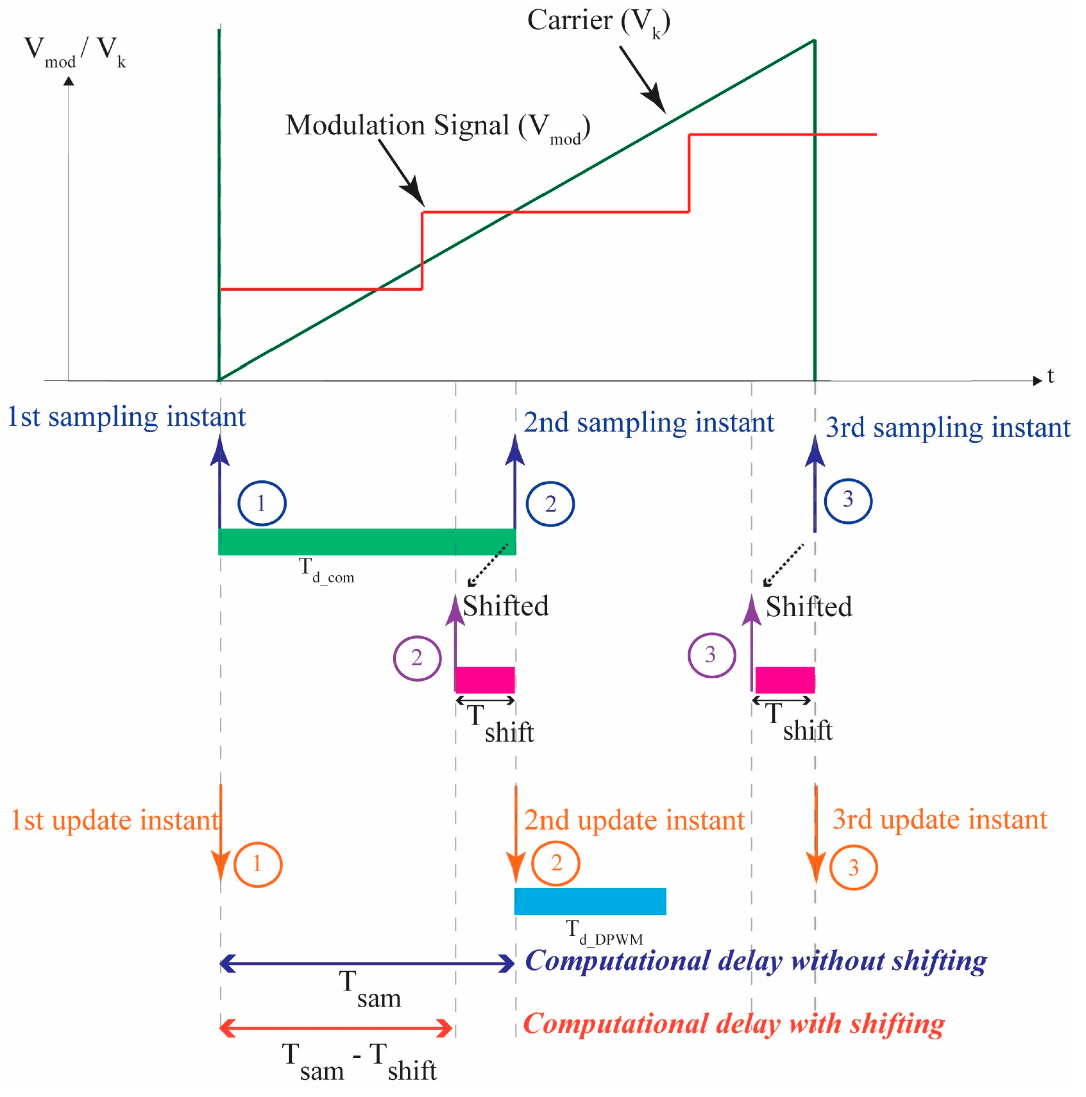
In contrast to the approach described in reference [21], which utilizes single sampling combined with sample shifting for DC-AC inverters, and reference [22], where both the PWM update instants and sampling instants are shifted in conjunction with multi-sampling, the proposed advanced multi-sampling PWM technique integrates multi-sampling solely with sample shifting within a specific control loop for the SI-MIMO DC-DC converter. The sampling instants are shifted towards the PWM update instants, effectively reducing the control delay by T s h i f t , as shown in Figure 7. The sampling instants (shown in blue) are shifted by a time of T s h i f t   (shown in the pink bar). Due to this shift, the effective time between samples and PWM update instants is also reduced by T s h i f t and, consequently, the computational delay ( T d _ c o m ) that was equal to one sampling cycle ( T s a m p ) before the sample shift is reduced to T s a m p   T s h i f t .
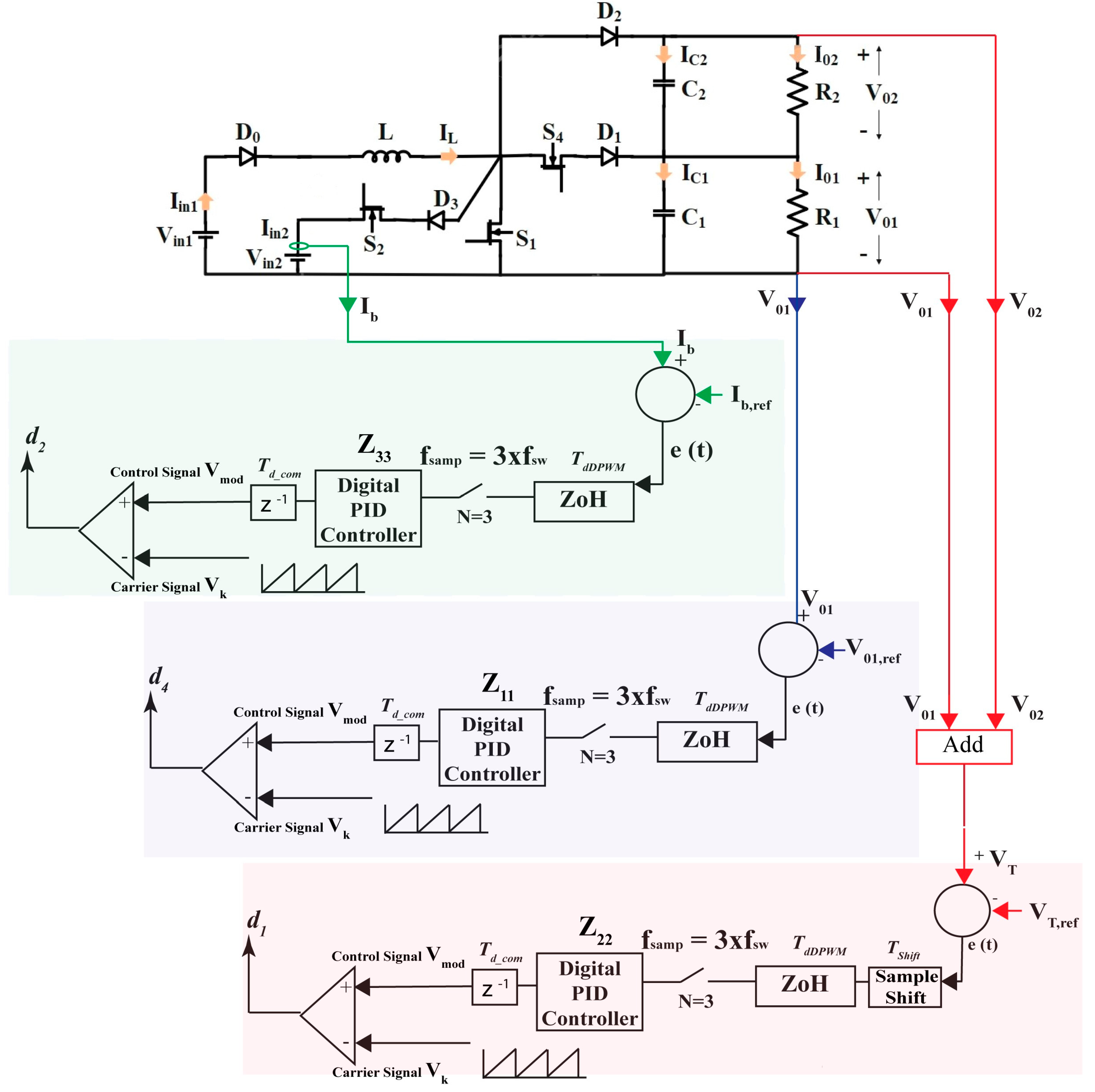
The implementation of the proposed method for the SI-MIMO converter during the battery discharging mode is shown in Figure 8. In this mode, switch S 2 of the converter is OFF throughout, as explained in Figure 5. S 1 governs the regulation of battery current I b to the desired value of I b , r e f . S 3 is responsible for regulating the total output voltage V T , which is equal to V 01 + V 02 , to the desired value of V T , r e f while S 4 regulates the output voltage V 01 to the desired value of V 01 , r e f . By regulating V T and V 01 , the output voltage V 02 is also regulated. Due to the presence of three active switches, three control loops are developed, and different PID controller transfer functions are obtained for each loop. For the regulation of the battery discharging current ( I b ), digital PID controller Z 33 is designed. This control loop employs multi-sampling with a sampling factor of 3 and provides a duty cycle d 1 to switch S 1 (top loop in the figure). For the regulation of output voltage V 01 , controller Z 11 is designed. This control loop also utilizes multi-sampling with a sampling factor of 3 and provides a duty cycle d 4 to switch S 4 (middle loop in the figure). Similarly, for the regulation of total output voltage VT, controller Z 22 is designed. The corresponding control loop provides a duty cycle d 3 to switch S 3 (bottom loop in the figure). In addition to multi-sampling, the sample shift is provided in this specific loop.
Similarly, the implementation of the proposed technique for the battery charging mode is shown in Figure 9. During this mode, switch S 3 of the converter is OFF throughout, as explained in Figure 6. S 2 governs the regulation of battery current I b to the desired value of I b , r e f . S 1 is responsible for regulating the total output voltage V T , which is equal to V 01 + V 02 , to the desired value of V T , r e f   , while S 4 regulates the output voltage V 01 to the desired value of V 01 , r e f . By regulating V T and V 01 , the output voltage V 02 is also regulated. Due to the presence of three active switches, three control loops are developed, and different PID controller transfer functions are obtained for each loop. For the regulation of the battery charging current ( I b ), digital PID controller Z 33 is designed. This control loop employs multi-sampling with a sampling factor of 3 and provides a duty cycle d 2 to switch S 2 (top loop in the figure). For the regulation of output voltage V 01 , controller Z 11 is designed. This control loop also utilizes multi-sampling with a sampling factor of 3 and provides a duty cycle d 4 to switch S 4 (middle loop in the figure). Similarly, for the regulation of total output voltage VT, the controller Z 22 is designed. The corresponding control loop provides a duty cycle d 1 to switch S 1 (bottom loop in the figure). In addition to multisampling, the sample shift is provided in this specific loop.

5. PID Controller Design

In this section, digital PID controllers are designed for the SI-MIMO DC-DC converter. For this purpose, PID controllers are first designed in a continuous-time domain and then discretized using the Tustin method.

5.1. PID Controller Design in Continuous-Time Domain

In the control design phase, PID controllers are implemented to regulate the system’s behavior based on previously derived transfer functions. Each PID controller is tailored to specific transfer functions, with its proportional, integral, and derivative gains adjusted. The PID controller for each transfer function G(s) is defined as:
C ( s ) = K p + K i s + K d ( s )
where K p ,   K i , and K d are the proportional, integral, and derivative gains, respectively. These gains were fine-tuned in the MATLAB tuner App (R2023a) (https://www.mathworks.com/products/matlab.html, accessed on 14 July 2024) to optimize the system performance, ensuring stability, responsiveness, and steady-state accuracy. The gains obtained after fine-tuning are shown in Table 5.
Similarly, for the battery charging mode, the gains obtained after fine-tuning are shown in Table 6.

5.2. Discretization

The Tustin method is used to convert continuous-time systems to discrete-time systems. It employs a first-order Pade approximation to achieve this conversion. Among the various discretization methods, the Tustin method is renowned for providing the most accurate representation of dynamic systems in the z-domain. This method involves shifting the poles and zeros of the continuous-time system across the z-plane using z = e s T s [31].
Using the Tustin Method, the continuous-time transfer function obtained can be discretized at a sampling time of T s =   4 × 10 5 s for single sampling and T s =   1.333 × 10 5 s for multi-sampling with a sampling factor of 3. The controller transfer functions C 11 , C 22 ,   and   C 33 for the battery discharging mode and battery charging mode are converted to discrete time transfer functions Z 11 ,   Z 22 ,   and   Z 33 , respectively, as shown in Table 7 and Table 8, respectively.

6. Simulation Setup

The proposed advanced multi-sampling PWM technique was validated in the non-linear MIMO system in MATLAB Simulink (R2023a) (https://www.mathworks.com/products/matlab.html, accessed on 14 July 2024).
The circuit model shown in Figure 4 was created in Simulink, with the parameters configured according to Table 1 [7] for the battery discharging mode and Table 3 [7] for the battery charging mode. Since each mode involves three active switches, separate digital PID controllers were designed to regulate each switch, as shown in Table 7 and Table 8. To demonstrate the effectiveness of the proposed method, the simulation setup included three cases—single sampling, multi-sampling, and the proposed method—that were conducted for each mode. To verify the dynamic performance of the converter, the following scenarios were tested:
(a)
A step change in the output reference voltage ( V 01 ) was introduced in both modes, changing the voltage from 80 V to 90 V. Results were recorded for all three cases in both modes.
(b)
Additionally, the converter’s performance for both modes was tested by changing the input voltage ( V i n 1 ) from 35 V to 25 V.
Case I (Single Sampling): For conventional single sampling, the sampling frequency is equal to the switching frequency. The control loop for single sampling is shown in Figure 10 where V o u t is a general representation of the output from any of the three loops of the converter, which could be V 01 , V T , or I b . Similarly, V r e f is a generalized representation of the desired output for any of the three loops, which could be V 0 1 , r e f , V T , r e f , or I b , r e f . The sample is fed to the digital PID controller, which generates a control/modulation signal V m o d depending upon the error. To realize the delayed PWM update method, the control signal is delayed by   0.5 T s a m . The total delay in the control loop becomes 1.5 T s a m . The delayed control signal is fed to the comparator, which is compared with a sawtooth carrier signal V k to generate the duty cycle.
In this paper, a switching frequency of 25 KHz was used; therefore, the sampling frequency was also 25 KHz, and the consequent sampling time becomes 1 25000 = 0.00004   s .
Case II (Multi-Sampling): To reduce delays in the control loops, a multi-sampling of factor 3 is used in all three loops. A generalized representation of the control loop is given in Figure 11. In this case, the sampling period T s a m = T s w N , where T s w is the switching period and N is the number of samples per switching period. By using 3 samples per switching period, the control loop delays are reduced by the same factor, resulting in a total control loop delay of 0.5 T s a m compared to 1.5 T s a m in case I.
Case III (Proposed/advanced multi-sampling PWM technique): In the proposed advanced multi-sampling PWM method, in addition to sampling each loop three times, the sampling in the control loop governing the total voltage ( V T ) is delayed by a small time, called the sample shift ( T s h i f t ) , of 1.5 × 10 6 s to shift the samples towards the PWM update instant slightly. The control loop is shown in Figure 12.
As shown in Table 9, for the given MIMO converter, in the case of the single-sampling method, the delay per loop is 1.5 T s w , which is reduced to 0.5 T s w by employing multi-sampling. Through the proposed method, total delay in the control loop governing total voltage ( V T ) is further reduced to 0.4625 T s w . The proposed method’s performance compared to the conventional single-sampling and multi-sampling methods is evaluated in the following section.

7. Results and Discussions

The simulation results for both modes of operation are expedited as follows.

7.1. Battery Discharging Mode

The transient responses of the MIMO DC converter under different conditions were analyzed and compared during the battery discharging mode. Firstly, when subjected to a step change in the output voltage V 01 , the converter’s performance was evaluated across three scenarios: single-sampling PWM, multi-sampling PWM, and the proposed method. The responses revealed distinct characteristics in each case, with the proposed method demonstrating superior transient behavior in terms of the settling time and overshoot. Furthermore, by subjecting the converter to a step change in the input voltage V i n 1 , additional insights into its dynamic response were gained. Again, the comparative analysis highlights the efficacy of the proposed technique in mitigating transient effects and enhancing the overall system stability. These findings underscore the effectiveness of the proposed approach in improving the transient response of MIMO DC converters, thereby contributing to advancements in power electronics control strategies.

7.1.1. Step Change in Output Voltage V 01

With a total simulation time of 7 s, the step change in the output voltage V 01 was introduced at 5 s. The reference output voltage was changed from 80 V to 90 V.
In the initial phase of our analysis, we examined the response of V 01 following a change in its reference voltage. Figure 13 depicts the outcomes of this investigation. Under the single-sampling PWM approach, the output voltage exhibited considerable ripple and demonstrated a sluggish settling time of 0.898 s. In contrast, employing the multi-sampling PWM strategy yielded a smoother, more stable waveform with a remarkably faster settling time of 0.124 s. Notably, the performance was further elevated when employing the proposed method. Here, the settling time was further reduced to an impressive 0.075 s, underscoring the efficacy of the proposed method in enhancing the transient response of the MIMO DC converter.
The transient response of V 02 resulting from a change in V 01 was analyzed. As illustrated in Figure 14, it is evident that the single-sampling PWM approach exhibited the most pronounced transient impact on V 02 following a change in V 01 , coupled with a settling time of 0.88 s. Conversely, employing the multi-sampling PWM method achieved a notably faster settling time of 0.15 s, which was accompanied by reduced ripple. Notably, with the implementation of our proposed method, the settling time was further enhanced to 0.1 s. Given the nature of an SI-MIMO converter, any alteration in one output is expected to affect the remaining outputs. However, our proposed method demonstrated minimal impact compared to the other two cases. Specifically, for the single-sampling approach, V 02 deviated by approximately 7 V, while the multi-sampling PWM method deviated by 3.53 V. Impressively, with our proposed method, V 02 underwent a minimal change of only 1.823 V, underscoring its effectiveness in mitigating the transient effects and enhancing the stability of the converter.
The transient performance of the three cases was further corroborated by comparing the inductor currents, as depicted in Figure 15. Observing the single-sampling scenario, it is evident that the settling time of the inductor current following a transient in V 01 was 0.861 s. In contrast, the multi-sampling approach achieved a notably faster settling time of 0.153 s. Notably, our proposed method showed the swiftest settling time of 0.071 s, underscoring its efficacy in enhancing the system’s transient response.
Similarly, the transient behavior of the battery discharging current in response to a change in V 01 was investigated. Consistent with the previous findings, Figure 16 highlights that the battery discharging current settled most rapidly when utilizing our proposed method. Specifically, the settling time for the battery current was 0.872 s for the single-sampling approach and 0.134 s for the multi-sampling method, and it was notably faster at 0.072 s for our proposed method. These quantitative values underscore the enhanced transient response achieved by the proposed method compared to alternative PWM control strategies, providing valuable insights into its efficacy in optimizing the system’s performance.
Table 10 shows a summary of the performance results for the three cases due to a change in V 01 .

7.1.2. Step Change in Output Voltage V i n 1

Following the analysis of converter performance in response to a change in the output voltage, simulations were conducted with a step change in the input voltage V i n 1 while keeping the reference output voltage of both outputs constant. Consistent with the previous simulation parameters, the step change was introduced at 5 s by changing the voltage of V i n 1 from 35 V to 25 V, and the performance of the three cases was analyzed.
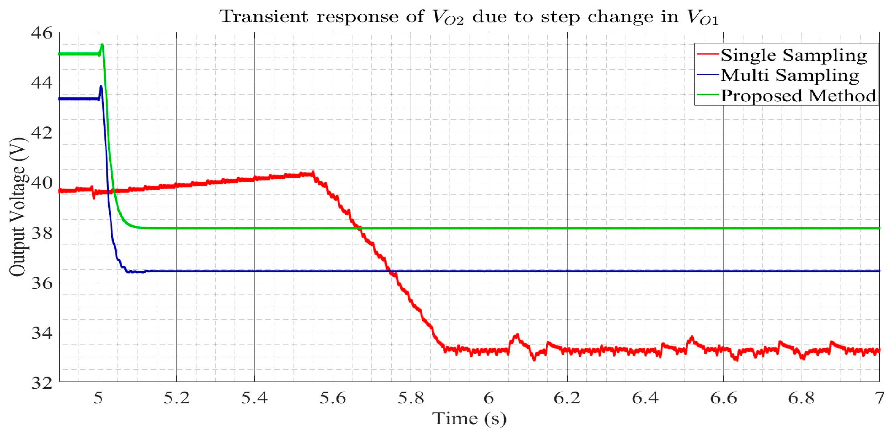
The response of V 01 for the three cases is depicted in Figure 17. In the conventional single-sampling scenario, the waveform displayed excessive ripples, which significantly complicated the precise analysis of the peak overshoot and undershoot. In contrast, both the multi-sampling and proposed methods presented clear representations of the overshoot and undershoot during the transient periods, accompanied by smooth steady-state conditions before and after the transient. Notably, during the transient phase, V 01 exhibited an overshoot of 1.5 V and an undershoot of 10.06 V in the multi-sampling case. However, with the proposed method, the overshoot was notably reduced to 0.06 V, although the undershoot increased to 12.4 V. These observations underscore the effectiveness of the proposed method in mitigating the overshoot, though with a slight increase in the undershoot, compared to the multi-sampling approach.
Similarly, V 02 was analyzed, and its response for the three cases is depicted in Figure 18. In the conventional single-sampling scenario, the waveform exhibited excessive ripples, significantly complicating the precise analysis of the peak overshoot and undershoot. This suggests that the single-sampling method may not be ideal for achieving precise control over V 02 during transient periods. In contrast, both the multi-sampling and proposed methods presented clear representations of the overshoot and undershoot during the transient periods, accompanied by smooth steady-state conditions before and after the transient. This indicates that both the multi-sampling and proposed methods offer improved transient response characteristics compared to single sampling, facilitating a more accurate output regulation of V 02 . Notably, during the transient phase, V 01 showed desirable response characteristics in both the multi-sampling and proposed methods by not experiencing excessive overshooting beyond the initial steady-state value. However, V 02 experienced an undershoot of 5.5 V in the case of multi-sampling and 6.8 V in the proposed method. This suggests that while both methods offer an improved transient response, there may still be some room for further optimization, particularly in minimizing the undershoot in V 02 . Nevertheless, the proposed method resulted in better output regulation compared to the multi-sampling approach, with a change of 5.79 V in V 02 after the transient compared to a change of 6.18 V in multi-sampling.
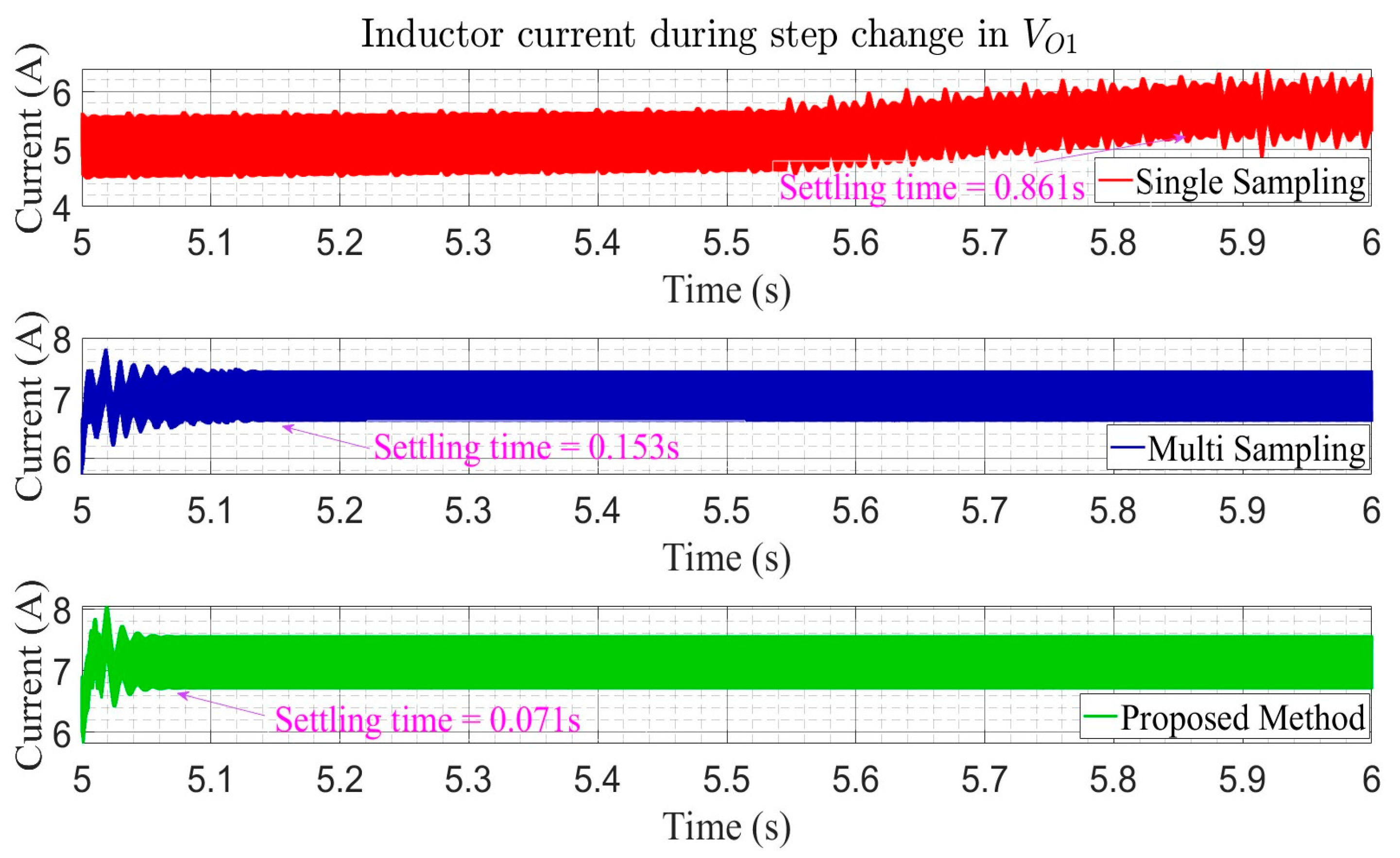
The transient performance of the three cases was further corroborated by comparing the inductor currents, as depicted in Figure 19. Observing the single-sampling scenario, it is evident that the settling time of the inductor current following a transient in V 01 was 0.86 s. In contrast, the multi-sampling approach achieved a notably faster settling time of 0.068 s. Notably, our proposed method exhibited the swiftest settling time of 0.063 s, underscoring its efficacy in enhancing the system’s transient response.
Table 11 shows a summary of the performance results for the three cases due to a change in V i n 1 .

7.2. Battery Charging Mode

The transient responses of the MIMO DC converter under different conditions were analyzed and compared during the battery charging mode. Firstly, when subjected to a step change in the output voltage V 01 , the converter’s performance was evaluated across three scenarios: single-sampling PWM, multi-sampling PWM, and the proposed method. The responses revealed distinct characteristics in each case, with the proposed method demonstrating superior transient behavior in terms of the settling time and overshoot. Furthermore, by subjecting the converter to a step change in the input voltage ( V i n 1 ), additional insights into its dynamic response were gained. Again, the comparative analysis highlights the efficacy of the proposed technique in mitigating transient effects and enhancing the overall system stability. These findings underscore the effectiveness of the proposed approach in improving the transient response of MIMO DC converters, thereby contributing to advancements in power electronics control strategies.

7.2.1. Step Change in Output Voltage V 01

With a total simulation time of 5 s, a step change in the output voltage V 01 was introduced at 2.5 s. The reference output voltage was changed from 80 V to 90 V.
The response of V 01 was examined following a change in its reference voltage. Figure 20 depicts the response of V 01 under the effect of a reference change. In the single-sampling PWM approach, the output voltage exhibited a response time of 0.0362 s and settling time of 0.2886 s. Both the response and settling time were reduced to 0.0099 s and 0.152 s by using the multi-sampling PWM method. By using the proposed method, with a slight trade-off in terms of the response time (0.01 s), the settling time was further reduced to 0.147 s, as shown in Figure 20. While the proposed method showed superior transient performance among all three cases, the single-sampling approach excelled in voltage regulation both before and after the introduction of the transient. Specifically, the deviation from the reference voltage in the single-sampling case was measured at 0.72 V before the transient and 2.46 V after the transient. In contrast, the deviation from the reference voltage in both the multi-sampling and proposed methods was 2.79 V before the transient and 6.56 V after the transient.
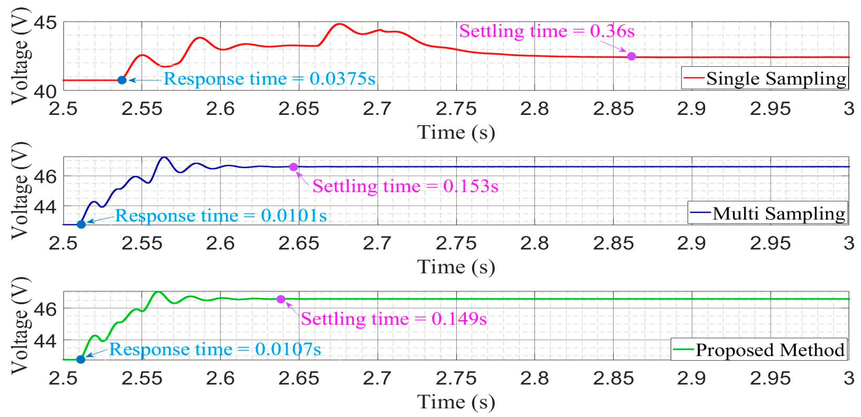
After analyzing V 01 , the transient response of V 02 resulting from a change in V 01 was examined. As illustrated in Figure 21, the single-sampling approach exhibited the longest response time and settling time, measured at 0.0375 s and 0.36 s, respectively. In contrast, the multi-sampling approach demonstrated a response time of 0.0101 s and a settling time of 0.153 s. With the proposed method, the settling time was further reduced to 0.149 s, though with a slightly higher response time of 0.0107 s, as depicted in Figure 21. While the proposed method exhibited superior transient performance among all three cases, the single-sampling approach excelled in terms of voltage regulation both before and after the introduction of the transient. Specifically, the deviation from the reference voltage in the single-sampling case was measured at 1.32 V before the transient and 0.8 V after the transient. In contrast, the deviation from the reference voltage in both the multi-sampling and proposed method was 1.85 V before the transient and 5.14 V after the transient.
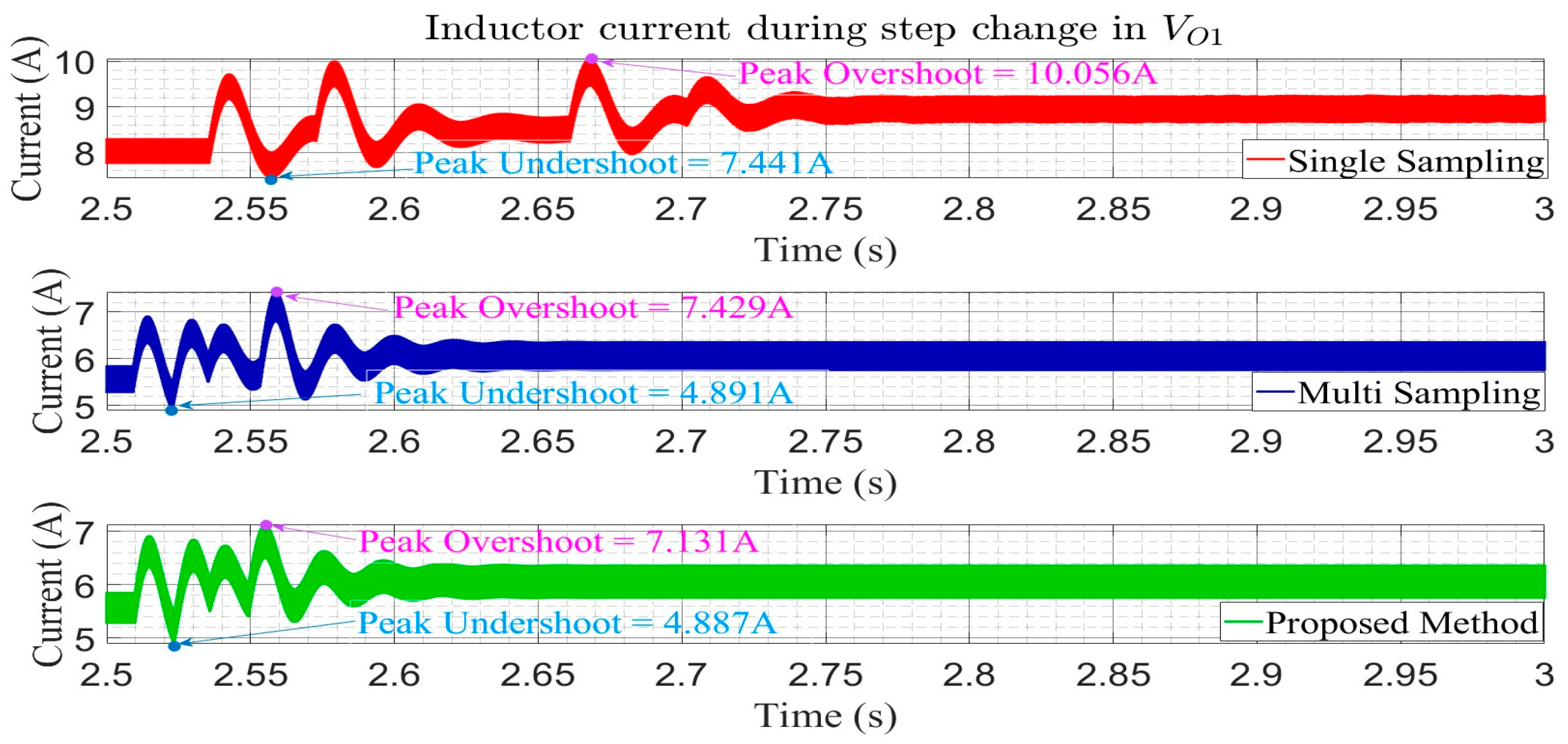
The inductor current during a step change in V 01 is depicted in Figure 22 for the three cases. The inductor current in the single-sampling approach demonstrated the largest overshoot and undershoot among the three cases, and the proposed method had the lowest overshoot and undershoot.
The battery charging current during a step change in V 01 is shown in Figure 23. The settling time of the battery current after the transient was 0.294 s for single sampling, which was reduced to 0.175 s with multi-sampling. The proposed method resulted in a faster settling time of 0.171 s.
A summary of the results of the transient performance of the converter during a step change in V 01 during the battery charging mode is given in Table 12.

7.2.2. Step Change in Input Voltage V in 1

Following the analysis of the converter performance in response to a change in the output voltage, simulations were conducted with a step change in the input voltage V i n 1 while keeping the reference output voltage of both outputs constant. Consistent with the previous simulation parameters, a step change was introduced at 2.5 s by changing the voltage of V i n 1 from 35 V to 25 V, and the performance of the three cases was analyzed.
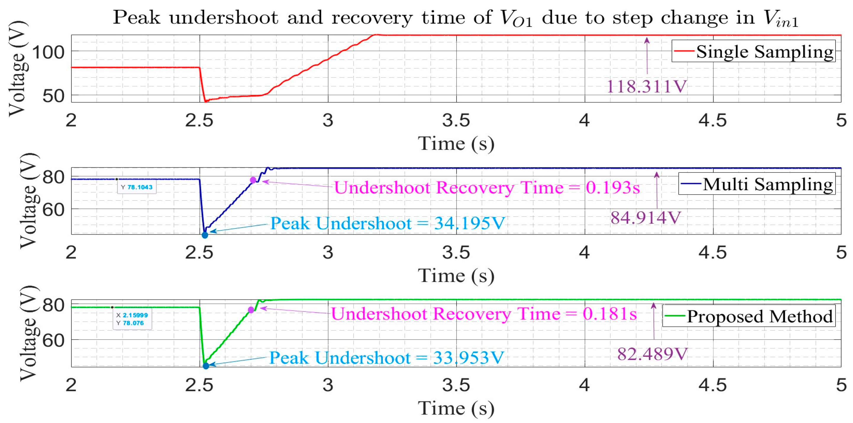
The response of V 01 for the three cases is depicted in Figure 24. In the conventional single-sampling scenario, V 01 failed to track the reference and reached 118.311 V instead of 80 V. In the case of multi-sampling, V 01 went through an undershoot of 34.185 V before reaching a steady-state value of 84.914 V, with an undershoot recovery time of 0.193 s. The proposed method improved the undershoot (33.953 V) and recovery time (0.181 s) as well as the voltage regulation (82.489 V).
V 02 showed similar behavior following the transient in V i n 1 . In the single-sampling approach, V 02 failed to track the reference and went to almost 0 V. In the case of multi-sampling, V 02 went through an undershoot of 19.53 V before reaching a steady-state value of 42.56 V, with an undershoot recovery time of 0.190 s. The proposed method improved the undershoot (19.49 V), recovery time (0.177 s), and voltage regulation (41.38 V), as shown in Figure 25.
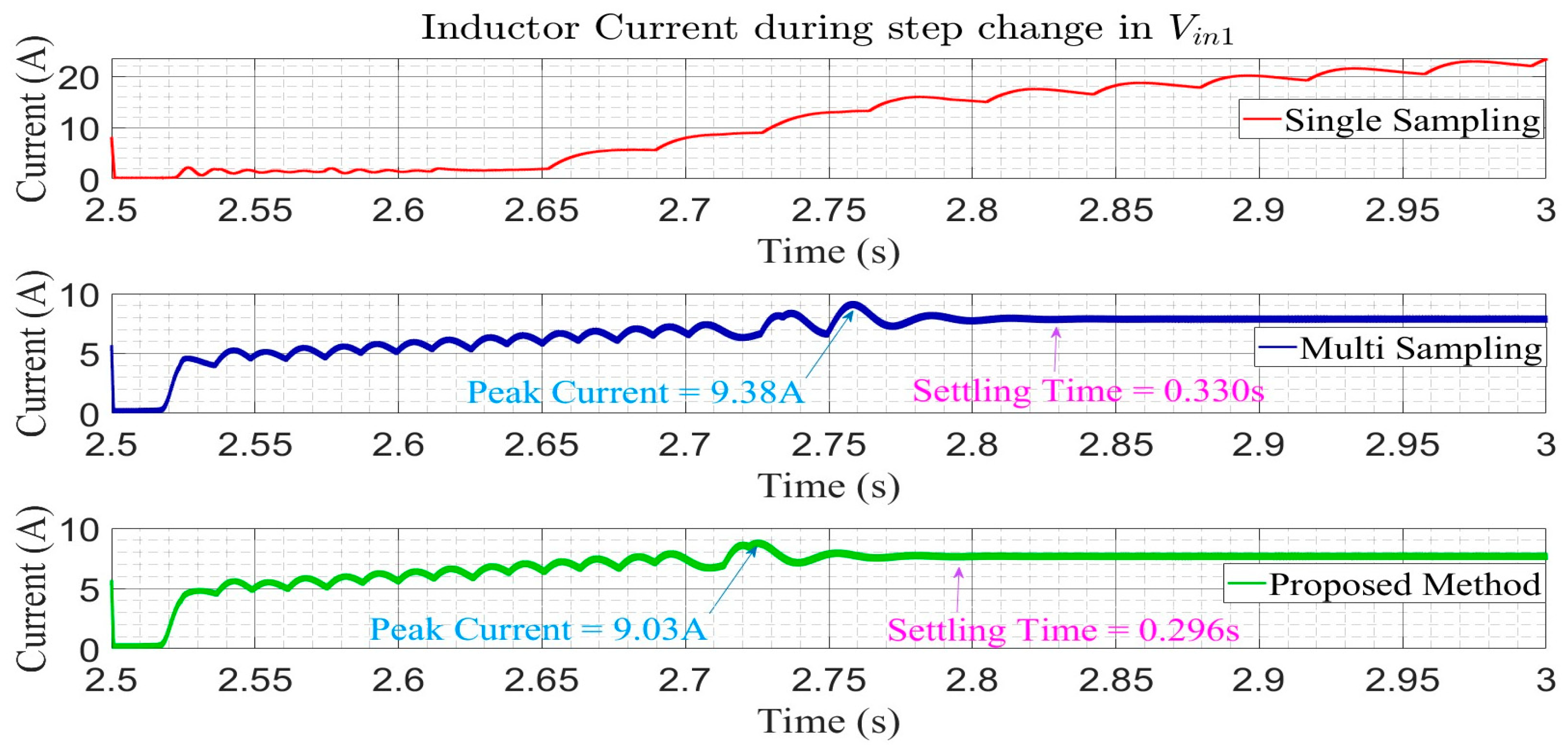
The inductor current during the step change in V i n 1 reached a high value of 28.8 A in 3.2 s, which corresponds with the previous results, where V 01 reached an abnormally high voltage and V 02 dropped to near 0 V. In the case of multi-sampling, the inductor current reached a peak value of 9.38 A and a settling time of 0.33 s. The proposed method reduced the peak inductor current overshoot to 9.03 A and settling time to 0.296 s, as depicted in Figure 26.
A summary of the results obtained during the step change in V i n 1 are shown in Table 13.
Although control delays are inherent in digital control, these delays are seldom considered when designing digital control for SI-MIMO DC-DC converters. Most previous works on control delays and their mitigation techniques have been performed in SISO topologies. Table 14 shows a comparison of the proposed method with previous works on the digital control of SI-MIMO converters.
In real-world applications such as EVs, a MIMO converter can play a crucial role in enhancing performance. EVs require different voltage levels for various applications; for instance, the voltage needed for the electric traction motor differs from that required for auxiliary services like air conditioning and lighting. Additionally, to optimize their running performance and increase their range, EVs often integrate multiple power sources such as fuel cells alongside battery storage systems, making MIMO converters an ideal choice for implementation.
Moreover, EVs are dynamic systems characterized by frequent changes in acceleration, braking, and battery charging/discharging. These dynamics necessitate rapid adjustments in voltage levels both at the inputs (e.g., during battery charging/discharging) and outputs (e.g., when adjusting the motor speed), without significant voltage overshoot or undershoot. The proposed method implemented on the SI-MIMO converter enhanced the dynamic performance by effectively managing these voltage changes by improving the response and settling time without introducing significant overshoot/undershoot.
The simulations performed in this paper replicate real-world EV scenarios. For instance, the input voltage V i n 1 manages tasks like battery charging and supplying the load. As the fuel cell charges the battery and provides power to the load, its voltage naturally declines—a scenario simulated with a step change from 35 V to 25 V. Similarly, the voltage delivered to the electric traction motor fluctuates with the vehicle speed, necessitating higher voltage levels during acceleration. This simulation incorporated a step change in the output voltage reference from 80 V to 90 V to model acceleration dynamics. The proposed method can be practically implemented using DSPs/microprocessors with the existing parameters defined in Table 1 and Table 3.

8. Conclusions

In this paper, an advanced multi-sampling PWM method was proposed for a shared-switch SI-MIMO DC-DC converter. By implementing multi-sampling in all control loops of the converter and additionally introducing a small shift in the samples of the control loop governing the total output voltage, the transient performance of the shared-switch SI-MIMO converter was substantially improved. The efficacy of the proposed method was validated by performing simulations under various scenarios (providing a step change in the output reference voltage and a step change in the input voltage). The proposed method was compared with conventional single- and multi-sampling approaches. During the battery discharging mode, a step transient in the output reference was introduced, and the output reference voltage was changed from 80 V to 90 V, and in order to measure the performance during variations in the input voltage, a step change in the input was introduced and the input voltage was changed from 35 V to 25 V. Utilizing the proposed method, the output voltage achieved a settling time of 0.075 s in response to the step change in its reference, significantly outperforming multi-sampling, which yielded settling time of 0.124 s, and single sampling, which exhibited an even longer settling time of 0.898 s. It also demonstrated a minimal overshoot of 0.06 volts compared to 1.5 volts with multi-sampling during the step change in the input voltage. Similarly, in the battery charging mode, upon a step change in the reference output voltage, the proposed method effectively minimized the overshoot of the output voltage to 0.845 volts compared to 1.175 volts with multi-sampling and decreased the inductor current settling time to 0.296 s from 0.330 s recorded under multi-sampling. These results show that the proposed method significantly enhanced the transient performance of the shared-switch SI-MIMO converter compared to conventional single- and multi-sampling methods, making the method suitable for highly dynamic systems like EVs.
While the proposed method involves multi-sampling integrated with sample shifting in a specific loop, future research could focus on further refining and exploring hybrid strategies that combine the strengths of single- and multi-sampling PWM approaches. Additionally, the method was implemented on a shared-switch SI-MIMO converter topology, providing valuable insights into the transient performance improvement in such a configuration, and future works may include testing and validating the effectiveness of the proposed method on other DC converter topologies. Furthermore, by incorporating the non-ideal characteristics of active components such as switch turn-on resistance r d s , diode internal resistance r d , diode forward-voltage drop v d , etc., into the converter model, a more realistic analysis and more accurate results can be obtained.

Author Contributions

Conceptualization and supervision, K.H.; methodology, software, validation, formal analysis, investigation, and writing—original draft preparation, H.S.; writing—review and editing and funding acquisition, M.S. and A.S.; project administration, S.M. and L.K. All authors have read and agreed to the published version of the manuscript.

Funding

This research received no external funding.

Data Availability Statement

The original contributions presented in the study are included in the article, further inquiries can be directed to the corresponding author.

Conflicts of Interest

The authors declare no conflicts of interest.

References

  1. Behjati, H.; Davoudi, A. A Multiple-Input Multiple-Output DC–DC Converter. IEEE Trans. Ind. Appl. 2013, 49, 3. [Google Scholar] [CrossRef]
  2. Rehman, Z.; Al-Bahadly, I.; Mukhopadhyay, S. Dual input-dual output single inductor dc-dc converter. In Proceedings of the IECON 2015-41st Annual Conference of the IEEE Industrial Electronics Society, Yokohama, Japan, 9–12 November 2015; pp. 004848–004853. [Google Scholar] [CrossRef]
  3. Prajof, P.; Agarwal, V. Novel solar PV-fuel cell fed dual-inputdual-output dc-dc converter for dc microgrid applications. In Proceedings of the 2015 IEEE 42nd Photovoltaic Specialist Conference (PVSC), New Orleans, LA, USA, 14–19 June 2015; pp. 1–6. [Google Scholar] [CrossRef]
  4. Shao, H.; Li, X.; Tsui, C.-Y.; Ki, W.-H. A Novel Single-Inductor Dual-Input Dual-Output DC–DC Converter with PWM Control for Solar Energy Harvesting System. IEEE Trans. Very Large Scale Integr. (VLSI) Syst. 2014, 22, 1693–1704. [Google Scholar] [CrossRef]
  5. Babaei, E.; Abbasi, O. Structure for multi-input multioutput dc–dc boost converter. IET Power Electron. 2016, 9, 9–19. [Google Scholar] [CrossRef]
  6. Saeed, L.; Khan, M.Y.A.; Arif, M.; Majid, A.; Saleem, J. A multiple-input multiple-output non-inverting non-isolated bidirectional buck/boost converter for storage application. In Proceedings of the 2018 International Conference on Computing, Mathematics and Engineering Technologies (iCoMET), Sukkur, Pakistan, 3–4 March 2018; pp. 1–6. [Google Scholar]
  7. Nahavandi, A.; Hagh, M.T.; Sharifian MB, B.; Danyali, S. A nonisolated multiinput multioutput DC–DC boost converter for electric vehicle applications. IEEE Trans. Power Electron. 2014, 30, 1818–1835. [Google Scholar] [CrossRef]
  8. Li, X.L.; Dong, Z.; Tse, C.K.; Lu, D.D.-C. Single-Inductor Multi-Input Multi-Output DC–DC Converter with High Flexibility and Simple Control. IEEE Trans. Power Electron. 2020, 35, 13104–13114. [Google Scholar] [CrossRef]
  9. Dong, Z.; Li, Z.; Li, X.L.; Tse, C.K.; Zhang, Z. Single-Inductor Multiple-Input Multiple-Output Converter with Common Ground, High Scalability, and No Cross-Regulation. IEEE Trans. Power Electron. 2021, 36, 6750–6760. [Google Scholar] [CrossRef]
  10. Abu Qahouq, J.; Arikatla, V.; Arunachalam, T. Modified Digital Pulse Width Modulator for Power Converters with a Reduced Modulation Delay. J. Power Electron. 2012, 12, 98–103. [Google Scholar] [CrossRef]
  11. Chang, J.-S.; Oh, H.-S.; Jun, Y.-H.; Kong, B.-S. Fast Output Voltage-Regulated PWM Buck Converter with an Adaptive Ramp Amplitude Control. IEEE Trans. Circuits Syst. II Express Briefs 2013, 60, 712–716. [Google Scholar] [CrossRef]
  12. Suh, J.-D.; Seok, J.; Kong, B.-S. A Fast Response PWM Buck Converter with Active Ramp Tracking Control in a Load Transient Period. IEEE Trans. Circuits Syst. II Express Briefs 2019, 66, 467–471. [Google Scholar] [CrossRef]
  13. Trejos, A.; Goez, M.; Ramos-Paja, C.A.; Arango, E. Digital controllers design analysis for DC/DC converters in PV applications. In Proceedings of the 2013 4th IEEE International Symposium on Power Electronics for Distributed Generation Systems (PEDG), Rogers, AR, USA, 8–11 July 2013; pp. 1–6. [Google Scholar] [CrossRef]
  14. Moon, S.; Choe, J.-M.; Cho, Y.; Lai, J.-S. Priority based current control design in high speed sensorless PMSM drives. In Proceedings of the 9th International Conference on Power Electronics and ECCE Asia (ICPE-ECCE Asia), Seoul, Republic of Korea, 26 February–1 March 2015; pp. 2129–2134. [Google Scholar]
  15. Kuo, C.-C.; Tzou, Y.-Y. FPGA predictive control for single-phase active NPC grid inverters with multi-sampling technique. In Proceedings of the IECON 2016—42nd Annual Conference of the IEEE Industrial Electronics Society, Florence, Italy, 24–27 October 2016; pp. 2295–2300. [Google Scholar]
  16. Chen, Y.; Xie, F.; Zhang, B.; Qiu, D.; Xu, M. Analysis of Digital PCM-Controlled Boost Converter with Trailing-Edge Modulation Based on z-Domain and Describing-Function Model. IEEE J. Emerg. Sel. Top. Power Electron. 2020, 8, 3250–3259. [Google Scholar] [CrossRef]
  17. Enslin, J.; Heskes, P. Harmonic Interaction Between a Large Number of Distributed Power Inverters and the Distribution Network. IEEE Trans. Power Electron. 2004, 19, 1586–1593. [Google Scholar] [CrossRef]
  18. He, S.; Zhou, D.; Wang, X.; Blaabjerg, F. Overview of Multisampling Techniques in Power Electronics Converters. In Proceedings of the IECON 2019—45th Annual Conference of the IEEE Industrial Electronics Society, Lisbon, Portugal, 14–17 October 2019; pp. 1922–1927. [Google Scholar]
  19. Corradini, L.; Mattavelli, P. Analysis of Multiple Sampling Technique for Digitally Controlled dc-dc Converters. In Proceedings of the 37th IEEE Power Electronics Specialists Conference, Jeju, Republic of Korea, 18–22 June 2006; pp. 1–6. [Google Scholar] [CrossRef]
  20. Yang, L.; Chen, Y.; Luo, A.; Huai, K.; Zhou, L.; Zhou, X.; Wu, W.; Tan, W.; Xie, Z. A Double Update PWM Method to Improve Robustness for the Deadbeat Current Controller in Three-Phase Grid-Connected System. J. Electr. Comput. Eng. 2018, 1–13. [Google Scholar] [CrossRef]
  21. Mattavelli, P.; Polo, F.; Sattin, S.; Lago, F.D. Dynamic improvement in UPS by means of control delay minimization. In Proceedings of the Conference Record of the 2004 IEEE Industry Applications Conference, 2004, 39th IAS Annual Meeting, Seattle, WA, USA, 3–7 October 2004; Volume 2, pp. 843–849. [Google Scholar]
  22. He, S.; Zhou, D.; Wang, X.; Zhao, Z.; Blaabjerg, F. A Review of Multisampling Techniques in Power Electronics Applications. IEEE Trans. Power Electron. 2022, 37, 10514–10533. [Google Scholar] [CrossRef]
  23. Wang, B.; Zhang, X.; Ye, J.; Gooi, H.B. Deadbeat Control for a Single-Inductor Multiple-Input Multiple-Output DC–DC Converter. IEEE Trans. Power Electron. 2019, 34, 1914–1924. [Google Scholar] [CrossRef]
  24. Wang, B.; Xian, L.; Kanamarlapudi, V.R.K.; Tseng, K.J.; Ukil, A.; Gooi, H.B. A Digital Method of Power-Sharing and Cross-Regulation Suppression for Single-Inductor Multiple-Input Multiple-Output DC–DC Converter. IEEE Trans. Ind. Electron. 2017, 64, 2836–2847. [Google Scholar] [CrossRef]
  25. Shen, Z.; Chang, X.; Wang, W.; Tan, X.; Yan, N.; Min, H. Predictive Digital Current Control of Single-Inductor Multiple-Output Converters in CCM with Low Cross Regulation. IEEE Trans. Power Electron. 2012, 27, 1917–1925. [Google Scholar] [CrossRef]
  26. Parayandeh, A.; Stupar, A.; Prodić, A. Programmable digital controller for multi-output DC-DC converters with a time-shared inductor. In Proceedings of the 2006 37th IEEE Power Electronics Specialists Conference, Jeju, Republic of Korea, 18–22 June 2006; pp. 1–6. [Google Scholar]
  27. Trevisan, D.; Mattavelli, P.; Tenti, P. Digital Control of Single-Inductor Multiple-Output Step-Down DC–DC Converters in CCM. IEEE Trans. Ind. Electron. 2008, 55, 3476–3483. [Google Scholar] [CrossRef]
  28. Yang, D.; Ruan, X.; Wu, H. A Real-Time Computation Method with Dual Sampling Mode to Improve the Current Control Performance of the LCL-Type Grid-Connected Inverter. IEEE Trans. Ind. Electron. 2015, 62, 4563–4572. [Google Scholar] [CrossRef]
  29. Van de Sype, D.M.; De Gusseme, K.; Van den Bossche, A.P.; Melkebeek, J.A. Small-signal Laplace-domain analysis of uniformly-sampled pulse-width modulators. In Proceedings of the 2004 IEEE 35th Annual Power Electronics Specialists Conference (IEEE Cat. No.04CH37551), Aachen, Germany, 20–25 June 2004; Volume 6, pp. 4292–4298. [Google Scholar] [CrossRef]
  30. Pan, D.; Ruan, X.; Bao, C.; Li, W.; Wang, X. Capacitor-Current-Feedback Active Damping with Reduced Computation Delay for Improving Robustness of LCL-Type Grid-Connected Inverter. IEEE Trans. Power Electron. 2014, 29, 3414–3427. [Google Scholar] [CrossRef]
  31. Yanarateş, C.; Okur, S.; Altan, A. Performance analysis of digitally controlled nonlinear systems considering time delay issues. Heliyon 2023, 9, e20994. [Google Scholar] [CrossRef] [PubMed]
Figure 1. Overview of control delays.
Energies 17 03633 g001
Figure 2. Modulation waveforms: (a) single sampling; (b) multi−sampling.
Energies 17 03633 g002
Figure 3. Block diagram of SI−MIMO converter.
Energies 17 03633 g003
Figure 4. Topology of shared−switch SI−MIMO converter.
Energies 17 03633 g004
Figure 5. Switching states in battery discharging mode: (a) switching state 1; (b) switching state 2; (c) switching state 3; (d) switching state 4.
Energies 17 03633 g005
Figure 6. Switching states in battery charging mode: (a) switching state 1; (b) switching state 2; (c) switching state 3; (d) switching state 4.
Energies 17 03633 g006
Figure 7. Proposed advanced multi−sampling PWM technique.
Energies 17 03633 g007
Figure 8. Advanced multi−sampling PWM technique in battery discharging mode.
Energies 17 03633 g008
Figure 9. Advanced multi−sampling PWM technique in battery charging mode.
Energies 17 03633 g009
Figure 10. Block diagram of single−sampling PWM control.
Energies 17 03633 g010
Figure 11. Block diagram of multi−sampling PWM control.
Energies 17 03633 g011
Figure 12. Block diagram of proposed advanced multi−sampling PWM technique.
Energies 17 03633 g012
Figure 13. Individual transient response waveforms of three cases.
Energies 17 03633 g013
Figure 14. Response of V 02 due to change in V 01 .
Energies 17 03633 g014
Figure 15. Transient response of inductor current.
Energies 17 03633 g015
Figure 16. Transient response of battery discharging current.
Energies 17 03633 g016
Figure 17. Response of V 01 in three cases.
Energies 17 03633 g017
Figure 18. Response of V 02   in three cases.
Energies 17 03633 g018
Figure 19. Inductor current during step change in V i n 1 .
Energies 17 03633 g019
Figure 20. Response of V 01 in three cases due to step change in reference.
Energies 17 03633 g020
Figure 21. Response of V 02 in three cases due to change in V 01 .
Energies 17 03633 g021
Figure 22. Transient response of inductor current.
Energies 17 03633 g022
Figure 23. Transient response of battery charging current.
Energies 17 03633 g023
Figure 24. Transient response of V 01 after step change in V i n 1 .
Energies 17 03633 g024
Figure 25. Transient response of V 02 after step change in V i n 1 .
Energies 17 03633 g025
Figure 26. Inductor current during step change in V i n 1 .
Energies 17 03633 g026
Table 1. Technical specifications of SI-MIMO converter during battery discharging mode.
ParametersSymbolValue
Input voltage 1 V i n 1 35 V
Input voltage 2 V i n 2 48 V
Output voltage 1 V 01 80 V
Output voltage 2 V 02 40 V
Battery discharging current I b 3 A
Resistance 1 R 1 35 Ω
Resistance 2 R 2 35 Ω
Capacitor 1 C 1 0.00047 F
Capacitor 2 C 2 0.00047 F
InductorL0.0013 H
Switching frequencyfs25 KHz
Table 2. Duty cycle values for battery discharging mode.
Duty CycleValue
D 1 0.578
D 3 0.554
D 4 0.789
Table 3. Technical specifications of SI-MIMO converter during charging mode.
ParametersSymbolValue
Input voltage 1 V i n 1 35 V
Input voltage 2 V i n 2 48 V
Output voltage 1 V 01 80 V
Output voltage 2 V 02 40 V
Battery charging current I b −0.9 A
Resistance 1 R 1 70 Ω
Resistance 2 R 2 70 Ω
Capacitor 1 C 1 0.00047 F
Capacitor 2 C 2 0.00047 F
InductorL0.0013 H
Switching frequencyfs25 KHz
Table 4. Duty cycle values for battery charging mode.
Duty CycleValue
D 1 0.88
D 2 0.437
D 4 0.719
Table 5. K p , K i , and K d gains for controller transfer functions in battery discharging mode.
PID Gains C 11 C 22 C 33
K p 7.7750.0038670.07106
K i 1.38 × 1040.4138.35
K d 0.0010958.884 × 10−60
Table 6. K p , K i , and K d gains for controller transfer functions in battery charging mode.
PID Gains C 11 C 22 C 33
K p 0.110700
K i 36.760.1748−1.424
K d 8.332 × 10−500
Table 7. Discretization of controller transfer function in battery discharging mode.
Single SamplingMulti-SamplingProposed Method
Z 11 62.8 z 2 108.9 z + 47.25 z 2 1 172.1 z 2 328.3 z + 156.6 z 2 1 172.1 z 2 328.3 z + 156.6 z 2 1
Z 22 0.4481 z 2 0.8884 z + 0.4403 z 2 1 1.336 z 2 2.665 z + 1.329 z 2 1 1.336 z 2 2.665 z + 1.329 z 2 1
Z 33 0.07183 z 0.07029 z 1 0.07132 z 0.0708 z 1 0.07132 z 0.0708 z 1
Table 8. Discretization of controller transfer function in battery charging mode.
Single SamplingMulti-SamplingProposed Method
Z 11 4.277 z 2 8.331 z + 4.056 z 2 1 12.61 z 2 25 z + 12.39 z 2 1 12.61 z 2 25 z + 12.39 z 2 1
Z 22 3.496 × 10 6 z + 3.496 × 10 6 z 1 1.165 × 10 6 z + 1.165 × 10 6 z 1 1.165 × 10 6 z + 1.165 × 10 6 z 1
Z 33 2.848 × 10 5 z 2.848 × 10 5 z 1 9.493 × 10 6 z 9.493 × 10 6 z 1 9.493 × 10 6 z 9.493 × 10 6 z 1
Table 9. Sampling and delays in single-sampling, multi-sampling, and the proposed methods.
Single SamplingMulti-SamplingProposed Method
PWM Delay (A)0.5 T s w 0.5 T s w N = 0.167 T s w 0.167 T s w
Computational
Delay (B)
T s w T s w N = 0.333 T s w       0.333 T s w
Total Delay (A + B)1.5 T s w 0.5 T s w   0.5 T s w T s h i f t = 0.4625 T s w
Table 10. Transient response results during step change in V 01 (discharging mode).
Single SamplingMulti-SamplingProposed Method
Reference V 02 40 V40 V40 V
Steady-state V 02 after transient~33 V36.47 V38.18 V
Steady-state error~7 V3.53 V1.82 V
Step change in V 01 reference90 V90 V90 V
Steady-state V 01 after transient88.6 V93.6 V92.6 V
Steady-state error−1.4 V3.6 V2.6 V
Settling time V 01 0.898 s0.124 s0.075 s
Inductor current settling time 0.861 s0.153 s0.071 s
Table 11. Transient response results during step change in V i n 1 (discharging mode).
Single SamplingMulti-SamplingProposed Method
Reference V 02 40 V40 V40 V
Steady-state V 02 before transient~39.5 V43.27 V45.06 V
Steady-state V 02 after transient~38 V37.09 V39.27 V
Change in voltage after transient~1.5 V6.18 V5.79 V
Ripples HighLowLow
Steady-state error
Peak undershoot V 02 --5.5 V6.8 V
Reference V 01 80 V80 V80 V
Steady-state V 01 before transient 82.65 V83.76 V
Steady-state V 01 after transient~78 V83.02 V83.05 V
Change in voltage~2 V0.37 V0.26 V
Ripples HighLowLow
Peak overshoot during transient--1.5 V0.06 V
Peak undershoot during transient--10.06 V12.4 V
Steady-state error
Inductor current settling time0.86 s0.068 s0.063 s
Table 12. Transient response results during step change in V 01 (charging mode).
Single SamplingMulti-SamplingProposed Method
Reference V 02 40 V40 V40 V
Steady-state V 02 before transient40.7242.7942.79
Steady-state V 02 after transient42.46 V46.56 V46.56 V
Steady-state error2.46 V6.56 V6.56 V
Response time V 02 0.0375 s0.0101 s0.0107 s
Settling time V 02 0.36 s0.153 s0.149 s
Overshoot V 02 5.92 V (6%)0.71 V (1.53%)0.52 V (1.12%)
Step change in V 01 reference90 V90 V90 V
Steady-state V 01 before transient81.32 V78.15 V78.15 V
Steady-state V 01 after transient 90.8 V85.14 V85.14 V
Steady-state error−0.8 V5.14 V5.14 V
Response time V 01 0.0362 s0.0099 s0.0103 s
Settling time V 01 0.2886 s0.152 s0.147 s
Overshoot V 01 --1.175 V0.845 V
Inductor current (peak overshoot)10.056 A7.429 A7.131 A
Inductor current (peak undershoot)7.441 A4.891 A4.887 A
Average battery current settling time 0.294 s0.175 s0.171 s
Table 13. Transient response results during step change in V i n 1 (charging mode).
Single SamplingMulti-SamplingProposed Method
Reference   V 02 40 V40 V40 V
Steady - state   V 02 after transient 2.79 V42.56 V41.38 V
Steady-state error−37.21 V2.56 V1.38 V
Undershoot   recovery   time   V 02 --0.190 s0.177 s
Peak   undershoot   V 02 --19.53 V19.49 V
Reference   V 01 80 V80 V80 V
Steady - state   V 01 after transient118.311 V84.914 V82.551 V
Steady-state error38.311 V4.914 V2.551 V
Inductor current (peak overshoot)--9.38 A9.03 A
Inductor current settling time--0.330 s0.296 s
Table 14. Comparison with previous works on digital control of SI-MIMO converters.
Reference[23][24][25][26]Proposed Work
TopologySI-MIMO 1SI-MIMO 1SI-SIMO 2SI-SIMO 2SI-MIMO 1
Number of Active Switches44543
Number of Active Diodes55433
Control ModeCMCCMCCMCVMCVMC
Control StrategyDeadbeatModel predictive controlPredictive digital current controlProgrammable digital controlPID
Control ComplexityHighHighMediumMediumLow
Applicable to Shared-Switch TopologiesNoNoNoNoYes
Computational BurdenHighHighMediumMediumLow
Consideration of Control DelaysNoNoNoNoYes
Output Voltage RipplesHighHighHighHighLow
Suitable for Electric VehiclesYesYesNo (low-power applications)No (low-power applications)Yes
1 For simplicity two-input, two-output ports were considered for SI-MIMO converters; 2 for simplicity one-input, three-output ports were considered for SI-SIMO converters.
Disclaimer/Publisher’s Note: The statements, opinions and data contained in all publications are solely those of the individual author(s) and contributor(s) and not of MDPI and/or the editor(s). MDPI and/or the editor(s) disclaim responsibility for any injury to people or property resulting from any ideas, methods, instructions or products referred to in the content.