
Development Review of Highly Efficient Sequential Power Amplifier with Extended Back-Off Range for Broadband Application


Abstract
:1. Introduction
2. The Basic Theory of SPA
3. Review on Two-Way SPA
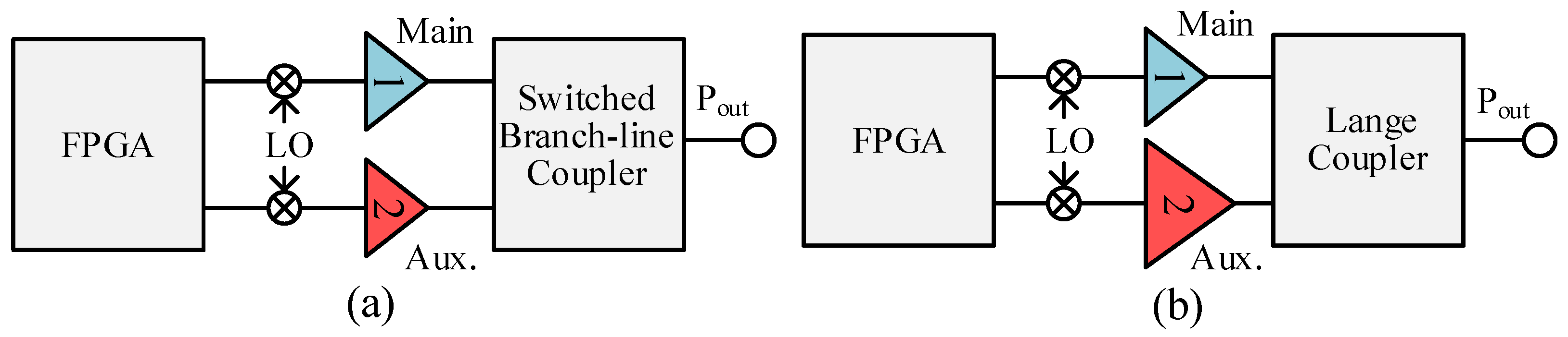
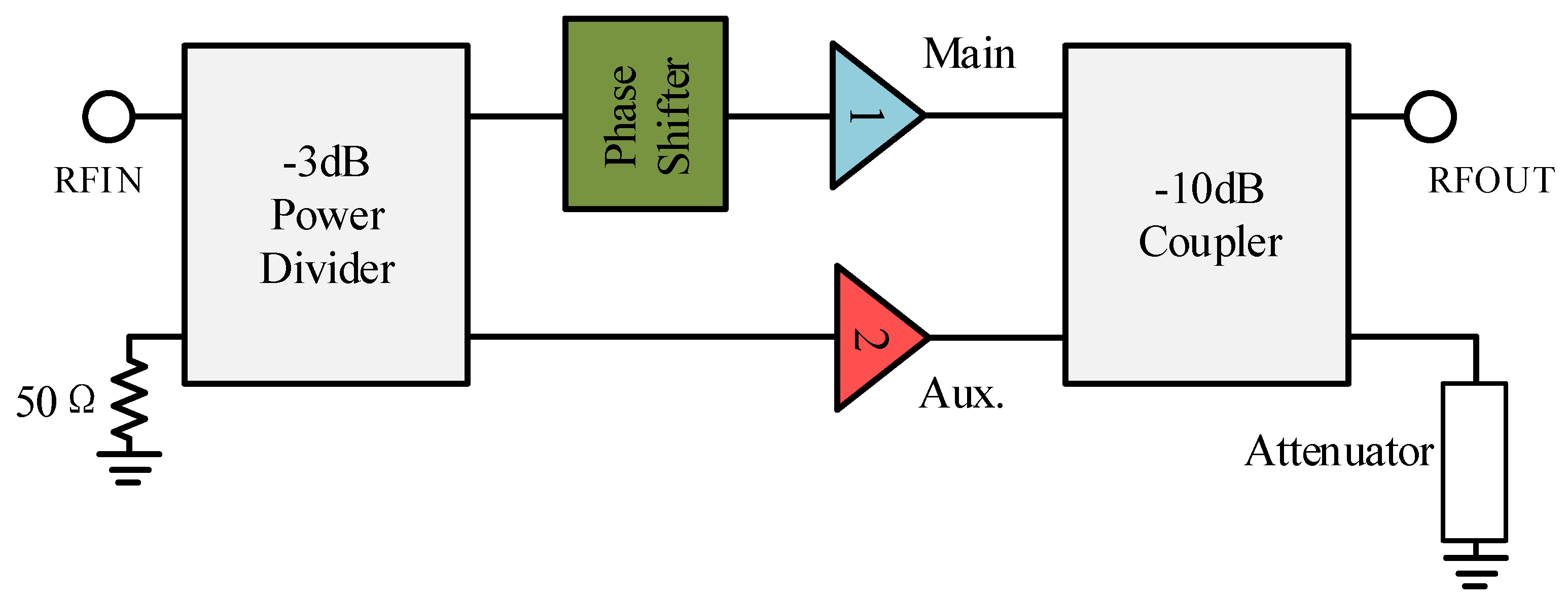
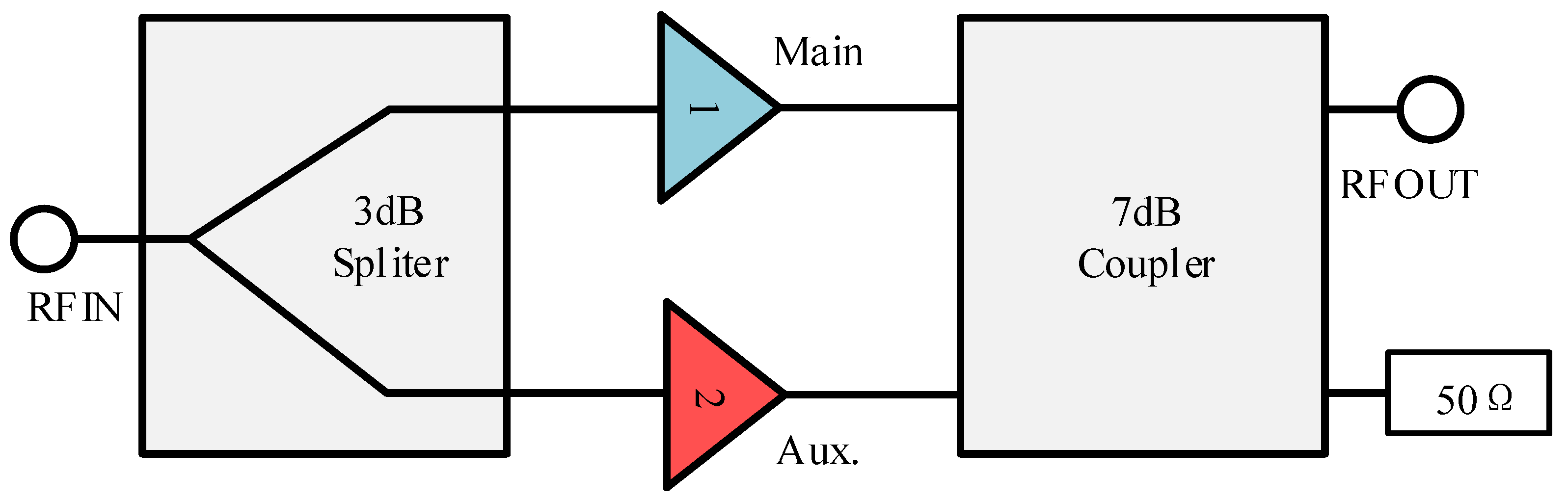
3.1. SPA Based on Coupler
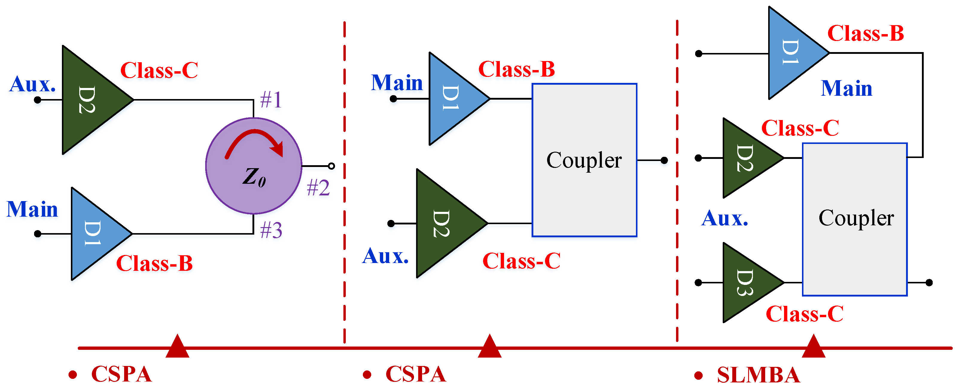
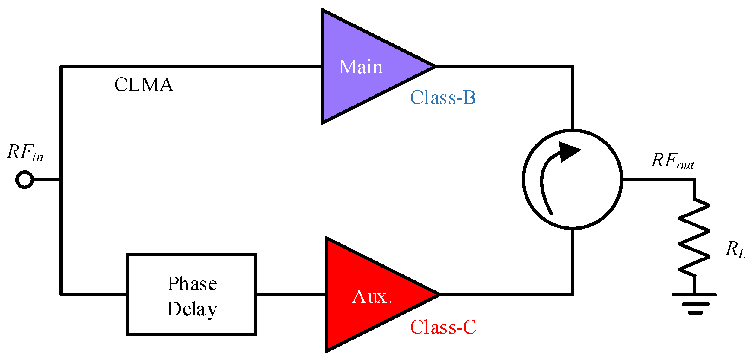
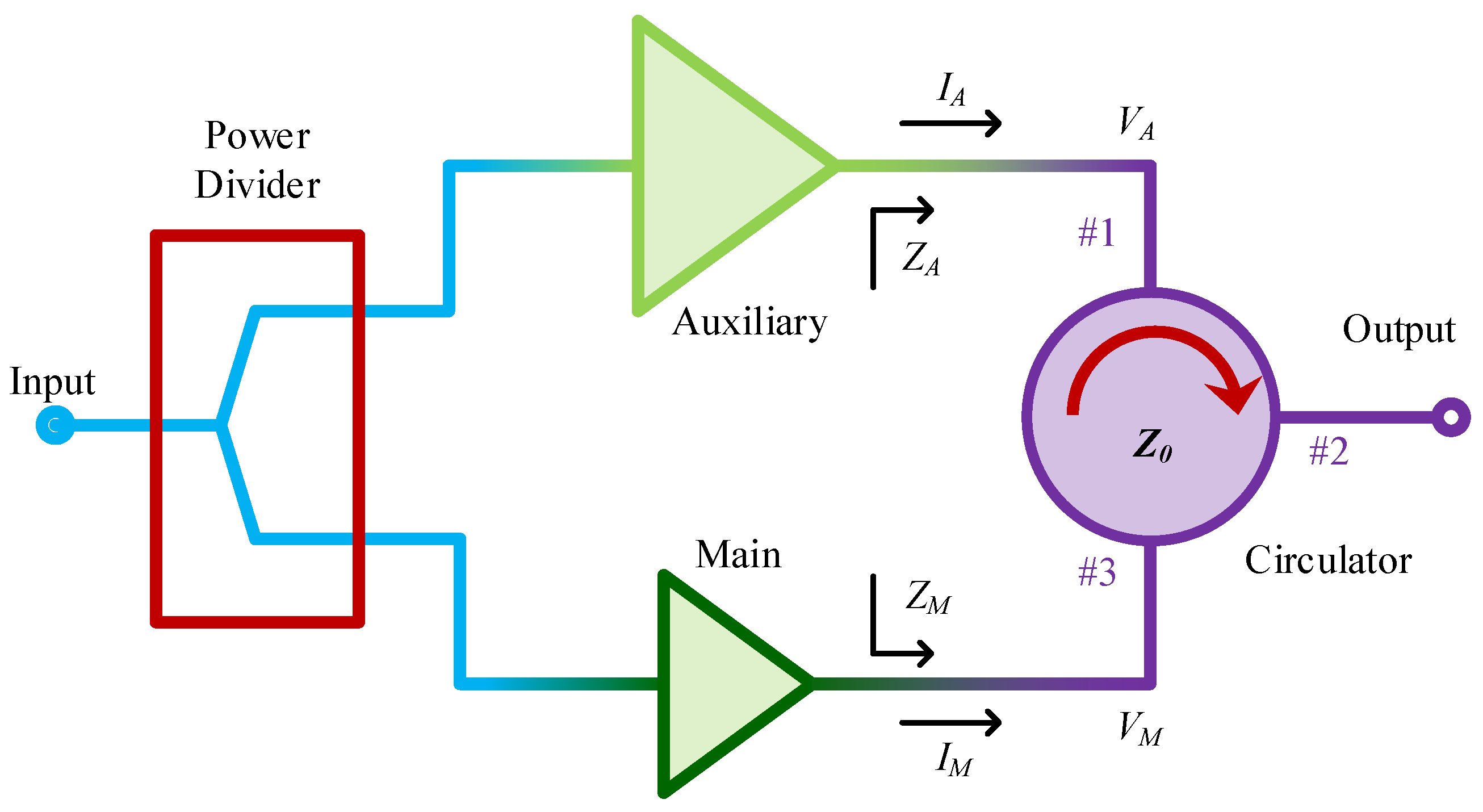
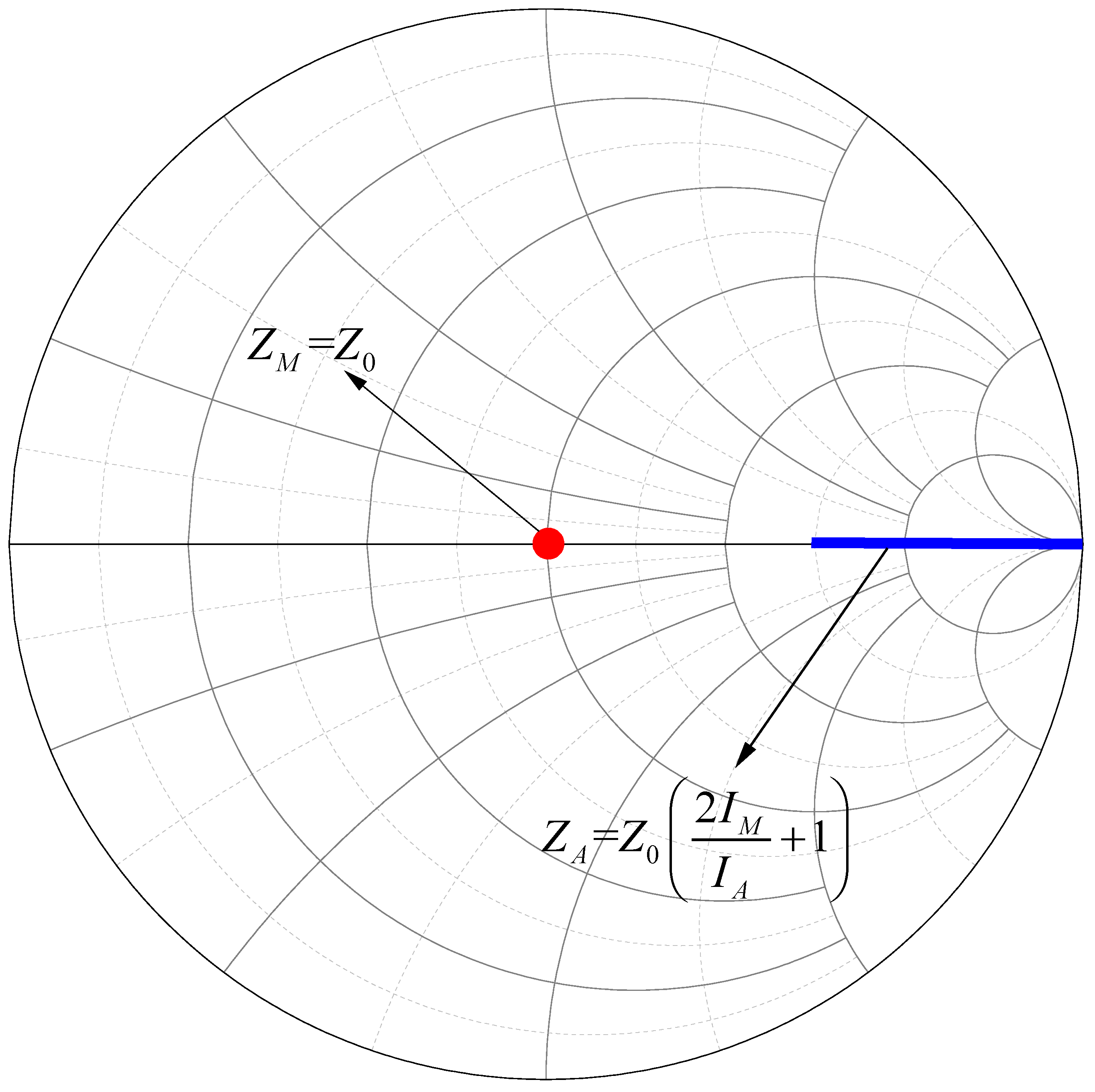
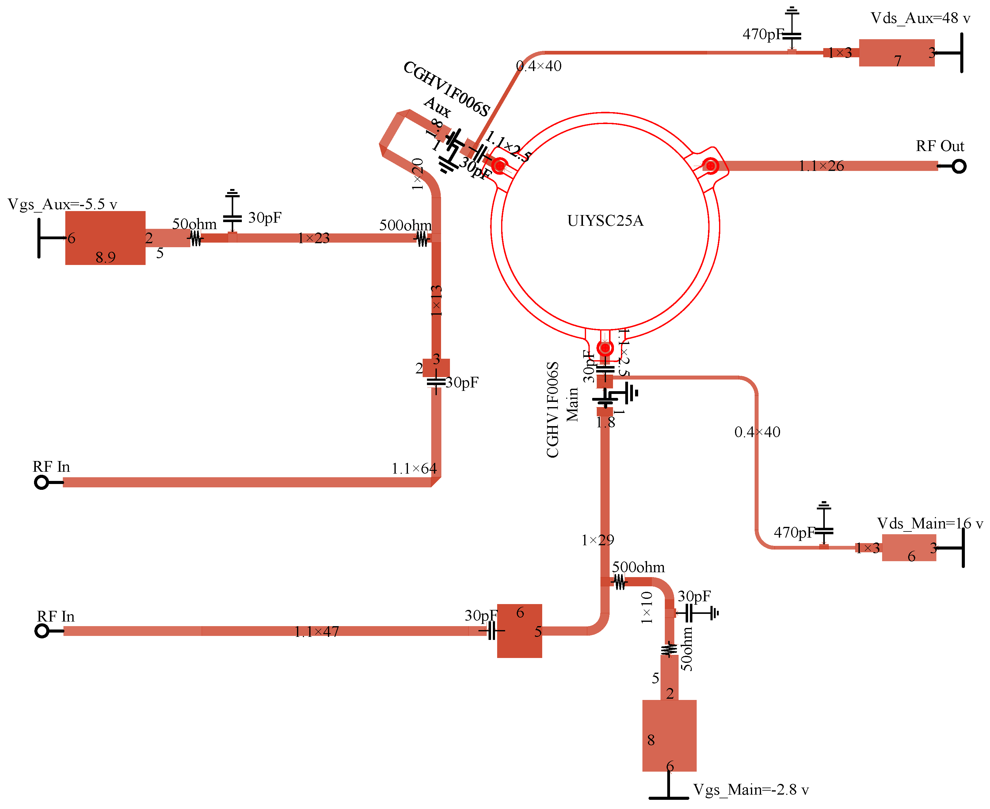
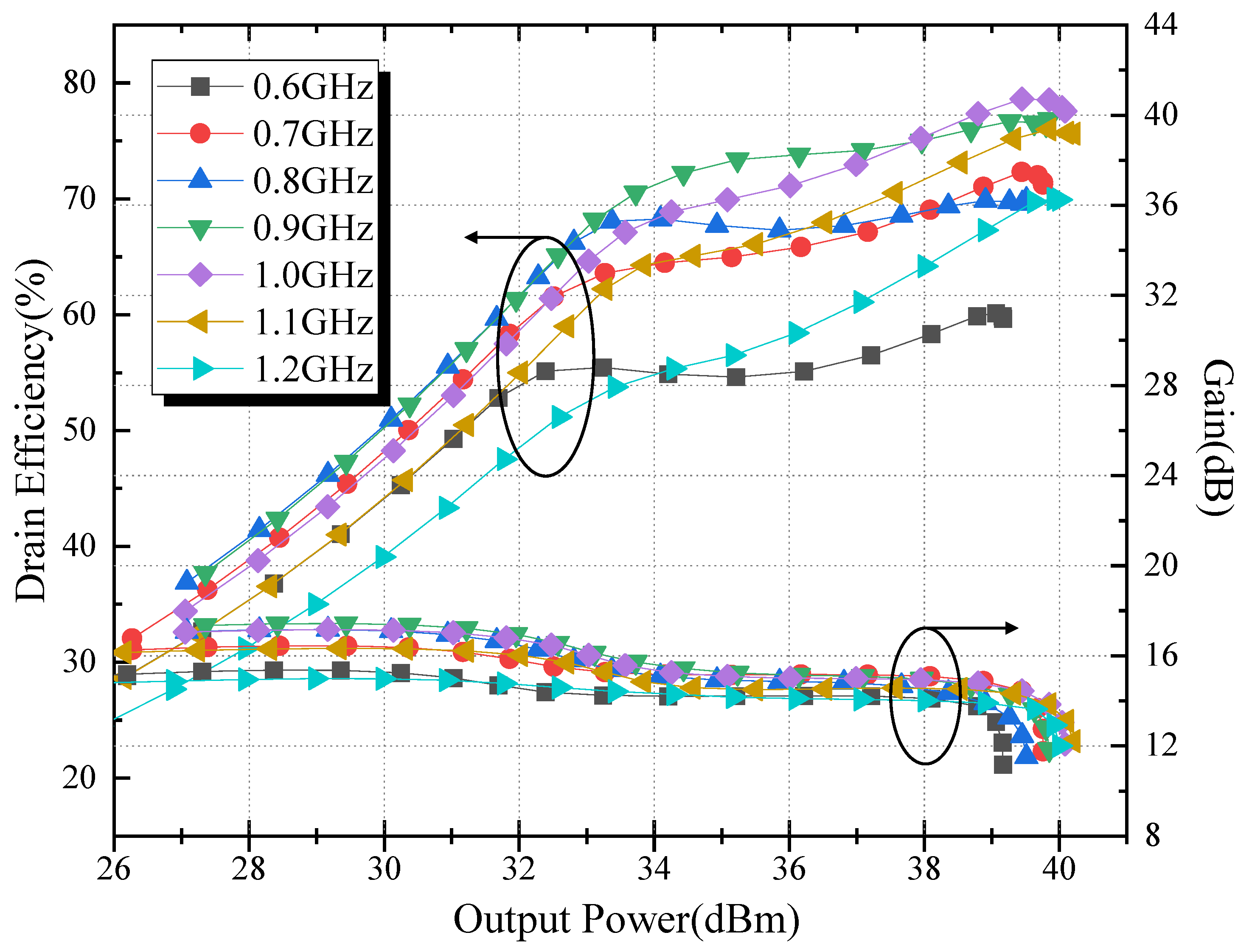
3.2. SPA Based on Circulator
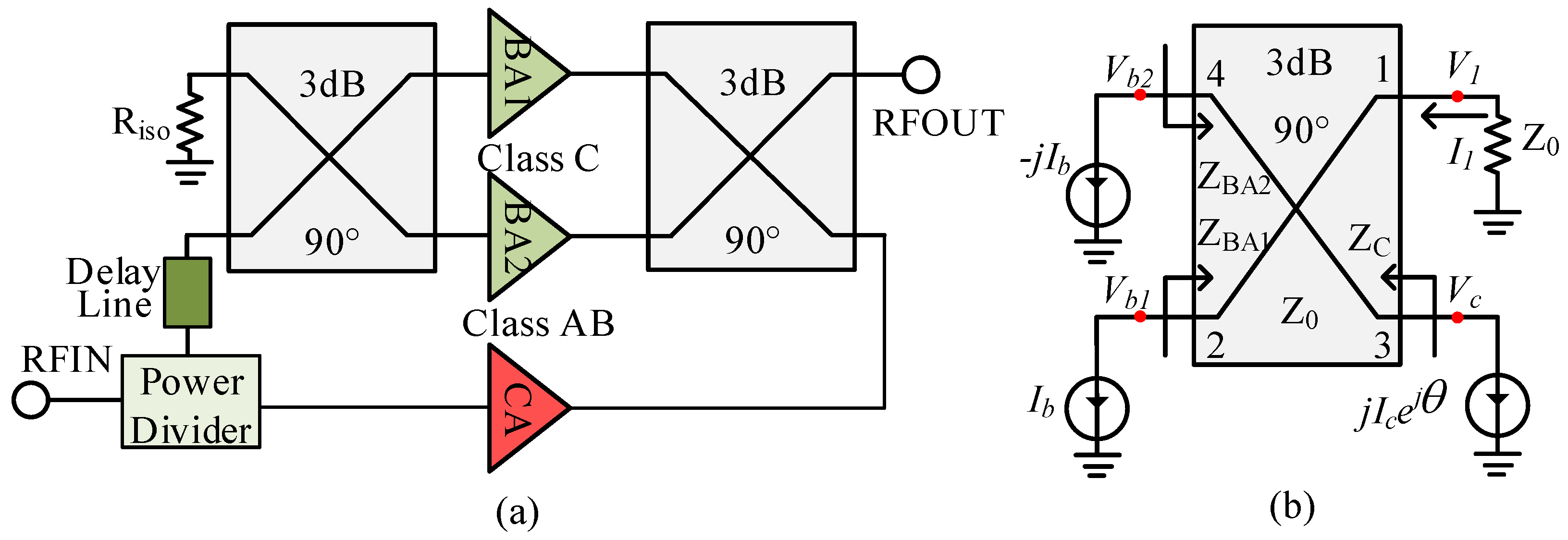
4. Sequential Load Modulated Balanced Amplifier
5. Conclusions
Author Contributions
Funding
Data Availability Statement
Conflicts of Interest
References
- Meng, X.; Kalantari, M.; Chi, B.; Chen, W.; Chen, Z.; Lin, X.; Yue, C.P. A 28-GHz 16-Gb/s high efficiency 16-QAM transmitter in 65-nm CMOS. IEEE Trans. Circuits Syst. I Reg. Pap. 2020, 6, 1835–1845. [Google Scholar] [CrossRef]
- Doherty, W.H. A new high efficiency power amplifier for modulated waves. Proc. IRE 1936, 9, 1163–1182. [Google Scholar] [CrossRef]
- Zhou, X.; Zheng, S.Y.; Chan, W.S.; Chen, S.; Ho, D. Broadband effificiency-enhanced mutually coupled harmonic postmatching Doherty power amplifier. IEEE Trans. Circuits Syst. I Reg. Papers 2017, 7, 1758–1771. [Google Scholar] [CrossRef]
- Camarchia, V.; Pirola, M.; Quaglia, R.; Jee, S.; Cho, Y.; Kim, B. The Doherty power amplifier: Review of recent solutions and trends. IEEE Trans. Microw. Theory Tech. 2015, 2, 559–571. [Google Scholar] [CrossRef]
- Li, M.; Pang, J.; Li, Y.; Zhu, A. Bandwidth enhancement of Doherty power amplifier using modified load modulation network. IEEE Trans. Circuits Syst. I Reg. Papers 2020, 1, 1824–1834. [Google Scholar] [CrossRef]
- Hu, C.; Yang, R.; Shi, W.; Li, L.; Gao, R.; Dai, Z.; Pang, J.; Li, M. Analysis and Design of Broadband Outphasing Power Amplifier Based on Complex Combining Impedance. IEEE Trans. Circuits Syst. I Reg. Papers 2023, 4, 1542–1554. [Google Scholar] [CrossRef]
- Holzer, K.D.; Yuan, W.; Walling, J.S. Wideband techniques for Outphasing power amplifiers. IEEE Trans. Circuits Syst. I Reg. Papers 2017, 65, 2715–2725. [Google Scholar] [CrossRef]
- Wang, W.; Chen, S.; Cai, J.; Zhou, X.Y.; Chan, W.S.; Wang, G.; Xue, Q. A dual-band Outphasing power amplifier based on noncommensurate transmission line concept. IEEE Trans. Microw. Theory Tech. 2020, 7, 3079–3089. [Google Scholar] [CrossRef]
- Shepphard, D.J.; Powell, J.; Cripps, S.C. An efficient broadband reconfigurable power amplifier using active load modulation. IEEE Microw. Wireless Compon. Lett. 2014, 6, 443–445. [Google Scholar] [CrossRef]
- Pednekar, P.H.; Berry, E.; Barton, T.W. RF-input load modulated balanced amplifier with octave bandwidth. IEEE Trans. Microw. Theory Tech. 2017, 65, 5181–5191. [Google Scholar] [CrossRef]
- Pang, J.; He, S.; Huang, C.; Dai, Z.; Peng, J.; You, F. A Post-Matching Doherty Power Amplifier Employing Low-Order Impedance Inverters for Broadband Applications. IEEE Trans. Microw. Theory Tech. 2015, 11, 4061–4071. [Google Scholar] [CrossRef]
- Mannem, N.S.; Huang, T.-Y.; Wang, H. Broadband Active Load-Modulation Power Amplification Using Coupled-Line Baluns: A Multifrequency Role-Exchange Coupler Doherty Amplifier Architecture. IEEE J. Solid-State Circuits 2021, 10, 3109–3122. [Google Scholar] [CrossRef]
- Shi, W.; He, S.; Zhu, X.; Song, B.; Zhu, Z.; Naah, G.; Zhang, M. Broadband Continuous-Mode Doherty Power Amplifiers With Noninfinity Peaking Impedance. IEEE Trans. Microw. Theory Tech. 2018, 2, 1034–1046. [Google Scholar] [CrossRef]
- Lim, J.; Park, C.; Koo, J.; Cha, H.; Jeong, Y.; Han, S.M.; Ahn, D. A balanced power amplifier utilizing the reflected input power. In Proceedings of the 2009 IEEE International Symposium on Radio-Frequency Integration Technology (RFIT), Singapore, 9–11 December 2009; pp. 88–91. [Google Scholar]
- Kurokawa, K. Design Theory of Balanced Transistor Amplifiers. Bell System Tech. J. 1965, 10, 1675–1698. [Google Scholar] [CrossRef]
- Cripps, S.C. RF Power Amplifiers for Wireless Communications, 2nd ed.; Artech House: London, UK, 2006. [Google Scholar]
- Lehmann, T.; Knoechel, R. Wideband Sequential Amplifier with Switched Directional Couplers. In Proceedings of the German Microwave Conference, Hamburg, Germany, 10–12 March 2008; pp. 1–4. [Google Scholar]
- Lehmann, T.; Knoechel, R. Design and performance of sequential power amplifiers. In Proceedings of the 2008 IEEE MTT-S International Microwave Symposium Digest, Atlanta, GA, USA, 15–20 June 2008. [Google Scholar]
- Lehmann, T.; Knoechel, R. Sequential Power Amplifiers with Adaptable Combiners. In Proceedings of the 2009 IEEE MTT-S International Microwave Symposium Digest, Boston, MA, USA, 7–12 June 2009; pp. 425–428. [Google Scholar]
- Merrick, B.; King, J.; Brazil, T. A wideband sequential power amplifier. In Proceedings of the 2014 IEEE MTT-S International Microwave Symposium Digest, Tampa, FL, USA, 1–6 June 2014; pp. 1–3. [Google Scholar]
- Shao, J.; Ma, R.; Teo, K.H.; Shinjo, S.; Yamanaka, K. A fully analog two-way sequential GaN power amplifier with 40% fractional bandwidth. In Proceedings of the IEEE International Wireless Symposium (IWS), Shenzhen, China, 30 March–1 April 2015. [Google Scholar]
- Ren, H.; Shao, J.; Zhou, M.; Arigong, B.; Ding, J.; Kim, H.S.; Zhang, H. Design of a dual-band sequential power amplifier. In Proceedings of the IEEE Topical Conference on Power Amplifiers for Wireless and Radio Applications (PAWR), Austin, TX, USA, 24–27 January 2016; pp. 33–35. [Google Scholar]
- Ozan, S.; Pitt, A.; Nair, M.; Beach, M.A.; Cappello, T. A 47% Fractional Bandwidth Sequential Power Amplifier with High Back-off Efficiency. In Proceedings of the IEEE Middle East and North Africa Communications Conference (MENACOMM), Amman, Jordan, 6–8 December 2022; pp. 37–42. [Google Scholar]
- Zhou, H.; Perez-Cisneros, J.-R.; Fager, C. Circulator load modulated amplifier: A non-reciprocal wideband and efficient PA architecture. In Proceedings of the 2021 IEEE MTT-S International Microwave Symposium (IMS), Atlanta, GA, USA, 7–25 June 2021; pp. 603–605. [Google Scholar]
- Saad, P.; Zhou, H.; Perez-Cisneros, J.-R.; Hou, R.; Fager, C.; Berglund, B. Doherty load modulation based on non-reciprocity. In Proceedings of the 2021 51st European Microwave Conference (EuMC), London, UK, 4–6 April 2022; pp. 938–941. [Google Scholar]
- Zhou, H.; Perez-Cisneros, J.-R.; Fager, C. Wideband sequential circulator load modulated amplifier with back-off efficiency enhancement. In Proceedings of the 2022 52nd European Microwave Conference (EuMC), Milan, Italy, 27–29 September 2022; pp. 214–217. [Google Scholar]
- Yang, R.; Hu, C.; Shi, W.; Pang, J.; Dai, Z.; Li, M. Design of a circulator-based sequential Doherty power amplifier with octave bandwidth and extended dynamic range. In Proceedings of the 2022 2nd International Conference on Frontiers of Electronics, Information and Computation Technologies (ICFEICT), Wuhan, China, 19–21 August 2022; pp. 11–15. [Google Scholar]
- Quaglia, R.; Cripps, S. A load modulated balanced amplifier for telecom applications. IEEE Trans. Microw. Theory Tech. 2018, 3, 1328–1338. [Google Scholar] [CrossRef]
- Pang, J.; Li, Y.; Li, M.; Zhang, Y.; Zhou, X.Y.; Dai, Z.; Zhu, A. Analysis and design of highly efficient wideband RF-input sequential load modulated balanced power amplifier. IEEE Trans. Microw. Theory Tech. 2020, 5, 1741–1753. [Google Scholar] [CrossRef]
- Cao, Y.; Chen, K. Pseudo-Doherty load-modulated balanced amplifier with wide bandwidth and extended power back-off range. IEEE Trans. Microw. Theory Tech. 2020, 7, 3172–3183. [Google Scholar] [CrossRef]
- Cao, Y.; Lyu, H.; Chen, K. Asymmetrical load modulated balanced amplifier with continuum of modulation ratio and dual-octave bandwidth. IEEE Trans. Microw. Theory Tech. 2021, 1, 682–696. [Google Scholar] [CrossRef]
- Cao, Y.; Lyu, H.; Chen, K. Continuous-mode hybrid asymmetrical load-modulated balanced amplifier with three-way modulation and multi-band reconfigurability. IEEE Trans. Circuits Syst. I Reg. Papers 2022, 3, 1077–1090. [Google Scholar] [CrossRef]
- Yang, R.; Shi, W.; Hu, C.; Lin, S.; Dai, Z.; Pang, J.; Li, M. Asymmetrical Sequential Load Modulated Balanced Amplifier with Composited Impedance Inverter and Reciprocal Mode for Broadband Applications. IEEE Trans. Circuits Syst. II Exp. Briefs, 2023; early access. [Google Scholar] [CrossRef]


| Ref., Year | Freq. (GHz) | BW. (GHz/%) | Pmax (dBm) | DE@Sat (%) | OBO (dB) | DE@OBO (%) |
|---|---|---|---|---|---|---|
| 2014 [20] | 1.45–2.4 | 0.95/49 | 43–45 | 35–44 | 3 | 54–65 |
| 2015 [21] | 2.1–2.9 | 0.8/32 | 39.5 | 26–34 | 5 | 45–61 |
| 2015 [22] | 1.1/1.5 | NA | 39.3/40.5 | 62/65 | 6 | 48/62 |
| 2022 [23] | 2.9–4.7 | 1.8/47 | 40–42 | 43–56 | 8 | 36–52 |
| Ref., Year | Freq. (GHz) | BW. (GHz/%) | Pmax (dBm) | DE@Sat (%) | OBO (dB) | DE@OBO (%) |
|---|---|---|---|---|---|---|
| 2021 [24] | 2.09 | NA | 43.1 | 73.2 | 6 | 73 |
| 2022 [26] | 2.0–3.0 | 2.0/40 | 42–43.5 | 55–68 | 8 | 46–53 |
| 2022 [27] | 0.6–1.2 | 0.6/67 | 39.1–40.2 | 59.7–78.6 | 8 | 47.7–62.5 |
| Ref., Year | Freq. (GHz) | BW. (GHz/%) | Pmax (dBm) | DE@Sat (%) | OBO (dB) | DE@OBO (%) |
|---|---|---|---|---|---|---|
| 2020 [29] | 3.05–3.55 | 0.5/15 | 42.3–43.7 | 60.8–74.8 | 10 | 43.2–51.4 |
| 2020 [30] | 1.5–2.7 | 1.2/57 | 41–43 | 58–72 | 10 | 47–58 |
| 2022 [32] | 1.7–3.0 | 1.3/55 | 42–43 | 63–81 | 10 | 50–66 |
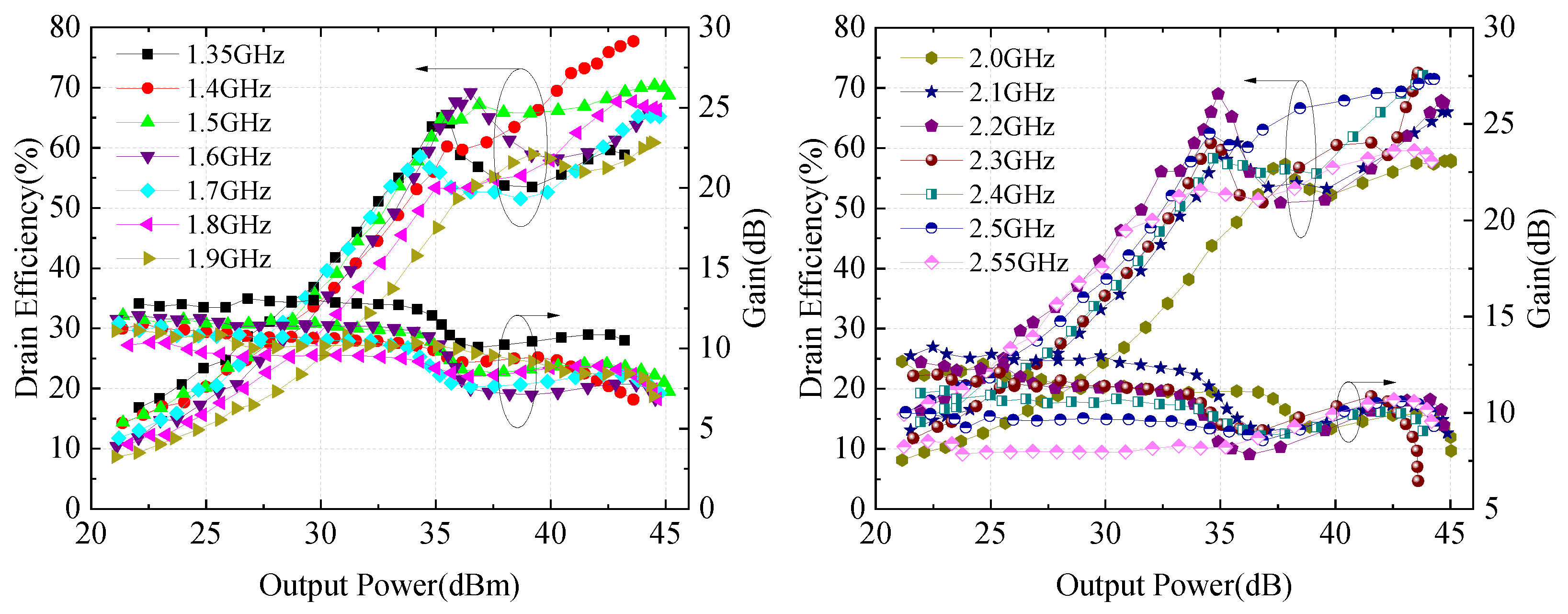
| 2023 [33] | 1.35–2.55 | 1.2/62 | 43.2–45.1 | 57.8–77.7 | 10 | 47.7–68.9 |
Disclaimer/Publisher’s Note: The statements, opinions and data contained in all publications are solely those of the individual author(s) and contributor(s) and not of MDPI and/or the editor(s). MDPI and/or the editor(s) disclaim responsibility for any injury to people or property resulting from any ideas, methods, instructions or products referred to in the content. |
© 2023 by the authors. Licensee MDPI, Basel, Switzerland. This article is an open access article distributed under the terms and conditions of the Creative Commons Attribution (CC BY) license (https://creativecommons.org/licenses/by/4.0/).
Share and Cite
Yang, K.; Yang, R.; Zhang, P.; Shi, W.; Hu, C.; Shi, W. Development Review of Highly Efficient Sequential Power Amplifier with Extended Back-Off Range for Broadband Application. Energies 2024, 17, 161. https://doi.org/10.3390/en17010161
Yang K, Yang R, Zhang P, Shi W, Hu C, Shi W. Development Review of Highly Efficient Sequential Power Amplifier with Extended Back-Off Range for Broadband Application. Energies. 2024; 17(1):161. https://doi.org/10.3390/en17010161
Chicago/Turabian StyleYang, Keyuan, Rongxing Yang, Pan Zhang, Wei Shi, Chunyu Hu, and Weimin Shi. 2024. "Development Review of Highly Efficient Sequential Power Amplifier with Extended Back-Off Range for Broadband Application" Energies 17, no. 1: 161. https://doi.org/10.3390/en17010161
APA StyleYang, K., Yang, R., Zhang, P., Shi, W., Hu, C., & Shi, W. (2024). Development Review of Highly Efficient Sequential Power Amplifier with Extended Back-Off Range for Broadband Application. Energies, 17(1), 161. https://doi.org/10.3390/en17010161