Article

An Energy-Feed Type Split-Capacitor Three-Phase Four-Wire Power Electronic Load Compatible with Various Load Demands

1
State Key Laboratory of Disaster Prevention & Reduction for Power Grid, Changsha 410129, China
2
Disaster Prevention and Reduction Center of Hunan Electric Power Co., Ltd. of State Grid, Changsha 410129, China
3
School of Automation, Wuhan University of Technology, Wuhan 430070, China
4
School of Automation, Wuhan University of Science and Technology, Wuhan 430081, China
*
Author to whom correspondence should be addressed.
Energies 2024, 17(1), 119; https://doi.org/10.3390/en17010119
Submission received: 16 November 2023 / Revised: 17 December 2023 / Accepted: 20 December 2023 / Published: 25 December 2023
(This article belongs to the Special Issue Advances in Power Electronics Technologies)

Abstract

:
Energy-feed power electronic loads can precisely control the phase and magnitude of the power supply output current, achieving the emulation of loads. Moreover, they can feed energy back to the grid for energy regeneration, demonstrating significant research value. This article proposes an energy-fed power electronic load topology and control method that can realize the static and dynamic simulation of linear and non-linear loads and take into account the simulation needs of single-phase, three-phase three-wire, and three-phase four-wire loads. The main circuit uses a two-stage back-to-back AC/DC/AC structure: the front side is a three-phase four-wire split capacitor PWM rectifier bridge, which is used to simulate loads under various operating conditions; the back side is a three-phase three-wire PWM inverter bridge, which realizes the energy feeding back to the grid and reduces the waste of energy; and the intermediate side uses a split capacitor to equalize the voltage and achieve voltage stabilization. The topology is analyzed under the simulation demands of three-phase balanced, three-phase unbalanced, single-phase and non-linear loads. Finally, a MATLAB(R2022a)/Simulink simulation platform is built for a power electronic load with a rated capacity of 200 kVA. The simulation results verify the effectiveness, feasibility, and advancement of the power electronic load proposed in this article.

1. Introduction

With the advancement of power electronics technology and the continuous improvement of various switch device performances, the quality of power supply has become a direct constraint on the development of production and life [1]. Therefore, numerous domestic and international standards have been established for assessing the performance indicators of various power supply devices, especially regarding power system harmonic issues. The Institute of Electrical and Electronics Engineers (IEEE) in the United States, in collaboration with the International Electrotechnical Commission (IEC), has formulated a series of international harmonic standards (IEEE 519-1992, IEC 1000-2-2, IEC 1000-3-6, IEC 1000-3-3, IEC 1000-3-5). Other standards include UPSIEC62040 for applications in finance and communication, as well as the domestic standard GB/T 7260.3-2003 for Uninterruptible Power Supply (UPS) devices. Additionally, military standards like GJB572-88 address aircraft ground power supply characteristics and general requirements.
Before leaving the factory, power supplies undergo various load experiments, including aging tests, electrical characteristic tests, and dynamic load tests, to assess their technical specifications and reliability [2]. Traditional testing methods involve combining resistors, inductors, and capacitors in series or parallel configurations based on testing requirements. However, this traditional approach has drawbacks, such as the inability to achieve continuous adjustment during load testing, low efficiency, 100% energy consumption during testing leading to aging-related fire risks, the need for large spaces and dedicated cooling equipment, and the absence of remote monitoring capabilities.
The essence of power supply testing is to control the actual output current of the power supply, ensuring that the relationship between the power supply voltage and output current satisfies the corresponding load conditions, thereby detecting the performance of the power supply under various specific load scenarios. In line with this concept, connecting a set of power electronic conversion devices to the tested power supply and precisely controlling the phase and magnitude of the output current effectively simulates a real load for testing purposes. This constitutes the initial concept of an electronic load [3]. If the output current of the power supply is controlled on one side to satisfy the corresponding load relationship with the voltage, and on the other side, the test energy is inverted and fed back to the power grid, this achieves both power supply testing and energy savings, representing the concept of power electronic loads.
The overall structure of a power electronic load consists of two stages. The front stage is the Load Simulation Converter (LSC), connected to the Devices Be Test (DBT) for simulating the load. The rear stage is the Energy Feedback Converter (EFC), connected to the three-phase power grid for energy feedback. By adopting a two-stage structure with separate control, energy consumption during the entire testing process is limited to the power devices, significantly saving energy [4].
Compared to traditional loads, power electronic loads offer advantages in continuous load adjustment, space efficiency, cost savings, reduced maintenance, and energy conservation through feedback to the power grid. Given these advantages, particularly in simulating arbitrary loads, saving energy, and reducing costs, power electronic loads present significant research implications and broad market prospects [5,6].
Traditional electrical loads consist of passive components such as resistors, capacitors, and inductors [7]. However, conventional test loads suffer from drawbacks such as the inability to continuously adjust, limited load characteristics, low simulation accuracy, and high energy consumption. Connecting a set of power electronic converter devices to the tested power source and precisely controlling the phase and magnitude of the power source output current is equivalent to applying a real load from the power source perspective. This achieves the purpose of simulating a load, known as regenerative electronic load [8,9]. Regenerative electronic loads are commonly used in DC power testing, where the tested DC energy is inverted into AC and fed back into the grid for energy regeneration. This device offers advantages such as energy savings, compact size, lighter weight, space-saving installation, and excellent testing performance [10,11].
In 1990, reference [12] proposed an aging testing device for UPS, which had a relatively fixed application scenario. Reference [13] achieved the regulation of active and reactive power of the three-phase test power supply. Subsequently, the application of various DC power sources led experts to conduct extensive research on the power electronic loads used for their testing, ranging from using DC/AC converters to connect to the power grid to control the output power of the tested power source to adding Boost, Buck, and Cuk converters to increase the function of feedback energy to the power grid. The prototype of energy-fed power electronic loads has taken shape [14,15,16]. Reference [17] proposes a study on three-phase energy-fed AC electronic loads based on dual PWM converters, taking the research on three-phase energy-fed electronic loads one step closer. Reference [18] proposes an AC power electronic load composed of two-stage AC/DC converters, and its back-to-back structure has gradually gained recognition, laying the foundation for research on power electronic loads in recent years.
However, the existing research on energy-fed AC electronic loads mainly focuses on the design of single-phase or three-phase balanced working conditions, making it difficult to balance load testing under various working conditions such as three-phase three-wire, three-phase four-wire, and single-phase. Reference [19] has conducted preliminary research on the control scheme of single-phase energy-fed AC electronic loads, but it is difficult to meet other working conditions. Reference [20] proposes an energy feedback electronic load that uses harmonic compensation to reduce harmonic interference in the power grid, which can improve energy feedback efficiency. At present, further research is needed on energy-fed AC electronic loads to ensure that their input characteristics are completely consistent with various typical load impedances corresponding to actual on-site conditions, and to flexibly simulate the steady-state operation of single-phase, three-phase balanced, and three-phase unbalanced loads, as well as the dynamic changes in load sudden changes.
This article proposes an energy-fed three-phase four-wire power electronic load using a front-end split capacitor rectifier based on SPWM control to meet the requirements of compatible simulation of multiple loads and analyzes the system operation status under various working conditions. Finally, the feasibility of this topology structure is verified by building a simulation model.

2. Materials and Methods

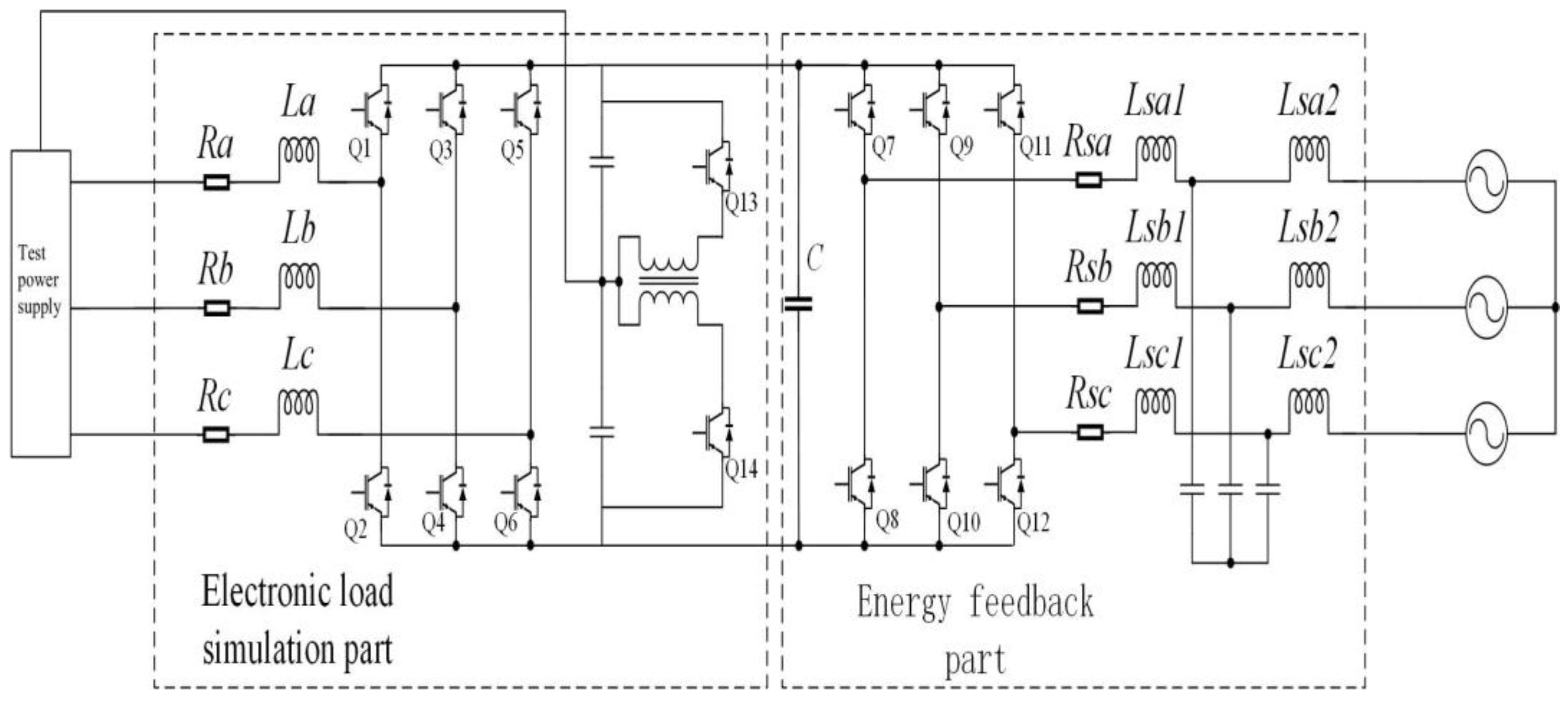
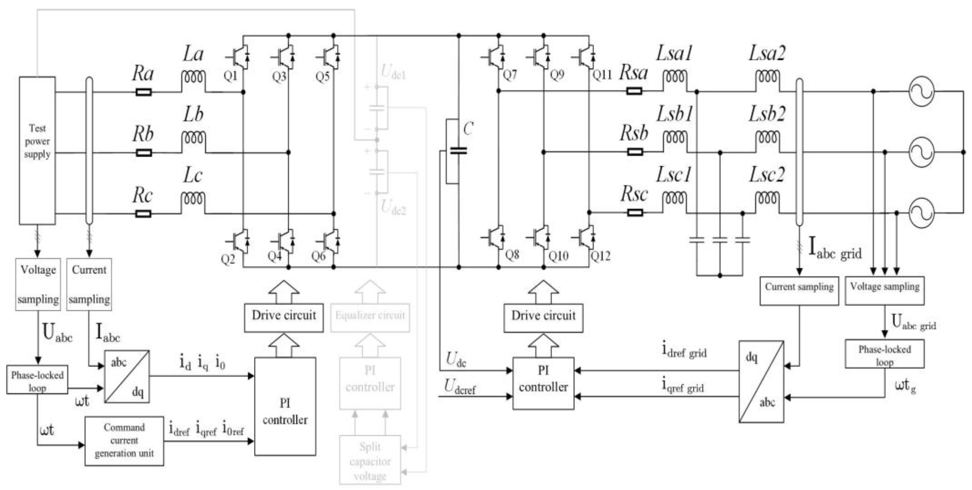
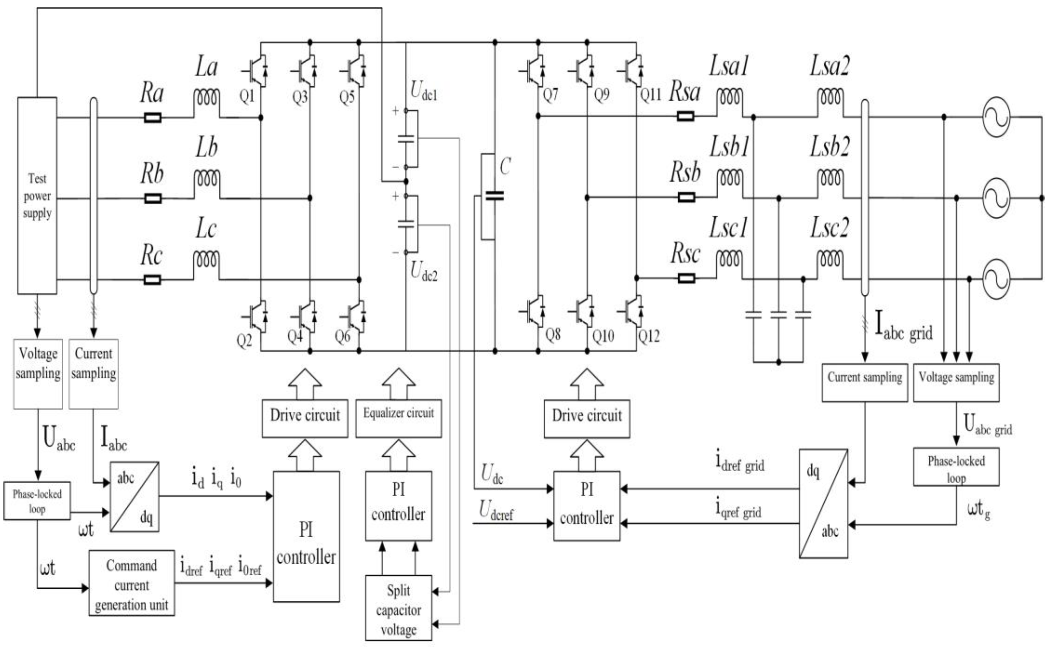
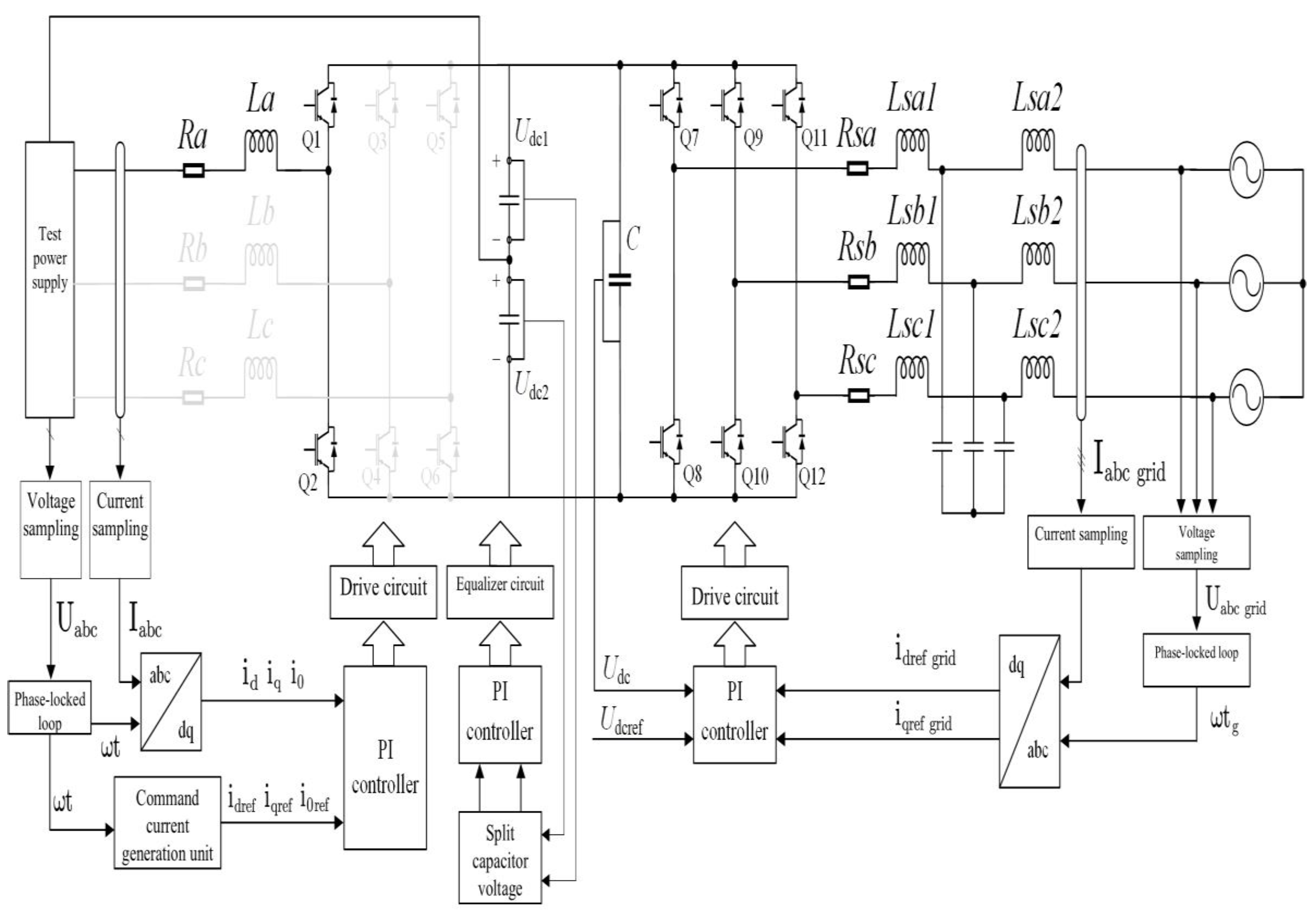
2.1. Topological Structure of Three-Phase Four-Wire Split Capacitor Power Electronic Load

This article addresses the two primary issues with traditional three-phase power electronic loads: the inability to simultaneously simulate single-phase loads and unbalanced three-phase loads, as well as the poor simulation performance for nonlinear loads. The proposed solution is the three-phase four-wire split-capacitor power electronic load, as depicted in Figure 1.
It comprises two main components:
(1)
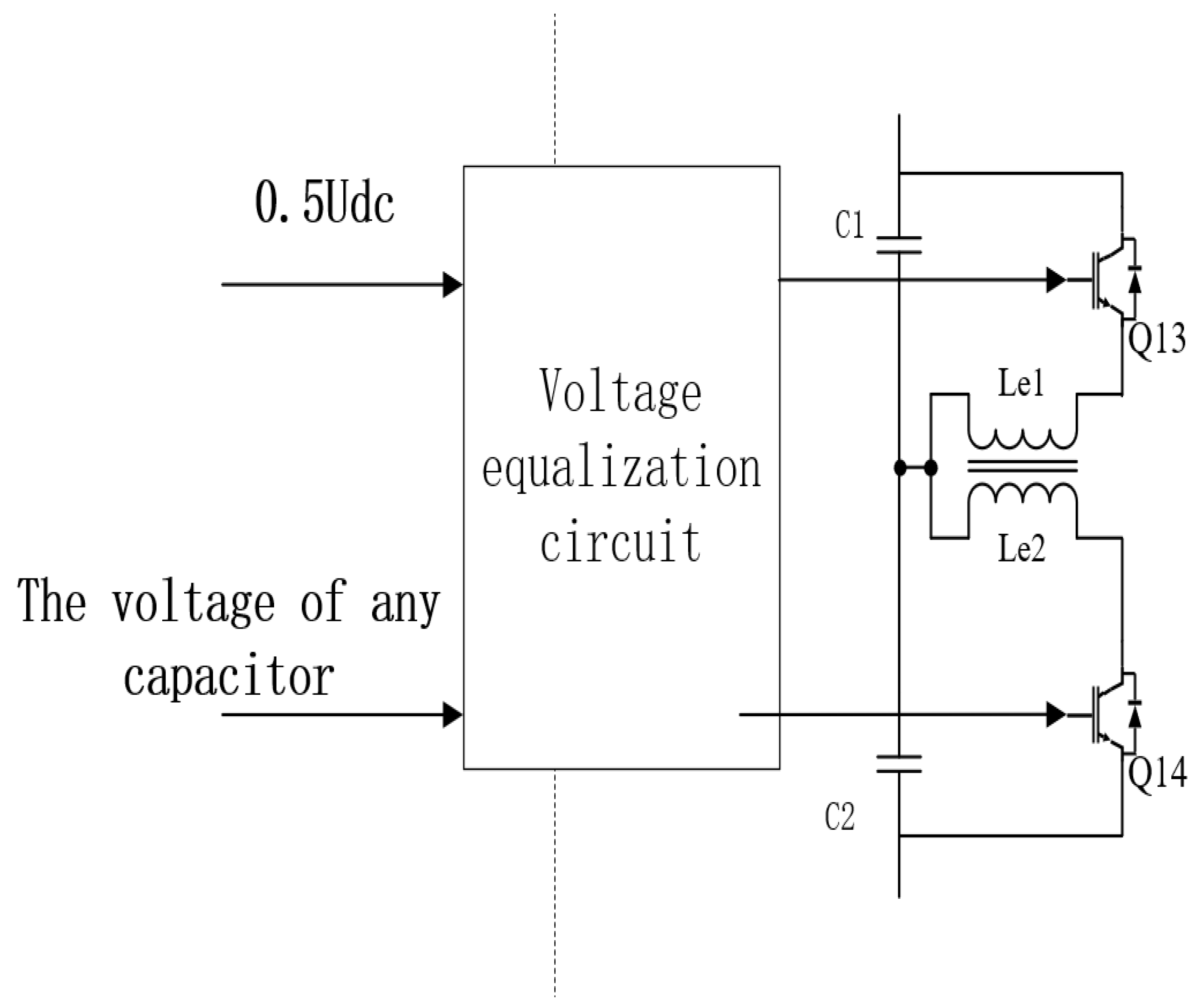
Electronic Load Simulation Part: Essentially a three-phase PWM rectifier, it employs a current direct control method to precisely track the commanded current, ensuring that the power supply output current satisfies the corresponding load relationship with the power supply voltage. This achieves the goal of simulating the load. The testing power supply is a three-phase balanced power supply with an effective value of 220 V. Three-phase inductors (La, Lb, Lc) act as harmonic filters, enabling the three-phase current to meet grid requirements. Q1~Q6 are power switch devices (IGBTs) chosen to handle the high line current and voltage levels of the entire system. Two split capacitors maintain the stability of the DC bus voltage under conditions of unbalanced three-phase loads and nonlinear loads. The capacitor values are set to typical DC bus capacitance values, and a flyback equalization strategy is employed, with two IGBTs and a set of transformers connected in parallel at both ends of the split capacitors to equalize the voltage.
(2)
Energy Feedback Part: Essentially a three-phase PWM inverter, it utilizes a control method with DC voltage as the outer loop and current as the inner loop. The energy stored in the capacitors is converted into AC and fed back into the grid through the inverter, regulating the grid current power factor to achieve grid energy quality regulation and energy feedback goals. Q7~Q12 use IGBTs as power switch devices, and a classical LCL filter is selected for effective filtering.
In order to ensure the inverter’s connection to the grid, it is imperative to synchronize the inverter operation with the grid and ensure that the inverter’s output current and voltage meet the grid requirements. To achieve these objectives, a phase-locked loop module is employed in the control section to acquire the grid’s voltage and frequency, thereby ensuring synchronization between the inverter and the grid. Additionally, a filtering section comprising inductance–capacitance–inductance elements is introduced in the inverter-grid connection segment. This filtering section is designed to enhance the quality of the inverter’s output current and voltage, aligning them with the grid requirements. It is essential to judiciously configure the circuit parameters of the front-end rectifier and the control parameters to ensure that the total harmonic distortion (THD) of the three-phase line current remains below 5%. By following these steps, the inverter can be securely connected to the grid.

2.2. The Analysis of the Operational States of the Three-Phase Four-Wire Split-Capacitor Power Electronic Load

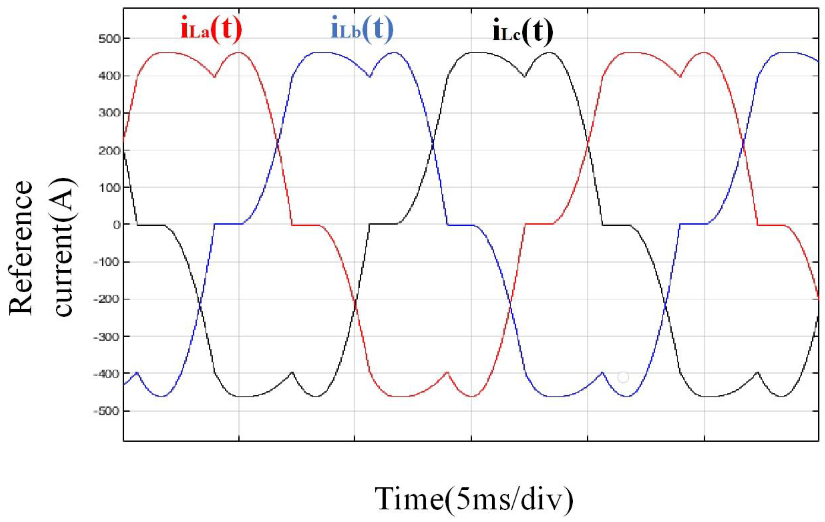
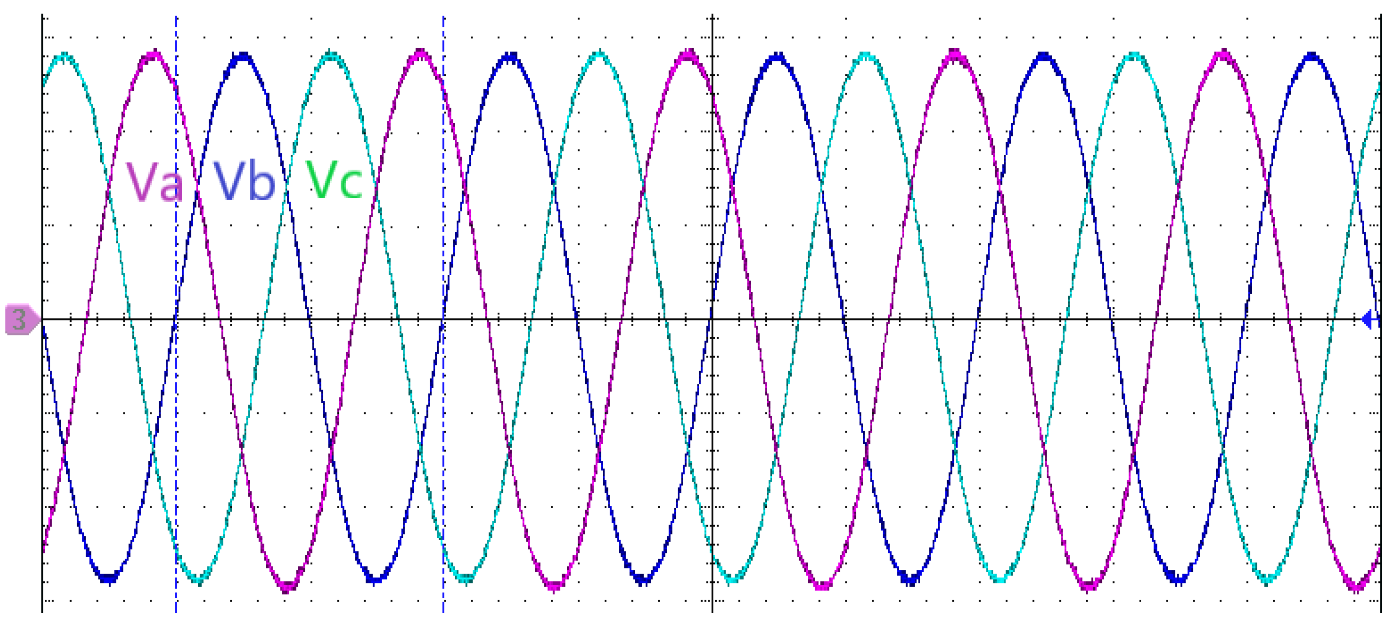
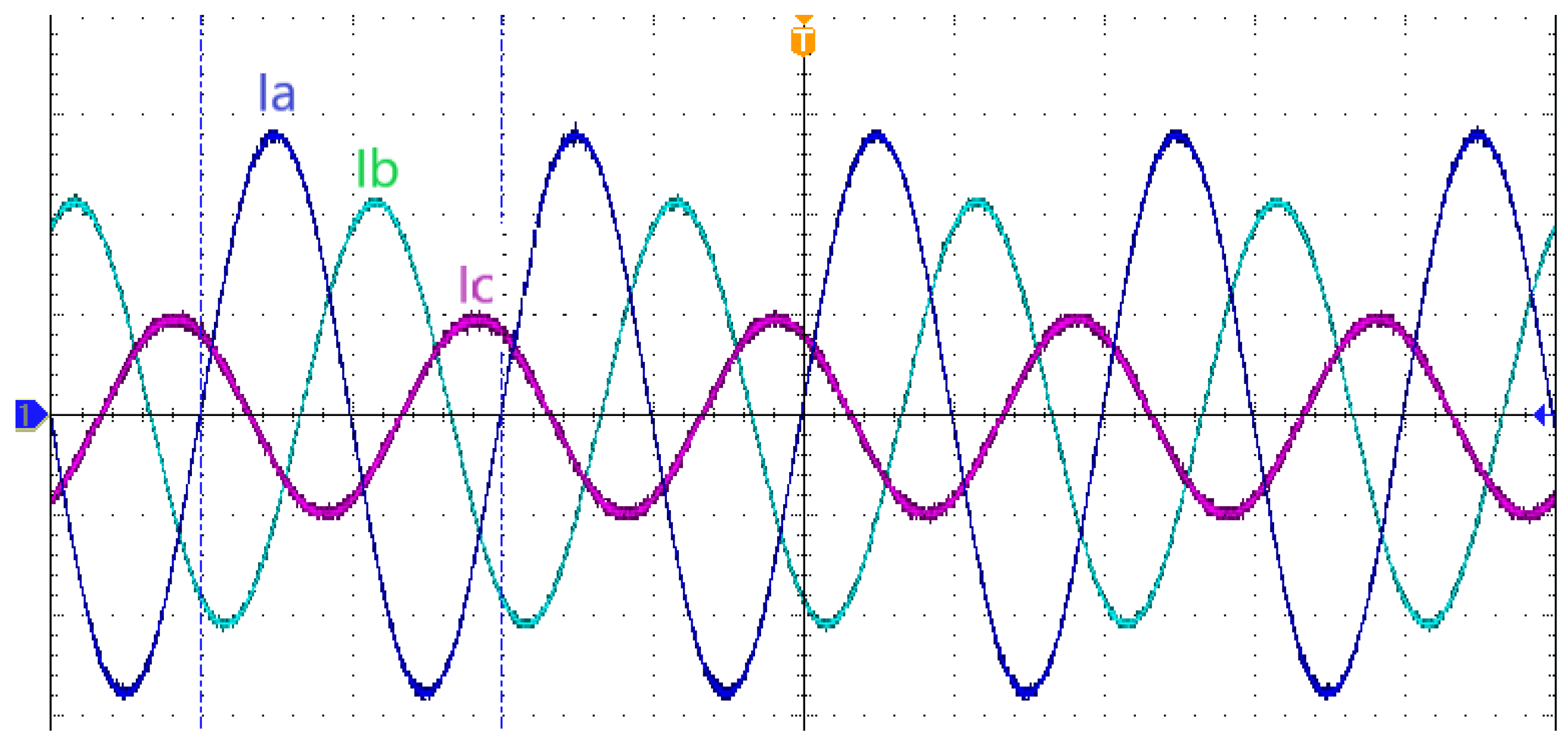
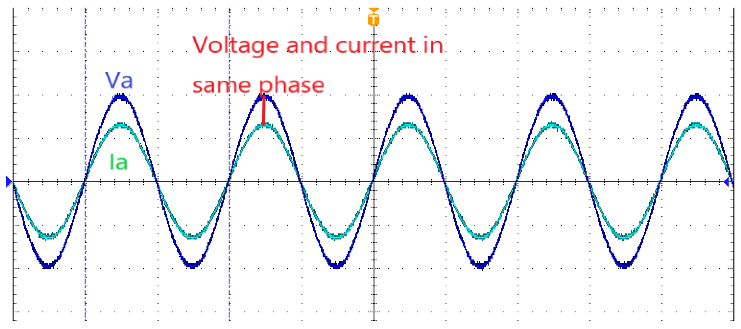
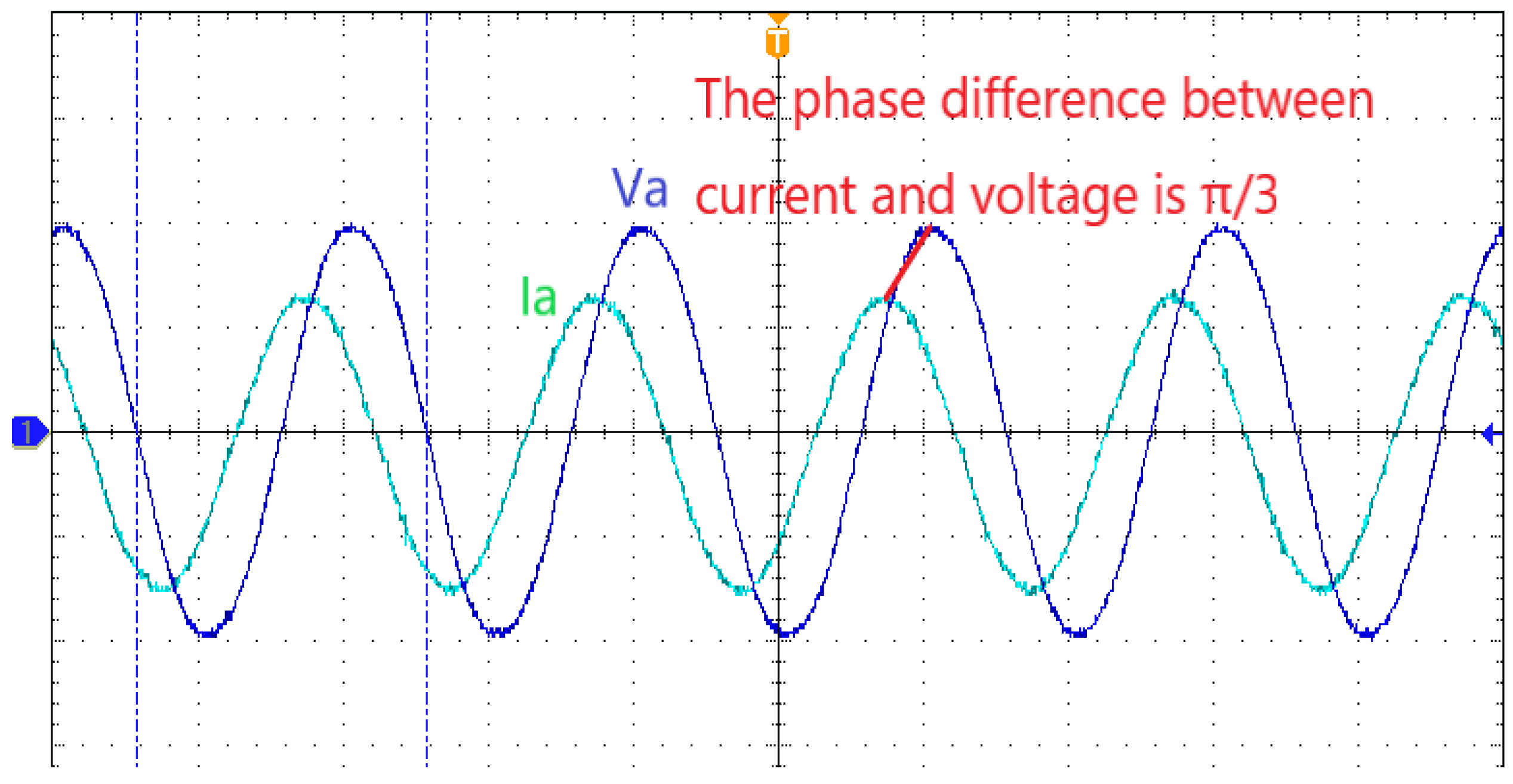
2.2.1. Simulation of Three-Phase Balanced Loads

In the context of simulating a three-phase balanced load, the given topology employs an instruction current generation unit to produce three-phase sinusoidal currents of equal magnitude with a phase difference of 120°. For the power source, the latter part is akin to connecting a set of three-phase balanced loads. Under such circumstances, no zero-sequence or negative-sequence currents are generated in the system. Consequently, there is no requirement for the involvement of split capacitors in the fourth bridge arm, and there is no need to regulate the voltage across the balanced split capacitors. The circuit configuration during the simulation of a three-phase balanced load is illustrated in Figure 2.
In this scenario, the system’s controller primarily comprises three components:
(1)
Phase-Locked Loop (PLL): This module is employed to detect the phase of the power source voltage. The detected phase is utilized in the instruction current generation unit and the coordinate transformation stage. Serving as the foundation of the entire control section, the PLL ensures that the instruction current generation unit produces the requisite three-phase balanced currents to emulate a three-phase balanced load. Moreover, it ensures that the grid side achieves a unity power factor for grid connection.
(2)
Command current generation circuit: Utilizing the previously acquired power source voltage phase, this circuit generates specified currents necessary for simulating a three-phase balanced load.
(3)
Drive circuit: Through coordinate transformation techniques, the currents in the abc coordinate system are converted to the dq0 coordinate system. The PI controller and Space Vector Pulse Width Modulation (SPWM) control generate switch signals for the circuit, which are then delivered to six IGBTs. These signals control the IGBTs’ conduction and switching, enabling the actual current in the circuit to closely approximate the instruction current.
The system detects the circuit by transmitting the test power source voltage Uabc to the control circuit. The instruction current generation circuit generates the corresponding instruction current Iref based on the type of load. By comparing the actual output current I of the test power source with the instruction current Iref, the controller generates drive signals to control the operation state of the load simulation converter accurately, ensuring that the actual output current of the test power source accurately tracks the corresponding instruction current, thereby achieving the goal of simulating a specific load. The test energy is transferred to the energy feedback converter through the intermediate DC bus capacitor. Simultaneously, the controller adjusts the grid-feeding current to achieve a phase difference of 180° with the grid voltage, thereby achieving unity power factor grid connection and realizing energy-saving objectives [21,22].

2.2.2. Simulation of Three-Phase Unbalanced Loads and Non-Linear Loads

When simulating a three-phase unbalanced load, a modification to the conventional three-phase three-wire topology involves the splitting of the DC-side capacitors to form a neutral point, providing a pathway for zero-sequence currents. Due to the presence of the neutral point, the sum of the three-phase currents (Ica, Icb, Icc) is not zero, indicating the existence of a neutral line current (Icn). Due to the presence of Icn, imbalance occurs in the voltages across the two split capacitors on the DC side, denoted as Udc1 and Udc2. This imbalance adversely affects the load simulation performance, grid integration performance, and overall system longevity. To mitigate this, an additional voltage equalization circuit is introduced for the split capacitors, reducing the voltage difference between them and thereby enhancing simulation performance and energy quality.
In this scenario, after obtaining the phase of the power source voltage through the phase-locked loop, it is necessary to introduce a phase lag or lead between the instruction and the power source voltage phases. This adjustment is essential to simulate capacitive or resistive loads. The operation of other modules is fundamentally similar to simulating a three-phase balanced load. The circuit configuration during the simulation of a three-phase unbalanced load is illustrated in Figure 3.
When simulating a nonlinear load, the circuit’s three-phase input currents exhibit an imbalance. Therefore, the circuit topology remains consistent with the structure described earlier for simulating three-phase unbalanced loads. The only modification required is adjusting the waveforms in the three-phase unbalanced instruction current circuit to represent the given current waveforms for the nonlinear load scenario. This adjustment enables the circuit’s front-end to operate in a state simulating a nonlinear load. The specified current waveforms for simulating nonlinear loads are depicted in Figure 4.
In both of the aforementioned scenarios, the existence of Icn introduces an imbalance in the voltages across the two split capacitors on the DC side, necessitating the addition of a voltage equalization circuit for the split capacitors. Commonly employed circuits for voltage equalization include forward and flyback circuits. In the case of a forward circuit, residual magnetic field energy is inherently present due to hysteresis, requiring a dedicated time for demagnetization. In comparison to the flyback circuit topology, the forward circuit demands more components due to the need for an additional magnetic core reset circuit. Taking these factors into consideration, this study opts for the application of the flyback principle and devises a topology suitable for voltage equalization across split capacitors. The specific approach involves taking the difference between the voltage across any split capacitor and half of the DC voltage. This difference is then processed through a PI controller, and the resultant output is compared with a carrier wave before generating the corresponding drive signals. This methodology effectively reduces the operating frequency of the switching devices. The control strategy for the capacitor voltage equalization topology is illustrated in Figure 5.

2.2.3. Simulation of Single-Phase Loads

When simulating single-phase loads, any one phase (ABC) is chosen as one side of the path, with the fourth bridge arm serving as the path for the other side, while the remaining two phases are kept normally closed. At this point, the front-end circuit structure forms a single-phase half-bridge rectifier. By controlling the two switching devices, simulation of a single-phase load can be achieved. The circuit state during the simulation of a single-phase load is illustrated in Figure 6.

3. Results

To validate the correctness and feasibility of the aforementioned circuit structure, this study constructed a simulation model of a three-phase four-wire power electronic load with a rated power of 200 kVA in MATLAB/Simulink. The experimental details and results are outlined as follows.

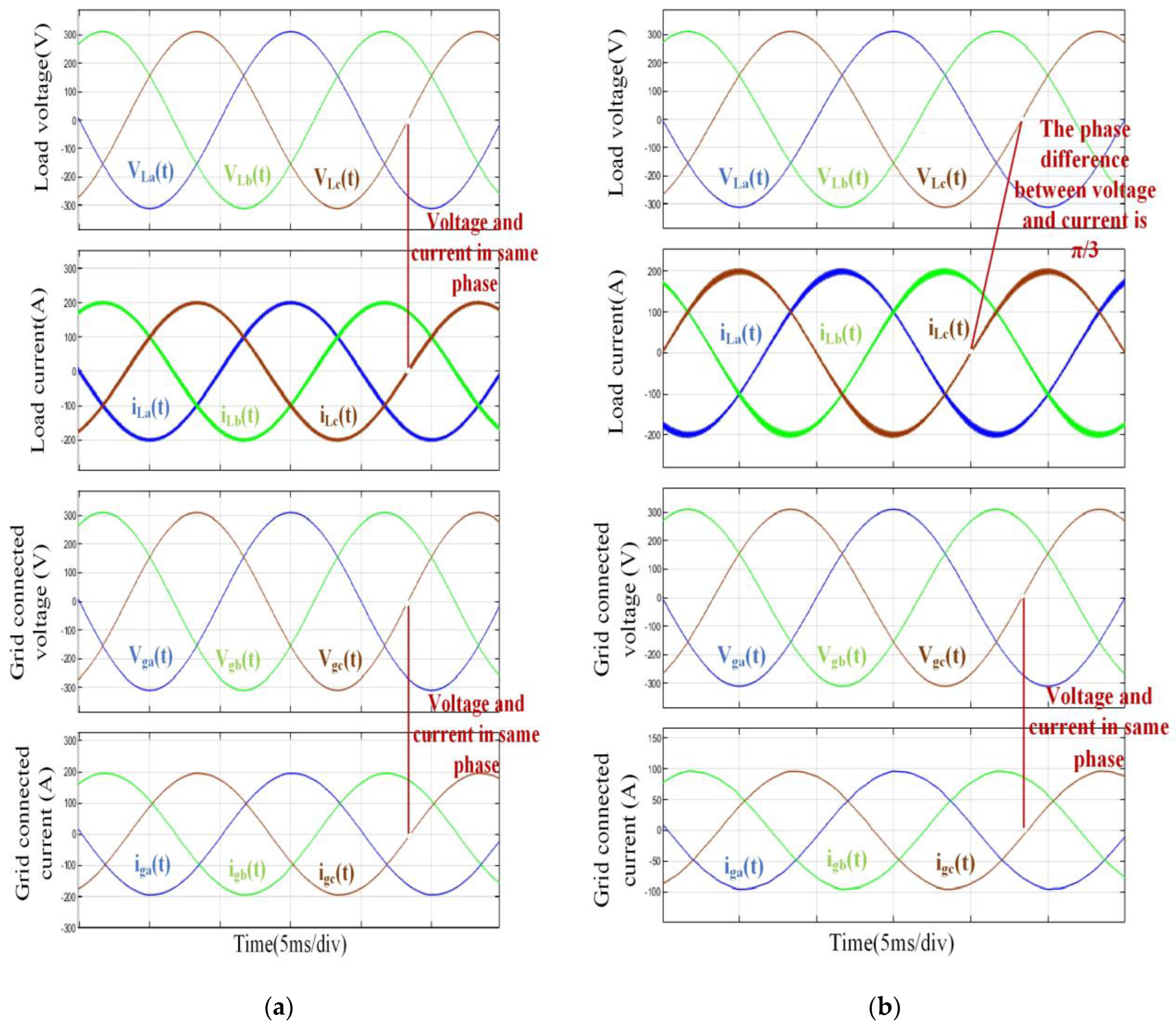
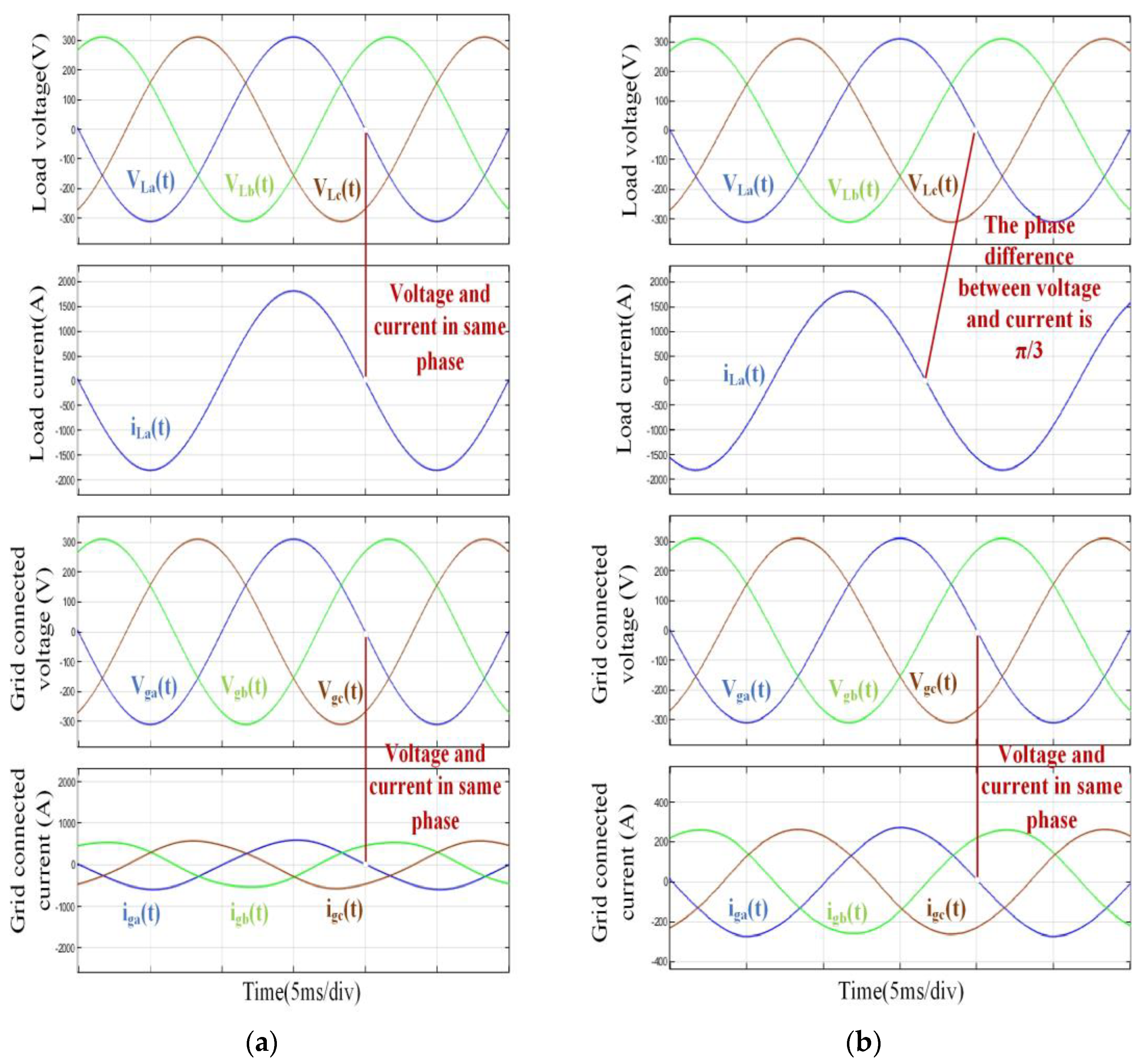
3.1. Results of the Simulation of Three-Phase Balanced Loads

When simulating three-phase balanced loads, the circuit model was constructed in MATLAB/Simulink, and specific experimental parameters were set as outlined in Table 1. According to China’s power grid voltage and frequency regulations, the effective value of the power supply voltage was set to 220 V and the frequency was set to 50 Hz. Based on the 200 kVA system voltage rating, the voltage value of the DC bus was set to 1000 V. The selection of parameters for the DC bus capacitor should meet the following requirements:
C > S/24frU2dc
In this equation, where S represents system capacity, f represents system frequency, Udc represents DC voltage, and r denotes the energy fluctuation range on the capacitor (2–5%).
The selection of parameters for the rectification side filter inductance should meet the following requirements:
L ≥ (U2dc − U2m)Ts/2Udc∆imax
where Udc represents DC voltage, Um represents the peak value of power phase voltage, Ts represents a switching cycle of IGBT, and ∆imax represents the maximum ripple of current harmonics.
The function of the inverter side inductance L1 is to limit the maximum value of the filtering inductance current ripple within a power frequency cycle, and based on this, the appropriate inverter side inductance is selected:
L1= UdcTsw/λc_L1I1
where Udc represents DC voltage, Tsw represents the switching cycle of PWM control, λc_L1 represents the current ripple coefficient of inductance, and I1 represents the fundamental effective value of inductance current.
After establishing the experimental model based on the provided parameter data, the simulated waveforms for three-phase balanced loads are obtained, as depicted in Figure 7a. Analyzing the image, from top to bottom, it shows the waveforms of the simulated load input voltages vlx(t) (where x represents a, b, and c), input currents, grid-connected voltage vgx(t), and current igx(t). Observing the waveforms in the image, it is evident that the input voltage and current are in phase, indicating a purely resistive simulated load. The input current amplitude meets the specified requirements, and the grid voltage and current are in phase, achieving unity power factor feeding. To simulate a capacitive three-phase balanced load, it is necessary to maintain the amplitude of the instruction current while modifying its phase to lead the grid voltage phase. The experimental results are illustrated in Figure 7b. Analyzing Figure 7b reveals that, in this case, the actual current in the load simulation converter leads the power source voltage by 60°. For the power source, this is equivalent to connecting a capacitive three-phase balanced load. In the grid-connected environment at the backend, the voltage and current are in phase, meeting the grid connection requirements. The experimental results demonstrate that the proposed circuit structure for simulating three-phase balanced loads can achieve load simulation effects and meet grid requirements. Moreover, it exhibits good simulation performance for both resistive and capacitive loads.

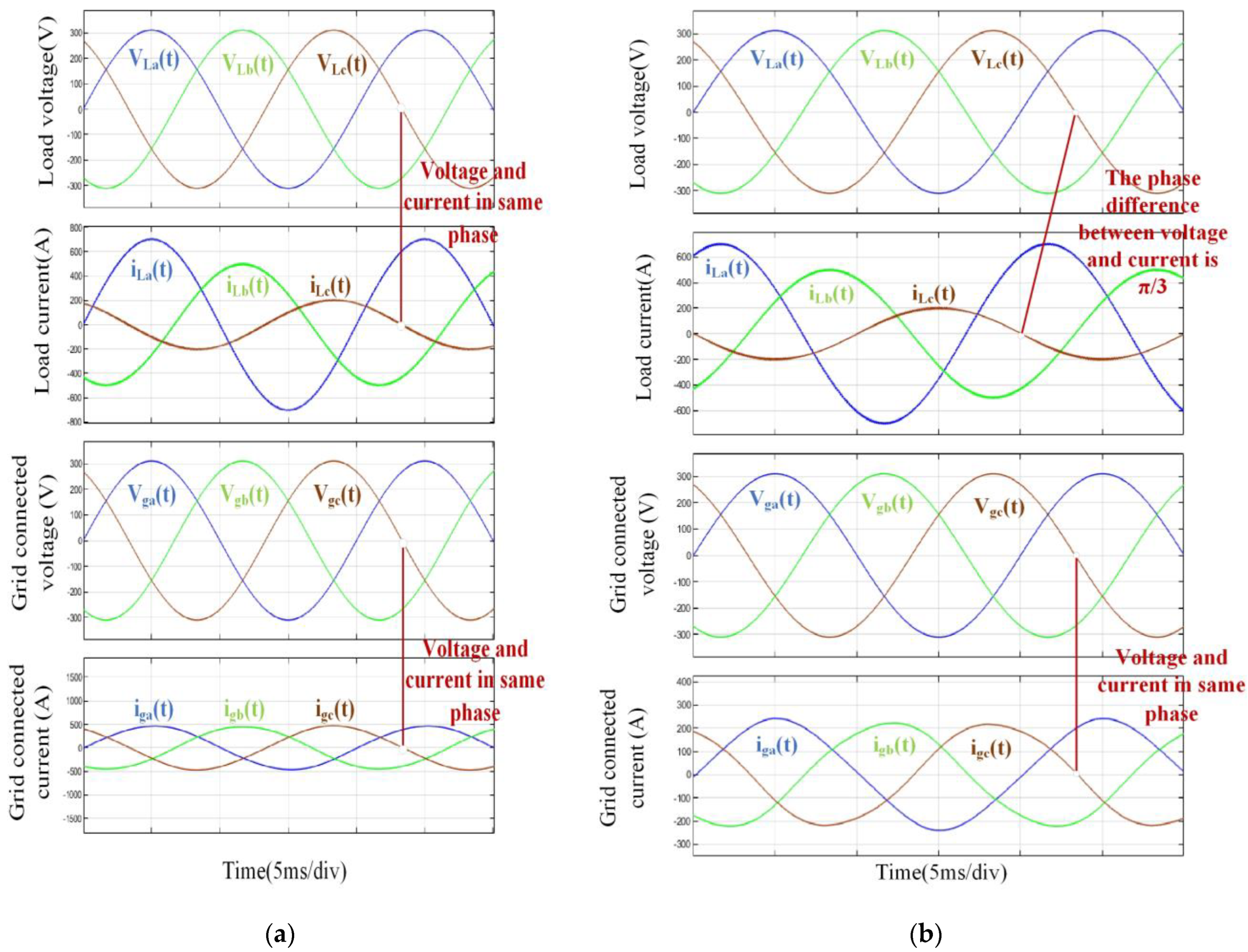
3.2. Results of the Simulation of Three-Phase Unbalanced Loads

When simulating three-phase unbalanced loads, the circuit model was constructed in MATLAB/Simulink, and specific experimental parameters were set as outlined in Table 2.
In this scenario, an instruction current generation module is utilized to produce three-phase unbalanced currents with unequal amplitudes and phase differences of 120° each. This is equivalent to connecting an unbalanced three-phase load to the test power source. Using PI control and SPWM control, the actual current in the circuit is adjusted to the specified values, thereby simulating an unbalanced three-phase resistive load. Peak values for the unbalanced three-phase currents are set to 700 A, 500 A, and 200 A, as illustrated in Figure 8a. Analysis of Figure 8a reveals that the voltage and current phases are identical, resembling a resistive load. The actual current in the circuit can reach the specified values, successfully accomplishing the task of simulating an unbalanced three-phase resistive load. The phase relationship between grid current and grid voltage is identical, achieving energy feedback.
For simulating an unbalanced three-phase capacitive load, the phase of the instruction current is adjusted to lead the source voltage phase by 60°. This is akin to connecting an unbalanced three-phase capacitive load to the tested power source. Experimental results, as depicted in Figure 8b, show that the current phase leads the source voltage phase by 60°, effectively simulating a capacitive load. Simultaneously, the phase relationship between grid current and grid voltage is identical, achieving energy feedback.

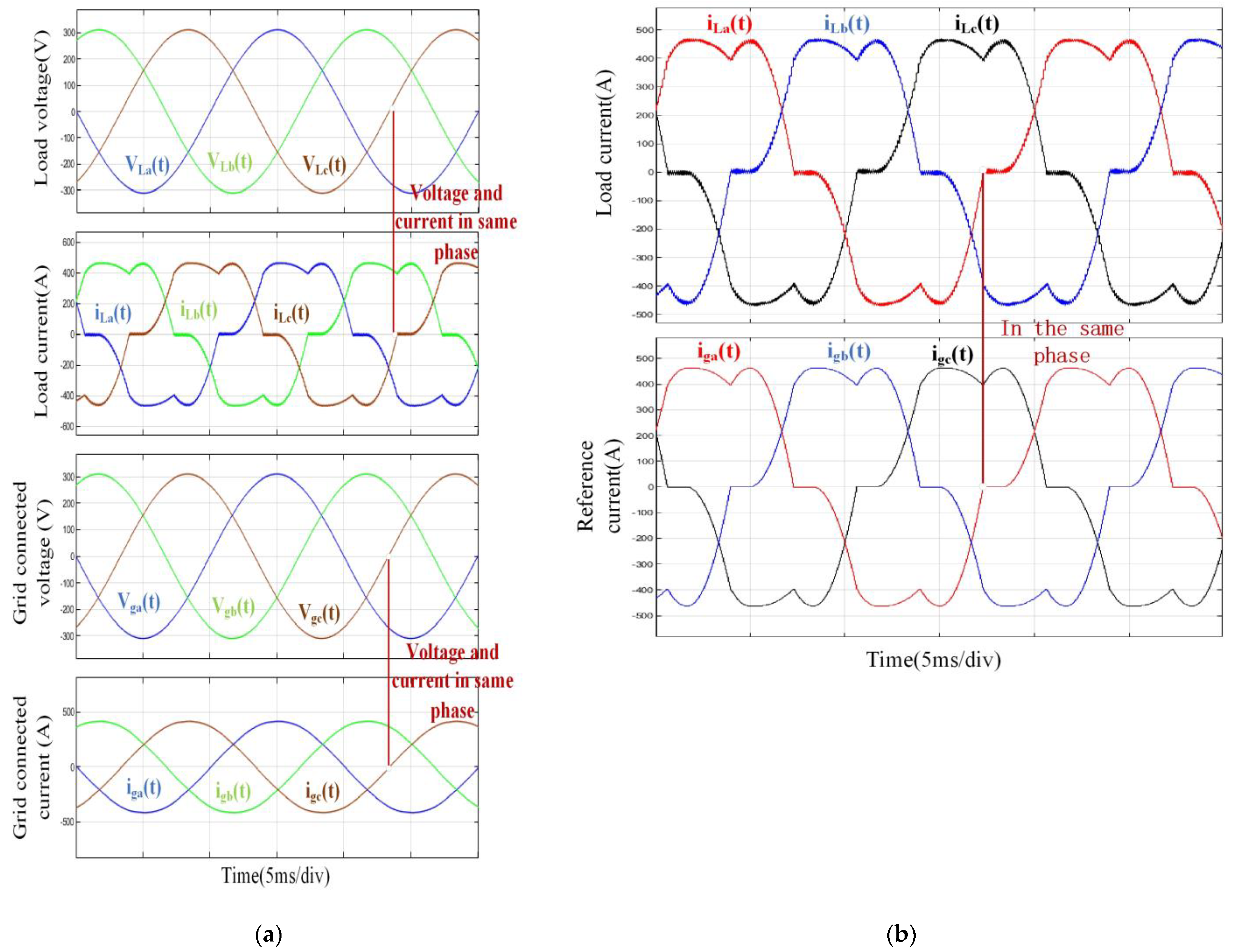
3.3. Results of the Simulation of Single-Phase Loads

When simulating three-phase unbalanced loads, the circuit model was constructed in MATLAB/Simulink, and specific experimental parameters were set as outlined in Table 3.
When simulating single-phase loads, arbitrarily selecting phase A as one side of the circuit and the fourth bridge arm as the other side, while keeping the other two phases normally closed, results in a front-end circuit structure resembling a single-phase half-bridge rectifier. Assuming the input current value of phase A is set to 1500 A, as depicted in Figure 9a, the waveform plots from top to bottom illustrate the waveforms of the input current and voltage, as well as the grid-side voltage and current. Analysis of the figure reveals that the input current and voltage are in phase and both reach the specified values. Furthermore, the grid voltage and current are in phase, achieving the desired energy feedback effect.
When simulating three-phase capacitive loads, a modification to the command current phase of phase A is sufficient, advancing it by 60° relative to the source voltage phase. As demonstrated in Figure 9b, under this condition, the phase difference between current and voltage is 60°, and the grid current remains in phase with the voltage, effectively achieving energy feedback.

3.4. Results of the Simulation of Non-Linear Loads

When simulating non-linear loads, the given current waveform, as depicted in Figure 10b, is analogous to connecting a nonlinear load to the test power source. Through the use of PI control and SPWM control, the actual current in the circuit is adjusted to the specified value, thereby achieving the simulation of three-phase unbalanced loads. As illustrated in Figure 10a, under these conditions, the phase relationship between voltage and current is identical, the actual current in the circuit attains the specified value, and the grid voltage remains in phase with the current, facilitating energy feedback.

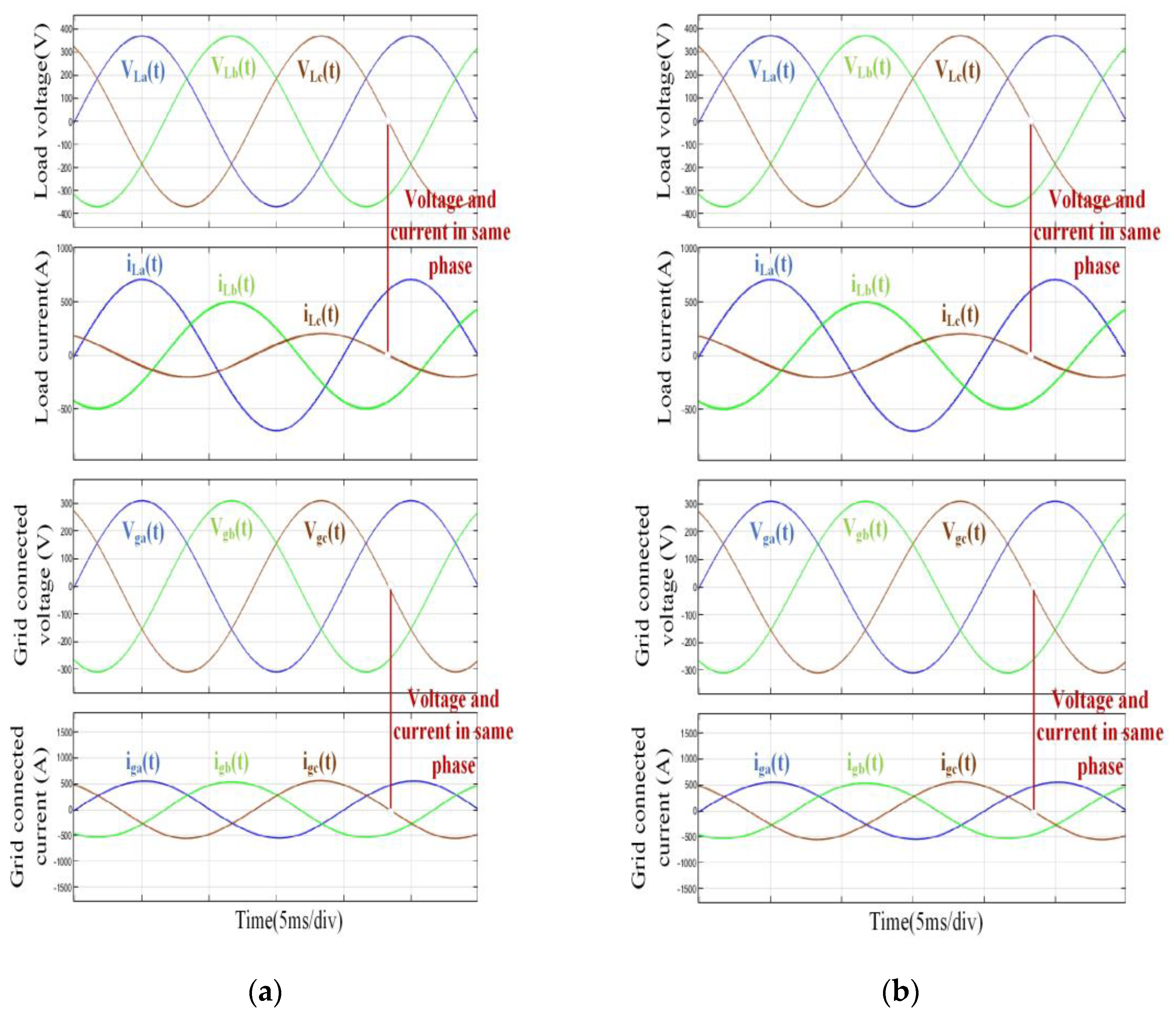
3.5. Results of the Simulation of Wide-Input Range Loads

When simulating three-phase unbalanced loads, the circuit model was constructed in MATLAB/Simulink, and specific experimental parameters were set as outlined in Table 4.
The input voltage of the circuit topology and test the circuit performance were adjusted when simulating three-phase unbalanced loads with input voltage amplitudes of 70 V and 370 V (20–120%). The three-phase input currents of 700 A, 500 A, and 200 A were selected, and the waveforms are shown in Figure 11a,b. When the input voltage is 70 V and 370 V, the input current can reach the given value, the voltage and current at the grid connection end are in phase, and the circuit function can still be achieved. When the input voltage is 70 V, the overall input power of the system is small, resulting in a poor grid connection waveform effect. Increasing the given current value properly can reduce the harmonic content in the grid connection current and achieve a better grid connection effect.

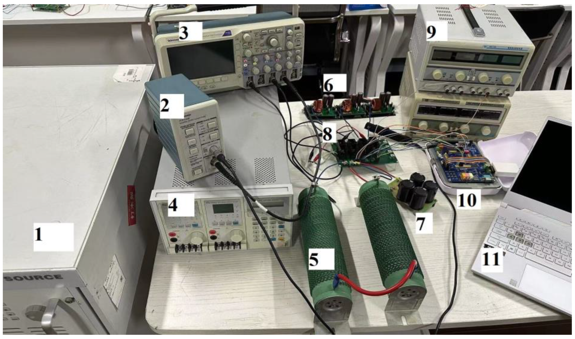
3.6. Results of Actual Test

The experiment environment of the actual test is shown in Figure 12.
The numbers in Figure 12 represent the following equipment:
  • Three-phase programmable AC power supply;
  • Current probe;
  • Oscilloscope;
  • Electronic load;
  • Power load;
  • Inductance;
  • DC-Link Capacitance;
  • Electronic load simulation part;
  • DC power supply;
  • DSP;
  • Upper control computer.
The actual experimental test environment was built as shown in Figure 12, and the waveform of the three-phase power supply voltage is shown in Figure 13.
According to China’s power grid voltage and frequency regulations, the effective value of the power supply voltage was set to 220 V and the frequency was set to 50 Hz. The subsequent experiments were set according to this standard for the power supply voltage.
As mentioned earlier, it is necessary to generate a three-phase unbalanced current to simulate three-phase unbalanced loads. Therefore, in physical testing, the generated three-phase unbalanced current is shown in Figure 14.
As shown in Table 4, the unbalanced phase currents of phase A, phase B, and phase C are set to 700 A, 500 A, and 200 A, respectively. By controlling the three-phase unbalanced current mentioned above, the effect of simulating three-phase unbalanced loads can be achieved.
Taking the simulation of a three-phase balanced load as an example, and due to the limitation of the number of channels in the oscilloscope, the current and voltage waveform of phase A is selected as the reference waveform, and the results of the actual test are shown in Figure 15, Figure 16 and Figure 17.
By analyzing Figure 15, it can be seen that when the circuit simulates a three-phase resistive balanced load, the voltage and current phases of phase A are the same and the values meet the standards. By analyzing Figure 16, it can be seen that when the circuit simulates a three-phase inductive balanced load, the voltage phase of phase A is ahead of the current phase of phase A, which is equivalent to connecting an inductive load to the power supply. By analyzing Figure 17, it can be seen that when the circuit simulates a three-phase capacitive balanced load, the current phase of phase A is ahead of the voltage phase of phase A, which is equivalent to connecting a capacitive load to the power supply.
The above actual test results are basically consistent with the simulation results, and it has been proven through actual test experiments that the proposed circuit structure has an excellent ability to simulate various kinds of loads.

4. Discussion

This article proposes an energy-feedback split-capacitor three-phase four-wire power electronic load capable of accommodating various load requirements. Subsequent analysis delineates its circuit topology when simulating three-phase balanced loads, three-phase unbalanced loads, single-phase loads, and nonlinear loads. The feasibility of the circuit structure is validated through simulation experiments. According to the simulation results, the proposed circuit structure can effectively simulate three-phase balanced loads, three-phase unbalanced loads, nonlinear loads, and single-phase loads. Using capacitive loads as an example demonstrates the circuit’s commendable performance with non-resistive loads.
When the input voltage effective value is 220 V and the bus voltage is 750 V, the circuit achieves a wide input range from 20% to 100% of the rated input voltage. However, beyond 110% of the rated input voltage, significant distortion occurs in the load simulation, challenging the original functionality of the circuit. Experimental observations reveal limitations in simulating large-range inductive–capacitive loads simultaneously with grid connection at a rated input voltage effective value of 220 V and a bus voltage of 750 V. To address this issue, increasing the rated bus voltage becomes imperative. Experiments show that setting the bus voltage to 850 V enables a wide input range from 20% to 110%, reducing the total harmonic distortion (THD) of the three-phase grid current to 4% during a 60° resistive–inductive load simulation. With the bus voltage set to 1000 V, a wide input range from 20% to 120% is achieved, and the THD of the three-phase grid current drops to 3.5% during the same 60° resistive–inductive load simulation. At bus voltages of 850 V and 1000 V, the input current waveform exhibits improved characteristics compared to 750 V. The final choice of bus voltage depends on practical usage and operational considerations. While 750 V fulfills the load simulation function, 850 V and 1000 V offer enhanced functionality at the cost of increased system expenditure.
This article addresses existing shortcomings in the field of energy-feedback AC electronic loads, particularly in research related to unbalanced and nonlinear loads, presenting a solution with broad practical applicability. The proposed circuit topology can be applied in load experiments for power supply testing. Compared to traditional load testing circuits, this circuit achieves multiple load simulations through a single structure, simplifying experimental conditions, enhancing equipment reliability, and reducing maintenance costs. Additionally, the circuit facilitates the recycling of electrical energy by feeding back test energy into the grid, minimizing energy wastage confined within its internal switching devices and circuits.
Future research endeavors may focus on the following aspects:
(1)
Constructing a prototype of a lower power rating to further validate the reliability of the circuit structure. The current study relied on Matlab/Simulink for simulation experiments; thus, creating a physical prototype involves calculating suitable device parameters, selecting components such as IGBTs, capacitors, and inductors, drawing schematic and PCB diagrams in Altium Designer, and designing protection circuits for devices like IGBTs. The operational results of the prototype will serve to validate the feasibility of the circuit structure and guide further optimizations based on practical issues.
(2)
Further optimizing the circuit structure: The prevalent structures of three-phase four-wire power electronic loads primarily involve either the split-capacitor structure described in this article or an alternative structure employing an additional set of IGBTs as the fourth bridge arm. Future research will experimentally and analytically investigate the structure utilizing IGBTs as the fourth bridge arm, comparing its advantages and disadvantages with the proposed split-capacitor structure in terms of control modes, circuit topology, simulation effects, and harmonic content within the circuit. This comparative analysis aims to identify the optimal design solution for the circuit.

5. Conclusions

Using a split capacitor as the fourth bridge arm in a three-phase four-wire power electronic load not only enables the simulation of balanced three-phase loads but also facilitates the simulation of unbalanced three-phase loads, single-phase loads, and non-linear loads with the same topology. Additionally, it allows for a wide range of voltage input amplitudes. This article analyzes the operational states of simulating balanced three-phase, unbalanced three-phase, and single-phase loads with a split capacitor in three-wire four-wire power electronic loads. The feasibility of this topology is verified via simulation and analysis.

Author Contributions

Conceptualization, B.L.; Methodology, S.S. and Q.H.; Writing—original draft, J.L. (Jiapeng Luo); Writing—review and editing, J.L. (Jianghua Lu) and Z.M.; Project administration, G.Z. All authors have read and agreed to the published version of the manuscript.

Funding

This research was funded by State Grid Corporation of China (No. 5200-202323140A-1-1-ZN) “Research and Engineering Demonstration of Key Technologies for Rapid Exchange and Ice Melting in Mountainous Agricultural Distribution Network Lines”.

Data Availability Statement

Data are contained within the article.

Conflicts of Interest

Author Shiyi Sun was employed by the State Key Laboratory of Disaster Prevention & Reduction for Power Grid. Author Qingjun Huang was employed by the Disaster Prevention and Reduction Center of Hunan Electric Power Co., LTD. of State Grid. The remaining authors declare that the research was conducted in the absence of any commercial or financial relationships that could be construed as a potential conflict of interest.

Abbreviations

AbbreviationsFull Name
IEEEInstitute of Electrical and Electronics Engineers
IEECInternational Electrotechnical Commission
UPSUninterruptible Power Supply
LSCLoad Simulation Converter
DBTDevices Be Test
EFCEnergy Feedback Converter
PWMPulse Width Modulation
SPWMSine Pulse Width Modulation
ACAlternating Current
DCDirect Current
IGBTInsulated Gate Bipolar Transistor
THDTotal Harmonic Distortion
PCBPrinted Circuit Board
PIProportional Integral
PLLPhase-Locked Loop
LCLInductance–Capacitance–Inductance

References

  1. Li, K. Research on High Power Supply Quality Control Scheme for Distribution Room. Electromech. Inf. 2023, 12–16. [Google Scholar]
  2. An, J.; Liu, X. Research on Energy Feedback AC Electronic Load for Power Supply Testing. New Technol. Electr. Energy 2021, 40, 66–72. [Google Scholar]
  3. Wu, C.; Zhu, Y.; Li, Y. Design of Grid Connected Circuit for Electronic Load. Ind. Control Comput. 2022, 35, 143–144+147. [Google Scholar]
  4. Liu, H.; Cai, H.; Liao, D.; Zhou, J. Passive backstepping control of AC electronic loads under unbalanced power grid. Power Electron. Technol. 2023, 57, 79–82+102. [Google Scholar]
  5. Chen, W.; Zeng, J. Research on Active Disturbance Rejection Control of Power Electronic Load Based on Improved LESO. Electr. Meas. Instrum. 2023, 1–15. [Google Scholar]
  6. Wu, J.; Zeng, Z.; Wu, X. Design of Energy Feedback Power Factor Adjustable Single Phase AC Electronic Load. Mod. Electron. Technol. 2023, 46, 160–166. [Google Scholar] [CrossRef]
  7. Pan, S.; Zhao, J.; Wang, X. Research on high-power AC electronic loads. Power Electron. Technol. 2006, 40, 97–100. [Google Scholar]
  8. Liu, C.; Ye, C.; Xu, Y.; Wu, J.; Zhao, W. Simulation Research on Energy Feedback Electronic Load Applied in Power Supply Testing. Power Technol. 2012, 10, 1546–1548. [Google Scholar]
  9. Wang, C.; Zou, X.; Xu, Y.; Zou, Y.; Zhang, Y.; Chen, W.; She, X.; Li, F. High power electronic loads using improved repetitive control. Chin. J. Electr. Eng. 2009, 12, 1–9. [Google Scholar]
  10. Cai, H.; Chen, L.; Wei, M.; Wei, D. An energy fed electronic load for testing the characteristics of photovoltaic power generation systems. J. Sol. Energy 2021. [Google Scholar] [CrossRef]
  11. Li, X. Research on Energy Feedback Electronic Load and Its Dynamic Characteristics. Master’s Thesis, Nanjing University of Aeronautics and Astronautics, Nanjing, China, 2023. [Google Scholar]
  12. Gupta, S.; Ruth, R. Load Bank Elimination for UPS Testing. In Proceedings of the IEEE Industry Applications Society Annual Meeting, Seattle, WA, USA, 7–12 October 1990. [Google Scholar]
  13. Chu, C.L.; Chen, J.F. Self-Load Bank for UPS Testing by Circulating Current Method. IEEE Proc. Electr. Power Appl. 1994, 141, 191–196. [Google Scholar] [CrossRef]
  14. O’Sullivan, G. A Power Supply Testing with the Power Recycler. IEEE Trans. Power Convers. 1992, 92, 228–235. [Google Scholar]
  15. Ayres, C.A.; Barbi, I. A family of converters for UPs production burn-in energy recovery. IEEE Trans. Power Electron. 1997, 12, 615–622. [Google Scholar] [CrossRef]
  16. Bonaldo, J.P.; Pomilio, J.A.; Vendrusculo, E.A. Power Equalization Techniques for Three-Phase VSI-Driven Single-Phase Ozone Generators. Ozone Sci. Eng. J. Int. Ozone Assoc. 2015, 37, 9–21. [Google Scholar] [CrossRef]
  17. Xu, L.; Fang, Y.; Liu, Y. Research on three-phase energy fed AC electronic loads based on dual PWM converters. Comput. Digit. Eng. 2020, 10, 2512–2518. [Google Scholar]
  18. Cai, H.; Mei, J.; Liao, D.; Tong, Y. Research on AC Energy Feedback DC Electronic Load. J. Cent. North Univ. Nat. Sci. Ed. 2017, 38, 364–372. [Google Scholar]
  19. Cao, Y. Research on the Control Scheme of Single-Phase Energy Feedback AC Electronic Load. Master’s Thesis, Shanghai Jiao Tong University, Shanghai, China, 2020. [Google Scholar]
  20. Deng, T. Design of Energy Feedback DC Electronic Load with Harmonic Compensation. Master’s Thesis, South China University of Technology, Guangzhou, China, 2020. [Google Scholar] [CrossRef]
  21. Heerdt, J.A.; Coutinho, D.F.; Mussa, S.A.; Heldwein, M.L. Control Strategy for Current Harmonic Programmed AC Active Electronic Power Loads. IEEE Trans. Ind. Electron. 2014, 61, 3810–3822. [Google Scholar] [CrossRef]
  22. Wu, Z.; Zou, X.; Huang, Q.; Zhang, Z.; Zou, Y. Research on three-phase power electronic load grid connected converter. Chin. J. Electr. Eng. 2010, 1–7. [Google Scholar] [CrossRef]
Figure 1. Topological structure of three-phase four-wire split capacitor power electronic load.
Energies 17 00119 g001
Figure 2. Circuit topology when simulating a three-phase balanced load.
Energies 17 00119 g002
Figure 3. Circuit topology when simulating three-phase unbalanced loads and non-linear loads.
Energies 17 00119 g003
Figure 4. The waveform of reference current when simulating non-linear loads.
Energies 17 00119 g004
Figure 5. The control strategy for the capacitor voltage equalization topology.
Energies 17 00119 g005
Figure 6. Circuit topology when simulating single-phase loads.
Energies 17 00119 g006
Figure 7. (a) The waveforms of simulating three-phase balanced resistive loads. (b) The waveforms of simulating three-phase balanced capacitive loads.
Energies 17 00119 g007
Figure 8. (a) The waveforms of simulating three-phase unbalanced resistive loads. (b) The waveforms of simulating three-phase unbalanced capacitive loads.
Energies 17 00119 g008
Figure 9. (a) The waveforms of simulating single-phase resistive loads. (b) The waveforms of simulating single-phase capacitive loads.
Energies 17 00119 g009
Figure 10. (a) The waveforms of simulating non-linear loads. (b) The comparison between the reference current and the actual current of simulating non-linear loads.
Energies 17 00119 g010
Figure 11. (a) The waveforms of simulating three-phase unbalanced loads with an input voltage of 370 V. (b) The waveforms of simulating three-phase unbalanced loads with an input voltage of 70 V.
Energies 17 00119 g011
Figure 12. The experiment environment of the actual test.
Energies 17 00119 g012
Figure 13. The waveform of the three-phase power supply voltage.
Energies 17 00119 g013
Figure 14. The waveform of the three-phase unbalanced current.
Energies 17 00119 g014
Figure 15. The waveform of the actual test of a three-phase balanced resistive load.
Energies 17 00119 g015
Figure 16. The waveform of the actual test of a three-phase balanced inductive load.
Energies 17 00119 g016
Figure 17. The waveform of the actual test of a three-phase balanced capacitive load.
Energies 17 00119 g017
Table 1. The specific experimental parameters of the simulation of three-phase balanced loads.
ParameterUnitValue
RMS voltage of the power source V220
Rectification side filter inductanceH700 × 10−6
DC bus voltageV1000
DC bus capacitorF10 × 10−3
Inverter side filter inductanceH500 × 10−6
Grid-connected side filter inductanceH250 × 10−6
LCL damping resistorR0.4
Frequency of the gridHz50
Peak value of three-phase balanced currentA200
Table 2. The specific experimental parameters of the simulation of three-phase unbalanced loads.
ParameterUnitValue
RMS voltage of the power source V220
Rectification side filter inductanceH700 × 10−6
DC bus voltageV1000
DC bus capacitorF10 × 10−3
Inverter side filter inductanceH500 × 10−6
Grid-connected side filter inductanceH250 × 10−6
LCL damping resistorR0.4
Frequency of the gridHz50
Peak value of Phase AA700
Peak value of Phase BA500
Peak value of Phase CA200
Table 3. The specific experimental parameters of the simulation of single-phase loads.
ParameterUnitValue
RMS voltage of the power source V220
Rectification side filter inductanceH700 × 10−6
DC bus voltageV1000
DC bus capacitorF10 × 10−3
Inverter side filter inductanceH500 × 10−6
Grid-connected side filter inductanceH250 × 10−6
LCL damping resistorR0.4
Frequency of the gridHz50
Peak value of Phase AA1500
Table 4. The specific experimental parameters of the simulation of wide-input range loads.
ParameterUnitValue
RMS voltage of the power source V220
Rectification side filter inductanceH700 × 10−6
DC bus voltageV1000
DC bus capacitorF10 × 10−3
Inverter side filter inductanceH500 × 10−6
Grid-connected side filter inductanceH250 × 10−6
LCL damping resistorR0.4
Frequency of the gridHz50
Peak value of Phase AA700
Peak value of Phase BA500
Peak value of Phase CA200
The voltage variation rangeV70–370
Disclaimer/Publisher’s Note: The statements, opinions and data contained in all publications are solely those of the individual author(s) and contributor(s) and not of MDPI and/or the editor(s). MDPI and/or the editor(s) disclaim responsibility for any injury to people or property resulting from any ideas, methods, instructions or products referred to in the content.

