Article

Quasi-Resonant Single-Switch High-Voltage-Gain DC-DC Converter with Coupled Inductor and Voltage Multiplier Cell

by
Giordano Luigi Schiavon
,
Eloi Agostini, Jr.
* and
Claudinor Bitencourt Nascimento
Department of Electrical Engineering, Federal University of Technology–Parana–UTFPR, Ponta Grossa 84017-220, PR, Brazil
*
Author to whom correspondence should be addressed.
Energies 2023, 16(9), 3874; https://doi.org/10.3390/en16093874
Submission received: 6 March 2023 / Revised: 26 April 2023 / Accepted: 27 April 2023 / Published: 3 May 2023
(This article belongs to the Special Issue Advanced DC-DC Power Converters and Switching Converters II)

Abstract

:
This paper introduces a quasi-resonant high-efficiency high-step-up DC–DC converter requiring a reduced number of components. The proposed circuit uses a coupled inductor associated with voltage multiplier cells to ensure high-voltage-gain operation without the necessity of an extremely high number of turns ratio. Quasi-resonant operation guarantees zero current switching (ZCS) for some diodes of the converter. A detailed steady-state analysis is carried out aiming at the adequate design of the circuit. Experimental results taken from the testing of a 400 W prototype operating in closed loop with an input voltage range of 25–48 V, output voltage of 400 V and switching frequency of 100 kHz validate the analysis carried out and demonstrate the feasibility of the proposed converter.

1. Introduction

Techniques associated with the generation of electrical energy have been improved to address the challenges associated with climate change and contribute to sustainable development. In this sense, production of electrical energy from renewable resources, such as wind, solar and biomass, is not an alternative anymore but a necessity [1,2]. Considering photovoltaic (PV) and fuel cell (FC) systems, the voltage levels are usually low and in the form of direct current (DC), diverging from the usual alternate current (AC) system that prevails in the distribution of electricity in most segments [3]. Thus, in order to adapt the voltage levels while taking into account technical and economic aspects, electronic energy processing is mandatory, from which low cost and high efficiency are expected. In this sense, high-step-up DC–DC converters are widely employed in applications where the primary energy source is characterized by a voltage level much lower than that required for the end use [4,5,6,7,8].
Providing energy to a DC distribution system or conditioning the voltage as an intermediate stage of a DC–AC conversion system are some applications of DC–DC converters. One of the main challenges in the use of such converters is to avoid expressive switching and conduction losses. Therefore, using circuits with a reduced number of components, featuring low-voltage stress on the semiconductors and with the ability of recycling the leakage energy are key to improving the overall system efficiency. However, achieving all these characteristics is not an easy task. One classic example is the boost converter, which is indeed a simple circuit but exhibits poor performance under high-voltage-gain conditions [9]. Addressing the limitations of the boost converter by the use of techniques to improve the voltage gain has been extensively investigated in the literature [10,11,12]. Among the several techniques discussed in [12], one can be highlighted: boost-based solutions using a single active switch, a single coupled inductor and voltage multiplier cells (VMCs), such as the boost-flyback and the boost associated with VMCs introduced in [13] and [14], respectively, in addition to other solutions recently reported in the literature [15,16,17,18,19]. In all these examples, voltage gain is dependent on the duty cycle (D) and on the number of turns ratio (n) of the coupled inductor. As a result, higher voltage conversion ratios can be achieved without extreme duty cycle values, and therefore a higher efficiency is expected, since conduction and switching losses are lower compared to the conventional step-up converters.
Converters employing a single active switch and reduced number of diodes and capacitors are usually not suited for applications where the power processed is higher than a few hundred watts. However, these circuits are interesting for processing energy from PV modules rated in the range of 200–600 W. In this sense, this work introduces a high-voltage-gain DC–DC converter based on the boost configuration using coupled inductor and voltage multiplier cells, as depicted in Figure 1. The key features of the proposed circuit that make it suitable for PV applications are: high efficiency; reduced number of components; low voltage stress on the semiconductors; and voltage distribution among the output capacitors. In addition, quasi-resonant characteristics guarantee ZCS operation for diodes D2 and D3, thus contributing to improving the system efficiency [20,21,22]. In addition, a high voltage conversion ratio can be achieved if compared with similar topologies, even though a relatively low number of turns ratio of the coupled inductor is adopted. Therefore, weight, volume and magnetic losses can be minimized.

2. Principle of Operation in Steady State

The proposed high-step-up DC–DC converter depicted in Figure 1 contains a VMC composed of the winding Ns of the coupled inductor associated with the pairs D2/C2 and D3/C3. Since this topology is able to impose high voltage levels on the capacitors, adopting a number of turns ratio close to one is possible without the need for overly high values of duty cycle. The steady-state analysis of the proposed converter is carried out for deriving a mathematical model that allows the proper choice of every component contained in the circuit. In this sense, the following assumptions are made:
  • All elements are considered ideal, except for the leakage inductance of the coupled inductor;
  • The voltage on the capacitors and the magnetizing current are assumed to be ripple free;
  • The analysis is carried out within one period of the switching frequency fs.
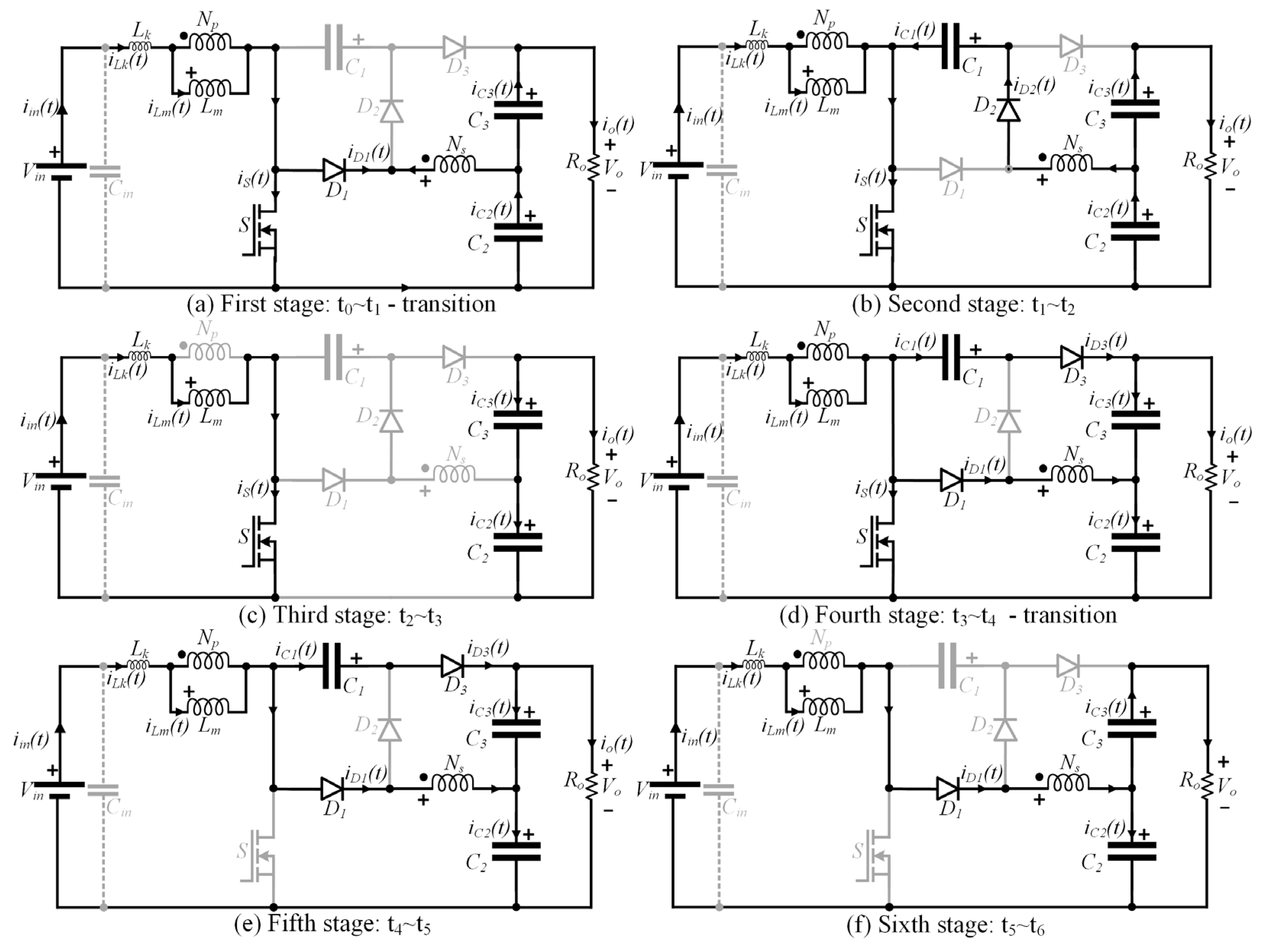
Six operating stages are verified from the analysis of the converter during one switching period, as depicted in Figure 2. From these six stages, only four are relevant in terms of the energy processed by the system. Hence, transition stages regarding the intervals ∆t1 and ∆t4 will be neglected from the mathematical analysis.
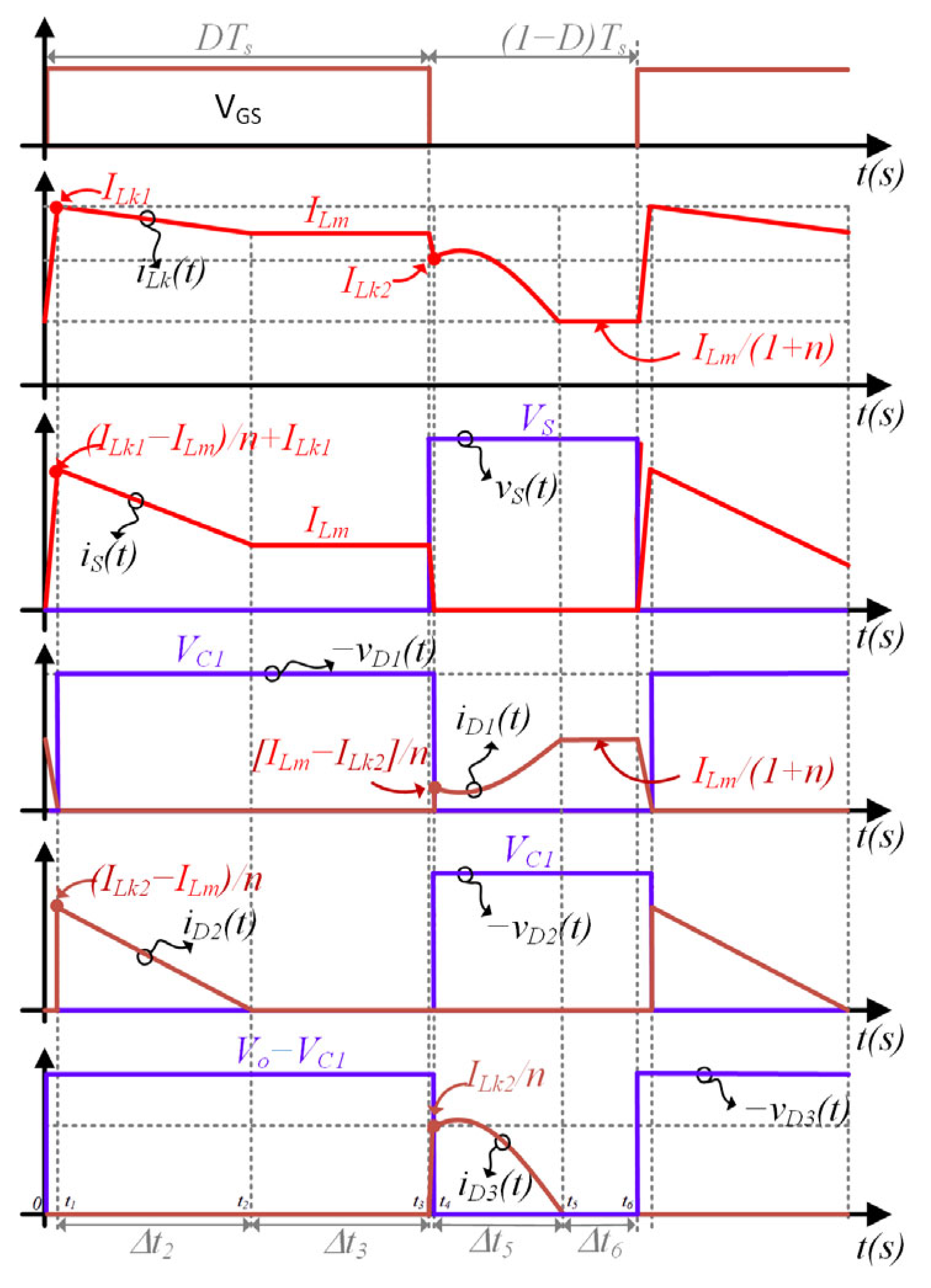
During the second and third stages, which correspond to the intervals ∆t2 and ∆t3, respectively, switch S is turned on, the magnetizing inductance Lm stores energy, and capacitors C2 and C3 provide energy that has been stored during the previous stages to the system. These intervals are characterized as linear stages, since resonance between the leakage inductance Lk and the capacitors contained in the circuit is not expressive. This operational condition is finished when S is turned off.
The fifth and sixth stages, defined by the intervals ∆t5 and ∆t6, occur when S remains in the off state. During these stages, energy stored in Lm is provided to the circuit. Resonance between Lk, C1 and C3 becomes expressive during the fifth stage. In this sense, if it is guaranteed that the resonant frequency is higher than the switching frequency, D2 operates with ZCS, thus contributing to increasing the system efficiency. It is noteworthy that the fifth stage plays a crucial role in defining the voltage gain of the converter. Regarding the sixth stage, the converter returns to a linear operating characteristic.
Figure 3 presents the main theoretical waveforms regarding the converter operation in steady state. As can be seen, an abrupt change in iLk occurs at the end of interval ∆t3, which is a simplifying assumption justified by the fact that the fourth stage corresponds to a very brief transition state, during which the energy processed can be neglected.

3. Mathematical Model

Fundamental information regarding the operation of the proposed converter can be extracted from the mathematical model of the circuit, such as the voltage conversion ratio and voltage stress on the semiconductor devices. Such knowledge is key to designing the circuit properly, aiming at reduced conduction and switching losses to ensure high-efficiency operation.

3.1. Steady-State Analysis

The proposed mathematical model takes into consideration the following definitions:
Δ t i = t i t i 1 ;     T s = 1 f s ;     n = N s N p ;     λ = L k L m ;     k = L m L k + L m ; M = V o V i n ;     M C 1 = V C 1 V i n ;     M C 2 = V C 2 V i n ;     M C 3 = V C 3 V i n ,
where i defines the interval of each stage beginning at ti−1 and ending at ti; Ts corresponds to the switching period; fs is the switching frequency; n defines the number of turns ratio of the coupled inductor; the factors λ and k relate the magnetizing and leakage inductances; and M, MC1, MC2 e MC3 correspond to the total and partial static gains of the circuit.
The fundamental equation for iLk(t) valid for the interval ∆t2 is given by (2).
I L m = I L k 1 + ( 1 M C 1 M C 2 n ) Δ t 2 λ L m V i n
The energy balance of the algebraic sum of the leakage and magnetizing inductances yields (3).
M C 2 + M C 3 M C 1 = 1 1 D
Equation (4) can be determined from the analysis of the equivalent circuit of the second stage depicted in Figure 2b.
M C 1 M C 2 = n k
As previously mentioned, resonance between Lk and the pair C1/C3 is expressive during the fifth stage of the proposed high-step-up DC–DC converter. Thus, the analysis of this stage can be carried out using the current and voltage on these elements.
Currents on C1 and C3 can be written in terms of iLk(t) as given by (5) and (6), respectively.
i C 1 ( t ) = I L m n ( 1 + n ) n i L k ( t )
i C 3 ( t ) = ( I L m n + I o ) + ( 1 + n ) n i L k ( t )
Equation (7) provides the voltage on the leakage inductance during the resonant stage.
v L k ( t ) = V i n V o + ( 1 + n ) n v C 1 ( t ) 1 n v C 3 ( t )
Differentiating (7) results in
d v L k ( t ) d t = ( 1 + n ) n d v C 1 ( t ) d t 1 n d v C 3 ( t ) d t .
Equation (8) can be rewritten in terms of the currents on C1 and C3, as given by
L k d 2 i L k ( t ) d t 2 = ( 1 + n ) n C 1 i C 1 ( t ) 1 n C 3 i C 3 ( t ) .
Substituting (5) and (6) into (9) results in the differential equation
L k C e q d 2 i L k ( t ) d t 2 + i L k ( t ) = A ,
where
C e q = n 2 ( 1 + n ) [ C 1 C 3 C 1 + ( 1 + n ) C 3 ] ,
A = 1 ( 1 + n ) [ I L m + n C 1 C 1 + ( 1 + n ) C 3 I o ] .
Applying the Laplace transform in (10) results in (13), which represents the current iLk(t) in the s domain.
I L k ( s ) = A ω o 2 s + s I L k 2 s 2 + ω o 2
where
ω o = 1 L k C e q .
At this time, current iLk(t) during the fifth stage can be determined by applying the inverse Laplace transform in (13), as given by (15). It is noteworthy that the resonant frequency fo must be higher than the switching frequency fs to guarantee ZCS for D3.
i L k ( t ) = ( V o 1 + n D 1 D V i n V C 3 ) sin ( ω o t ) n L k ω o + A + ( I L k 2 A ) cos ( ω o t )
Differentiating (15) and multiplying the result by Lk provides the value of vLk, as given by
v L k ( t ) = 1 n [ V o V C 3 ( 1 + n D ) V i n ( 1 D ) ] cos ( ω o t ) + ω o L k ( I L k 3 A ) sin ( ω o t ) .
Assuming that at t = 0 vLk is approximately equal to 0, one can derive the partial static gain MC3 as
M C 3 = M 1 + n D 1 D .
The circuit analysis reveals that the static gain M corresponds to the sum of MC2 and MC3, as given by (18), which allows computing MC2 as (19).
M = M C 2 + M C 3
M C 2 = 1 + n D 1 D
Substituting (19) into (4) yields the value of MC1 given by
M C 1 = 1 + n 1 D + n   k   .
Lastly, the total voltage gain M can be determined by substituting (4) and (17) into (3).
M = 2 + n   D 1 D + n   k
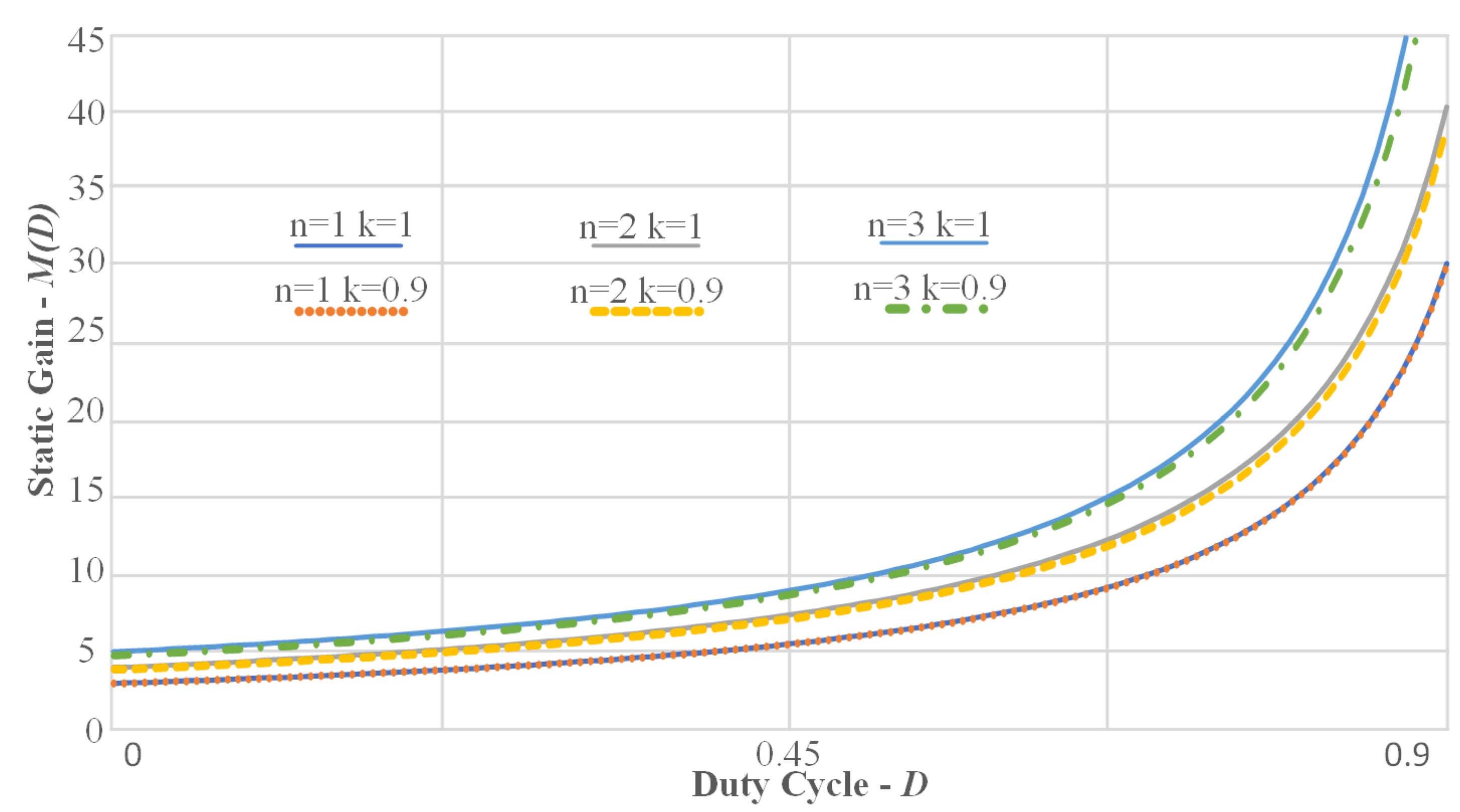
It can be concluded from (21) that lower values of k yield lower voltage conversion ratios. On the other hand, if the leakage inductance is low, the factor k tends toward one, and consequently the voltage gain converges to an ideal operating condition. In addition, the impact of k is minimized when the number of turns ratio is lower.
Figure 4 presents several curves of the voltage gain M as a function of the duty cycle D for different values of n and k. For the condition n = 1, it is evident that the influence of k is neglectable. On the other hand, as n increases and k decreases, the voltage gain deviates from the ideal case.
The unknowns ILk1 and ILk2, as well as the intervals ∆t2 and ∆t5, can be determined using (2) and (15) along with the average current on D2 e D3, which in turn are equivalent to the average output current Io and are given by (22) and (23), respectively.
1 T s 0 Δ t 5 i C 1 ( t )   d t = I o
( I L k 1 I L m 2 n ) Δ t 2 T s = I o
To complete the mathematical model of the proposed converter, it is fundamental that the equations defining the values of C1, C2 and C3, the magnetizing inductance Lm and the voltage stress on the semiconductor devices are derived.
Based on the operating stages depicted in Figure 2, it is possible to conclude that the values of C1, C2 and C3 can be determined by (24), (25) and (26), respectively. However, C1 and C3 can also be determined using the resonance criterion given by (14) and (11), which is used in this work to calculate these capacitances.
C 1 = 1 Δ V C 1 0 Δ t 5 i C 1 ( t )   d t
C 2 = 1 Δ V C 2 [ 0 Δ t 5 ( i L k ( t ) n I o ) d t + I L m 1 + n Δ t 6 ]
C 3 = D T s I o Δ V C 3
where ∆VC1, ∆VC2, ∆VC3 are the voltage ripples on C1, C2 and C3, respectively.
The magnetizing inductance Lm can be computed using
L m = ( 1 D ) ( V C 1 V C 3 ) T s n Δ I L m ,
where ∆ILm is the current ripple on Lm.
It can be concluded from Figure 2b,e that the voltage stress on D1 and D2 is equal to the voltage on C1 given by (20).
V D 1 = V D 2 = ( 1 + n 1 D + n   k ) V i n
The voltage stress on S and D3 can be determined from the analysis of the second and fifth operating stages, resulting in
V S = V D 3 = V i n 1 D .
The proposed converter can be designed and validated in the laboratory based on the mathematical analysis detailed so far. Moreover, a detailed efficiency analysis can be performed to determine the advantages of the proposed circuit for the intended applications, especially PV and FC systems.

3.2. Control Strategy

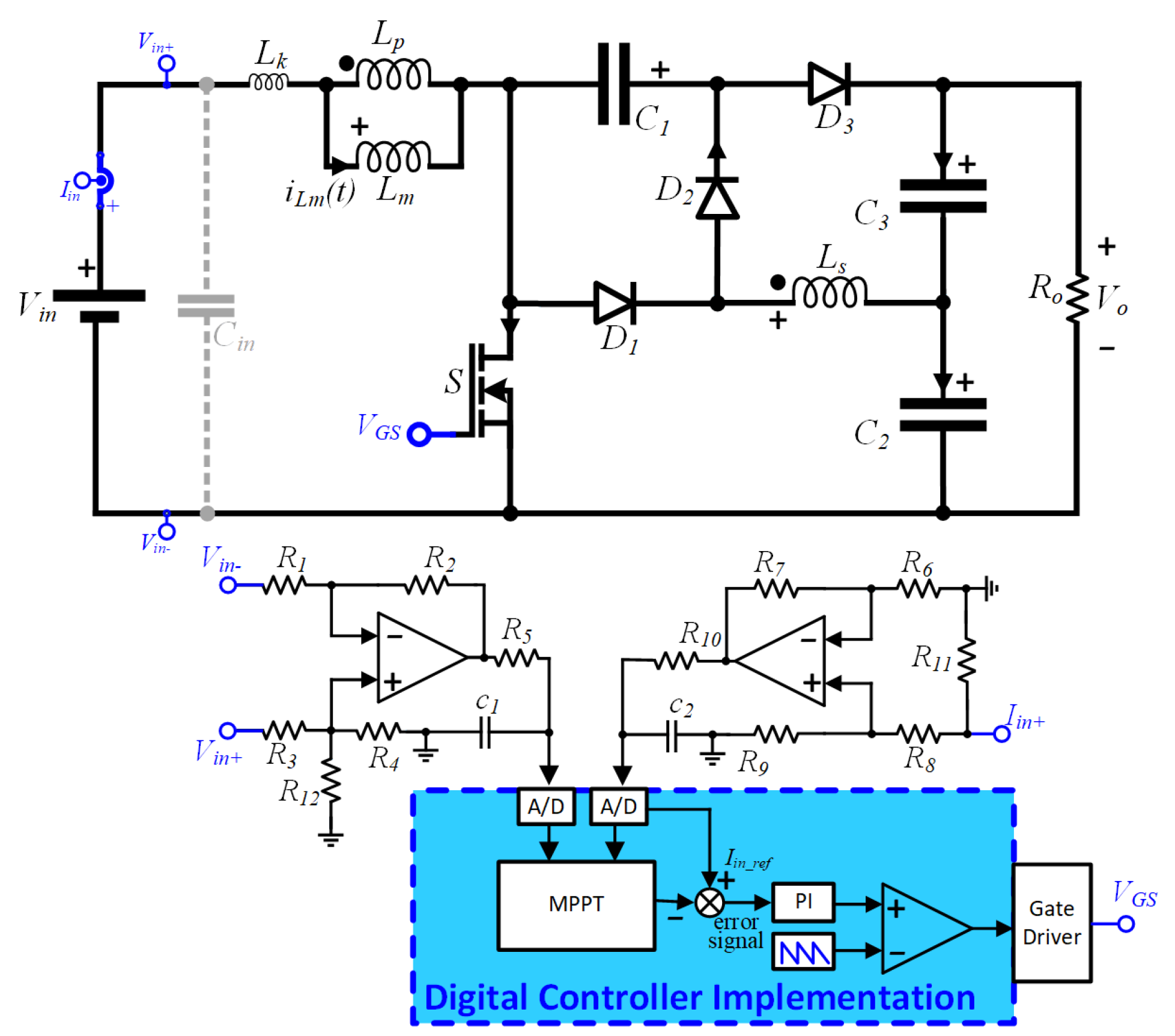
As known, PV and FC systems require a proper control system to ensure maximum power point tracking (MPPT) operation. In such a system, the DC–DC converter stage is directly responsible for MPPT realization by means of controlling the input voltage or current. In this paper, a control strategy aiming at controlling the input current is adopted, in accordance with the schematic depicted in Figure 5.
In the proposed scheme, input voltage and current are measured using the digital signal processor TMS320F28377S, in which an input current compensator is implemented. First-order filters with a cutoff frequency of 1 kHz are used for signal conditioning and analog-to-digital conversion is performed with a sampling frequency equal to 100 kHz. In this work, a proportional–integral (PI) controller with proportional and integral gains of 0.005 and 15, respectively, is used to adjust the input current, which in turn allows MPPT to be realized. It is noteworthy that the small-signal analysis of the proposed circuit is very extensive due to the high number of operating stages and quasi-resonant operation, and therefore it will not be detailed in this paper. Nevertheless, closed-loop operation will be investigated to demonstrate the suitability of the proposed converter for PV and FC applications.

4. Experimental Results

The experimental verification of the proposed converter is carried out using a 400 W prototype designed in consideration of the specifications shown in Table 1.
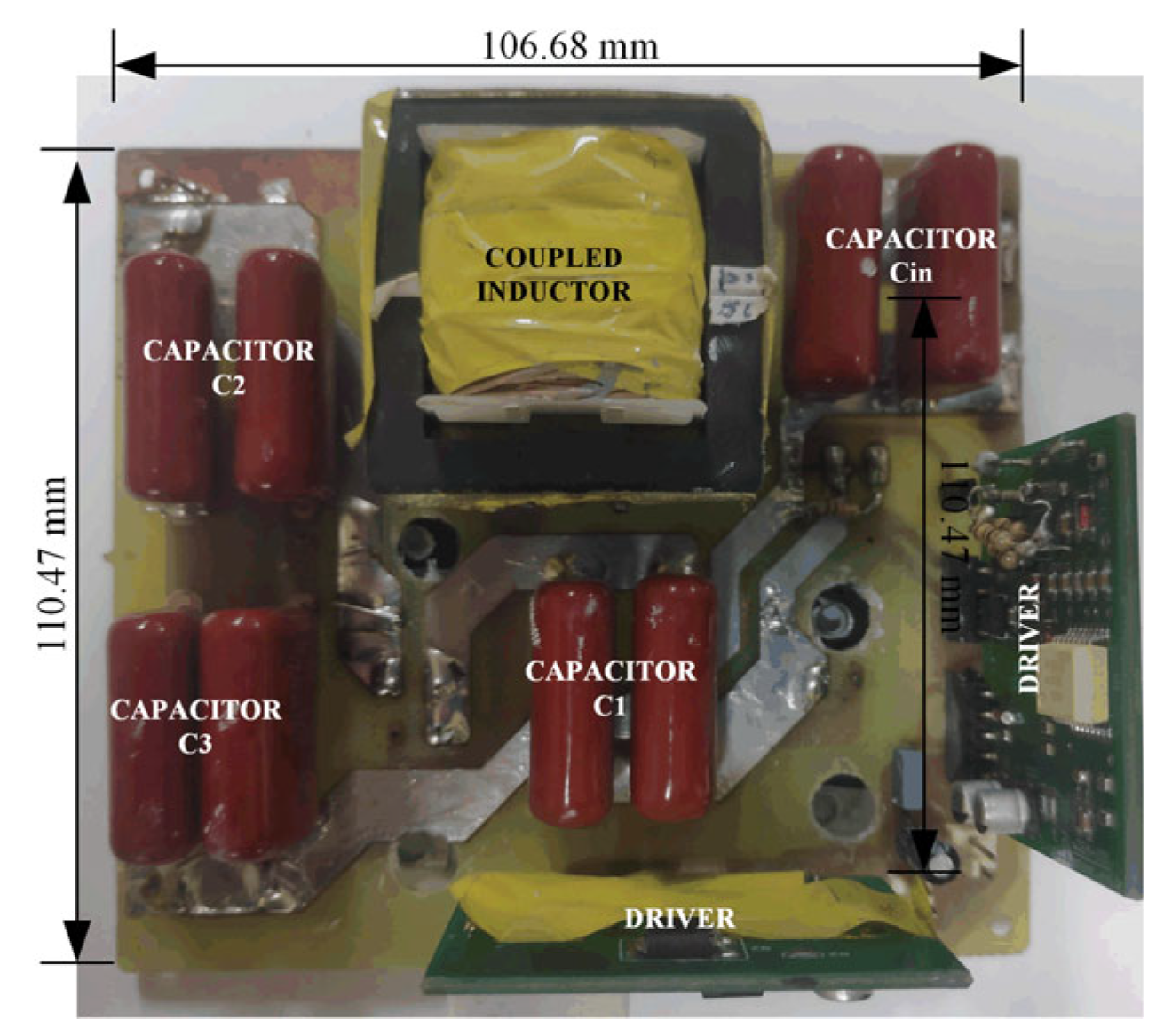
As previously mentioned, the resonance criterion was adopted to determine the capacitances C1, C2 and C3. In this sense, the leakage inductance was initially estimated as Lk = 2 µH. Next, Equation (14) was used to determine Ceq, which in turn can be used to calculate C1 and C3 using (11). It is noteworthy that fo was chosen to be higher than fs, and thus ZCS is guaranteed for D3. Based on the knowledge that the most expressive resonance occurs in the fifth stage, which corresponds to the interval ∆t5 that can last as long as (1 − D) ·Ts, it was decided that fo = 1.6·fs. The main results obtained from the design of the proposed converter are listed in Table 2 and a picture of the prototype is shown in Figure 6.
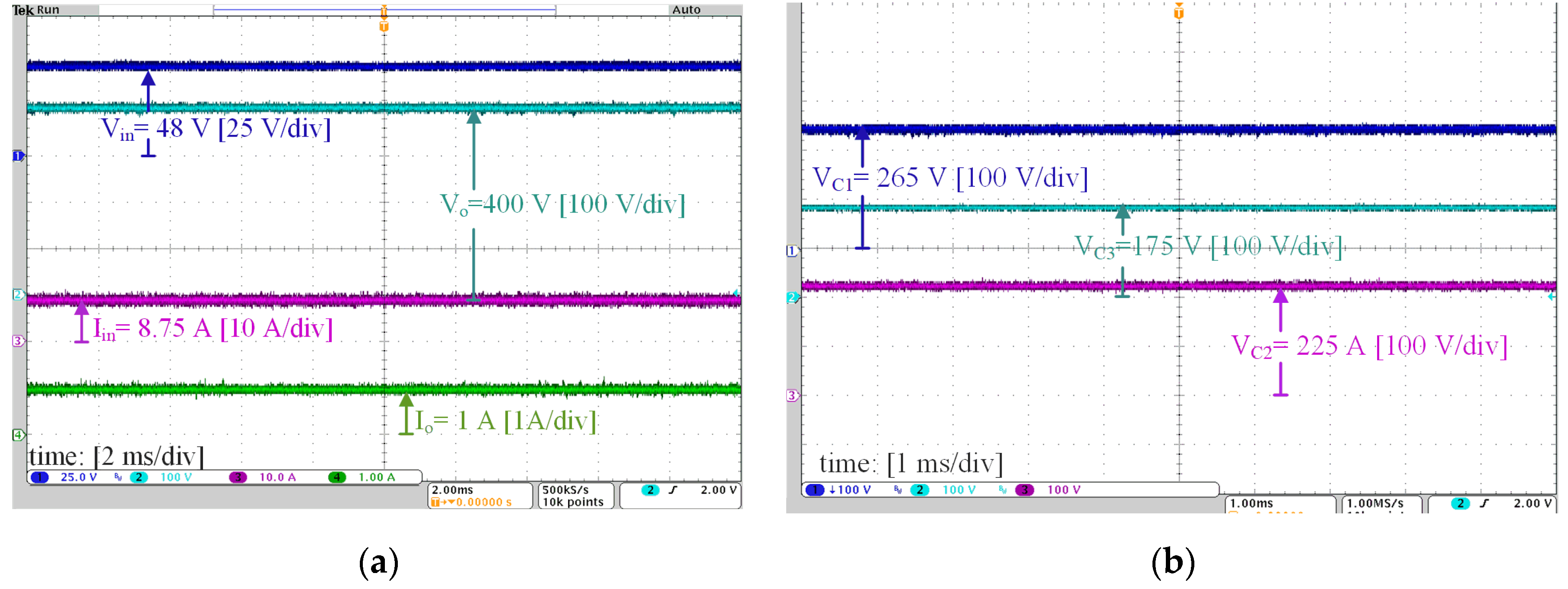
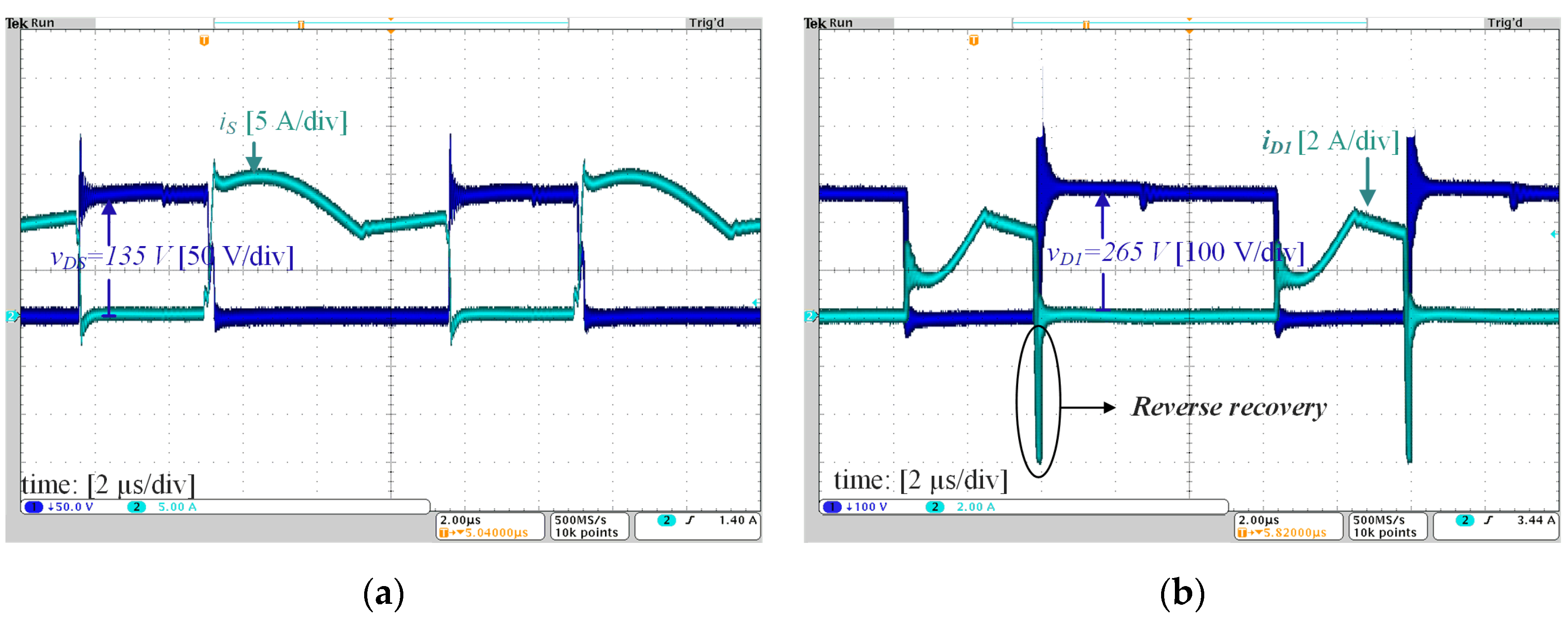
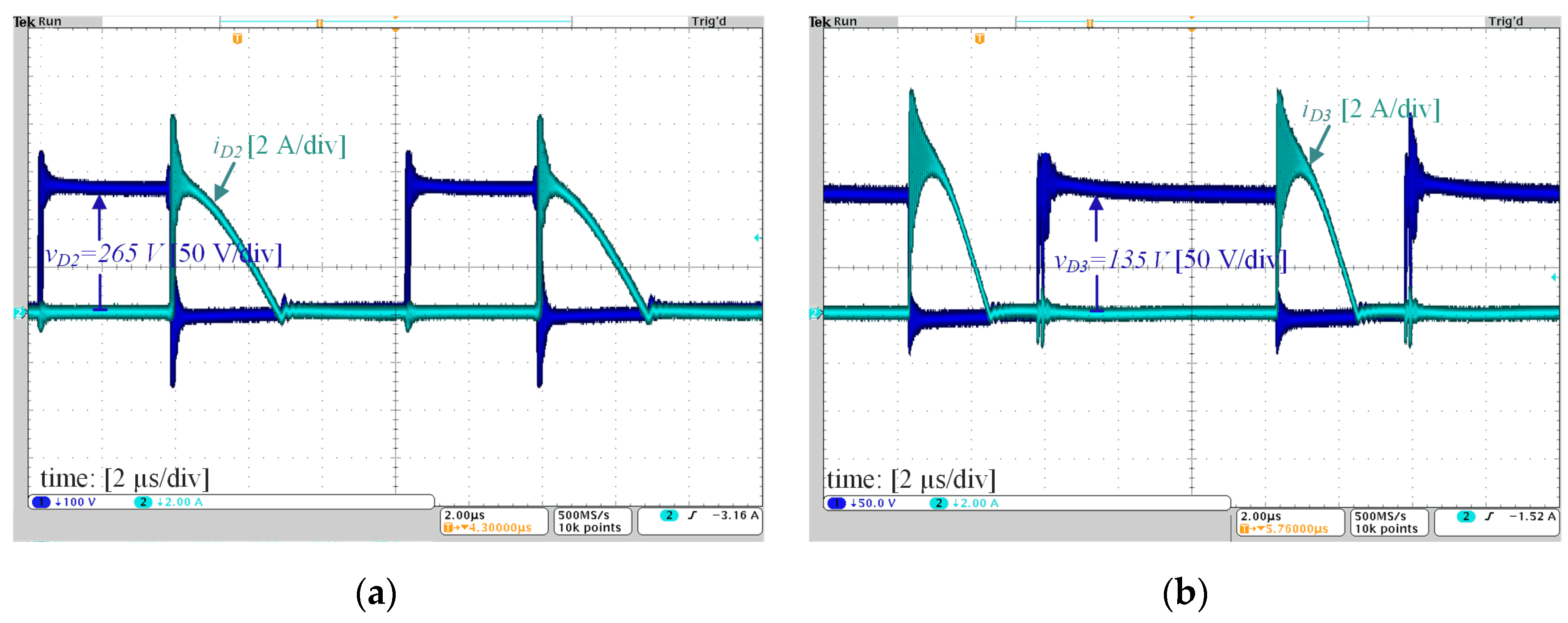
Voltage and current at the input and output are depicted in Figure 7a. Input current was measured before the decoupling capacitor Cin, resulting in a filtered low-current ripple waveform. Figure 7b shows the voltage on capacitors C1, C2 and C3. The results are in accordance with the theoretical predictions given by (20), (19) and (17), respectively. The voltage and current on the switch S are depicted in Figure 8a. The waveforms indicate dissipative commutation, but it is evident that the drain-to-source voltage is much lower than the output voltage. Consequently, a low-RDSon MOSFET can be used, thus minimizing the conduction and switching losses on this device. Voltage and current on D1, D2 and D3 are shown in Figure 8b and Figure 9a,b, respectively. These results confirm that the commutation of D1 is dissipative, as a considerable reverse recovery current is observed. However, this reverse current does not appear on the switch current (c.f., Figure 8a), and therefore its impact on the switching losses becomes limited. It can be also verified that D2 and D3 operate with ZCS as a result of the resonant characteristic of the current on these devices. The most expressive resonance occurring during the fifth stage and predicted in the theoretical analysis is evident on the waveform of the current on D3. The measured resonant frequency was approximately 190 kHz, deviating from the 160 kHz (1.6·fs) defined in Table 1. This difference was expected, because the actual leakage inductance of the coupled inductor measured in laboratory was Lk = 1.45 µH, a value lower than the 2 µH estimated during design.
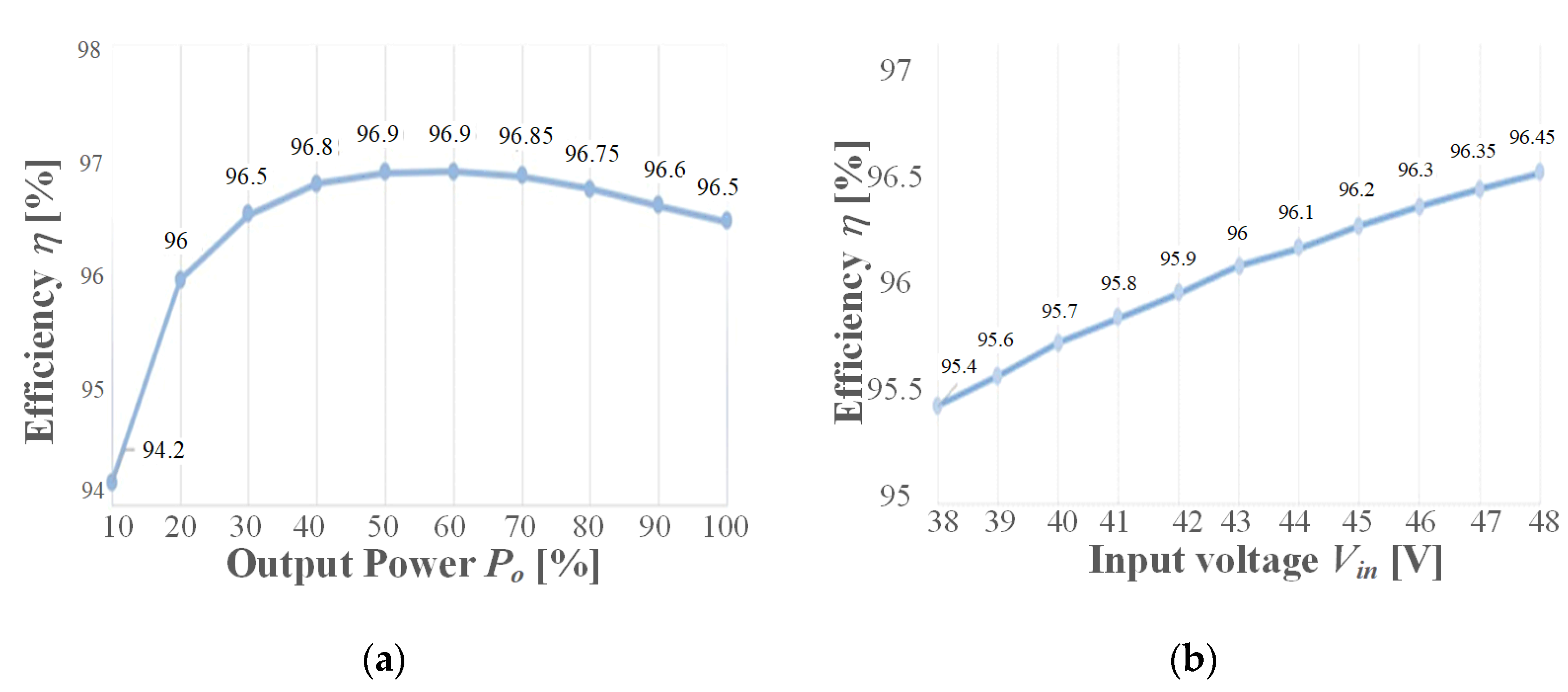
Efficiency measurements were taken using the power precision analyzer Yokogawa WT500 and are presented in Figure 10. Tests under three different situations were performed to create conditions in accordance with the specifications of 250–400 W solar modules. Figure 10a presents the efficiency curve versus output power considering input and output voltages fixed at 48 V and 400 V, respectively. A maximum efficiency of 96.9% was measured at 60% of rated output power, while the full-load efficiency was 96.46%. Efficiency versus input voltage variation, maintaining the output power fixed at 400 W, is shown in Figure 10b. It is evident that the efficiency is considerably reduced at low input voltage due to increased current levels. A more realistic situation is when the output power decreases as the input voltage is reduced. Figure 10c shows the efficiency versus input voltage considering an output power variation of 250–400 W. Although an efficiency reduction is also observed as the input voltage decreases, the impact is not as severe as that verified in the test with Po fixed at 400 W.
Finally, closed-loop operation with the output voltage fixed at 400 V is demonstrated in Figure 11. Steps in the input current reference from 4.25 A to 8.75 A and from 8.75 A to 4.25 A were applied, and the response demonstrates the proper operation of the converter using the control strategy depicted in Figure 5. In the tests, the output voltage was regulated at 400 V by the electronic load NHR9430 operating in the constant voltage mode to emulate the behavior of a grid-tied inverter stage. It is also noteworthy that the input current was measured before the filter capacitor Cin, and hence its ripple is lower than the theoretical prediction depicted in the waveform of iLk (c.f., Figure 3).

Comparative Analysis

The proposed converter is compared with the high-voltage-gain topologies proposed in [5,6,13,14,15,16,17], as summarized in Table 3. In this comparative analysis, only circuits containing a single active switch and one coupled inductor with two windings are considered. In addition, it is assumed that the leakage inductance of the coupled inductor is much smaller than its magnetizing inductance. As can be concluded from Table 3, both the voltage gain M and the voltage stresses on the semiconductors are usually related to the number of diodes and capacitors contained in the circuits. The circuits proposed in [5,13] contain only two diodes and two capacitors, although in [5] the voltage stress on the switch and on the diode D2 is equal to the entire output voltage level. As a result, higher conduction and switching losses are expected. The converters introduced in [15,17] exhibit the higher voltage gains, but more diodes and capacitors are employed. The boost-flyback converter proposed in [13] presents the lower voltage conversion ratio, and also requires the use of an auxiliar snubber to prevent potentially destructive voltage spikes on D3. As a consequence, if the same duty cycle is adopted, a higher number of turns ratio is required to reach the same voltage gain, and therefore weight and cost of the coupled inductor are also increased. It is also noteworthy that the snubber required for proper operation increases the losses of the circuit, which has an impact on the overall system efficiency. The converters proposed in [6,14,16] present similar constructive and operational characteristics. The highest efficiencies are verified in the proposed converter and in the circuit introduced in [6]. However, the proposed converter has a higher voltage gain and was tested with a higher switching frequency.

5. Conclusions

A novel high-step-up DC–DC converter based on the boost converter employing one coupled inductor and voltage multiplier cells was proposed in this paper. The circuit contains a single active switch, three diodes and three capacitors, and is capable of achieving a high conversion ratio even when a low number of turns ratio is adopted. It was demonstrated that using a low number of turns ratio minimizes the influence of the leakage inductance on the voltage gain. In addition, the resonant characteristic of the circuit provides ZCS operation for two of its diodes, thus reducing the switching losses and improving the system efficiency. A detailed efficiency analysis was performed in the laboratory, and the results demonstrate that the proposed converter is a viable solution for applications with a power rating on the order of a few hundred watts, since it is capable of providing high voltage gain with a reduced number of components.

Author Contributions

Conceptualization, G.L.S. and C.B.N.; software, G.L.S.; validation, G.L.S., E.A.J. and C.B.N.; formal analysis, G.L.S., E.A.J. and C.B.N.; investigation, G.L.S.; data curation, G.L.S.; writing—original draft preparation, C.B.N.; writing—review and editing, E.A.J.; supervision, C.B.N.; project administration, C.B.N.; funding acquisition, E.A.J. and C.B.N. All authors have read and agreed to the published version of the manuscript.

Funding

This research was funded in part by the Coordination for the Improvement of Higher Education Personnel (CAPES)–Financing Code 001.

Data Availability Statement

No new data were created in this work.

Conflicts of Interest

The authors declare no conflict of interest.

Nomenclature

Abbreviations
ACAlternate Current
DCDirect Current
FCFuel Cell
MPPTMaximum Power Point Tracking
PIProportional–Integral
PVPhotovoltaic
VMCVoltage Multiplier Cell
ZCSZero Current Switching
Symbols
ILmCurrent ripple on Lm
tiInterval of the i-th operating stage
VC1, ∆VC2, ∆VC3Voltage ripple on C1, C2 and C3
λInductance factor 1
ωoResonant angular frequency
ASimplifying term
Ceq1Equivalent capacitance
DDuty cycle
foResonant frequency
fsSwitching frequency
iC1, iC2, iC3Instantaneous current on C1, C2 and C3
iinInstantaneous input current
iLkInstantaneous current on Lk
ILk(s)Laplace transform of iLk
ILk1Current on Lk at t = t1
ILk2Current on Lk at t = t4
ILmAverage value of the current on Lm
IoAverage value of the output current
kInductance factor 2
MVoltage gain
MC1, MC2, MC3Partial voltage gains on C1, C2 and C3
nNumber of turns ratio
RDSonOn-resistance of the MOSFET
TsSwitching period
vC1, vC2, vC3Instantaneous voltage on C1, C2 and C3
VD1, VD2, VD3Maximum voltage stress on diodes D1, D2 and D3
VinInput voltage
VGSGate-to-source voltage on the MOSFET
vLkInstantaneous voltage on Lk
VoOutput voltage
VSMaximum voltage stress on switch S

References

  1. Shubbak, M.H. Advances in solar photovoltaics: Technology review and patent trends. Renew. Sustain. Energy Rev. 2019, 115, 109383. [Google Scholar] [CrossRef]
  2. Li, Z.; Ma, T.; Yang, H.; Lu, L.; Wang, R. Transparent and colored solar photovoltaics for building integration. Solar RRL 2021, 5, 2000614. [Google Scholar] [CrossRef]
  3. Premkumar, M.; Subramaniam, U.; Haes Alhelou, H.; Siano, P. Design and Development of Non-Isolated Modified SEPIC DC-DC Converter Topology for High-Step-Up Applications: Investigation and Hardware Implementation. Energies 2020, 13, 3960. [Google Scholar] [CrossRef]
  4. Zheng, Y.; Smedley, K.M. Analysis and design of a single-switch high step-up coupled-inductor boost converter. IEEE Trans. Power Electron. 2020, 35, 535–545. [Google Scholar] [CrossRef]
  5. Hass, E.S.; Nascimento, C.B. A simple self-clamped high step-up DC-DC converter employing coupled inductor. Braz. Power Electron. J. 2019, 24, 204–213. [Google Scholar]
  6. Rosas, I.P.; Agostini, E.; Nascimento, C.B. Single-switch high-step-up DC-DC converter employing coupled inductor and voltage multiplier cell. IEEE Access 2022, 10, 82626–82635. [Google Scholar] [CrossRef]
  7. Wu, Y.-E.; Wu, Y.-L. Design and Implementation of a High Efficiency, Low Component Voltage Stress, Single-Switch High Step-Up Voltage Converter for Vehicular Green Energy Systems. Energies 2016, 9, 772. [Google Scholar] [CrossRef]
  8. Rahimi, T.; Islam, M.R.; Gholizadeh, H.; Mahdizadeh, S.; Afjei, E. Design and Implementation of a High Step-Up DC-DC Converter Based on the Conventional Boost and Buck-Boost Converters with High Value of the Efficiency Suitable for Renewable Application. Sustainability 2021, 13, 10699. [Google Scholar] [CrossRef]
  9. Pereira, A.V.C.; Cavalcanti, M.C.; Azevedo, G.M.; Bradaschia, F.; Neto, R.C.; Santos de Carvalho, M.R. A Novel Single-Switch High Step-Up DC–DC Converter with Three-Winding Coupled Inductor. Energies 2021, 14, 6288. [Google Scholar] [CrossRef]
  10. Li, W.; He, X. Review of nonisolated high-step-up DC/DC converters in photovoltaic grid-connected applications. IEEE Trans. Ind. Electron. 2011, 58, 1239–1250. [Google Scholar] [CrossRef]
  11. Liu, H.; Hu, H.; Wu, H.; Xing, Y.; Batarseh, I. Overview of high-step-up coupled-inductor boost converters. IEEE J. Emerg. Sel. Top. Power Electron. 2016, 4, 689–704. [Google Scholar] [CrossRef]
  12. Forouzesh, M.; Siwakoti, Y.P.; Gorji, S.A.; Blaabjerg, F.; Lehman, B. Step-up DC–DC converters: A comprehensive review of voltage-boosting techniques, topologies, and applications. IEEE Trans. Power Electron. 2017, 32, 9143–9178. [Google Scholar] [CrossRef]
  13. Tseng, K.C.; Liang, T.J. Novel high-efficiency step-up converter. IEE Proc. Electr. Power Appl. 2004, 151, 182–190. [Google Scholar] [CrossRef]
  14. Baek, J.-W.; Ryoo, M.-H.; Kim, T.-J.; Yoo, D.-W.; Kim, J.-S. High Boost Converter Using Voltage Multiplier. In Proceedings of the 31st Annual Conference of IEEE Industrial Electronics Society (IECON), Raleigh, NC, USA, 6–10 November 2005. [Google Scholar]
  15. Hsieh, Y.-P.; Chen, J.-F.; Liang, T.-J.; Yang, L.-S. A novel high step-up DC–DC converter for a microgrid system. IEEE Trans. Power Electron. 2011, 26, 1127–1136. [Google Scholar] [CrossRef]
  16. Wai, R.-J.; Duan, R.-Y. High step-up converter with coupled inductor. IEEE Trans. Power Electron. 2005, 20, 1025–1035. [Google Scholar] [CrossRef]
  17. Hu, X.; Gong, C. A High Voltage Gain DC–DC Converter Integrating Coupled-Inductor and Diode–Capacitor Techniques. IEEE Trans. Power Electron. 2014, 29, 789–800. [Google Scholar]
  18. Abbasian, S.; Farsijani, M. A single-switch high step-up Zero Current Switching DC-DC converter based on three-winding coupled inductor and voltage multiplier cells with quasi resonant operation. Int. J. Circ. Theory Appl. 2022, 50, 4419–4433. [Google Scholar] [CrossRef]
  19. Schmitz, L.; Martins, D.C.; Coelho, R.F. Generalized high step-up DC-DC boost-based converter with gain cell. IEEE Trans. Circ. Syst. I Reg. Papers 2017, 64, 480–493. [Google Scholar] [CrossRef]
  20. Lee, H.-S.; Yun, J.-J. Quasi-resonant voltage doubler with snubber capacitor for boost half-bridge DC–DC converter in photovoltaic micro-inverter. IEEE Trans. Power Electron. 2019, 34, 8377–8388. [Google Scholar] [CrossRef]
  21. Hasanpour, S.; Baghramian, A.; Mojallali, H. A modified SEPIC-based high step-up DC–DC converter with quasi-resonant operation for renewable energy applications. IEEE Trans. Ind. Electron. 2019, 66, 3539–3549. [Google Scholar] [CrossRef]
  22. Roshandel, E.; Mahmoudi, A.; Kahourzade, S.; Emami, H.D. DC-DC High-Step-Up Quasi-Resonant Converter to Drive Acoustic Transmitters. Energies 2022, 15, 5745. [Google Scholar] [CrossRef]
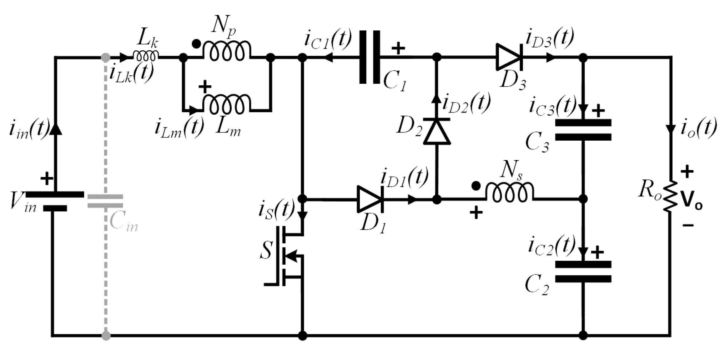
Figure 1. Proposed high-voltage-gain DC–DC converter employing coupled inductor and voltage multiplier cells.
Energies 16 03874 g001
Figure 2. Operating stages in steady state. First and fourth stages correspond to brief transition intervals that play minor roles in the energy processed by the system.
Energies 16 03874 g002
Figure 3. Main theoretical waveforms within one switching period for steady-state operation.
Energies 16 03874 g003
Figure 4. Voltage gain M as a function of the duty cycle D for different values of n and k.
Energies 16 03874 g004
Figure 5. Control strategy for the proposed converter.
Energies 16 03874 g005
Figure 6. Picture of the 400 W prototype of the proposed converter.
Energies 16 03874 g006
Figure 7. (a) Voltages and currents on the input and output; (b) Voltages on capacitors C1, C2 and C3.
Energies 16 03874 g007
Figure 8. Voltage and current on (a) switch S; (b) diode D1.
Energies 16 03874 g008
Figure 9. Voltage and current on (a) diode D2; (b) diode D3.
Energies 16 03874 g009
Figure 10. Efficiency curves: (a) as a function of the output power with Vin = 48 V and Vo = 400 V; (b) as a function of the input voltage (Vin = 38–48 V) with Po = 400 W; and (c) as a function of the input voltage (Vin = 25–40 V) with variable output power (Po = 250–400 W).
Energies 16 03874 g010aEnergies 16 03874 g010b
Figure 11. Closed-loop response for steps in the input current reference from 4.25 A to 8.75 A and from 8.75 A to 4.25 A. The output voltage is imposed by the electronic load NHR9430 operating in the constant voltage mode to emulate the behavior of a grid-tied inverter stage.
Energies 16 03874 g011
Table 1. Design specifications for a 400 W prototype.
SymbolDescriptionValue
VinInput voltage48 V
fsSwitching frequency100 kHz
PoOutput power400 W
VoOutput voltage400 V
nNumber of turns ratio1
kInductance factor95%
LkLeakage inductance2 µH
foResonant frequency1.6·fs
ILmCurrent ripple on Lm45% of Iin
VC3Voltage ripple on C31% of VC3
Table 2. Main design results.
ParameterValue
D0.644
Lm80 µH, E42/15, Np = Ns = 16
C13 µF/400 V
C23 µF/400 V
C33 µF/400 V
D1, D2 and D3MUR 840
SIRFP4668PBF
Table 3. Comparison between boost-based high-step-up DC–DC converters using a single active switch and one coupled inductor with only two windings.
ReferenceVoltage Gain (Vo/Vin)Voltage Stress on the SwitchVoltage Stress on the DiodesNumber of CapacitorsNumber of DiodesEfficiency η
VD1VD2VD3
Proposed 2 + n   1 D V i n 1 D   ( 1 + n 1 D + n ) V i n ( 1 + n 1 D + n ) V i n   V i n 1 D 3396.5% @400 W, 100 kHz, n = 1
[5] 1 + n   1 D 1 + n   1 D V i n ( 1 + n   1 D n + 1 ) V i n 1 + n   1 D V i n -2294% @300 W, 100 kHz, n = 3
[6] 1 + n   1 D V i n 1 D V i n 1 D n V i n 1 D n V i n 1 D 3396.5% @400 W, 90 kHz, n = 1.72
[13] 1 + n D   1 D V i n 1 D V i n 1 D Limited by the RCD snubber 1Voltage stress on the snubber diode 13393% @35 W, 38 kHz, n = 2
[14] 1 + n   1 D V i n 1 D V i n 1 D n V i n 1 D n V i n 1 D 33Not reported, 20 kHz, n = 1
[15] 2 1 + n   1 D + n V i n 1 D V i n 1 D n V i n 1 D n V i n 1 D 4494.3% @400 W, 50 kHz, n = 1
[16] 1 + n   1 D V i n 1 D V i n 1 D n V i n 1 D n V i n 1 D 3394% @300 W, 100 kHz, n = 6
[17] 3 2 + n   ( 1 D ) 2 V i n ( 1 D ) 2   V i n 1 D D V i n ( 1 D ) 2   V i n ( 1 D ) 2 4591.1% @500 W, 40 kHz, n = 1.86
1 Voltage stresses were not reported in the paper. 2 Voltage stress on the fourth diode is similar to D2 and D3. 3 Voltage stresses on Dr1 and Do are not included.
Disclaimer/Publisher’s Note: The statements, opinions and data contained in all publications are solely those of the individual author(s) and contributor(s) and not of MDPI and/or the editor(s). MDPI and/or the editor(s) disclaim responsibility for any injury to people or property resulting from any ideas, methods, instructions or products referred to in the content.