Article

Modeling and Control of Modular Multilevel Matrix Converter for Low-Frequency AC Transmission

Department of Electrical Engineering, Zhejiang University, Hangzhou 310027, China
*
Author to whom correspondence should be addressed.
Energies 2023, 16(8), 3474; https://doi.org/10.3390/en16083474
Submission received: 18 February 2023 / Revised: 12 April 2023 / Accepted: 13 April 2023 / Published: 15 April 2023

Abstract

:
The modular multilevel matrix converter (M3C) is the core component in low-frequency AC (LFAC) transmission, which is a competitive scheme for offshore wind power integration. In this paper, the M3C control strategy with the reduced switching frequency SM voltage balancing method is proposed. First, based on the conventional αβ0 and dq transformations, the M3C mathematical model is derived. Then, the dual-loop control structure with outer loop and inner loop controllers commonly used in voltage source converters is applied to the M3C. The inner loop controller consists of the current tracking controller in the dq reference frame and the circulating current suppressing controller in the αβ0 reference frame; the outer loop controller is proposed for the offshore wind farm LFAC integration scenario. Additionally, according to the operating characteristics of full-bridge sub-modules (FBSMs), three characteristic variables are defined and a reduced switching frequency SM voltage balancing method based on the nearest level control (NLC) is proposed. Finally, time-domain simulations in PSCAD/EMTDC demonstrate the feasibility of the proposed control strategy.

1. Introduction

With the development of offshore wind farms far from the coast, the long-distance transmission of offshore wind power has drawn extensive attention from academia and industry [1,2]. At present, the commissioned distant offshore wind farms are generally connected to onshore AC grids by high-voltage direct current (HVDC) systems [3]. However, the offshore converter platform of the HVDC scheme is costly. In addition, since the HVDC circuit breaker is extremely expensive and the weight and dimension of the HVDC circuit breaker are extremely large, the high-voltage large-capacity DC circuit breaker limits the development of the HVDC grid for offshore wind power integration. To overcome these shortcomings, the low-frequency alternating current (LFAC) transmission is proposed as an alternative, dating back to the 1950s in conception [4,5]. With the development of power electronics, the LFAC scheme is found increasingly competitive for offshore wind farm integration with technical and economic advantages: the transmission distance and capacity can be increased under lower frequency; investment costs are reduced by eliminating the offshore converter platform [6].
The onshore frequency converter is the core equipment in the LFAC system. Early research has focused on the cycloconverter, which suffers from severe harmonics and unsatisfactory fault ride-through ability [7]. The modular multilevel matrix converter (M3C), first proposed in 2001 [8], is generally regarded as the next-generation frequency converter due to its low voltage harmonic level, high scalability, and decoupled active and reactive power control [9]. Currently, the 200 kV/300 MW M3C-based Hangzhou LFAC demonstration project is under construction, and the M3C-based LFAC shows good potential in high-voltage bulk power transmission.
To apply the M3C to the LFAC system, an intuitive mathematical model and a satisfactory control strategy are crucial. The existing literature on modeling and control of the M3C is mainly based on the double αβ0 transformation, which is first proposed in [10,11] to achieve the decoupled model and control. However, the physical meaning of variables is not clear with the double αβ0 transformation. In comparison, the conventional αβ0 and dq transformations can provide more definite physical meaning, and the derivation process is more straightforward and easier to understand. For readers familiar with conventional modular multilevel converter (MMC) technology, the αβ0 and dq transformations are preferable. If the M3C can be considered as an extension of the MMC, the M3C controller design can be simplified by adopting the design method of the MMC controller.
Balancing the sub-module (SM) voltages in each arm is essential in the M3C control strategy, which is generally achieved by the voltage sorting algorithm based on the modulation method. Current studies on the M3C control are mainly based on the electric drive application [12,13], where the pulse-width modulation (PWM) is selected as the SM number is small enough. As for the LFAC transmission system, the number of series-connected SMs in each arm is sufficiently large to withstand the high voltage. In this case, the nearest level control (NLC) widely used in the MMC-based HVDC is more suitable due to lower switching losses and less calculation burden [14]. However, current studies still apply the PWM to the M3C in the LFAC system [15,16,17] and few studies mention the application of the NLC to the M3C.
In [18,19], a conventional SM voltage balancing algorithm based on the NLC is proposed, which sorts all capacitors’ voltages and triggers the SMs with the highest or lowest capacitor voltages. However, the conventional algorithm has to be executed in each control cycle. Thus, even if the total number of inserted SMs in one arm is unchanged, unnecessary switching operations are generated. To reduce the switching losses due to the unnecessary switching operations, reference [20] proposed a reduced switching frequency modulation, which considers the extra number of SMs that need to be switched on or off in the following control cycle. The conventional SM voltage balancing algorithm, a hybrid balancing algorithm, and a fundamental frequency balancing algorithm are investigated in [21]. Reference [22] proposed a reduced switching frequency algorithm with a balancing adjusting number to avoid large SM voltage fluctuation. In [23], a voltage balancing strategy juggling the low voltage deviation and the low switching frequency is proposed. However, these algorithms are suitable for the MMC with half-bridge sub-modules (HBSMs). Reference [24] introduced an optimized voltage sorting algorithm for the M3C to shorten the sorting time without affecting the switching frequency. No literature has considered the reduced switching frequency modulation in the M3C with full-bridge sub-modules (FBSMs). Considering that there are hundreds of SMs in the M3C, an SM voltage balancing method with reduced switching frequency can thus decrease the switching losses and promote the application of M3C in the LFAC system, which requires further study.
The contributions of this paper are as follows:
(1)
The mathematical model of the M3C is derived based on the extended MMC topology and the multiple αβ0 and dq transformations. The dual-loop controllers are designed according to the derived mathematical model.
(2)
A reduced switching frequency SM voltage balancing method based on the NLC is proposed. According to state sorting and incremental switching, this optimized SM voltage balancing method can avoid unnecessary switching.
The rest of this paper is organized as follows. In Section 2, the basic structure and decoupled mathematical model of the M3C are elaborated as a basis. Then, the inner loop controller is designed in Section 3. In Section 4, the reduced switching frequency SM voltage balancing method is proposed based on state sorting and incremental switching. Section 5 presents the outer loop controller. To verify the proposed control strategy, a case is presented in Section 6. Finally, conclusions are drawn in Section 7.

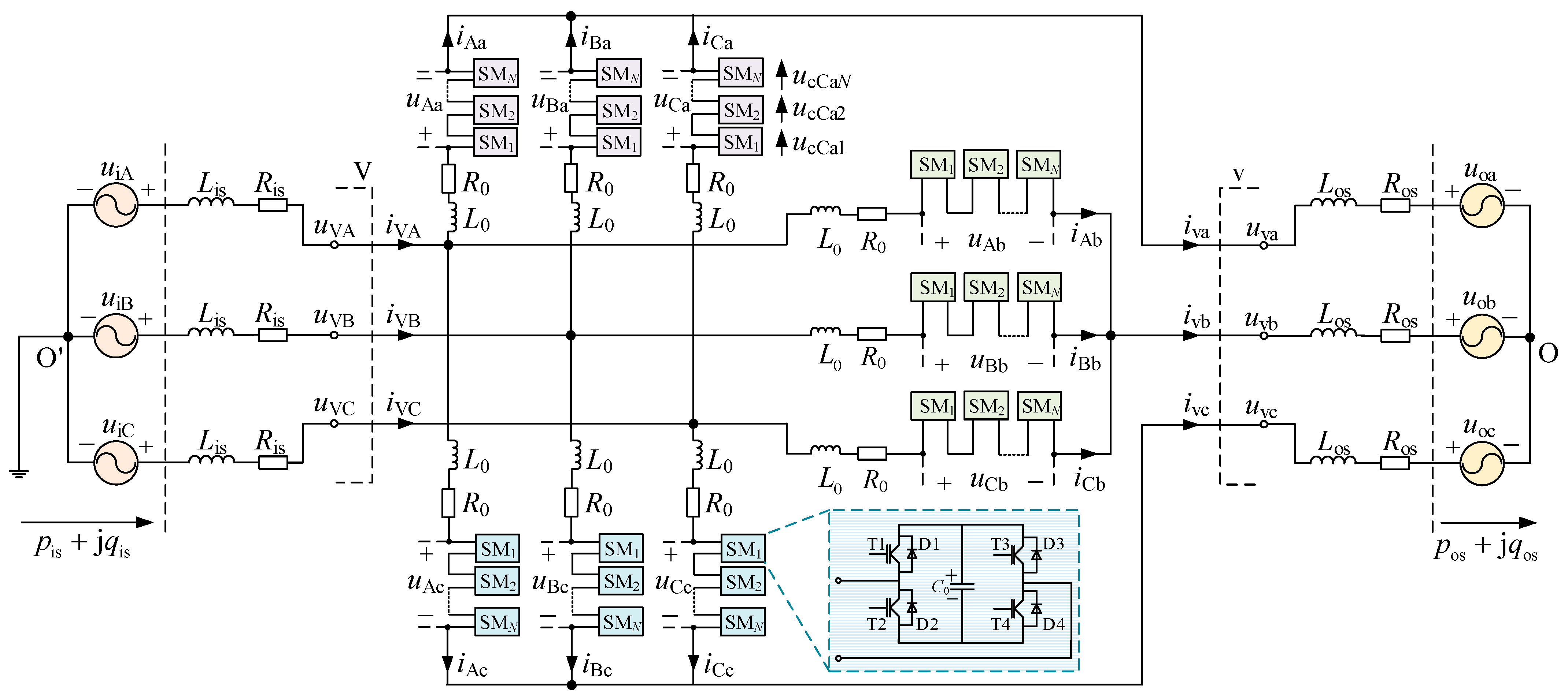
2. Basic Structure and Mathematical Model of M3C

An intuitive presentation of the main circuit structure is significant for understanding the M3C. Instead of the original presentation in [8], it is more straightforward to display the M3C main circuit structure as shown in Figure 1, which makes the M3C topology regarded as an extended MMC topology by adding three middle arms to the conventional MMC.
The physical meanings and reference directions of the basic variables in the M3C are plotted in Figure 1. j (j = A, B, C) and k (k = a, b, c) in the subscript denote phase j on the input side and phase k on the output side, respectively. uij and uok represent the system voltage on the input side and the output side. pis and qis are the instantaneous active power and reactive power of the input system. The instantaneous active power and reactive power of the output system are expressed as pos and qos. The system resistance and inductance on the input side are denoted as Ris and Lis. Ros and Los represent the system resistance and inductance on the output side. In addition, V and v are symbols of the M3C AC ports on the input side and the output side. uVj and iVj denote the M3C AC voltage and current on the input side. uvk and ivk are the M3C AC voltage and current on the output side. In addition, SMs in the M3C are FBSMs, each FBSM involves four insulated gate bipolar transistors (IGBTs) Th (h = 1, 2, 3, 4) with four anti-parallel diodes Dh and a storage capacitor C0. L0 is the arm inductance and R0 represents the equivalent arm resistance. ujk and ijk express the voltage and current of arm jk, and ucjkm is the capacitor voltage of the mth SM in arm jk. O′ and O denote the neutral point of the input side and the output side.
According to the basic structure in Figure 1, the mathematical model of the M3C is derived. First, applying the Kirchhoff’s voltage law (KVL) to Figure 1 yields:
( L 0 d d t + R 0 ) i Aa i Ab i Ac i Ba i Bb i Bc i Ca i Cb i Cc + u Aa u Ab u Ac u Ba u Bb u Bc u Ca u Cb u Cc = ( L is d d t + R is ) i VA i VA i VA i VB i VB i VB i VC i VC i VC ( L os d d t + R os ) i va i vb i vc i va i vb i vc i va i vb i vc + u iA u iA u iA u iB u iB u iB u iC u iC u iC u oa u ob u oc u oa u ob u oc u oa u ob u oc + u O O u O O u O O u O O u O O u O O u O O u O O u O O
where uO′O is the voltage difference of two neutral points.
Based on the Kirchhoff’s current law (KCL), the relationships between the arm currents and the AC currents on the input side and output side of the M3C can be expressed as:
i VA i VB i VC = i Aa i Ba i Ca + i Ab i Bb i Cb + i Ac i Bc i Cc
i va i vb i vc = i Aa i Ab i Ac + i Ba i Bb i Bc + i Ca i Cb i Cc
Define usumj (j = A, B, C) and ucomk (k = a, b, c) as the common-mode voltages on the input side and the output side:
u sumA u sumB u sumC = 1 3 u Aa + u Ab + u Ac u Ba + u Bb + u Bc u Ca + u Cb + u Cc
u coma u comb u comc = 1 3 u Aa + u Ba + u Ca u Ab + u Bb + u Cb u Ac + u Bc + u Cc
For the modeling analysis and controller design of the M3C, it is more convenient to implement in the orthogonal reference frame, where the physical quantities on each axis can be decoupled and the redundant equations can be naturally eliminated. The αβ0 reference frame is one of the most widely used orthogonal reference frames. The abc-αβ0 (ABC-αβ0) reference frame transformation matrix is defined as [25]:
T abc - α β 0 = 2 3 1 1 / 2 1 / 2 0 3 / 2 3 / 2 1 / 2 1 / 2 1 / 2
Transform the common-mode voltages usumj (j = A, B, C) and ucomk (k = a, b, c) to the αβ0 reference frame through premultiplying (4) and (5) by Tabc-αβ0:
u sum α u sum β u sum 0 = T abc - α β 0 u sumA u sumB u sumC = 1 3 u α a + u α b + u α c u β a + u β b + u β c u 0 a + u 0 b + u 0 c
u com α u com β u com 0 = 2 3 1 1 / 2 1 / 2 0 3 / 2 3 / 2 1 / 2 1 / 2 1 / 2 u coma u comb u comc
Transform the arm currents from the ABC reference frame to the αβ0 reference frame:
i α a i α b i α c i β a i β b i β c i 0 a i 0 b i 0 c = 2 3 1 1 / 2 1 / 2 0 3 / 2 3 / 2 1 / 2 1 / 2 1 / 2 i Aa i Ab i Ac i Ba i Bb i Bc i Ca i Cb i Cc
Transform the arm voltages from the ABC reference frame to the αβ0 reference frame:
u α a u α b u α c u β a u β b u β c u 0 a u 0 b u 0 c = 2 3 1 1 / 2 1 / 2 0 3 / 2 3 / 2 1 / 2 1 / 2 1 / 2 u Aa u Ab u Ac u Ba u Bb u Bc u Ca u Cb u Cc
Substituting (9) into (2) gives:
i V α i V β i V 0 = T abc - α β 0 i VA i VB i VC = i α a + i α b + i α c i β a + i β b + i β c i 0 a + i 0 b + i 0 c
Inserting (3) into (9) yields:
i 0 a i 0 b i 0 c = 1 3 i Aa + i Ba + i Ca i Ab + i Bb + i Cb i Ac + i Bc + i Cc = 1 3 i va i vb i vc
Substituting (5) into (10) gives:
u 0 a u 0 b u 0 c = 1 3 u Aa + u Ba + u Ca u Ab + u Bb + u Cb u Ac + u Bc + u Cc = 3 u coma u comb u comc
Then, transform (1) from the ABC reference frame to the αβ0 reference frame through premultiplying (1) by Tabc-αβ0:
( L 0 d d t + R 0 ) i α a i α b i α c i β a i β b i β c i 0 a i 0 b i 0 c + u α a u α b u α c u β a u β b u β c u 0 a u 0 b u 0 c = ( L is d d t + R is ) i V α i V α i V α i V β i V β i V β i V 0 i V 0 i V 0 3 ( L os d d t + R os ) 0 0 0 0 0 0 i va i vb i vc + u i α u i α u i α u i β u i β u i β u i 0 u i 0 u i 0 3 0 0 0 0 0 0 u oa u ob u oc + 3 0 0 0 0 0 0 u O O u O O u O O
Equation (14) can be split into (15) and (16), which describe the characteristics of the input side and the output side of the M3C, respectively:
( L 0 d d t + R 0 ) i α a i α b i α c i β a i β b i β c + u α a u α b u α c u β a u β b u β c = ( L is d d t + R is ) i V α i V α i V α i V β i V β i V β + u i α u i α u i α u i β u i β u i β
( L 0 d d t + R 0 ) i 0 a i 0 b i 0 c + u 0 a u 0 b u 0 c = ( L is d d t + R is ) i V 0 i V 0 i V 0 + u i 0 u i 0 u i 0 3 ( L os d d t + R os ) i va i vb i vc 3 u oa u ob u oc + 3 u O O u O O u O O
Substituting (12) and (13) into (16) gives:
[ ( L 0 + 3 L os ) d d t + ( R 0 + 3 R os ) ] i va i vb i vc + 3 u coma u comb u comc = 3 ( L is d d t + R is ) i V 0 i V 0 i V 0 + 3 u i 0 u i 0 u i 0 3 u oa u ob u oc + 3 u O O u O O u O O
Premultiplying (17) by Tabc-αβ0, the variables on the M3C output side are transformed from the abc reference frame to the αβ0 reference frame:
[ ( L 0 + 3 L os ) d d t + ( R 0 + 3 R os ) ] i v α i v β i v 0 + 3 u com α u com β u com 0 = 3 ( L is d d t + R is ) 0 0 i V 0 + 3 0 0 u i 0 3 u o α u o β u o 0 + 3 3 0 0 u O O
where iV0 = iv0 = ui0 = uo0 = 0 as the three-phase AC systems on both sides of the M3C are symmetrical. Then, (18) can be split into (19) and (20):
( L o Σ d d t + R o Σ ) i v α i v β = u com α u com β u o α u o β
u com 0 = 3 u O O
where L = Los + L0/3, R = Ros + R0/3.
Combining (7), (8), (13), and (20) gives:
u sum 0 = u com 0 = 3 u O O
Equation (15) can be split into (22)–(24):
( L 0 d d t + R 0 ) i α a i β a + u α a u β a = ( L is d d t + R is ) i V α i V β + u i α u i β
( L 0 d d t + R 0 ) i α b i β b + u α b u β b = ( L is d d t + R is ) i V α i V β + u i α u i β
( L 0 d d t + R 0 ) i α c i β c + u α c u β c = ( L is d d t + R is ) i V α i V β + u i α u i β
Adding up (22), (23), and (24) yields:
( L 0 d d t + R 0 ) i α a + i α b + i α c i β a + i β b + i β c + u α a + u α b + u α c u β a + u β b + u β c = 3 ( L is d d t + R is ) i V α i V β + 3 u i α u i β
According to (7) and (11), (25) can be rewritten as:
( L i Σ d d t + R i Σ ) i V α i V β = u sum α u sum β + u i α u i β
where L = Lis + L0/3, R = Ris + R0/3.
Define ilcir1 and ilcir2 (l = α, β) as circulating currents in the αβ0 reference frame as in (27); define ulcir1 and ulcir2 (l = α, β) as circulating voltages in the αβ0 reference frame as in (28):
i α b i α a i β b i β a = i α cir 1 i β cir 1 , i α c i α a i β c i β a = i α cir 2 i β cir 2
u α b u α a u β b u β a = u α cir 1 u β cir 1 , u α c u α a u β c u β a = u α cir 2 u β cir 2
Subtracting (22) from (23) and (24), respectively, the relationship between the circulating currents and the circulating voltages can be described as:
( L 0 d d t + R 0 ) i α cir 1 i β cir 1 + u α cir 1 u β cir 1 = 0
( L 0 d d t + R 0 ) i α cir 2 i β cir 2 + u α cir 2 u β cir 2 = 0
It is noticed that the circulating currents are only determined by the arm reactance and the arm voltage inside the M3C and have no direct relationship with the input side and the output side of the M3C.
Hence, (19), (21), (26), (29), and (30) constitute the 9th order mathematical model of the M3C in the αβ0 reference frame.
To simplify the controller design, (19) and (26) corresponding to the external quantities of the M3C are transformed to the dq reference frame. The αβ0-dq reference frame transformation matrices on the input side and the output side of the M3C are defined as [25]:
T α β 0 - dq ω i = cos ω i t sin ω i t sin ω i t cos ω i t
T α β 0 - dq ω o = cos ω o t sin ω o t sin ω o t cos ω o t
where ωit is the voltage phase angle of phase-A of the input system and ωot is the voltage phase angle of phase-a of the output system, both of which are acquired by the phase-locked loop (PLL).
Premultiplying (26) and (19) by (31) and (32), respectively, the input and output side characteristics of the M3C in the dq reference frame can be expressed as:
L i Σ [ d d t 0 ω i ω i 0 ] i Vd i Vq + R i Σ i Vd i Vq + u sumd u sumq = u id u iq
L o Σ [ d d t 0 ω o ω o 0 ] i vd i vq + R o Σ i vd i vq + u comd u comq = u od u oq
Until now, the mathematical model of the M3C has been derived based on the extended MMC topology in Figure 1 and the multiple αβ0 and dq transformations, as shown in (21), (29), (30), (33), and (34). The major benefits of the multiple αβ0 and dq transformations are in the following three aspects:
(1) By applying the multiple αβ0 and dq transformations, the derivation process can be more straight forward and easier to understand.
(2) Through the multiple αβ0 and dq transformations, the mathematical models of the input side and the output side of the M3C are basically consistent with the AC side mathematical model of the MMC. Thus, one M3C is equivalent to two decoupled MMCs on the input side and the output side. In other words, the M3C can be considered as an extension of the conventional MMC, which is beneficial for analyzing the M3C operating characteristics.
(3) The design of the M3C controller can be transformed into the design of controllers for two MMCs. In this way, the design method of the MMC controller can be adapted to the M3C controller design directly, which is beneficial for simplifying the M3C controller design.

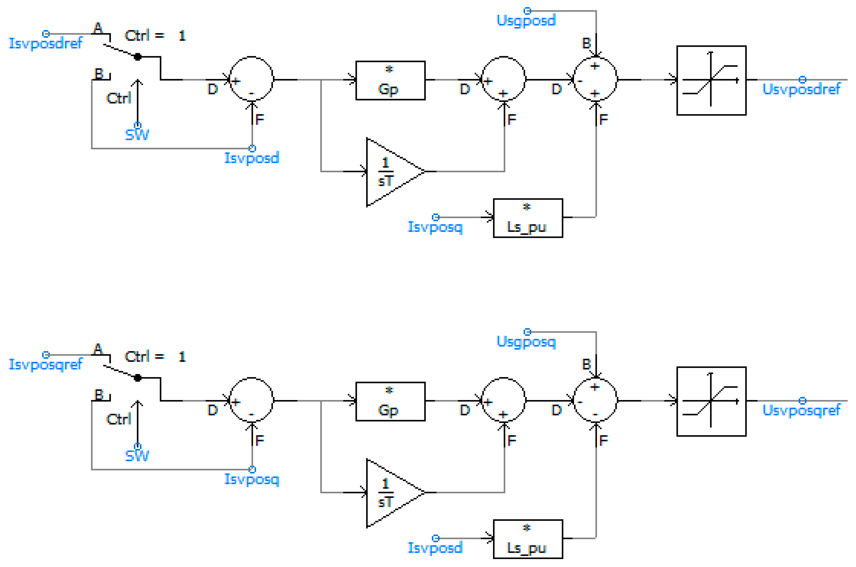
3. Inner Loop Controller

Based on the previously derived mathematical model, the inner loop controller is divided into two parts to control the external characteristics and internal characteristics of the M3C, respectively. The current tracking controller of the external characteristics on the input and output sides described by (10) and (11) is designed in the dq reference frame. The circulating current suppressing controller of the internal characteristics expressed by (5) and (6) is designed in the αβ0 reference frame. The outputs of the inner loop controller are integrated to obtain the voltage references of the 9 arms of the M3C.

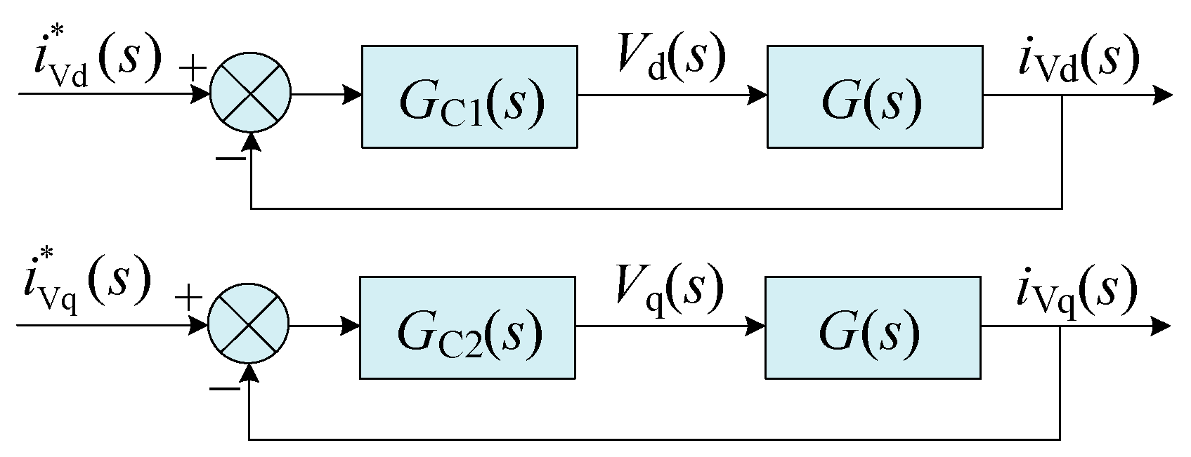
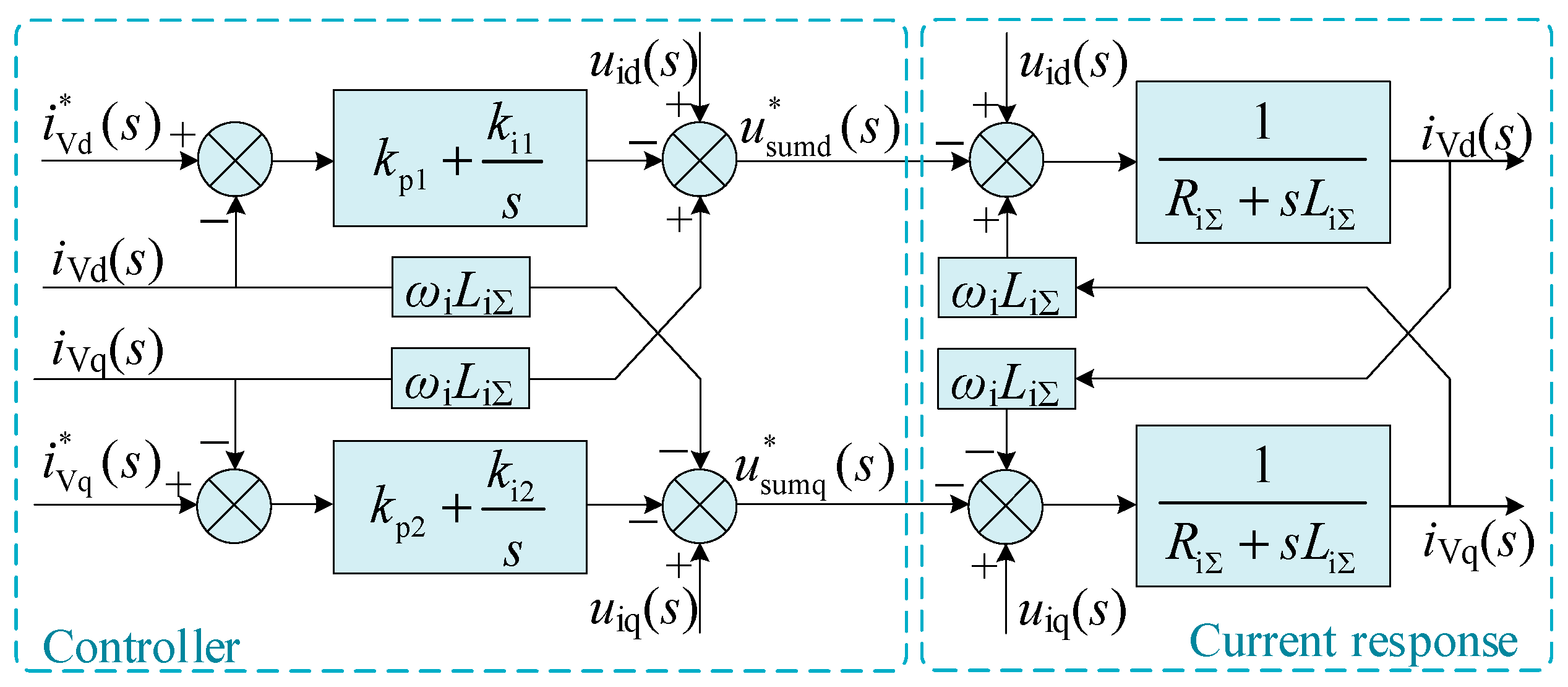
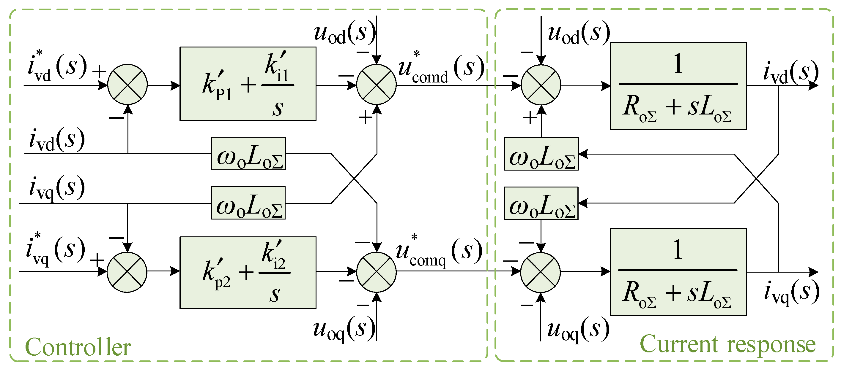
3.1. Current Tracking Controller

By Laplace transform of (10), the dynamic characteristics of the input side in the s domain are represented as:
( R i Σ + L i Σ s ) i Vd ( s ) = u id ( s ) u sumd ( s ) + ω i L i Σ i Vq ( s ) ( R i Σ + L i Σ s ) i Vq ( s ) = u iq ( s ) u sumq ( s ) ω i L i Σ i Vd ( s )
From (35), it is noticed that the currents on the input side (output variables) are determined by the system voltages (disturbance variables) and the common-mode voltages (control variables) on the input side. The current tracking controller on the input side is to obtain control variable references usumd* and usumq* by making output variables track their references iVd* and iVq*.
To simplify the controller design, substituting variables in (35) with new control variables denoted by Vd and Vq yields:
V d ( s ) = u id ( s ) u sumd ( s ) + ω i L i Σ i Vq ( s ) V q ( s ) = u iq ( s ) u sumq ( s ) ω i L i Σ i Vd ( s )
According to (35) and (36), the transfer function between output variables and new control variables can be expressed as:
i Vd ( s ) V d ( s ) = 1 R i Σ + L i Σ s = G ( s ) i Vq ( s ) V q ( s ) = 1 R i Σ + L i Σ s = G ( s )
Based on the classical negative feedback control theory, the control system with the simplest negative feedback shown in Figure 2 is adopted to make the output variables track their references.
In Figure 2, GC1(s) and GC2(s) are transfer functions of the d-axis controller and the q-axis controller, respectively:
G C 1 ( s ) = k p 1 + k i 1 s G C 2 ( s ) = k p 2 + k i 2 s
where kpg and kig (g = 1, 2) are parameters of the current tracking proportional–integral (PI) controller on the input side.
According to (36), (37), (38), and Figure 2, the block diagram of the current controller and the system dynamic of the input side is illustrated in Figure 3.
Similar to the design of the current tracking controller on the input side, applying the Laplace transform on (34) yields:
R o Σ + L o Σ s i vd ( s ) = u od ( s ) u comd ( s ) + ω o L o Σ i vq ( s ) R o Σ + L o Σ s i vq ( s ) = u oq ( s ) u comq ( s ) ω o L o Σ i vd ( s )
It is obvious that the current on the output side (the output variables) depends on the system voltage and the common-mode voltage (the input variables) of the output side. The current tracking controller on the output side is to obtain the input variable references ucomd* and ucomq* by making output variables track their reference values ivd* and ivq*.
The design steps of the current tracking controller on the output side are similar to those on the input side. The controller block diagram is illustrated in Figure 4, where kpg’ and kig’ (g = 1, 2) are the parameters of the current tracking PI controller on the output side.

3.2. Circulating Current Suppressing Controller

Circulating currents only flow among the arms and produce no direct effects on either the input side or the output side of the M3C. The circulating currents will increase the power losses in the M3C and usually need to be suppressed. The circulating currents contain harmonic components of various frequencies, and it is unnecessary to design the controllers for each harmonic in the circulating currents. Therefore, the simple proportional controller as in (40) and (41) can be adopted for suppressing the circulating currents in the αβ0 reference frame. According to the relationship between the circulating voltages and the circulating currents in (29) and (30), the negative feedback theory can be adopted. The circulating voltage references ulcir1* and ulcir2* (l = α, β) can be obtained by making circulating currents track their references ilcir1* and ilcir2*:
u α cir 1 * u β cir 1 * = k cir 1 i α cir 1 * i α cir 1 i β cir 1 * i β cir 1
u α cir 2 * u β cir 2 * = k cir 2 i α cir 2 * i α cir 2 i β cir 2 * i β cir 2
where kcir1 and kcir2 are proportional coefficients of the circulating current suppressing controller, and circulating current references ilcir1* and ilcir2* are usually set as 0.

3.3. Calculation of Arm Voltage References

The key of the M3C controller design is to determine the voltage values that the 9 arms need to generate at any time, namely, the arm voltage references. The current tracking controller on the input side designed above generates references of the common-mode voltage on the input side, denoted as usumd* and usumq*. Analogously, the references of the common-mode voltage on the output side ucomd* and ucomq* are acquired by the current tracking controller on the output side. The voltage references in the dq reference frame should be converted back to the αβ0 reference frame to obtain usumα*, usumβ*, ucomα*, and ucomβ*. Moreover, uO′O* is set as 0. In addition, the circulating voltage references are attained in (40) and (41). Thus, the arm voltage references can be obtained as:
U arm * = u Aa * u Ab * u Ac * u Ba * u Bb * u Bc * u Ca * u Cb * u Cc * = 2 3 1 1 / 2 1 / 2 0 3 / 2 3 / 2 1 / 2 1 / 2 1 / 2 T U α β * U 0 *
where Uαβ* and U0* are calculated as:
U α β * = u sum α * u α cir 1 * u α cir 2 * u sum β * u β cir 1 * u β cir 2 * T 1 / 3 1 1 1 / 3 1 0 1 / 3 0 1 1
U 0 * = 2 u com α * u com β * u com 0 * T 1 1 / 2 1 / 2 0 3 / 2 3 / 2 1 / 2 1 / 2 1 / 2

4. SM Voltage Balancing Method

After obtaining the arm voltage references, the resulting issue is to determine how to switch the SMs to make each arm voltage track its reference and maintain voltage balance among all SMs in one arm. Meanwhile, unnecessary switching operations should be avoided to minimize the switching frequency. To achieve these objectives, a reduced switching frequency SM voltage balancing method is proposed in this section.

4.1. Operating Characteristics of FBSM

The SMs constituting the M3C are FBSMs, each of which involves four IGBTs Th (h = 1, 2, 3, 4) with four anti-parallel diodes Dh and an SM capacitor C0. The output voltage of the SM is represented as usm, and Uc denotes the rated SM capacitor voltage. The positive direction of the capacitor current is consistent with that of the arm current indicated in Figure 1, which is defined as the capacitor charging direction. The operating states of the FBSM are summarized in Table 1.
According to Table 1, it can be concluded that the operating states of the FBSM are only related to the conduction state of IGBTs. The first three normal operating states can be classified based on the polarity of the output voltage of the FBSM and the last state is abnormal, which is used during system startup or fault clearing. Moreover, the SM capacitor will not be charged in the bypassed state.

4.2. Switching Strategy of SM

Define the three characteristic variables Sstate, Darm, and Cchange as:
S state = sign ( u j k * ) = 1   if   u j k * 0   1   if   u j k * < 0
D arm = sign ( i arm ) = 1   if   i arm 0   1   if   i arm < 0
C charge = S state D arm = 1 1
where ujk* is the voltage reference of arm jk (j = A, B, C and k = a, b, c), and iarm is the arm current. Sstate represents the direction of the arm voltage, Darm denotes the direction of the arm current, and Cchange expresses the charging/discharging state of the SM capacitor. According to Table 1, the charging/discharging state of the capacitor is related to both the direction of the arm voltage and the direction of the arm current. If Cchange = 1, it means that the capacitor is in the charging state; if Cchange = −1, it means that the capacitor is in the discharging state.
The voltages of each arm are synthesized by the SM capacitor voltages. The number of the inserted SMs in arm jk is calculated as:
n j k = round ( u j k * U c ) 0
where round() is the function to calculate the nearest integer; Uc denotes the rated SM voltage capacitor.
The variation of njk between two adjacent control moments is defined as:
Δ n j k = n j k n j k , old   if   S state = S state , old n j k   if   S state S state , old
where the subscript ‘old’ expresses the value at the previous control moment.
The conventional SM voltage balancing algorithm based on sorting all capacitors’ voltages proposed in [18] is as follows:
  • When the arm current charges the capacitors (Cchange = 1), njk SMs with the lowest capacitor voltages are inserted positively or negatively according to Sstate and the other SMs are bypassed.
  • When the arm current discharges the capacitors (Cchange = −1), njk SMs with the highest capacitor voltages are inserted positively or negatively according to Sstate and the other SMs are bypassed.
The conventional algorithm will result in a high switching frequency since the switchings of SMs are based on the SM capacitor voltages only at the present moment regardless of the previous state of SMs.
To decrease switching frequency by avoiding unnecessary switchings, a reduced switching frequency SM voltage balancing method is proposed as shown in Figure 5. This optimized balancing method considers the previous state of SMs and performs incremental switching as follows:
  • If Δnjk = 0, SMs in arm jk have no switching operation at the current control moment and directly wait for the next control moment.
  • If Δnjk > 0, the number of the inserted SMs should be increased. Then, if Cchange = 1, Δnjk SMs with the lowest voltage are inserted; if Cchange = −1, Δnjk SMs with the highest voltage are inserted. Sstate determines whether the insertion is positive or negative.
  • If Δnjk < 0, the number of the inserted SMs should be decreased. Then, if Cchange = 1, Δnjk SMs with the highest voltage are bypassed, and if Cchange = −1, Δnjk SMs with the lowest voltage are bypassed.
Figure 5. Reduced switching frequency SM voltage balancing method based on state sorting and incremental switching.
Energies 16 03474 g005

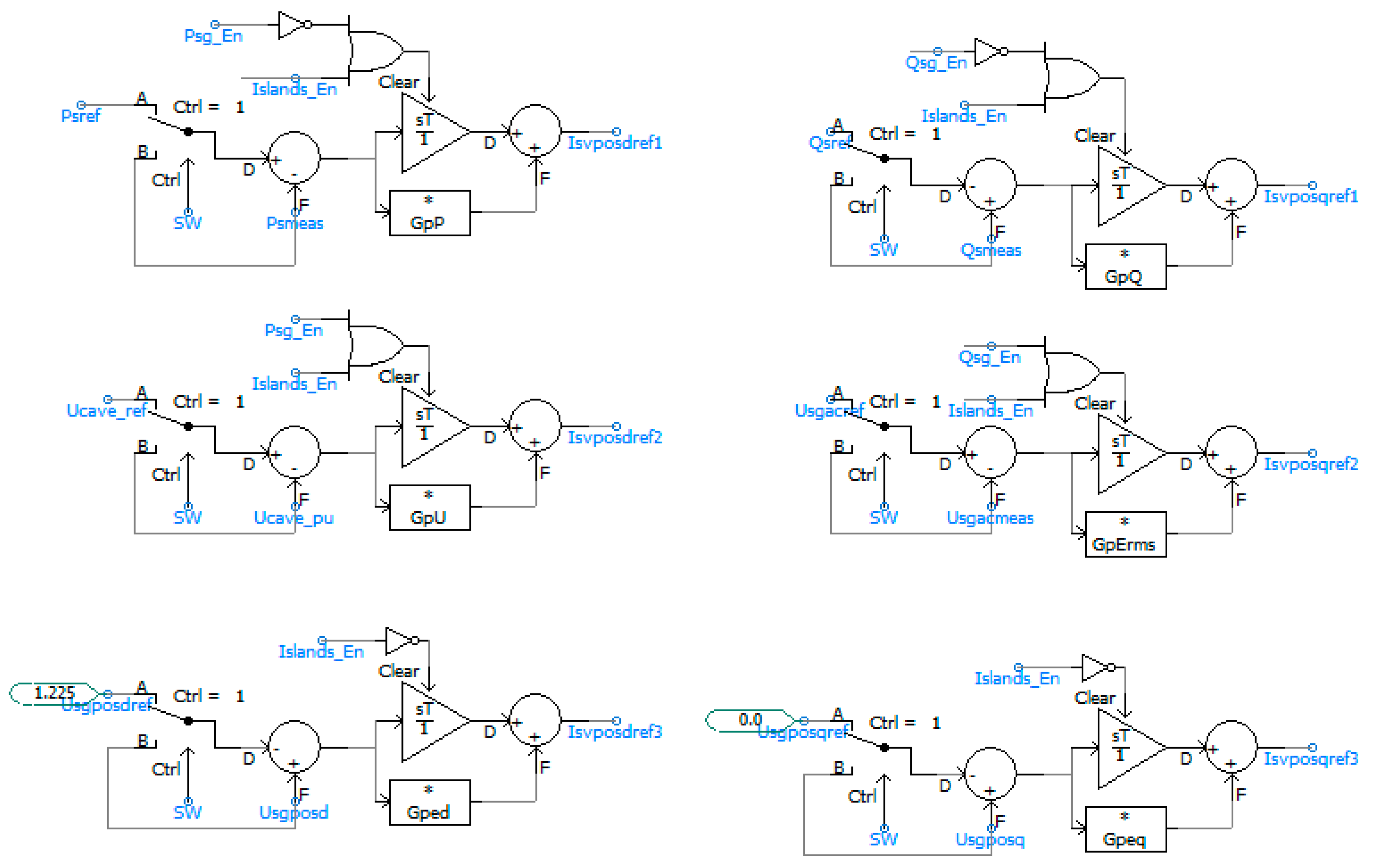
5. Outer Loop Controller

The outer loop controller is required for both the input side and the output side of the M3C. For the scenario of M3C-based offshore wind power LFAC integration, the input side of the M3C is connected to the offshore AC system with grid-following wind turbines, and the input side should operate in the V/f mode to provide stable AC voltage support; the output side of the M3C is connected to the onshore AC grid, and the control target is to maintain the SM capacitor voltage. The outer loop controller is designed according to the reference direction as shown in Figure 1.

5.1. Outer Loop Controller on Input Side

The input side of the M3C should operate in the V/f mode to provide stable AC voltage support for the offshore wind farm. There are two control objectives: one is to control the frequency of the offshore system to the rated frequency and the other is to control the voltage amplitude of the input side AC bus constant.
The outer loop control strategy on the input side of the M3C has two significant characteristics:
(1)
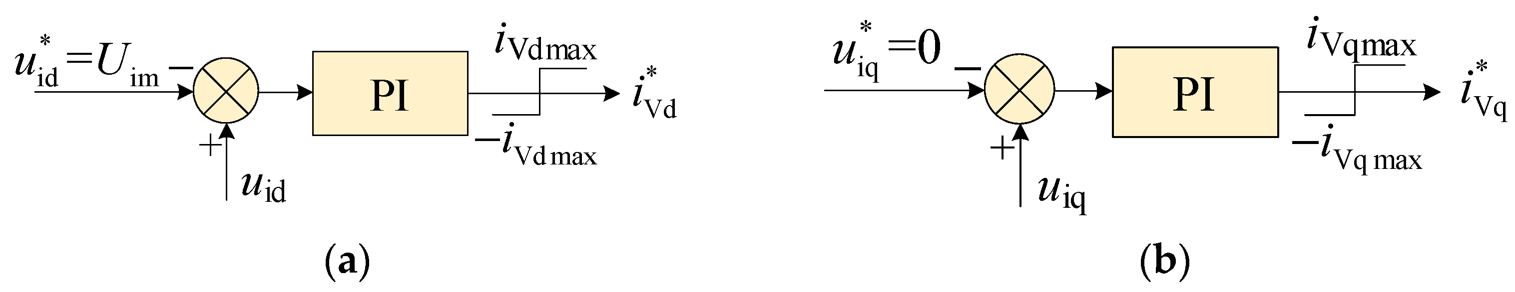
PLL is no longer needed because the frequency of the offshore system is given, i.e., the electrical angle is completely determined and the rotating speed of the dq reference frame is fixed.
(2)
Define the space vector of the AC bus voltage on the input side as uis. The outer loop controller on the input side is used for keeping the amplitude of uis unchanged and keeping uis aligned with the d-axis. In other words, the constant amplitude of uis means that the voltage amplitude of the input side AC bus is constant; the alignment of uis with the d-axis means that the voltage frequency of the input side AC bus equals the rated frequency.
To achieve the above two points, the outer loop controller on the input side makes uid = Uim by controlling the d-axis current reference iVd*, and uiq = 0 by controlling the q-axis current references iVq*. iVd* and iVq* are the current references for the current tracking controller on the input side of the M3C. Moreover, limiters are added to ensure that the current references are within the upper limits. The upper limits vary with operating conditions and can be simplified as:
i Vdmax = I Vmmax 2 i Vq 2 ( t T ctrl ) i Vqmax = I Vmmax 2 i Vd 2 ( t T ctrl )
where IVmmax denotes the maximum current on the input side, which can be derived from the rated capacity and the rated AC voltage; iVd(tTctrl) (or iVq(tTctrl)) is the d-axis (or q-axis) current on the input side measured in the previous control period.
After considering the above factors, the structure of the outer loop controller on the input side of the M3C is shown in Figure 6.

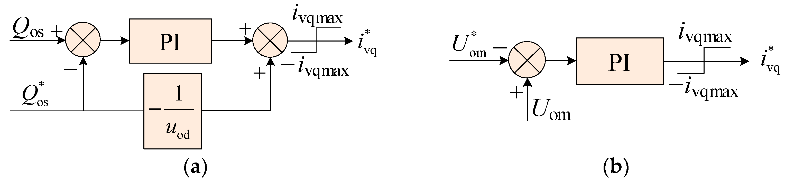
5.2. Outer Loop Controller on the Output Side

The instantaneous active power pos and the instantaneous reactive power qos on the M3C output side can be expressed as:
p os q os = u od u oq u oq u od i vd i vq
In the steady state, the q-axis component of the output side system voltage uoq is 0, and the d-axis component of the output side system voltage uod is equal to the system voltage amplitude Uom. Thus, (51) can be rewritten as:
p os = u od i vd = U om i vd
q os = u od i vq = U om i vq
The control objectives of the outer loop controller on the output side are divided into two categories, including the active power control objective and the reactive power control objective:
(1)
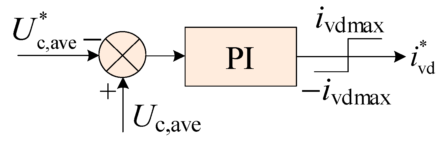
The reference of the active power control is the average capacitor voltage of all SMs Uc,ave*; from the perspective of energy balance, this side behaves as a power balance station.
(2)
Either the reactive power Qos* or the AC voltage amplitude Uom* on the output side is the reference of the reactive power control.
The outputs of the outer loop controller on the output side are the d- and q-axis current references ivd* and ivq* for the current tracking controller on the output side. When the vector current control is adopted, the active power control loop and the reactive power control loop can be decoupled.

5.2.1. Active Power Control Loop

The active power control loop has to maintain the SM capacitor voltage as shown in Figure 7. Moreover, considering that the M3C cannot be overloaded, the output ivd* of the active power control loop shall be limited. The upper limit ivdmax can be calculated as:
i vdmax = I vmmax 2 i vq 2 ( t T ctrl )
where Ivmmax denotes the maximum current on the output side; ivq(tTctrl) is the q-axis current on the output side measured in the previous control period.

5.2.2. Reactive Power Control Loop

In accordance with (53), ivq* can be directly calculated when Qos* is given; yet to eliminate the steady-state error, the negative feedback of the reactive power by the PI controller is required. Therefore, the reactive power control loop with given Qos* is illustrated in Figure 8a. Figure 8b represents the reactive power control loop with prescribed Uom*. In addition, the output ivq* of the reactive power control loop should be limited to avoid the overload of the M3C. Analogously, the upper limit ivqmax is given by:
i vqmax = I vmmax 2 i vd 2 ( t T ctrl )
where ivd(tTctrl) is the d-axis current on the output side measured in the previous control period.

6. Case Study

To verify the effectiveness of the proposed control strategy of the M3C, the electromagnetic transient simulation model of the M3C-based offshore wind power LFAC transmission system is established in PSCAD/EMTDC. The structure of the simulation model is shown in Figure 9 and the main circuit parameters are listed in Table 2. The detailed PSCAD/EMTDC models of the main circuit, the outer loop controller, and the inner loop controller of the M3C are shown in Figure A1, Figure A2 and Figure A3 in Appendix A.
In the test system, the input side of the M3C is connected to the offshore AC system. Thus, the input side of the M3C is operating in the V/f mode to establish the offshore AC voltage so that the wind turbine can work in the grid-following mode. The output side of the M3C is connected to the onshore AC grid. The goal of maintaining the SM capacitor voltage is accomplished by the output side of the M3C. Moreover, the output side of the M3C controls the reactive power output to the onshore grid as 0.

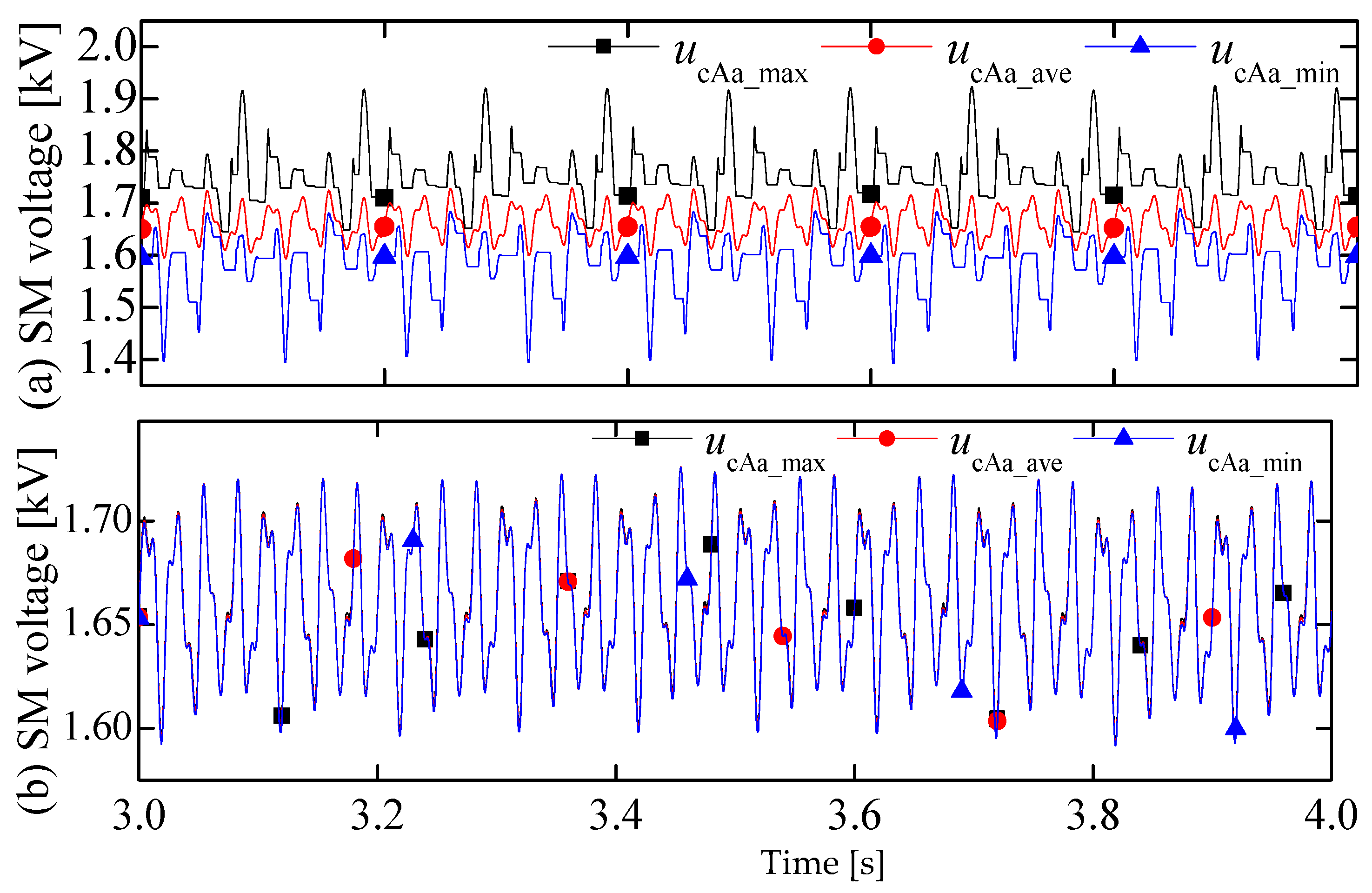
6.1. Characteristics of Reduced Switching Frequency SM Voltage Balancing Method

To verify the reduced switching frequency SM voltage balancing method, the voltage of the SMs in arm Aa is compared under the optimized balancing method in Figure 10a and the conventional balancing method in Figure 10b. The instantaneous maximum value, the instantaneous average value, and the instantaneous minimum value of all SM capacitor voltages in arm Aa are denoted as ucAa_max, ucAa_ave, and ucAa_min, respectively. Figure 11a,b compare the gate signals of one SM in arm Aa under different balancing methods. The average switching frequency of a single SM can be calculated as:
f sw _ ave = N switch N SM
where Nswitch denotes the sum of switching times per second of all SMs in one arm. Both switching-on and switching-off are counted in Nswitch. NSM is the number of SMs per arm.
As shown in Figure 10a,b, the average SM voltages of both methods are stable. With the conventional method, the voltage of all SMs in one arm is highly consistent as in Figure 10b, but the average switching frequency fsw_ave is very high (4223 Hz in Figure 11b). In comparison, the average switching frequency fsw_ave with the proposed reduced switching frequency method is much lower (93 Hz in Figure 11a) and the SM voltages are also well balanced.
To reduce the switching frequency caused by the SM voltage balancing method, the SM voltage ripple will inevitably increase. It is true that the higher the switching frequency is, the more consistent the SM capacitor voltages are. However, the high switching frequency leads to high switching losses, which defects the economic benefit of the M3C project. In fact, excessive consistency of the SM voltages is not necessary, as long as the following two requirements of the SM capacitor voltage can be satisfied:
(1)
The SM capacitor voltage should keep balanced, i.e., the average voltage of all SM capacitors does not deviate too much from the rated value.
(2)
The maximum SM capacitor voltage should be within the upper limit voltage of the SM capacitor (usually 1.2 times the rated SM voltage).
It is observed from simulation results that these two requirements can be met with the proposed reduced switching frequency method, which means that the negative impact on the SM capacitor voltage ripple is acceptable.
In practical engineering, the aforementioned two requirements can be achieved by the selection of the SM capacitor and the rated SM voltage. Thus, higher fluctuation in the SM capacitor voltage within the allowable voltage range is not a severe problem.
The above comparisons are summarized in Table 3.

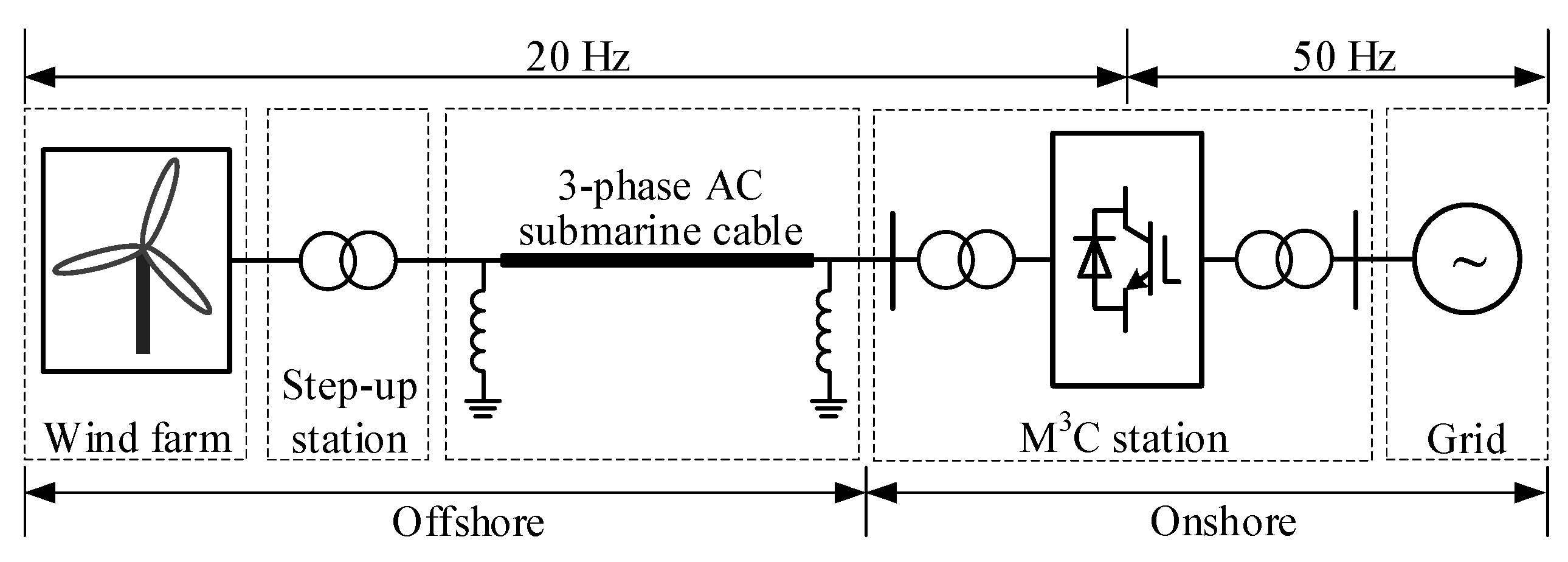
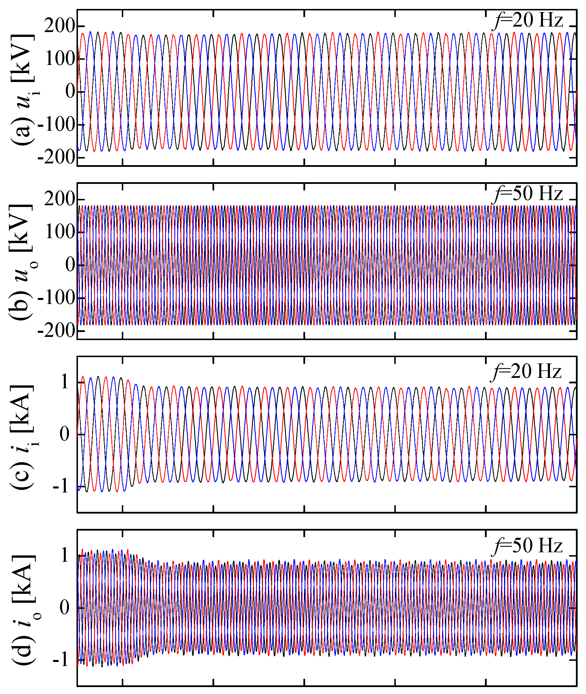
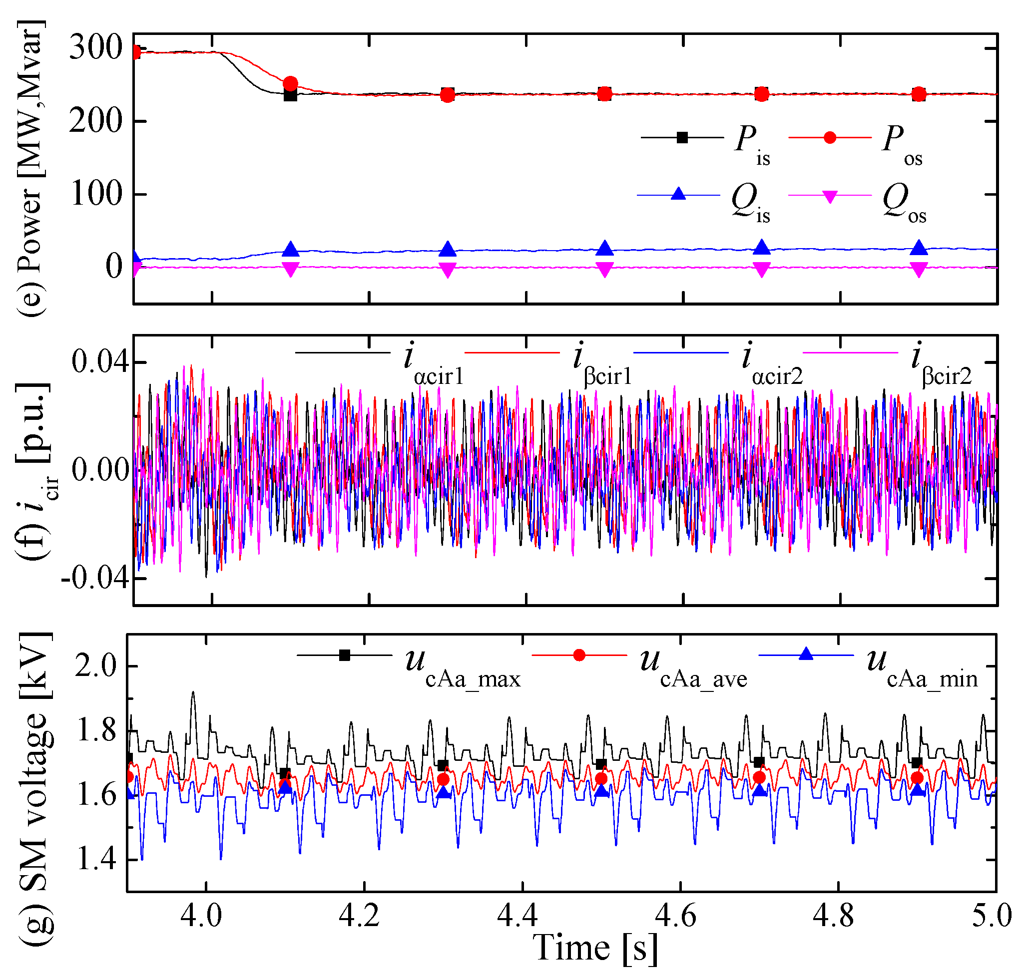
6.2. Wind Speed Fluctuation

After the simulation model enters the steady-state operation, the active power generated by the wind farm drops from 1.0 p.u. to 0.8 p.u. at t = 4.0 s due to the wind speed fluctuation. The response characteristics of the M3C are shown in Figure 12.
It can be seen from Figure 12 that after the input power from the wind farm drops, the whole system can smoothly transition to a stable operating state, and the active power at the low-frequency side and the power frequency side of M3C will decrease steadily. The SM capacitor voltage can keep balanced, and the maximum SM capacitor voltage decreases a little when the transmitted active power drops. The output side of the M3C controls the output reactive power at its reference, which is set as 0. Thus, the reactive power output to the onshore grid Qos is 0. Because the input side of the M3C operates in the V/f mode to establish the offshore AC voltage, the input side of the M3C functions as a power balancing bus for the low-frequency AC network, and the reactive power absorbed from the input side Qis is about 11 Mvar in the steady state.

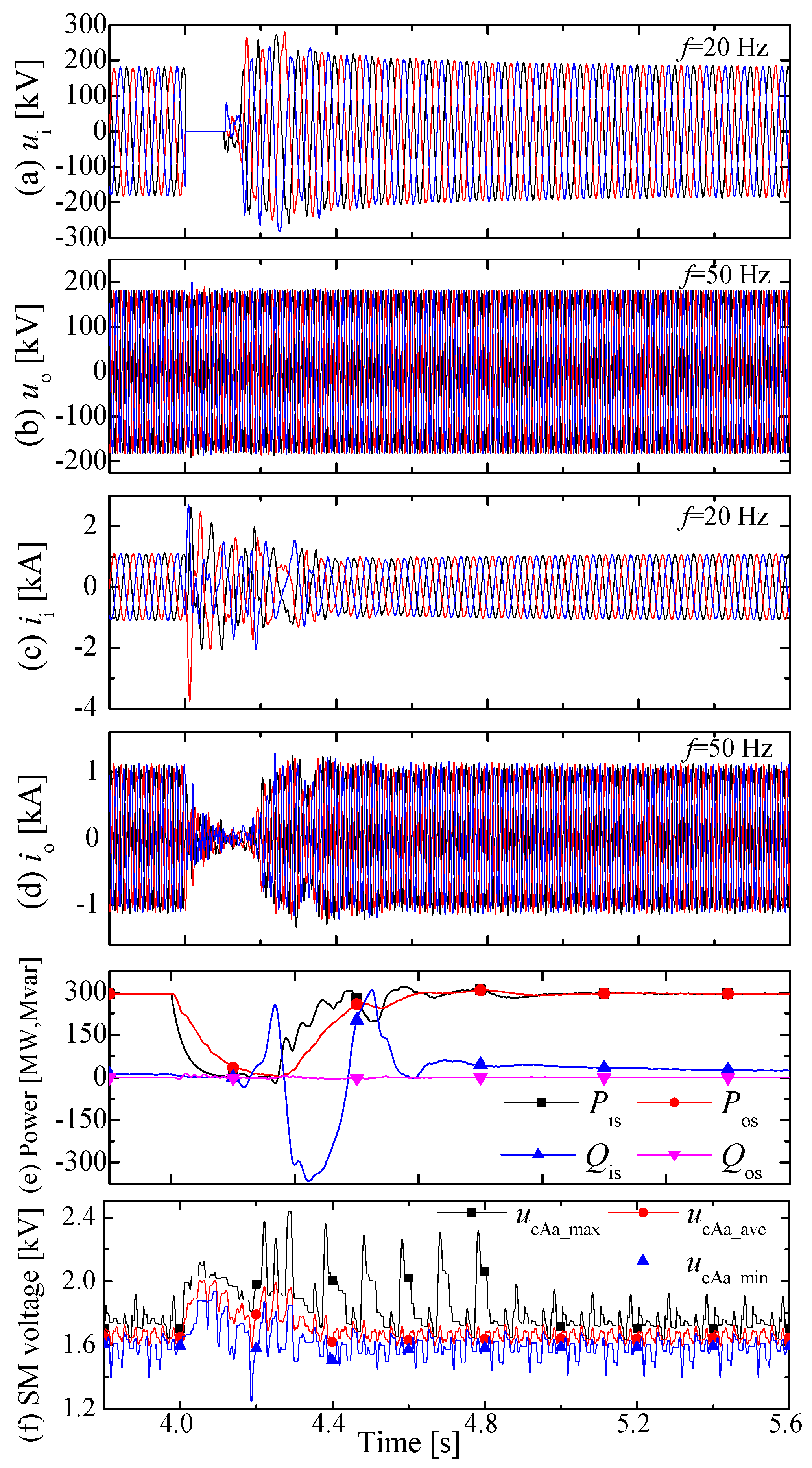
6.3. Offshore Side Fault

The system entered the steady state before the fault. Assuming that a solid three-phase-to-ground fault at the M3C offshore side AC bus occurs at 4.0 s and lasts 100 ms, the system responses are plotted in Figure 13.
When the fault occurs, the AC bus voltage on the M3C offshore side drops to 0 instantaneously, and the active power transmission from the offshore wind farm is blocked. Due to the SM capacitor voltage control, the active power transmitted to the onshore grid also drops to 0 during the fault to maintain the SM capacitor voltage. When the fault is cleared, the AC voltage recovers and the active power transmission resumes. The SM capacitor voltages do not deviate too much from the rated value during the fault and recover quickly when the fault is cleared.

7. Conclusions

A control strategy with a novel SM voltage balancing method of the M3C is proposed in the paper. The conclusions are summarized as follows:
(1)
The ninth order mathematical model of the M3C is derived based on the extended MMC topology and the multiple αβ0 and dq transformations, making the M3C equivalent to two decoupled MMCs on the input side and the output side. The detailed equations of the current tracking controller are deduced in the dq reference frame and the circulating current suppressing controller is designed in the αβ0 reference frame. The outer loop controller is proposed for the scenario of offshore wind power LFAC integration based on M3C.
(2)
A reduced switching frequency SM voltage balancing method of the M3C is proposed based on three characteristic variables and the NLC, which not only meet the requirements of SM capacitor voltage balance but also immensely reduce switching frequency. Simulation results in PSCAD/EMTDC verify the availability of the proposed control strategy.

Author Contributions

Conceptualization, Z.X.; methodology, Z.X.; software, Y.J.; validation, Z.Z. and Z.X.; formal analysis, Z.Z., Y.J. and Z.X.; investigation, Z.Z. and Y.J.; resources, Z.Z. and Z.X.; writing—original draft preparation, Y.J.; writing—review and editing, Z.Z.; visualization, Y.J. All authors have read and agreed to the published version of the manuscript.

Funding

This research received no external funding.

Data Availability Statement

Not applicable.

Conflicts of Interest

The authors declare no conflict of interest.

Appendix A

Figure A1. Simulation model of M3C main circuit.
Energies 16 03474 g0a1
Figure A2. Simulation model of M3C outer loop controller.
Energies 16 03474 g0a2
Figure A3. Simulation model of M3C inner loop controller.
Energies 16 03474 g0a3

References

  1. Apostolaki-Iosifidou, E.; Mccormack, R.; Kempton, W.; Mccoy, P.; Ozkan, D. Transmission design and analysis for large-scale offshore wind energy development. IEEE Power Energy Technol. Syst. J. 2019, 6, 22–31. [Google Scholar] [CrossRef]
  2. Erlich, I.; Shewarega, F.; Feltes, C.; Koch, F.W.; Fortmann, J. Offshore wind power generation technologies. Proc. IEEE 2013, 101, 891–905. [Google Scholar] [CrossRef]
  3. Bresesti, P.; Kling, W.L.; Hendriks, R.L.; Vailati, R. HVDC connection of offshore wind farms to the transmission system. IEEE Trans. Energy Convers. 2007, 22, 37–43. [Google Scholar] [CrossRef]
  4. Rusk, A.; Rathsman, B.G.; Glimstedt, U. The HVDC Power Transmission from Swedish Mainland to the Swedish Island of Gotland; CIGRE Report No. 406; CIGRE: Paris, France, 1950. [Google Scholar]
  5. Adamson, C.; Hingorani, N.G. High Voltage Direct Current Power Transmission; Garrway Limited: London, UK, 1960. [Google Scholar]
  6. Chen, H.; Johnson, M.H.; Aliprantis, D.C. Low-frequency AC transmission for offshore wind power. IEEE Trans. Power Deliv. 2013, 28, 2236–2244. [Google Scholar] [CrossRef]
  7. Qin, N.; You, S.; Xu, Z.; Akhmatov, V. Offshore wind farm connection with low frequency AC transmission technology. In Proceedings of the IEEE Power and Energy Society General Meeting, Calgary, AB, Canada, 26–30 July 2009; pp. 1–8. [Google Scholar]
  8. Erickson, R.W.; Al-Naseem, O.A. A new family of matrix converters. In Proceedings of the 27th Annual Conference of the IEEE Industrial Electronics Society, Denver, CO, USA, 29 November–2 December 2001; pp. 1515–1520. [Google Scholar]
  9. Luo, J.; Zhang, X.; Xue, Y.; Gu, K.; Wu, F. Harmonic analysis of modular multilevel matrix converter for fractional frequency transmission system. IEEE Trans. Power Deliv. 2020, 35, 1209–1219. [Google Scholar] [CrossRef]
  10. Kawamura, W.; Akagi, H. Control of the modular multilevel cascade converter based on triple-star bridge-cells (MMCC-TSBC) for motor drives. In Proceedings of the IEEE Energy Conversion Congress and Exposition (ECCE), Raleigh, NC, USA, 15–20 September 2012; pp. 3506–3513. [Google Scholar]
  11. Kawamura, W.; Hagiwara, M.; Akagi, H. Control and experiment of a modular multilevel cascade converter based on triple-star bridge cells. IEEE Trans. Ind. Appl. 2014, 50, 3536–3548. [Google Scholar] [CrossRef]
  12. Nakamori, T.; Sayed, M.; Hayashi, Y.; Takeshita, T.; Hamada, S.; Hirao, K. Independent control of input current, output voltage, and capacitor voltage balancing for a modular matrix converter. IEEE Trans. Ind. Appl. 2015, 51, 4623–4633. [Google Scholar] [CrossRef]
  13. Diaz, M.; Cardenas, R.; Espinoza, M.; Hackl, C.; Rojas, F.; Clare, J.; Wheeler, P. Vector control of a modular multilevel matrix converter operating over the full output-frequency range. IEEE Trans. Ind. Electron. 2019, 66, 5102–5114. [Google Scholar] [CrossRef]
  14. Perez, M.; Rodriguez, J.; Pontt, J.; Kouro, S. Power distribution in hybrid multi-cell converter with nearest level modulation. In Proceedings of the IEEE International Symposium on Industrial Electronics, Vigo, Spain, 4–7 June 2007; pp. 736–741. [Google Scholar]
  15. Miura, Y.; Mizutani, T.; Ito, M.; Ise, T. Modular multilevel matrix converter for low frequency ac transmission. In Proceedings of the 10th International Conference on Power Electronics and Drive Systems (PEDS), Kitakyushu, Japan, 22–25 April 2013; pp. 1079–1084. [Google Scholar]
  16. Ma, J.; Dahidah, M.; Pickert, V.; Yu, J. Modular multilevel matrix converter for offshore low frequency AC transmission system. In Proceedings of the 26th International Symposium on Industrial Electronics (ISIE), Edinburgh, UK, 19–21 June 2017; pp. 768–774. [Google Scholar]
  17. Al-Tameemi, M.; Liu, J.; Bevrani, H.; Ise, T. A dual VSG-based M3C control scheme for frequency regulation support of a remote AC grid via low-frequency ac transmission system. IEEE Access 2020, 8, 66085–66094. [Google Scholar] [CrossRef]
  18. Glinka, M.; Marquardt, R. A new AC/AC multilevel converter family. IEEE Trans. Ind. Electron. 2005, 52, 662–669. [Google Scholar] [CrossRef]
  19. Rohner, S.; Bernet, S.; Hiller, M.; Sommer, R. Modulation, losses, and semiconductor requirements of modular multilevel converters. IEEE Trans. Ind. Electron. 2010, 57, 2633–2642. [Google Scholar] [CrossRef]
  20. Tu, Q.; Xu, Z.; Xu, L. Reduced switching-frequency modulation and circulating current suppression for modular multilevel converters. IEEE Trans. Power Deliv. 2011, 26, 2009–2017. [Google Scholar]
  21. Qin, J.; Saeedifard, M. Reduced switching-frequency voltage-balancing strategies for modular multilevel HVDC converters. IEEE Trans. Power Deliv. 2013, 28, 2403–2410. [Google Scholar] [CrossRef]
  22. Li, Z.; Gao, F.; Xu, F.; Ma, X.; Chu, Z.; Wang, P.; Gou, R.; Li, Y. Power module capacitor voltage balancing method for a ±350-kV/1000-MW modular multilevel converter. IEEE Trans. Power Electron. 2016, 31, 3977–3984. [Google Scholar] [CrossRef]
  23. Geng, Z.; Han, M.; Xia, C.; Kou, L. A switching times reassignment-based voltage balancing strategy for submodule capacitors in modular multilevel HVDC converters. IEEE Trans. Power Deliv. 2022, 37, 1215–1225. [Google Scholar] [CrossRef]
  24. Wang, W.; Wang, M. The application of M3C based on optimized sorting in fractional frequency transmission system. In Proceedings of the IEEE Innovative Smart Grid Technologies—Asia (ISGT Asia), Chengdu, China, 21–24 May 2019; pp. 1430–1434. [Google Scholar]
  25. White, D.C.; Woodson, H.H. Electromechanical Energy Conversion, 1st ed.; The MIT Press: Cambridge, MA, USA, 1968. [Google Scholar]
Figure 1. Main circuit structure of M3C.
Energies 16 03474 g001
Figure 2. d-axis and q-axis closed-loop control system of output current.
Energies 16 03474 g002
Figure 3. Block diagram of current tracking controller on input side of M3C.
Energies 16 03474 g003
Figure 4. Block diagram of current tracking controller on the output side of M3C.
Energies 16 03474 g004
Figure 6. Outer loop controller on the input side of M3C: (a) d-axis controller; (b) q-axis controller.
Energies 16 03474 g006
Figure 7. Active power control loop of outer loop controller on output side of M3C.
Energies 16 03474 g007
Figure 8. Reactive power control loop of outer loop controller on output side of M3C when (a) Qos* is given; (b) Uom* is given.
Energies 16 03474 g008
Figure 9. Schematic diagram of test system.
Energies 16 03474 g009
Figure 10. Instantaneous maximum, average, and minimum values of the SM capacitor voltage in arm Aa with different SM voltage balancing methods: (a) reduced switching frequency method; (b) conventional method.
Energies 16 03474 g010
Figure 11. Gate signals of one SM in arm Aa with different SM voltage balancing methods: (a) reduced switching frequency method; (b) conventional method.
Energies 16 03474 g011
Figure 12. System responses to the wind speed step change: (a) voltage on input side; (b) voltage on output side; (c) current on input side; (d) current on output side; (e) input and output powers; (f) circulating current; and (g) instantaneous maximum, average, and minimum values of SM capacitor voltage in arm Aa.
Energies 16 03474 g012aEnergies 16 03474 g012b
Figure 13. System responses to the offshore side fault: (a) voltage on input side; (b) voltage on output side; (c) current on input side; (d) current on output side; (e) input and output powers; and (f) instantaneous maximum, average, and minimum values of SM capacitor voltages in arm Aa.
Energies 16 03474 g013
Table 1. Operating states of FBSM.
StatesT1T2T3T4usmArm Current DirectionCapacitor Current Direction
Positively insertedonoffoffon+UcPositivePositive
NegativeNegative
Negatively insertedoffononoffUcPositiveNegative
NegativePositive
Bypassedonoffonoff0Positive---
offonoffonNegative
Blockedoffoffoffoff+UcPositivePositive
UcNegativePositive
Table 2. Main circuit parameters of test system.
ItemsParametersValues
M3CTransformer rated capacity330 MVA
Transformer rated ratio220 kV/97.5 kV
Transformer leakage inductance0.15 p.u.
M3C rated power300 MW
Number of SMs per arm111
Rated SM capacitor voltage1.66 kV
SM capacitance18000 μF
Input-side rated frequency20 Hz
Output-side rated frequency50 Hz
Submarine cableLine resistance26.8 mΩ/km
Line inductance0.395 mH/km
Line capacitance0.167 μF/km
Length100 km
High-voltage reactor capacity2 × 35 Mvar
Boosting transformerRated capacity330 MVA
Rated ratio220 kV/35 kV
Leakage inductance0.105 p.u.
Aggregated wind turbineRated power300 MW
Rated AC voltage35 kV
Table 3. Comparison of proposed method and conventional method.
Method TypeAlgorithm ComplexityMaximum SM
Voltage Ripple
Average Switching Frequency
SM voltage balancing method based on sorting all capacitors’ voltagesHigher1.04 p.u.4223 Hz *
Reduced switching frequency SM voltage balancing method based on state sorting and incremental switchingLower1.17 p.u.93 Hz *
* The average switching frequency of the reduced switching frequency method is much lower than the SM voltage balancing method based on sorting all capacitors’ voltages.
Disclaimer/Publisher’s Note: The statements, opinions and data contained in all publications are solely those of the individual author(s) and contributor(s) and not of MDPI and/or the editor(s). MDPI and/or the editor(s) disclaim responsibility for any injury to people or property resulting from any ideas, methods, instructions or products referred to in the content.

