Review

A Comprehensive Review of GaN-Based Bi-directional On-Board Charger Topologies and Modulation Methods

1
MOBI-EPOWERS Research Group, ETEC Department, Vrije Universiteit Brussel (VUB), Pleinlaan 2, 1050 Brussels, Belgium
2
Flanders Make, Gaston Geenslaan 8, 3001 Heverlee, Belgium
*
Author to whom correspondence should be addressed.
Energies 2023, 16(8), 3433; https://doi.org/10.3390/en16083433
Submission received: 8 February 2023 / Revised: 3 April 2023 / Accepted: 6 April 2023 / Published: 13 April 2023

Abstract

:
The wide-scale adoption and accelerated growth of electric vehicle (EV) use and increasing demand for faster charging necessitate the research and development of power electronic converters to achieve high-power, compact, and reliable EV charging solutions. Although the fast charging concept is often associated with off-board DC chargers, the importance of on-board AC fast charging is undeniable with the increasing battery capacities. This article comprehensively reviews gallium nitride (GaN) semiconductor-based bidirectional on-board charger (OBC) topologies used in both 400 V and 800 V EV applications. Moreover, comparative evaluations of GaN-based bi-directional OBC topologies regarding power conversion losses (conduction loss and soft switching capabilities), power density, implementation considerations, power quality, electromagnetic interference, and reliability aspects have been presented. The status of commercially available GaN power modules, advancements in GaN technology, applicable industry standards, and application requirements for OBCs have been also included in this study. Finally, in light of forthcoming advancements in GaN power transistor technology, this study highlights potential areas of research related to the reviewed topologies. Such research can aid researchers and designers in improving the performance and user experience of electric vehicles, ultimately supporting the widespread adoption of EVs.

1. Introduction

Transportation, or mobility, serves as the driving force behind contemporary civilization and has a serious impact on the environment and various aspects of human existence. The years ahead are expected to bring significant changes as electrification, shared mobility, and eventually, autonomous vehicles reshape customary transportation of passengers and goods. There are now almost 20 million passenger EVs and 1.3 million commercial EVs, including buses, delivery vans, and trucks. It is expected that plug-in electric vehicles will account for 23% of the new passenger car sales (75% of this comprised of battery electric vehicles (BEVs)) reaching 77 million passenger EVs by 2025 [1]. Passenger EV sales have continued rising in recent years as incentives continue, and more models are being introduced in addition to more than 60 already available [1], and consumer interest increases day by day. The global electric car fleet exceeded 16.5 million units by 2021 [1], and it is anticipated that annual sales will increase to 20.6 million in 2025 [1] from 6.6 million reached in 2021. The market mainly comprises China, Europe, and the U.S., where the share of EV sales are expected to reach 80% by 2040. To support the speed of Europe’s shift to electric vehicles, policies are extended towards a ban on the sale of new petrol and diesel cars as of 2035 [1]. The rising cost of batteries does not impede short-term EV adoption due to the factors driving the battery raw material costs up, such as war, inflation, and trade sanctions, which are also pushing the price of gasoline and diesel to all-time highs as well. Despite the undergoing commodity price elevation after the COVID-19 pandemic, it has been observed that the cost per kilowatt hour for batteries has decreased over time, with a value of USD 132 reported in 2021, representing a 6% reduction from the previous year [1]. Despite the goal of reaching a milestone of USD 100 per kWh for battery pack pricing appearing to be delayed, the emergence of new cell chemistry and advancements in manufacturing methods hold promise for ultimately achieving this target. Contrarily, current battery technology heavily depends on the mining of lithium, cobalt, and nickel [1,2], the mining process of which has a notable carbon footprint and raises concerns about the true environmental impact and sustainability of electric vehicles. The adoption of new technologies, including solid-state and cobalt-free batteries, in conjunction with the expansion of recycling rates, which have the potential to reach up to 70% for lithium and 90% for cobalt used in electric vehicle batteries [2], could address existing issues and transform the existing scenario by 2030 [1]. Moreover, the range anxiety and long battery charging time are two other major obstacles to increase customer acceptance of EVs. The demand for electric vehicles (EVs) with greater capabilities and ranges has required higher capacity of the propulsion battery. For example, the Nissan Leaf’s battery capacity increased from 24 kWh in 2013 to 60 kWh in 2022, a nearly threefold increase over a 9-year span of time. In addition to increasing battery capacity, there has been a trend towards replacing 400 V battery packs with 800 V battery pack systems to improve energy efficiency and range (e.g., Taycan, Kia, Porsche TurboS, and Hyundai Ioniq 5). Due to the elevated demand on HV battery pack systems, strict dimensional constraints on the OBCs are imposed during vehicle charging. However, a high-capacity battery implies a long charging time and, proportionally, a higher power rating of the on-board charger (OBC) is desired to shorten the charging time. EV chargers can be categorized into on-board and off-board types, with two sub-categories according to V2G capability: uni-directional and bi-directional. The power module of an off-board charger is usually designed for high power flow, supporting DC fast and ultra-fast charging, whereas the on-board charger allows low-power AC Level-1 and Level-2 charging. Despite the tendency towards portable DC chargers [3], for today’s conjuncture, the OBC is an indispensable EV component enabling the charging wherever a wall outlet is available. Up to now, the single-phase OBC has been commonly used due to the availability of single-phase grid worldwide which practically enables the charging of EVs at private facilities. The rapid growth of the BEV market continually raises the demand for fast charging capability.
EVs equipped with three-phase OBCs are increasing, especially in the European market [4]. Hence, it is commercially valuable to design OBCs that are compatible with both single and three-phase grids for worldwide use. Since bidirectional OBCs can benefit vehicle-to-grid (V2G) power transfer capability, it is widely accepted that the bidirectional architectures will become the dominant OBC solution in the future as smart grid technology evolves. In addition, bidirectional OBCs can provide EV owners with additional usage of their vehicles as well as power supplies for vehicle-to-home (V2H) or vehicle-to-load (V2L) applications during a power blackout or vehicle-to-vehicle (V2V) operation in case of an emergency [5]. Increasing charging power up to tens of kilowatts is an obvious solution. However, a high-power rating comes with a penalty of increased charger volume unless the converter efficiency is compromised, which may also provoke a deterioration of the reliability of power converters due to high current stress on semiconductor devices and passive components [6]. The saturation in potential innovative properties of silicon created an opportunity for GaN semiconductor devices, a hard-switching figure of merit (FOM) ( R D S , O N · Q G D ) 50 times superior, and a soft-switching FOM ( R D S , O N · ( Q G + Q O S S ) ) 10 times superior to the comparable Si MOSFET, which makes GaN transistors 100 times faster than silicon [7] and an order of magnitude greater when compared to state-of-the-art SiC devices [8]. In 2021, the size of the market for gallium nitride semiconductor devices was USD 1.88 billion globally. It is projected to experience a compound annual growth rate (CAGR) of 24.4% from 2022 to 2030. One-third of this market is made up of power semiconductors. The growth of the market can be attributed to the advantages offered by GaN semiconductor devices over silicon devices. The advantages offered by GaN include higher energy efficiency, lower system cost, and higher switching speed, among many others. Wide band-gap switching transistors—especially GaN-based—can significantly improve the gravimetric and volumetric power density of the converters [9]. For example, for power-factor-correction (PFC) circuits, which are also a part of an OBC, a GaN-based design can reach a power density of 9.5 kW/L, which accounts only for switching network and inductor volume; in other words, heatsink and EMI filter volumes are not included in calculation and achieve 99% efficiency [10]. Finally, a dual-stage commercial vehicle-to-everything (V2X) commercial OBC example [11] utilizing GaN and SiC power transistors, achieves a power conversion efficiency of 96.3% and a power density of 1.2 kW/L. Use of GaN-based semiconductors also getting attention in applications such as aerospace and defence, where reliability is the highest priority, for which an active power factor correction (APFC) three-phase AC power converter has been demonstrated [12], claiming the industry’s highest power density of 10 kW/kg (possibly excluding the cooling system).
The existing literature has analyzed various aspects of EV conductive charging technology. In reference [13], an evaluation of 800 V active-front-end rectifier systems was conducted, considering various optimized configurations and the impact of semiconductor technology choice (Si, SiC, and GaN) on the total converter volume, including the EMI filter. In [14], authors have presented a performance comparison based on different semiconductor technologies for auxiliary battery chargers. References [9,15,16,17,18,19] review state-of-the-art GaN technology and its benefits for power electronic applications from several perspectives. Among them, [15] presents a general perspective regarding the possible achievements in EV with GaN utilization but did not elaborate on the OBC applications, and [9,16] present GaN device characteristics. Although authors reviewed some GaN-based PFC topologies in [20], this article is not specific to EV use, and examples given for OBC applications [18] are limited. The uni-directional OBC topologies are reviewed in [21,22,23,24], and V2G OBC topologies have been presented in [22,23,25,26,27,28]. In the sections of these articles, state-of-the-art EV charger technologies and their possible grid-supporting features, such as power factor and power quality correction and voltage regulation have been discussed. In [23,28], the authors reviewed EV charging standards, infrastructure, and EV market analysis [24] provides an overview of current electric vehicle (EV) charging technology, encompassing off-board direct current (DC) chargers, integrated on-board chargers, and applied on-board charger (OBC) topologies. Additionally, this article briefly discusses gallium-nitride (GaN)-based topologies in relation to charging power levels and infrastructure. Reference [23] draws a general perspective for global projections in on-board chargers. Reference [29] reviewed fault management techniques for EV on-board chargers in addition to fault-tolerant architectures and topologies. Finally, a comprehensive review of integrated charger architectures is presented in [30]. Although the above-stated review articles cover a wide spectrum of topics related to EV charging, they lack in-depth technical details and comparison of the GaN-based power converter topologies that are applicable to OBC applications.
The remainder of this article is organized as follows: In Section 2, applicable international standards for an OBC converter are summarized; in Section 3, state-of-the-art GaN transistor technology is reviewed briefly with available device ratings applicable to the OBC applications; in Section 4 implementation practices regarding the bi-directional OBC topologies are presented. In Section 5, an overview of the state-of-the-art OBC architectures, along with a discussion of the various topologies, is presented. Modulation schemes are a crucial aspect of topology assessment while evaluating the performance metrics and application voltage range and are therefore included in this article as an integral part of the evaluation process. This study explores the relationship between modulation schemes and topologies to provide a comprehensive understanding of their combined impact. Section 6 provides a comprehensive summary of the latest GaN-based topologies that are currently used in OBC applications as well as potential research opportunities for the future. In the final section (Section 7), the article concludes by highlighting the key takeaways from the study.

2. OBC Requirements and Applicable Standards

The OBC is one of the interfacing parts of the EV that must interact with the external world via the connection to the utility grid or to dedicated electric vehicle supply equipment (EVSE) that is interfaced with the AC utility grid whose ratings are beyond the control of manufacturers. Thus, standardization plays an essential role to achieve integrity and interoperability in terms of the power and voltage levels, types of plugs and sockets, safety measures and communication features. Initially, standardization of charging infrastructures began at the national level; for example, classification of charging power levels applied in the U.S. and Japan is given in Table 1 [31], and subsequently an international conformity has been achieved to some degree in IEC 61851-1 [32]. In agreement with IEC 61851-1, AC charging modes, which are illustrated in Figure 1, can range from single-phase 3.7 kW to three-phase 43.5 kW (3 × 63 A) [8,33,34] by using a proper cable with suitable conductor diameter [7]. In fact, standards-issuing cables cover very high AC charging currents up to 250 A [34] given that a dedicated substation supplies the EVSE, and very high charging power levels are technically possible. However, in practical applications [35,36,37], the OBC power rating is limited to 22 kW (3 × 32 A), and above that off-board DC charging is preferred to keep the OBC weight at reasonable levels. International AC charging power levels are summarized in Table 2.

2.1. Power Quality

For LV low-power equipment, limits are established in the IEC 61000-3-2 standard, where battery chargers are classified in Class A, whose scope encompasses all electrical equipment (both single-phase and three-phase) absorbing no more than 16 A (charging mode 1) and connected to the LV public network. For larger current levels, the reference standard is the IEC 61000-3-12 for electrical equipment absorbing more than 16 A and up to 75 A, thus encompassing the other two charging modes 2 and 3. Voltage harmonics and flicker resulting from interconnection of the OBC charger are regulated as per IEC 61000-3-3 and IEC 61000-3-11. The IEC power quality standards referred above focus on low frequency harmonics up to 40th. However, state-of-the-art power electronics converters with high switching frequency and low frequency distortions shift above the classical 40th harmonic frequency band to 2 kHz–150 kHz, namely in the supra-harmonics range [39]. Although this phenomena is not addressed in the current version (2019) of IEC 61851-1, it is getting attention, e.g., IEC 61000-2-2:2017, of the scientific community [39].

2.2. Battery Pack Requirements

Due to the evaluation of battery pack systems, strict dimensional constraints on the OBCs are imposed during vehicle charging. Moreover, high-switching GaN-based OBC is subjected to cause a superimposed high-frequency ripple current on the battery pack system, and studies have depicted that batteries degrade faster under charging and discharging cycles with current ripples [40]. In [40,41], the long-term effects of superimposed current ripple at from 55 Hz up to 20 kHz on battery ageing using 18650 model batteries have been investigated. The results showed that, at the same number of cycles and same ripple current magnitude, the temperature rise of the batteries with highest frequency ripple is higher compared to the other specimens. Additionally, the BMS protection ranged in between 10–1 mS and cannot activate voltage protection timely to block the transient overcharge and over-discharge at frequencies above 100 Hz–1 kHz. Though specific requirements are not found in the literature, several requirements are listed from studies [40,41,42,43] for ensuring the proper reliability of a battery pack system: (a) <5% ripple current above 1 kHz frequency, (b) independent AC/DC conversion for lowering the ripple content on DC charge and discharge, and (c) ripple current superposition on various CC/CV charge/discharge modes for battery stack composed of 96 cells, as shown in Figure 2a,b. As lithium-ion batteries (LIB) are prone to lithium plating, it is important to reduce charging currents and ripple, particularly at a high state of charge level (SoC).

2.3. Electromagnetic Compatibility (EMC)

As a result of the high levels of switched currents and voltages as natural characteristics of a switching power supplies, they generate undesired electromagnetic emissions which are guided through conductors (frequency range of interest for conducted emissions: 150 kHz–30 MHz) or air (frequency range of interest for radiated emissions: 30 MHz–1 GHz) and which potentially lead to electromagnetic interference (EMI) with surrounding devices. Standard 61851-21-1 [44] defines electric vehicle on-board charger EMC requirements for conductive connection to an AC or DC supply, as per the methods described International Special Committee on Radio Interference–CISPR standards.

2.3.1. Conducted Emissions

IEC 61851-21-1 [44] defines conducted emission limits referring to standards CISPR 12, (protection of board receivers) CISPR 22 (replaced by CISPR 32 in 2017 [45]), and together with CISPR 16, guidelines conducting disturbance measurements have been created for Class A (residential) and Class B (light industrial) environments, the peak and quasi-peak limits for conducted emissions. Additionally, from an automotive electronic product designer’s perspective, the essential conducted emissions tests are those specified by CISPR 25 [44]. Although efforts have been made on the study of the impact of modulation schemes and soft-switching techniques on conducted emissions, filtering circuits that effectively limit the propagation of electrical noise cannot be avoided [34].

2.3.2. Radiated Emissions

In addition to the requirements defined in CISPR 12, CISPR 36 [45] was developed based upon the need for a vehicle emissions standard covering the frequency range of 150 kHz to 30 MHz, excluding mild hybrid vehicles. Vehicles utilizing electric propulsion tend to produce emissions in the lower frequency bands not covered by CISPR 12 (a standard also for protection of off-board receivers at a 10-meter separation distance but in the frequency range of 30 MHz to 1000 MHz). In order to comply with the requirements for radiated disturbances, GaN-based OBC design needs to excel in layout techniques, which will be discussed in Section 3, to reduce radiated emissions caused by switching oscillations.

2.4. V2G Functionality

Although bidirectional charging technology already exists, current editions of standards do not addresses bi-directional functions [32] to unlock the full capabilities of vehicle V2X features, e.g., requirements for anti-islanding protection [22]. The study reported in [5] reviews the status of V2G standards and addresses necessary improvements for widespread adoption of V2G functions. In summary, many V2X functions have not yet been fully commercialized, and research on GaN-based topologies for such functions is still in its early stages of development [27]. Table 3 provides an overview of the international standards relevant to on-board charging applications.

2.5. Safety

The IEC61851-1 [32,38] describes the minimum safety requirements for EV supply equipment with rated supply voltage up to 1 kV that a charger must meet, including the ingress protection (IP), creepage and clearance distances, temperature rise, protection against electric shock, protective circuit integrity, connection protocols, and overload and short circuit protection by referring to several international normative references. Among them, touch current and residual current limitations [46] strictly bind in the OBC performance and requirements. The corresponding limits are defined in accordance with IEC6 1140 [32] for Class I and II apparatuses with standard/basic and double/reinforced isolation, respectively [46]. An isolated OBC can be of Class I [46] or Class II type [37], but the former is more preferred due to cost concerns. The limit for the touch current that flows between any AC terminal and chassis of the vehicle is defined as 3.5 mA (rms) for 50 Hz. The limits imposed by UL2202 are sterner than the ones given by IEC 61851, in which the leakage current is limited with 0.75 mA (rms) for electrical equipment of Class I type [46]. Lastly, there are also non-isolated charger topologies presented in the literature [21,22,23]; however, there are many concerns regarding their implementation, which are essentially the generation of leakage current and threats for human beings and surrounding equipment. The IEC standard imposes leakage or residual current limit as 30 mA [46,47], which is monitored by EV supply equipment [46,47]. Inevitably, the majority of the state-of-the-art OBC designs adopt isolated converter topologies [15,23,37,46], since it provides a less challenging way to fulfill the stringent requirements of the standards [32] and alleviates interruption of the charging operation by false trips caused by common mode currents [37]. Hence, this article focuses only charging architectures based on galvanic isolation.

2.6. Reliability

The major concerns of the EV transition are user experience, driving range, safety, battery lifespan, charging time, control robustness, and aging, where the component stress and lifetime qualification are mainly examined in view of the standards of the Automotive Electronics Council (AEC) Q100-Q200 in the automotive industry [48]. AEC-Q100 (ICs) and Q200 (passive components) include four grades defining the environmental conditions, e.g., temperature and humidity, depending on the location of the equipment within the vehicle. In the OBC applications, ambient temperature is taken as 85 °C and 125 °C for BEV and PHEV, respectively [48], while for the latter, the decisive parameter is the coolant temperature, which is primarily affected by the ICE. Under these harsh operating conditions, WBG power semiconductors excel, especially GaN, ascribed to higher operating temperatures enabled by the high band gap [9].

3. Status of The GaN Power Transistors and OBC Application Considerations

A high-electron-mobility transistor (HEMT) [49], also known as heterostructure FET (HFET) [49,50], is a field-effect transistor incorporating a junction between two materials with different band gaps (i.e., a heterojunction) as the channel instead of a doped region, unlike a typical MOSFET structure. The HEMT structure was based on the phenomenon, first described in 1975 [9], of unusually high electron mobility described as a two-dimensional electron gas (2DEG) near the interface between an AlGaN and GaN heterostructure. Being a wide-band-gap (WBG) material, the GAN facilitates switching transistors with thinner drift regions resulting in lower specific on-resistance ( ( R D S , O N ) thanks to high electrical breakdown level compared to silicon. Additionally, distinguishing the high mobility property of GaN further reduces the specific ( R D S , O N . This allows a smaller die size and consequently lower input and output capacitances for a given current rating [16] and enables very high frequencies, as high as 3 MHz [51] for the OBC application. Material properties, operation, and modeling [52] of the GaN-based power transistors are discussed in detail in the literature [19,49,53,54]. Although in GaN HEMT does not comprise a p-n junction from source to drain, GaN can be conducted in third quadrant mode, with a higher voltage drop than the Si body diode [10]. Another advantage of GaN HEMT devices is its considerably low output capacitor charging loss Q o s s at the hard switching turn-on process [55], which affects the turn on losses and EMI performance [56]. Finally, despite the SiC material excelling in high-temperature applications due to lower dependence of on state resistance on junction temperature and excellent thermal conductivity [57], GaN-based switching transistors are superior if the high power density is the primary design objective [14,16,17,18,57]. In the following sections, the properties of available GaN power transistor types concerning an OBC application will be summarized.

3.1. Depletion Mode

GaN devices are naturally normally-on (depletion mode/d-mode) devices and they offer a better figure of merit (FOM) and cost benefits for manufacturers compared to other available GaN technologies [19]. However, the adoption of this transistor type requires additional protection [58] and synchronization at the driver stage to ensure switch operability before energizing the converter. Failure to do so may result in short-circuits [16], which significantly increases the risk of failure, particularly for voltage source converters [19,53]. This poses a major problem for voltage-source converters due to the potential for shoot-through during start-up or loss of control power, which is highly undesirable.

3.2. Enhancement Mode

The main difference between normally-off (enhancement-mode/e-mode) and d-mode devices is that the e-mode GaN is internally adapted to turn-off with 0 V or negative voltages [57]. A common method applied for this adaptation, for example, insertion of a p-doped layer in between the gate and the AlGaN surface of the device [19]. This addition shifts the threshold voltage, resulting in an e-mode device. Another method is called as recessed gate structure [9], which is created by thinning the AlGaN barrier layer above the 2DEG. This leads to a reduction in the voltage generated by the piezoelectric field. When the voltage generated is less than the built-in voltage of the Schottky gate metal, the 2DEG is eliminated with zero bias on the gate [9]. Finally, the gate injection transistor (GIT) uses an ohmic contact gate and has an embedded diode [59,60], which relies on hole injection from the p-GaN gate to the 2DEG region, bringing out a form of conductivity modulation [19]. Switching behavior of GIT is primarily limited by the dynamic and steady-state current ratings, rather than voltage ratings [9], and during steady-state operation, a few milliamps (mA) are necessary to keep the embedded gate diode forward-biased. The main drawback of the e-mode GaN is attributed to the low threshold voltage ( V t h ) of the device in which it makes the component susceptible to ringing [19]. Additionally, to fully turn on the device, the voltage level should be 5–6 V (depending on the manufacturer), and the margin between fully turned-on and maximum allowed gate voltage is very low (c. 1 V). Therefore, the gate channel can collapse if the gate voltage does not stay within the device limits [19,53]. Thus, e-mode transistors are more susceptible to malfunction due to gate–source voltage ringing. That is why utilization of e-mode GaN semiconductors is easier for topologies with ground connection to the source of the switch, e.g., DC/DC boost converter [19].

3.3. Cascode

Cascode GaN structure [9,19,61], on the other hand, integrates LV Si MOSFET with a d-mode GaN transistor, where the gate of the GaN transistor is connected to the source of the enhancement-mode Si MOSFET. When the MOSFET is turned on, the GaN transistor’s gate voltage drops to almost-zero volts and thus turns on. When the MOSFET is turned off, a negative voltage is created between GaN HEMT gate and its source terminal, turning the GaN device off. Cascode structure brings the advantage of normally-off devices with a higher threshold voltage, i.e., the effective gate voltage rating of ±20 V (that of silicon superjunction (SJ) technology) [18] and can be driven by standard cost-effective gate drivers [12]. Despite their promising performance, several issues impede their switching performance. First, even if the populated Si MOSFET is a low-voltage device, it brings an additional resistance on the conduction path, and additional package connections lead to increased parasitic inductances which can cause excessive ringing and limit the operating frequency, whereas monolithically integrated GaN cascode HEMTs open new opportunities for high-switching frequency applications [53]. Yet, the intrinsic capacitance mismatch between the Si and GaN transistors and the body diode in the Si MOSFET can result in additional switching losses when the Si device is driven into avalanche mode during turn-off [53]. Finally, due to the body diode of LV Si MOSFET, they suffer from reverse recovery, which can be problematic specifically for high-frequency applications.

3.4. Bi-directional GaN Bi-HFET

Another important GaN based switching transistor structure promising a high potential for power electronics applications, including the OBC, is the bi-directional GaN [50,62,63], although they are not commercially available yet. In [50], the authors experimentally demonstrated that unidirectional GaN-HFETs can be converted into bidirectional HFETs by adding a second gate structure without compromising the device specific on-state resistance or voltage blocking capability. This brings a major improvement with respect to established Si-based solutions where the on-state resistance is at least doubled, owing to complicated device arrangements. Moreover, thanks to the compact device integration, the resulting parasitic inductance is lower [50]. However, a sophisticated control of each gate is required. To turn-on the transistor, the drain side gate needs to be positively biased by 3–4 V with respect to the drain potential, while the source side gate is controlled like unidirectional GaN HFETs.

3.5. SOC HB Architectures with Integrated Driver and Future Trends of GaN Power Semiconductors

Another major step is the combination of auxiliary circuits, i.e., gate driver, protection, and measurement circuits associated with two GaN transistors in a single package to unlock the full potential of fast switching GaN technology by reducing the parasitic elements and switching node of the half-bridge. From the driver integration with level-shift and bootstrap charging [64,65], we can expect ‘higher-order’ functions such as the inclusion of logic, start-up, d V / d t control and robustness, temperature, overcurrent, shoot-through protection [66], and electrostatic discharge (ESD) protection to create full-function GaN power ICs [53]. For some applications requiring fast dynamic response, e.g., LV lidar application [9], a monolithically integrated gate driver solution provides performance in terms of the speed, efficiency, and robustness [53,64]. Single-die HB precursor solutions are already commercially available for LV applications [9]. The next step in the evolution of GaN technology is expected to be the monolithic (single die) integration of the half-bridge module with auxiliary circuitry, as illustrated in Figure 3, also known as system-on-chip (SOC), starting from 650 V towards 1200 V and beyond [67]. Transistors included in the HB can have symmetrical and asymmetrical characteristics, targeting applications with symmetric utilization (e.g., bi-directional AC/DC converter, dual active bridge (DAB)) and asymmetric utilization (e.g., DC/DC conversion in buck and boost topologies), respectively. However, in its basic form, integrated solutions take away the design flexibility and tailoring of the converter behavior depending on the different application requirements.
Since state-of-the-art GaN power transistors have a lateral structure, available voltage ratings for commercial examples are rather limited [53], such as 900 V for cascode [61] and 650 V for e-mode [12]. Although some examples of 1200 V devices are also available [68], they are still not widely used. Although it is also possible to achieve a working voltage above 1000 V via series connection of 650 V devices [69], it results in high conduction losses and requires complicated driver circuitry. Adoption of GaN in the industry requires high-performance, cost-effective, high-reliability semiconductors. For automotive applications, GaN transistors of 1200 V–50 A and 650 V–200 A are targeted [53]. There is an ongoing research activity to carry out 1200 V rated GaN transistors, for which manufacturers are planning a transition to 200 mm and 300 mm Si-on-poly-AlN substrate technology to pave the way for thicker GaN buffers, which is expected to reach 1200 V and beyond [53], and the arrival of vertical GaN transistors is also imminent [70].
The problems related to monolithically integrated solutions such as back gating effects in half-bridges [71], low-voltage control and diagnostics circuits integrated with HV devices, implementation of passive components [71], and finally doubts related to thermal management resulting from the confinement of two switches in a small room remain to be solved. There is a growing interest for GaN-on-Si technology from players in the power electronics market [72]: Infineon, Fuji Electric, Toshiba, Sanken Electric, ON Semiconductor, ST Microelectronics, Renesas Electronics, Texas Instruments, Dialog Semiconductor, Power Integrations, GaNPower, and Nexperia. Although some companies slowed down their patenting activity in the field [72], contrarily, new companies have been entering to the market in the last few years, including ON Semiconductor, Dialog, Navitas, VisIC and STMicroelectronics. Given its proven reliability, GaN will increasingly become the technology of choice for power conversion in automotive power electronics thanks to its performance superiority over silicon. The price advantage of GaN-on-Si wafer cost over SiC is compared in Figure 4; due to larger substrate (6- and 8-inch), availability and usage of cost effective material can pave the way for the GaN transistor to dominate the converter applications as its technology and manufacturing infrastructure matures. Being a new technology, reliability and accelerated aging test methods to estimate application lifetime of GaN devices are still under development [73].

4. GaN Implementation Practices

The high switching speed of GaN transistors necessitates pursuit of delicate layout design to minimize parasitic components and fully utilize their potential as the inherent transients can create stability, interference, and safety problems [74]. Specifically, the high d i / d t during commutation, combined with parasitic inductances, leads to high transient voltages and high-voltage transients can interfere with the drive circuitry and may create sustained gate oscillations [75,76], or in the worst-case, false turn-on causing shoot-through [77]. The basic layout design practices for charger implementations can be listed as follows:
A design challenge is to minimize cross-coupling between the DC terminals (including both ground and HV nodes) and the switching node through the thermal interface material (TIM) while also minimizing the equivalent output capacitance of the transistors when using a single heat sink for both transistors in a half-bridge configuration [10,74]. Since some portion of the switching loss is caused by the transistor output capacitance [10,74], this brings a trade-off between better thermal conductivity through a good TIM and increased switching losses due to stronger coupling to switch node and necessitating a low permittivity insulator [10].
To reduce parasitic power loop inductances in a circuit, it is important to arrange the layout so that high-frequency currents flow in opposite directions on two adjacent PCB traces, which is known as flux-canceling [18]. Additionally, the power loop can be shortened by placing high-side and low-side devices close together and using a low ESL, low ESR decoupling capacitor [74], as shown in Figure 5 and Figure 6. By doing this, the parasitic power loop inductances (Lsx and Ld in Figure 5) can be reduced significantly, with values below 1 nH achievable [78] on a multi-layer PCB (as illustrated in Figure 5), and even further reduction possible with PCB-embedded packages. However, layout design should satisfy clearance requirements as well, such that comparative tracking index (CTI) [79] of the dielectric material (prepreg) used between the PCB layers should meet the dielectric withstand ratings recommended in IEC 60950 which are referred to by IEC 61851-1 [32]. The resilience of a high voltage PCB material over time is related to both the resin content and the curing agent [79]. Therefore, regarding the priority order shown Figure 7, the resulting design should provide minimum parasitic inductance values while satisfying clearance requirements.
Continuous transient voltage spikes by fringing out of the safe operating area (SOA) result in ( R D S , O N degradation [80,81] due to trapped electrons in 2DEG [9,82] if they do not cause complete device failure due to thermal runaway or dielectric breakdown in the long term [82]. Moreover, a typical GaN transistor has an almost square SOA due to absence of second breakdown mechanism or Spirito effect in GaN transistors [9,82]. On the other hand, the unrivaled power density of GaN transistors has a setback when the discussion comes to heat capacity. The dissipated power occurring in switching events or transient changes is converted to raising the temperature of the GaN material and nearby silicon substrate independent of the performance of the cold plate [81]. Duration of SOA with the increasing temperature should be also kept in mind. Additionally, repetitive peak current rating is another important parameter for power electronic applications, essentially for the modulation schemes in which discontinuous currents are observed, such as a TCM PFC AC/DC converter. As long as peak current and voltage remain within the SOA throughout the operation, including the hard-switching trajectory, the predicted lifetime is calculated as 15 years, assuming a 1 FIT allowed failure rate under the continuous full-load operation for a CCM PFC application [73].
Output characteristics of GaN HEMTs show positive dependency on temperature (i.e., R D S , O N increases with temperature) that facilitates paralleling of multiple transistors for high-current applications [81], paving the way for optimization of the chip area. A practical implementation for an EV charger application based on paralleled GaN transistors is presented by [80]. However, minimization and balancing the common source and source inductances of paralleled transistors require a delicate layout design to achieve reliable switching performance.
The 650 V e-mode GaN HEMTs can survive 10 µs short-circuit (SC) test when the DC bus voltage is lower than 50 V and gate voltage is below the rated value [83]. The withstand duration falls to 600 ns at 350 V and to 585 ns at 400 V. According to [83], cascode devices show similar characteristics in terms of short circuit tolerance. This necessitates a specially tailored very-fast-acting short circuit protection for GaN power transistors. However, the lateral GaN HFETs are not avalanche-rated since they do not rely on a p-n junction. Therefore, a non-recoverable dielectric breakdown [16], casued by high d i / d t rate, may occur during the turn-off event after SC. That is why a controlled soft turn-off (STO) [66] SC protection is recommended. Conventional gate drive ICs used for Si/SiC-based devices that have a de-saturation protection feature usually require a response time longer than 1 µs. In the literature, a few fast short-circuit detection methods have been presented. The most frequently used method to achieve accurate current sensing in GaN transistor circuits is by incorporating a sense resistor in series [66]. To ensure minimal power loss and added power loop inductance, it is important to select a sense resistor with a small enough value and a minimal length. Another well-known method is the desaturation technique that is used for sensing drain–source voltage of the transistors [83]. Although this method has a subtle impact on power loop inductance, it suffers from its long settling time and increases stray output capacitance of transistor, resulting in the increased switching losses [84]. Moreover, to achieve short detection time may end up with a susceptible design and be prone to false triggering caused by the interference caused by high d V / d t switching of HEMT devices [83]. Alternatively, a sense loop which is magnetically coupled to the power loop with subtle impact on the stray inductances can be used for short-circuit detection by using the induced voltage due to high d i / d t of the fault [84]. Finally, current mirrors are proposed as a way of integrated overcurrent protection [83]. The voltage across the current mirror provides rapid response to the short-circuit events.

Gate Driver Considerations

Technically, 0 V is sufficient to turn off the GaN e-mode devices, which is typically preferred for bootstrap method shown in Figure 6a, [9,74] applied, typically, to low-power applications due lower cost and lower circuit complexity. However, this configuration is operable only if a minimum duty cycle is ensured for bootstrap capacitor charging, as in the case of CLLC and DAB converters with equal high/low side on duration. Moreover, practically, this method is recommended for soft switching or multi-level [85] applications where the switching d V / d t rate is limited. On the other hand, a negative turn-off voltage is preferred, as shown in Figure 6b, to increase the noise immunity against capacitive coupling via C g d due to high d V / d t rates [86] and ringing at the driver stage [18], especially hard switching and high-power applications, e.g., CCM bridge-less PFC for stage of an OBC, which, however, increases the conduction loss during dead time in reverse conduction mode where the voltage drop across source and drain is much higher than the forward voltage of a MOSFET body diode [9]. Since minimal dead time is not necessarily optimal over the entire operating range due to soft switching ZVS requirements [57], conduction loss during dead time can be significant for both light loads and heavy loads [87]. Using an anti-parallel SiC Schottky diode could reduce the dead time conduction loss [78]. However, such an approach will add an additional junction capacitance, introducing the turn-on current spike and extra Eoss [78]. Alternatively, implementation of adaptive dead time depending on the load has been recommended [78] instead of a fixed dead time so that more than 10% of total power loss can be saved during light load conditions. However, this involves an adjustable hardware for dead time adaptation.
As stated previously, cascode device areas are controlled with Si MOSFET rated gate voltage levels (±20 V for silicon SJ) [18]; however, in some cascode devices, the gate of the d-mode GaN HEMT included in the cascode structure is directly accessible to the external gate driver [9]. Compared with the conventional cascode configuration [61], this variation has the advantage of a direct control over the d-mode GaN HEMT. However, it also requires a more complex control circuit since the gate driver must provide voltage levels of about 0 V for turn-on and a negative voltage for turn-off (typically −12 to −14 V) [9]. On the other hand, gate terminal of Si MOSFET is used as an “enable” pin and it is typically connected to the under-voltage lockout (UVLO) of the gate drive power supply so that the Si MOSFET is turned off only when the negative voltage is not available to turn off the d-mode GAN in case of a gate driver power loss. Since the maximum withstand value for a e-mode GaN transistor is around 7 V, although some examples allow a transient overshoot up to 10 V for less than 1 μs [88], gate loop layout needs a delicate design considering following practices:
Mutual inductance and noise coupling between power loop and gate loop and common source inductance needs to be minimized by segregating the gate drive circuit and power circuit on the different sides of the PCB. Additionally, the output of the driver stage (Rgon and Rgoff) should be placed as close as possible to the gate of the switches to minimize the driver loop and, thereby, the gate parasitic inductance Lg,on and Lg,off shown in Figure 7.
Transistor packages that present Kelvin connection internally decouple the common source inductance from the gate driver circuit. If it is not available, the gate return pad should be connected as close as possible to the gate of the GaN device. Nevertheless, to suppress sustained gate oscillations, use of a snubber circuit in parallel to DC-link decoupling capacitor [74] and across transistors [18], with undesired additional switching losses up to 40% [75], are inevitable in some cases [75].
Use of a large area ground plane is a general practice for an overall low-noise base potential.
A ferrite bead fitted in series with the gate can help to damp oscillations the gate-source resonant circuit. In fact, some manufacturers even integrated a ferrite bead inside the package [74].
Finally, the common-mode transient immunity (CMTI) specifies the d V / d t withstand capability of the signal isolator, level shifter, and isolated gate driver without experiencing common-mode glitches [9]. To guarantee a safe operation, minimum specified CMTI of the driver circuitry must be higher than the expected voltage slew rate on the half-bridge switch node.

5. OBC Architectures, Topologies and Associated Modulation Methods

Figure 8 illustrates main components taking a role in a mode 3 constant current/constant voltage (CC/CV) AC charging process, which is illustrated in Figure 2a, as defined in IEC 61851-1 [31,32], including the protection functions such as leakage current monitoring [31] and battery terminal isolation loss monitoring [89]. Although the figure shows a dual-stage charger consisting of two stages, i.e., an AC/DC stage followed by a DC/DC stage, there are several single-stage charger configurations as well, as explained in Section 5.1.1 and Section 5.2.1.
Currently, the majority of EV/HEV powertrains are based on a 400 V nominal battery voltage. The number of series cells comprising the pack can go up to 108, resulting in an operating voltage range of 250 to 450 V [90]. However, there is a trend towards 800 V EV systems, primarily due to higher performance capability [91]. Although the 800 V EV powertrain results in higher electro-mechanical power conversion efficiency, it has a negative effect on the charger efficiency, especially for phase modular architectures due to large voltage conversion ratio [92]. Moreover, the secondary components in the DC/DC converter of the OBC experience voltage stresses due to the increased battery voltage unless multilevel approaches are adopted [93]. There are few studies that have examined the on-board charging of EVs with both 400 V and 800 V systems [94] requiring the DC/DC converter to have a wide operating voltage range from 150 V to 950 V. This approach poses significant design challenges and leads to the use of different topologies for the two EV systems rather than a one-size-fits-all approach. Alternatively, in [92], the authors have proposed a switchable battery configuration allowing the use of DC/DC converters designed for 400 V systems. In this method, the battery stack is divided into two modules. DC/DC converter charges one of two modules in alternating manner using the battery selection circuit (BSC) [92].
Several non-isolated charger topologies with high conversion efficiency have been proposed in the literature [21,95,96], including the topologies based on WBG-based galvanic isolation [97] and fractional power conversion concepts [28]. However, unless an LF transformer is utilized, which is unfeasible due to size considerations for an OBC application, doubts about these non-isolated topologies still remain. Therefore, in this article, authors focused only on the isolated OBC topologies based on GaN semiconductors proposed to be used in 400 V and 800 V EV systems, and a categorization of the available studies is given in Figure 9. The remainder of this section reviews available GaN-based isolated three-phase OBC topologies in terms of efficiency (for both V2G and G2V modes, if they exist in the literature), power density, and modulation technique.

5.1. Direct Three-Phase Systems

The single-phase OBC has been commonly used for overnight charging as the three-phase grid is not always available in residential buildings [21]. However, increasing battery capacities push the customer demand towards higher power ratings. As a result, three phase compatible OBCs rated at 22 kW are increasing [35,36,37] in accordance with the line-to-line rms voltage level of 400 V and the maximum phase current of 32A of European distribution system (as listed in Table 2). Similarly, the three-wire split-phase system is more common in the U.S. [2], with a maximum current of 80A (resulting in a maximum power of 19.2 kW) [4]. A conventional three-phase full-bridge converter is also capable of singe-phase operation but at one-third of the nominal three-phase power. Single-phase operation with three times the nominal AC current can be possible by adding a fourth leg [4,27] or by using mechanical switch three-phase neutral point connection to the midpoint of the split DC-link [4] to meet high current ratings demanded in split-phase operation. In [4], the authors have proposed a re-configurable DC-link for a unidirectional charger by using a high current rated switching mechanism allowing series and parallel connection of DC-link capacitors. However, for single-phase operation use of electrolytic capacitors is inevitable in both scenarios. In the former case, capacitor-rated voltage should meet the three-phase operation voltage rating and capacitance rating for the second harmonic power decoupling, resulting in a capacitor size of four times larger compared to the phase-modular counterpart [98]. Additionally, the use of a direct three-phase configuration necessitates the implementation of a multi-level topology as a result of the limited voltage ratings of available GaN transistors. Automatically, the split DC-link, which is inherent to multi-level topologies, enables implementation of stacked isolated DC/DC converter stages [99] allowing use of 650 V semiconductors in both stages [99,100]. When compared to two-level topologies, multilevel converters:
Require fewer passive components for a given switching frequency,
Show better EMI performance [100],
Enable use of widely available low-voltage power transistors, of which the cost and switching losses are remarkably lower [13,101].
Taking the two-level 400 V DC-link as reference, a three-level 800 V design which targets the same efficiency can result a much higher volume [100]. It has been shown that [100] the same efficiency cannot be achieved with the same switching frequency, F s w , so efficiency can only be preserved by a large reduction of F s w and result in a larger filter inductor. Consequently, adopting multi-level topologies to improve efficiency inevitably impairs power density, cost, and reliability [100].

5.1.1. Single-Stage Three-Phase AC/DC Converters

In [102], the authors have proposed a general purpose (including EV applications), three-phase, single-stage rectifier which is shown in Figure 10. This circuit is similar to a conventional dual active bridge (DAB) converter, but the primary side is driven by a direct matrix converter by using back-to-back connected 900 V SiC MOSFETs. At the secondary side. the authors propose use of 650 V GaN transistors; however, they have used same MOSFETs, as in the primary side. Although this study does not report performance for inverter mode of operation, it can be shown that it can be also used for V2G mode operation [103]. This study reports an efficiency of 99% at rated power under nominal input voltage. Finally, this topology can be further enhanced [104] with the use of bi-directional GaN transistors [50,105]; even so, a transistor voltage rating that exceeds 900 V is necessary.

5.1.2. Three-Phase Active Front-End (AFE) Converters for the Dual Stage OBC Applications

A hybrid three-phase three-level active neutral point clamped converter [106] (ANPC), (cf. Figure 11a) based on use of 650 V superjunction (SJ) Si MOSFET and GaN HEMTs has been presented in [107]. In this study, a 10 kW laboratory prototype has been implemented, including an electromagnetic interference (EMI) filter with a switching frequency of 140 kHz. Although this demonstration is not focused on EV applications, it can be used in place of an AFE converter in a dual-stage charger [106]. This converter presents a full load efficiency of 99% and maximum efficiency of 99.34% while operating at 560 V DC-link voltage. However, the efficiency values for the inverter mode of operation are not available.
Another popular bi-directional multi-level AC/DC topology is three-phase flying-capacitor multi-level (FCML) converter [100,106] which is illustrated in Figure 11b. A four-level 5-kW rated FCML with 900 V nominal output voltage utilizing 600 V/50 mΩ cascode GaN transistors has been reported in [106]. This design has a peak efficiency of 99.2% with similar characteristics for both V2G and G2V operation. Similarly, in [108], the authors demonstrated a 6.1 kW rated bi-directional three-phase 6-level FCML for 208 Vac line-line (120 Vac, line-neutral) systems. This study shows a peak efficiency of 98.5% with an effective frequency of 1 MHz, thus catering to applications that necessitate high power density, such as EV charging.
Finally, the T-type neutral point clamped (T-NPC) converter, shown in Figure 12, is a three-level topology that uses bi-directional GaN transistors for neutral point clamping switch realization rather than the conventional back-to-back connected power transistor implementation. This converter, also known as the bidirectional Vienna rectifier, offers the lowest conduction loss due to the current path being through only one switch during a wide portion of the switching cycle [13]. Additionally, driver circuit structure and control simplicity are the other important advantages over other multi-level converter topologies. Monolithic bi-directional GaN transistors can further simplify the circuit layout with a bonus of reduced conduction loss. Conversely, the switching loss is highest in this configuration as it necessitates a voltage blocking capability that is appropriate for the full DC-link voltage for both the high-side and low-side switches, i.e., S1, S2, …, S6 shown in Figure 12. For the same reason, currently, this topology requires a hybrid semiconductor selection due to limited voltage ratings of GaN transistors [63]. According to the calculations presented in [63], the T-type converter shown in Figure 12 can achieve an efficiency higher than 99% for switching frequencies below 100 kHz. Table 4 provides a summary of the comparison of the GaN based AFE topologies, with a specific emphasis on power density and efficiency. Furthermore, the table also includes a qualitative comparison of these architectures.
  • Modulation ofThree-Phase AFE Converter Topologies
Review of modulation of three-phase AC/DC converter topologies have been thoroughly studied in the literature [13,63,108,109]. For the sake of completeness, only a summary is presented in this article. The modulation methods for three-phase categorized as sinusoidal PWM (SPWM), discontinuous PWM (DPWM), and space-vector modulation (SVPWM) [108]. SPWM method makes use of different triangular carriers, which are phase-shifted or level-shifted, and then compared with reference signal [108] which expedites the implementation process. In DPWM modulation scheme, the phase with the highest current is clamped to either positive or negative DC-link [13], which reduces the switching losses considerably. However, differential mode (DM) conducted undesired high frequency currents increases compared to other methods, which subsequently necessitates a larger EMI filter [13]. The SVPWM technique increases flexibility by providing precise control of duty cycles and utilizing redundant switching states. Reference [108] and SPWM’s voltage gain is less than SVPWM unless a zero sequence or third harmonic injection (ZSI) approach is implemented [108]. However, for an N-level three-phase multilevel FCML or APNC converter, the number of space vectors in SVPWM scales with N 3 , due to resulting implementation difficulties or phase shifted or level shifted SPWM techniques, still can be preferred for high-level converters [108]. An interesting approach relies on integration of the AC/DC stage with DC/DC stage where several discontinuous modulation schemes of AFE is achieved This has two advantages, with the first being a drastic reduction of losses (mainly given by a more than two-thirds reduction of the switching losses in the AC/DC stage) and which consists of utilizing the DC/DC stage to control the DC-link voltage such that in the AC/DC stage, always only one of the three phases is switching at a given point in time.

5.2. Phase Modular Architectures

For the sake of universal compatibility, the modular single-phase architectures depicted in Figure 13 became popular in recent years thanks to their flexibility, inherent redundancy, and higher efficiency [110]. Additionally, phase modular topologies clear the difficulties faced with direct three-phase systems [111] in case of unbalanced grid or unbalanced load conditions of V2H or V2L applications. Finally, this approach enables use of broadly available 650 V GaN transistors.
An important downside of this approach is the second harmonic frequency ripple and requirement for large electrolytic capacitors. As the required capacitance is defined by LF current magnitude [112], improvement in power density expected from GaN utilization is limited due to bulky electrolytic capacitor in addition to reliability concerns caused by high failure rates of electrolytic capacitors [113]. Compared to the direct three-phase converter approach, the capacitor requirement is even higher as each phase block must include energy storage for power decoupling. References [114,115] reviewed the alternative solutions, which are summarized in Table 5. An interesting approach has been proposed by [98] using one of the converters comprising the three-phase modular structure as active power decoupling (APD) circuit, as illustrated in Figure 14. However, this approach may debilitate the phase modular architecture’s primary objective of split-phase high current usage in some countries. Another approach is demonstrated for a unidirectional phase modular rectifier in [116], where phase modularity is discarded and all three rectifiers are coupled into a single DC-link. This mitigates low frequency fluctuations during three phase operation. However, although the total capacitance requirement is reduced significantly, the use of an electrolytic capacitor is still needed for single-phase operation. Additionally, a new issue arises in the form of a circulating current problem [116].

5.2.1. Single-Stage Phase Modular Topologies

Single-stage AC/DC converters merge the PFC stage and DC/DC stage in a single power-processing stage, resulting in a simple structure with reduced component count [98]. However, single-stage topologies are typically preferred for low power applications [27,117]. The unfolding bridge used in single-stage charger architectues typically employs Si SJ MOSFETs to take advantage of their low yet not negligible [20] conduction loss [80]. Back-to-back connected Si/SiC-MOSFET-based single-stage half-bridge and full-bridge DAB examples have been presented in [118,119,120]. Although, GaN-based studies are very limited [57,80,110], with the emergence of bi-directional GaN switches [105], this topology has an undeniable potential for volume reduction due to its topological simplicity. A 10 kW rated single-stage bi-directional series-resonant DAB AC/DC converter based on GaN transistors, as depicted in Figure 15b, has been proposed for low voltage, i.e., 48 V, battery charging applications [121]. This converter achieved a peak efficiency of 97.2% and a power density of 3 kW/L. While this example demonstrates the potential of GAN-based single-stage converter topology for OBC applications, when compared to SiC-based counterparts for 400 V applications [122], its application voltage is not within the scope of this study. Therefore, it will not be further discussed.
A single-stage DAB AC/DC converter with PFC that achieves ZVS over the entire AC mains voltage period is presented by utilizing a combined phase-shift and frequency modulation technique, as described in [123]. Achieving an acceptable performance over a wide battery voltage range while satisfying ZVS requirements and power quality becomes more challenging with reduced degrees of freedom of the single-stage structure. However, achieving soft-switching while maintaining high efficiency under a wide voltage range is challenging and complicated and requires multiple-phase shifts and frequency modulation [98]. Additionally, although it provides very high peak efficiency values [121,122], partial load efficiency is extremely low due to loss of ZVS and transformer core losses. Furthermore, the single-stage converter lacks an energy storage element leading to a pulsating instantaneous power flow to the battery unless a suitable power decoupling technique, cf. Table 5, is implemented at the battery side. This additional AC current flow can lead to an increase in the temperature of the battery, which can accelerate the rate of degradation and shorten the overall lifespan of the battery. It is therefore important to minimize the amount of AC ripple current in order to maximize the lifespan of the battery [40,41,42,43]. Additionally, the higher rms current results in higher frequency transformer winding loss compared to an isolated DC/DC converter transferring a constant power. The back-to-back connected bidirectional power semiconductors lead to high conduction loss, which is exacerbated by the high rms current. The use of a back-to-back switch implementation can be unfavorable also due to the extended power loop layout and the potential for optimization through the use of conductors with reduced conduction loss in an unfolding bridge configuration [98,124]. Table 6 provides a summary of the abilities of the GaN-based single stage topologies with a specific emphasis on power density and efficiency.
Modulation of single-stage DAB AC/DC converters, a detailed review of which has been presented in [125], is very similar to the DAB DC/DC converter, which will be elaborated in Section 5.2.3.

5.2.2. Phase Modular AC/DC Converter Topologies for Dual-Stage Architectures

(a)
Totem Pole Bridgeless PFC and Interleaved Totem Pole PFC
The bridgeless PFC topology is a well-known and preferred topology in the industry [20] thanks to its bi-directional capability and reduced conduction losses through synchronous rectification. The study reported in [126] compares the efficiency gain achieved by using MOSFETs instead of rectifying diodes. The results showed that 3.5 kW rated bi-directional bridge-less PFC variant achieves an efficiency improvement of 0.3% when compared to the uni-directional equivalent while operating at 1 kW. When power density is a primary concern, as in the case of an OBC application, this circuit configuration experiences serious losses due to reverse recovery when silicon MOSFETs are used in the high-frequency leg, i.e., in place of switches S1 and S2 in Figure 16a. Hence, the bridgeless Totem-Pole PFC [10] and its interleaved variant [93] shown in Figure 16a) and Figure 16b, respectively, based on GaN devices has been widely researched in recent years thanks to their unprecedented switching characteristics [93] enabling high efficiencies of up to 99.2% [93]. Finally, to enhance reactive power injection/sinking capabilities while maintaining good THD value and achieving ZVS operation, the authors have proposed the modified T-type PFC topology [127] shown in Figure 16c.
  • Bridgeless PFC Modulation Methods
Conventionally, the state-of-the-art GaN-based totem-pole PFC converters are operated under CCM [93]. In CCM, in the positive half cycle of the AC voltage, S1 turns-on under ZVS provided that the inductor current is sufficiently high [51] and S2 is hard switched and vice versa during the negative half cycle. Despite the absence of reverse recovery issues and notably lower switching losses when compared to silicon MOSFETs, CCM-modulated GaN-based bridgeless PFC converters are typically limited to a switching frequency of a few hundred kHz or lower [9]. For the applications targeting high power density, switching frequencies in the MHz range is viable by utilizing triangular conduction modulation (TCM) [51], which is also known as critical conduction mode [128], allowing ZVS of the transistors [20]. The extra synchronous rectification (SR) conduction time drives the inductor current to a negative value and subsequently leads to ZVS switching of the upcoming transistor. This operation typically requires additional zero crossing detection (ZCD) hardware. However, the TCM approach comes with the trade-off of increased rms current and substantially higher peak transistor current resulting from discontinuous operation. Moreover, it poses a wide range variable frequency operation, which complicates the EMI filter design [129].
Table 7 summarizes the advantages and disadvantages of the two methods compared to each other. The well reported zero crossing current distortion phenomena in conventional PFC converters is mainly associated with the improper handling of naturally delayed modulating reference signal due to the existence of Lg, as shown in Figure 16a, and with very small instantaneous grid voltage build up of the current on the inductor and, finally, limitations of the minimum applicable duty cycle due to dead-time and gate driver capabilities [127]. Another less common reason is asynchronous PWM signals between HF, i.e., S1,2, and LF, i.e., S3,4 switching legs. Since the duty cycles of the high-frequency leg abruptly change from 100% to 0% and vice-versa at zero crossing, as a solution, a soft start switching pattern for GaN-based PFC has been presented in [130]. Nevertheless, accounting for the uncertainties of AC crossover sensing circuitry, typically, a dead zone of a few hundred μ s is implemented, in which both GaN transistors are kept in the off state. In summary, the existing bridgeless totem-pole PFC topologies, together with the applied modulation techniques, are provided in Table 8. Since power density is not available in all studies, applied switching frequencies (frequency at peak AC current instant for TCM) and achieved efficiency values in charging mode have been given.
(b)
Multi-level Flying Capacitor (FCML) Converter
The FCML converters are traditionally used for medium voltage power electronics [85]. Recently, they have also been demonstrated with high efficiency and high density for low-voltage grid-connected applications [131] thanks to their modular structure and reduced semiconductor count relative to the ANPC topology and modular aspect. A generalized structure for N-level single-phase AC/DC FCML converter is presented in Figure 17a,b with H-bridge and half-bridge unfolding/folding legs, respectively. The latter approach results in lower conduction losses to the H-bridge unfolder as there is only one transistor in the conduction path. On the other hand, the H-bridge is preferred in some designs as it alleviates LF common-mode filter effort. For an N-level FCML, N-2 flying capacitors are needed, which are charged at different voltages from V d c /(N-1) up to V d c (N-2)/(N-1) [85]. In GaN-based applications, ceramic capacitors are typically employed due to their very low ESR values [85] since the ESR of the capacitors is a contributor to conduction losses. [132] has demonstrated a 6-level 3.7 kW rated PFC rectifier based on GaN-based H-bridge unfolder shown in Figure 17a for EV charging applications. Although each switch is expected to nominally block 80 V by employing 150 V, 7 m Ω GaN switching transistors, this design achieves a maximum efficiency of 98.5% in inverter mode including the losses of the active power decoupling circuit. The seven-level FCML design presented in [100] rated for at 2.2 kW achieves an efficiency of 99.03% with 15.8 kW/L power density. Another study [85], based on a half-bridge folding leg, as shown in Figure 17b, and using Si MOSFETs reported 99.25% efficiency for AC/DC rated for 2.5 kW using 200 V rated GaN devices within a boxed volume of 397 cm 3 .
An important disadvantage of these topologies is the requirement for start-up and pre-charge circuits for these capacitors. Additionally, under transient conditions, the flying capacitor voltages may experience voltage unbalance [132], resulting in a voltage stress above the nominal value, which may necessitate choosing an inflated voltage rating for the GaN transistors constituting the FCML. The complexity and conduction losses associated with multi-level converters can be detrimental, particularly when applied to GaN-based systems in which switching frequencies in the MHz range are feasible using two-level topologies. As an example, [131] claims that the three-level FCML design based on Si transistors outperforms the GaN-based counterpart in terms of efficiency.
(c)
Modular multi-level converters (MMCs)
Modular multi-level converters, which have already established themselves as a viable solution in high-voltage, high-power AC/DC conversion, hold promise for being advantageous in lower-power applications, such as in the on-board chargers of electric vehicles. Reduction of magnetic core losses, increased redundancy, and easier thermal management, strengthened by the plethora of low voltage GaN power device options, clearly make the MMC topology an attractive nominee for EV charging applications, especially for 800 V EV systems. A 6.6 kW experimental prototype of the single-phase 6-level MMC converter design, cf. Figure 18, using EPC2029 (3.2 m Ω , 80 V) e-mode GaN transistors was demonstrated in [8]. This study reports an efficiency of 98.22% within a volume of 0.62 L; this relatively low efficiency is mainly attributed to inductor loss and, unexpectedly, to the switching losses. Moreover, the reduction in EMI filter components counterbalanced with the requirement for a high-capacity sub-module capacitance to achieve satisfactory performance. Additionally, possible considerations regarding the increased cost and complexity remain at a standstill. Nevertheless, multi-level topologies can still be attractive in the OBC applications thanks to reduced d V / d t rate, frequency multiplication effect, distributed losses, and resulting reduced cooling effort.
Table 8 provides a summary of the comparison of the phase modular GaN based PFc topologies, with the emphasis on power density and efficiency.

5.2.3. DC/DC Converter Topologies for Dual-Stage Architectures

(a)
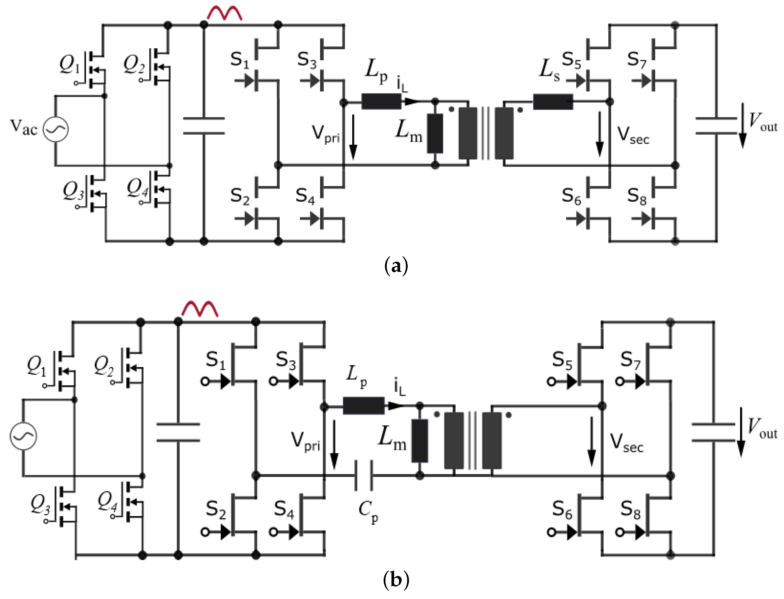
Dual Active Bridge (DAB) DC/DC Converter
The DAB, shown in Figure 19a, is a well-known topology that has been in use for a few decades [133] for bi-directional isolated DC/DC converter applications due to its high efficiency, high power density, soft switching possibility, and wide range of voltage transfer ratios [3,109,134]. As opposed to the resonant counterpart [90], the DAB [135] has a simpler structure since it does not require a series capacitor bank, which may occupy considerable space. However, due to the non-ideal behaviors such as the discrepancies among driver propagation delay characteristics, variations in the terminal voltage, and the dynamic operational phase-shift variations, the DC-bias becomes a challenging problem in practical applications [136]. That is why practical DAB applications may also employ a low voltage DC-blocking capacitor in series with the transformer winding to block the DC voltage component which will degrade the power density [135,136]. As a remedy, several active flux control methods have been proposed in the literature [136,137], which eliminates the use of series capacitors and the DC-bias current problem both during the transient and steady-state conditions. Conventionally, DAB employs only one external inductor on any side of the transformer [82]; however, as reported in [138] the inter-winding stray capacitance can cause current resonance and finally worsen soft switching in case of simultaneous switching events in both sides of the transformer. It is shown that splitting the external inductance to both sides of the high-frequency transformer can effectively extend the ZVS for all the switching devices [138]. Finally, DAB allows modular structures [99] to scale up to the higher power level thanks to its outstanding feature that paralleling can be easily achieved, as opposed to resonant topologies [3]. Therefore, by following a modular design approach, light load operation duration can be minimized by shedding some parallel units for efficiency optimization [5]. Unfortunately, Performance of a 5 kW rated GaN-based DAB DC/DC converter in a 400 V battery charging application has been demonstrated in [135]. Reportedly, this design has a maximum efficiency of 98.7% while operating at half power and 98% at rated power. Although this study provides valuable information on the magnetic components’ volume, unfortunately, it lacks details on the power density.
The half-bridge variant (DAHB) of DAB, shown in Figure 19b, for PHEV charging application utilizing GaN transistors has been presented in [139]. This configuration has the advantage of low transistor count with the compromise of reduced efficiency resulting from a transformer operation with half of the DC-link voltage. Therefore, this topology can be disadvantageous for high power, i.e., 22 kW, OBC applications. Another variant with a three-level ANPC half-bridge at the primary and secondary side is given in
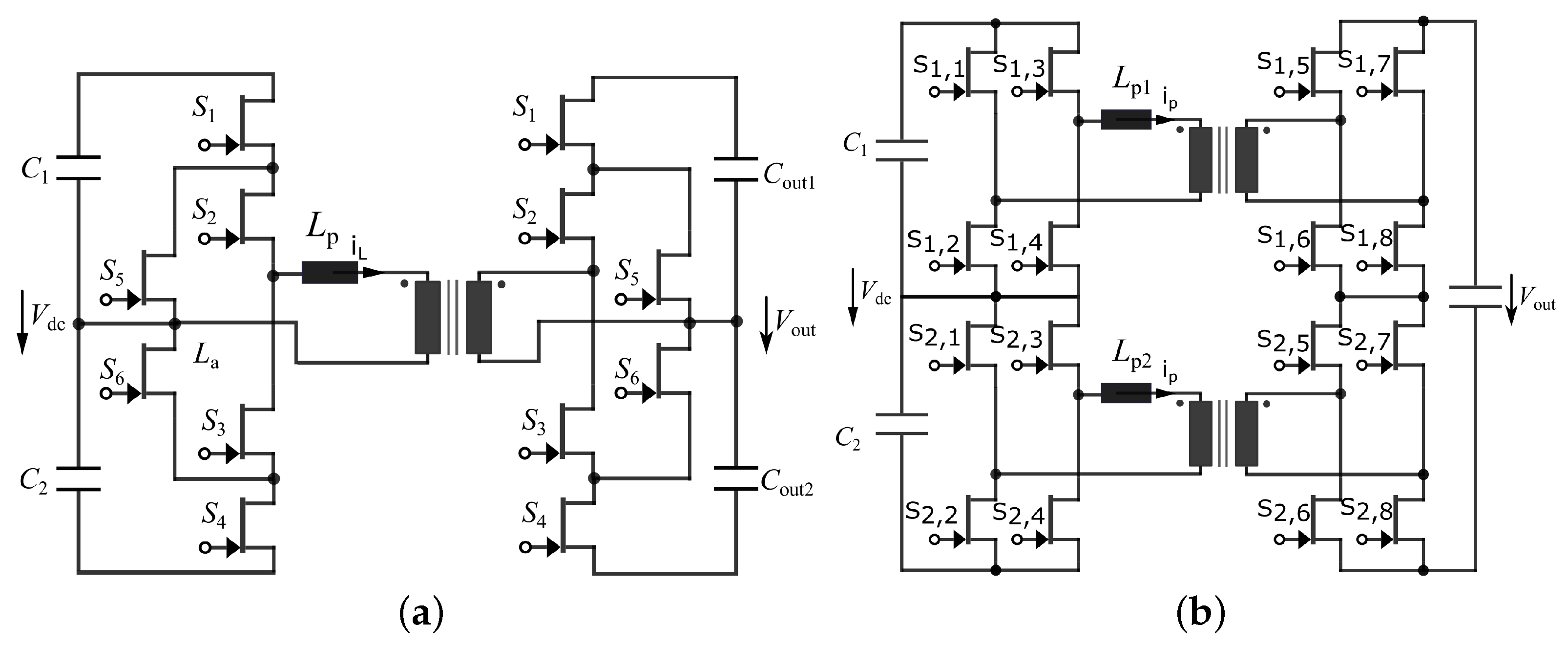
 Figure 20a [137], which is proposed for 800 V EV charging applications. In this work, the proposed three-level DAHB converter achieves a peak efficiency of 98.25% for an experimental prototype with a power rating of 1.5 kW. An additional option with a 10 kW power rating is the series-input, series-output (SISO) DAB converter, shown in Figure 20b, proposed in the recent study [99]. This converter is capable of functioning over a broad output voltage range of 250 V to 1000 V. While the efficiency of this converter is not stated in the study, it shows an impressive power density of 10 kW/L, including the AFE stage.
The DAB topology, while advantageous in many ways, is not without its limitations. One of the significant disadvantages of this topology is that its efficiency may fall below 90% under light load [82], mainly due to the absence of soft-switching and the persisting core losses with a subtle reduction from full load operation.
  • DAB Modulation Methods
In the DAB converter, bidirectional power flow is achieved by controlling the phase shift angle between the voltage waveforms of the two bridges [99]. Modulation techniques for the DAB topology have been thoroughly investigated in the literature [87,133,140,141,142,143,144]. The most well-known and simplest modulation method is named single-phase-shift (SPS) [133,140], in which, primary and secondary bridges are operated with 50% duty cycle, and only their phase difference is controlled to regulate the power flow. Power is sourced from the side modulated with a leading phase angle. Switching the polarity of the phase shift angle enables reverse power flow, and hence, the bidirectional operation can easily be achieved. While operating above one-third of the rated power with input/output voltages close to their nominal values, the SPS modulation achieves ZVS operation and high efficiency. The two basic ZVS requirements state that the inductor current i L should be flowing through the reverse conduction path of the upcoming switch which will take over the current and should be higher than a certain level to ensure charge and discharge the output capacitances of commutating transistors [125]. The ZVS range of DAB is also affected by the utilized dead-band as it ought be set larger than the ZVS resonance transient interval which depends on auxiliary inductor Lp and GaN transistor parasitic capacitances [87]. With these constraints, SPS requires a high auxiliary inductance Lp, cf. Figure 19a, to preserve ZVS ability at light load, resulting in high-circulating power and low efficiency for the DAB converter [133,140].
Various modulation methods have been proposed to address the efficiency issues of the SPS-modulated DAB topology at light loads. One approach is extended-phase shift (EPS) modulation [87], which allows for increased control degrees of freedom by operating one side of the converter below 50% duty cycle while the other side remains at 50%. Alternatively, dual-phase-shift (DPS) modulation [142] reduces the duty cycle of both sides to below 50%. Another method is triple-phase-shift (TPS) modulation, as discussed by Huang et al. and Chen et al. [143,145], which achieves greater control flexibility than other symmetrical modulations by using different duty cycles for both full-bridges. TPS includes two well-known sub-forms, namely the triangular (TRM) and trapezoidal modulation methods, whose names comes from the inductor current shape [134,141]. TRM provides a discontinuous conducting mode at light load with minimal rms current by reducing the circulating currents. However, for only two of the switches, ZVS turn-on is achieved [144] as far as the minimum commutation current needed for the resonant transition is available while the rest turns-on under zero current. However, turn-on under zero current, unfortunately, does not mean soft switching, and in fact, turn-on loss can account for as high as 30% of its nominal current value caused by the E o s s losses of high-side and low-side transistors [146].
As an alternative to the symmetrical modulation methods explained above, by bringing another degree of freedom to the modulator, recently a few asymmetrical modulation methods have been proposed [144,147]. In [147], the duty cycle of the low-voltage side is fixed at 50%, while the other side is operated at a lower duty cycle without following the half wave symmetry. Reportedly, the proposed approach has better ZVS performance, although full ZVS operation is not possible when compared to SPS, DPS, and EPS modulation methods under light load. However, the comparison does not include TRM and TPS modulation methods, and a circulating current is observable on transformer windings during the inactive mode. On the other hand, [144] presents a hybrid approach by combining EPS, SPS, and a new asymmetrical modulation to minimize rms current while guaranteeing the ZVS operation over a wide range. In their proposal, EPS is modified such that half wave symmetry is violated in a way that transformer winding volt-second balance is not stated. Therefore, this method requires an additional series blocking capacitor.
Depending on the transferred power and input/output voltage levels, the number of operating modes can be as many as twelve for TPS [125], and it is challenging to obtain the global optimal TPS parameters with three degrees of freedom. The same level of difficulty is also apparent for asymmetrical modulation methods. Several optimization studies have been proposed in the literature [87,134,142,143], and a review of other studies has been presented in [141]. The optimum modulation parameters can be obtained via different objective functions such as minimization of peak current stress [143] and rms values of the primary and secondary side currents [125,143,144], reactive power, i.e., circulating current [141] or total converter losses [134] with the constraint of achieving ZVS with different levels of complexities specific to the selected approach.
In DAB topology, both transferred power and circulating current also depend on switching frequency as well as the applied phase shift. Therefore, in addition to the phase-shift modulation methods, manipulation of modulation frequency is another viable approach to ensure ZVS over a wide power range with optimal circulating current [133,134,141]. Obviously, the switching frequency range is not infinite due to transformer saturation, core losses, and frequency-dependent skin/proximity effects on winding losses. Additionally, a wide switching frequency range aggravates the filter design and component choices. Finally, as implemented in [137] (DPS in their case), the presented modulation techniques are also applicable to multi-level DAB topologies.
Practically, these parameters (i.e., the duty-cycles, the phase-shift angle, and the dead times if adaptive dead-time is implemented) are pre-calculated for possible operating modes and stored as lookup tables in non-volatile memory to be used in the closed-loop control of the DAB converter [125]. However, as the loss of ZVS can increase losses tremendously, sensitivity analysis against variation of circuit parameters, e.g., inductance and transistor output capacitance, should be conducted and necessary actions should be taken. A large memory is needed to store enough data to cover all possible circuit parameter drift range. This may favor online calculation of global optimal modulation parameters by using closed form equations for some applications, as explained in [143]. A summary of prominent DAB modulation techniques is given in Table 9.
(b)
Resonant Dual-Active-Bridge DC/DC Converter Topologies
  • Resonant DAB topologies for the 400 V OBC Applications
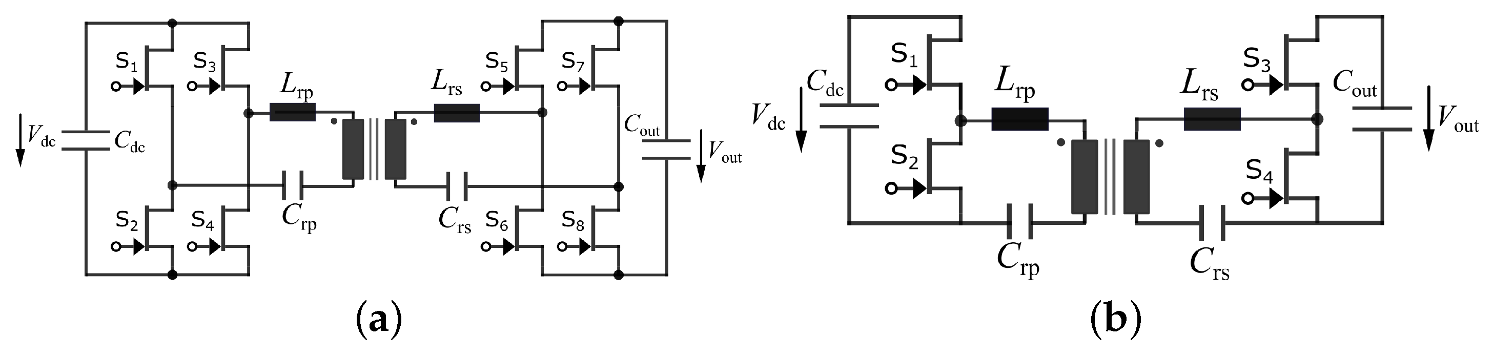
Unidirectional series resonant isolated converter, i.e., LLC, [149,150] is a well-known DC/DC topology for power electronic applications thanks to its advantages of soft switching and accompanying high-frequency operation capability, high efficiency, and good EMI performance. When the secondary side diodes are replaced with transistors, this topology can be also used for bidirectional charging applications [149]. However, in the reverse direction, i.e., in V2G mode, large turn-off currents are observed on the secondary side due to full AC-link current superimposed by the magnetizing current [149], and the efficiency drops towards the upper end of the output voltage range due to increased switching losses. To improve LLC performance for bidirectional power flow, another resonant tank is utilized in the secondary side of LLC topology resulting in CLLC topology as depicted in Figure 21a, providing similar characteristics in V2G and G2V modes [151]. Compared to the DAB converter, the CLLC converter is controlled by a variable switching frequency to regulate the voltage gain while achieving soft switching over a wider power range [3]. While operating in the vicinity of resonant frequency, a peak efficiency of 97.6% can be achievable for a CLLC converter designed for EV charging application utilizing 70 mΩ enhancement mode GaN transistors, with a variable switching frequency between 435 kHz and 575 kHz [152]. Results of this study show that semiconductor conduction losses occupy almost half of the overall converter losses due to intrinsic high rms currents occurring in a CLLC topology caused by the sinusoidal current shape. Nevertheless, by using high-current-rated devices, conduction losses can be reduced. In fact, for a similar rated CLLC using 34 mΩ GaN-GIT, a peak efficiency above 98% can be possible [59].
In [153], an isolated half-bridge CLLC converter, cf. Figure 21b, a prototype using 650 V GaN devices with a power rating of 1 kW has been demonstrated. This converter has a resonant frequency of 391 kHz. The most prominent advantage of this configuration is halved transistor count compared to the full-bridge CLLC. However, this increases the transformer winding losses and semiconductor conduction losses since the voltages are halved and the current is doubled compared to full-bridge CLLC with the same power rating. Although the demonstrated prototype operates with soft switching across the battery voltage range, it has a relatively low efficiency of up to 95.7% [153].
Table 10 compares the performance metrics of bi-directional GaN-based resonant DC/DC converter examples to an equivalent resonant converter demonstrated in [150]. The results indicate that incorporating bidirectional functionality does not necessarily decrease the efficiency or power density. On the contrary, bidirectional functionality can enhance both efficiency and power density. However, it is important to note that bidirectional topologies come with increased complexity, requiring additional power transistors and drivers for both resonant and non-resonant topologies as well as additional battery-side resonant tank components for resonant topologies. This added complexity may be considered a potential downside.
The CLLC topology exhibits serious design challenges to obtain a wide output voltage range [151]. In wide voltage range applications, a large resonant inductor is required to obtain a steep gain curve by increasing the Q factor to extend the regulation range [150]. However, a resonant tank with a large resonant inductor incurs high rms current and high peak voltage on the resonant capacitor. Furthermore, the switching frequency range also increases resulting in higher semiconductor and transformer losses. Above the resonant frequency, i.e., inductive region, circulating reactive current further increases the conduction losses [154] despite the soft switching being retained in which, switches operate in reverse conduction mode for longer duration. In this respect, Si- and SiC-based power transistors presents lower conduction loss thanks to contribution of body diode. That is why, use of GaN transistors in a CLLC converter with long operation time in this mode can be disadvantageous [155].
Table 10. Summary of GaN-based isolated DC/DC converter topologies for 400 V and 800 V EV applications.
TopologyYearPower RatingSwitch TypeModulationSwitching FrequencyPower DensityEfficiency (Peak/Full Load)Output Voltage
DAB HB [139]20223.3 kWGaNN/A100 kHzN/A95.04% (with PFC)72 V
DAB [135]20205 kWGaNDPS100 kHzN/A98.7%/98%400 V
CLLC [155]20173.3 kWHybrid (Si sec.)Frequency + Delay140–180 kHzN/A98%/97.4%400 V
GaN 97.4%/96.8%
Resonant LCL-T (pri. stacked HB, sec. FB) [94]20226.6 kWGaNPhase shift500 kHz7.3 kW/L98.2%/>97%400 V
CLLC [152]20223.3 kWGaNFrequency435–575 kHz7.9 kW/L97.6%/N/A400 V
CLLC Variable tap [59]20176 kWGaNN/AN/A3 kW/L (Including PFC unit)>98%/98%400 V
CLLC (fiexed gain) [156]202118 kWHybrid (SiC pri.)Fixed frequencyN/A8.7 kW/L>98.8%/N/A400 V
HB CLLC [153]20201 kWGaNFrequency391–500 kHzN/A95.7%/95.7%400 V
Resonant LCL-T (pri. and sec. stacked HB) [94]20226.6 kWGaNPhase shift500 kHz7.3 kW/L98.2%/>97.5%800 V
DAB (stacked) [99]202210 kWGaNHybrid (SPS+DPS)140–400 kHz10 kW/L (Including AFE)N/A250–1000 V
3-level DAHB [137]20223.3 kWGaNDPS100 kHzN/A>98.25%/N/A800 V
Hybrid LLC [150] (PSFB + LLC) *20203.2 kWGaN FB pri. and Si sec.Frequency modulation for both modes75–300 kHz4 kW/L98.5%/98.5%400 V
* Uni-directional converter is included for performance comparison.
To address the wide operating voltage requirement of the OBC applications, a possible solution could be a variable DC-link operation [90,156] for dual-stage architectures. Liu et al. compared the performance of conventional CLLC with variable DC-link operation [90], where an outstanding overall efficiency improvement, up to 1%, was achieved compared to fixed DC-link voltage operation. However, in this approach, DC-link is driven above typical commercial GaN voltage rating, i.e., 650 V, and thereby these applications typically utilize 1200 V SiC MOSFETs at the primary side. In another approach, input-parallel output-series (IPOS) isolated converter functions as a load-independent constant gain DC transformer (DCX) [156], allowing it to operate in the vicinity of the resonant frequency throughout the entire charging profile. This gives a flat efficiency profile for DC/DC stage optimized for best efficiency thanks to fixed voltage gain. Another partial power resonant converter was cascaded (cf. Figure 22b) with a non-isolated bi-polar bi-directional DC/DC converter assigned for battery voltage regulation. The two converters are supplied from a common 750 V DC-link, with the first one functioning as a fixed-gain DCX, which handles the majority of the power and the second one being responsible for output voltage regulation. This results in a peak efficiency of 98.8% and a relatively flat efficiency profile, excluding the light load conditions.
Several methods have been proposed to expand the output voltage range of the series resonant converters [59,150]. One of the most popular approaches is reconfigurable transformer taps to allow different transformer turns ratios; for example, ref. [59] shows reconfigurable turn ratios of 10:10 and 10:8 achieving an efficiency above 98% over a wide voltage range. The ZVS operating range can also be extended by applying hybrid modulation methods, which will be elaborated in the following section. Finally, there are a few studies proposing adjustable resonant tank parameters allowing resonant operation for different battery voltages [157], and reconfigurable unidirectional LLC converters [150], allowing resonant and phase-shifted full-bridge or half-bridge and full-bridge operation mode transitions. However, according to the best search of the authors, no such study has been found on GaN transistors that adopted this approach for bi-directional OBC application. Nevertheless, these approaches can also be extended to bi-directional CLLC topology [158].
  • Resonant DAB converters for 800 V OBC Applications
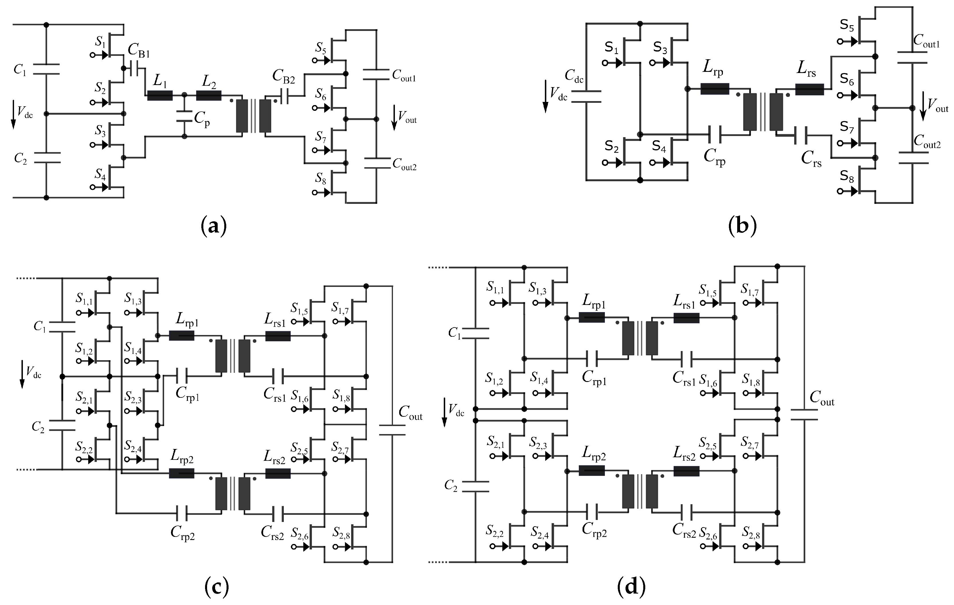
Finally, multi-winding transformer-based stacked isolated converters are drawing attention [99,100,106,159] for solid-state transformer (SST), DC micro-grid, and battery charging applications, especially 800 V systems, as well. In [94], the authors have proposed a resonant stacked half-bridge converter based on an LCL-T immittance network which operates at fixed 500 kHz switching frequency fed from a 800 V front-end converter. This converter can produce output voltages from 150 V up to 950 V. The measured converter achieves a peak efficiency of 98.2% along with a power density of 7.3 kW/L. Although this converter maintains a flat efficiency profile above > 97% across the whole output voltage range, at rated power, the light load efficiency falls below 90% like the two-level DAB and CLLC counterparts. The tuned LCL-T network presents a high impedance to harmonics generated by the converters, and therefore, the primary and secondary switch and transformer waveforms are approximately sinusoidal, minimizing the reactive power requirement of the converter irrespective of the load. The direction and magnitude of power flow is regulated by controlling the pulse width of primary and secondary side switching pattern (three-level modulation) while keeping the phase shift constant. Since this architecture does not have a series capacitor in its original form, additional dc blocking capacitors are required in both primary and secondary side due to uni-polar exciting voltages of stacked half-bridge. Exclusion of secondary side resonant network can outweigh the volume increase caused by the use of an additional inductor with similar sizing with the one used in CLLC converter. Although performance and switching behavior has been thoroughly analyzed for CC/CP/CV charging modes, the ZVS operation range is not detailed for V2G mode in this study. Since the magnetizing inductance can be designed significantly higher [94] than conventional LLC converter, problems evident in LLC reverse-mode operation [149] may not appear in this topology.
A few alternative conceptual topologies are shown in Figure 22b–d and Figure 23d based on multiple transformers and have been recommended in [106]. In case of a 400 V DC-link, ref. [106] proposes the topology given in Figure 22b for 800 V EV systems. An important advantage of this approaches is the re-configuring capability of the output circuit for parallel operation, as shown in Figure 23d for 400 V EV systems, despite the fact that paralleling of resonant converters is a challenging task [3]. Unfortunately, experimental studies issuing the performance evaluation of these topologies are very limited or not available yet. A stacked structure for 800 V charging application can be formed by connecting the two half-bridges in series [106,160], as shown in Figure 22b. Table 10 presents a summary of the comparison between GaN-based isolated DC/DC topologies for 400 and 800 V EV charging applications, with a particular focus on power density and efficiency. Finally, the table incorporates information on the modulation techniques used in each topology.
  • CLLC Modulation Techniques
Basic modulation of CLLC converter is known as pulse frequency modulation (PFM) technique [111], which is based on the DC gain characteristics of the resonant converter practically obtained by fundamental harmonic analysis (FHA) [161]. In this modulation technique, the timing of rectifying bridge gate signals has a crucial role to achieve ZCS at the secondary side [152], which necessitates employment of carefully tuned and sensitive zero crossing detection circuits. Dead-time optimization, depending on the loading, is also needed including the effect of GaN transistor output capacitance and the circuit parasitic capacitances [162,163]. Ref. [161] proposes a specialized version of frequency modulation to implement synchronous rectification of secondary side switches without using sensors. As stated in the previous section, this technique has significant disadvantages when applied to wide input/output voltage range applications. In order to address these limitations, numerous alternative techniques have been proposed in the literature, a summary of which is presented in Table 11.
Among them, the half-bridge mode implements a unipolar switching pattern at the primary side. This method reduces the switching speed by half, although the converter still operates at resonant frequency. Additionally, since half of the input voltage is blocked on the resonant capacitor, the fundamental component of the applied voltage is half of its nominal value [160]. However, in an EV charging application, converter output current is maximum when battery voltage is low in a CC/CV or CC/CP/CV charging profile [32,94,154]; thus, optimum efficiency may not be attained as the converter operates with a reduced effective input voltage. The burst mode [151] operation, on the other hand, is the intermittent operation of the converter during the light load conditions while being still excited typically at the frequency providing the best efficiency.
Delay time control [151,155] is another approach targeting extension of operation voltage range. In this method primary side is operated like in basic frequency modulation. On the other hand, secondary side HB legs, displaced by a phase difference above 180°, results in a state shorting the secondary side winding. This boost behavior [151] provides a higher output voltage compared to the conventional frequency control. This mode is typically only applied in the high output voltage CV region, which elevates circuit performance by enabling selection of a larger magnetizing inductance and higher turns ratio to reduce the conduction losses.
In contrast, when the primary side HB leg gate signals are displaced by a phase angle different from 180°, a new modulation technique known as inner phase-shift control (IPS) is obtained [165]. By controlling the phase shift between the primary side bridge legs, the output voltage can be regulated. Moreover, the primary side zero voltage switching, and secondary side zero current switching features are also ensured. Although the resulting mode is a step-down mode (if transformer turns ratio is equal to 1:1), it can replace the above resonance operation of PFM modulation, narrowing the switching frequency range significantly and eliminating the semiconductor turn-off losses which are inevitable for the above resonance operation [154].
The extended phase-shift (EPS) control [164], also known as the dual-phase-shift control technique [111], introduces an outer phase shift between primary and secondary bridges in addition to the IPS. Fundamental wave amplitude of the square wave voltage of the primary side bridge is adjusted by reducing the duty cycle below 50% to achieve high light load efficiency. Study [164] shows that by optimizing the phase-shift combinations for EPS control in the CLLC converter throughout the operation range, ZVS can be assured for both primary and secondary side switches. In practical applications, typically a hybrid modulation technique is adopted combining basic PFM and a phase-shift modulation [158] to optimize the converter design and reduce the operation frequency range.
The modulation techniques given in this study are also applicable to stacked CLLC converters [94,160]. Practically, a combination of two-level modulation [166] and three-level modulation can increase operation voltage range for multi-level resonant converters while achieving full range ZVS operation with reduced circulating current. For instance, in the low battery voltage range, [94] utilizes an asymmetrical modulation technique that alternates between the top and bottom half-bridges. This method leads to a switching frequency that is half of the resonant frequency. In normal operation, phase-shift modulation resulting in three-level waveforms is implemented. Notoriously, increasing degrees of freedom of stacked CLLC converters enables further extension of conventional modulation methods to achieve ZVS operation over a wide battery voltage range. However, this topic waits as future research, for now.
Table 12 illustrates how the choice of modulation method affects converter efficiency across the battery voltage range. By utilizing advanced modulation techniques, it is possible to achieve a flat efficiency profile throughout the charging process, specifically improving the light load performance, for both resonant and non-resonant isolated DC/DC converter topologies. Therefore, the impact of modulation technique on topology performance should not be overlooked.

6. Concluding Remarks and Future Research Trends

This section provides a comprehensive overview of the existing bi-directional OBC architectures that rely on GaN power transistors. Furthermore, projections regarding the possible transformations of applied architectures that could stem from the continued progress in GaN power transistor technology have been summarized. The two common structures, namely direct three-phase architecture and phase modular architecture of the EV on-board chargers have been discussed in this article. Both can be further sub-categorized as single-stage and dual-stage topologies. The state-of-the-art applicable OBC topologies are limited by the available commercial GaN power transistor glossary. Nevertheless, as the GaN technology matures, especially with the emergence of 1200 V rated [91] and/or bidirectional GaN power transistors, applicable topologies will widen. Among the existing applications, single-stage topologies stand out in terms of power density and circuit simplicity; with the imminent bidirectional GaN power transistors, they can revolutionize the application field, including high power use cases, i.e., 22 kW, as well. A noteworthy challenge of this approach is the limited degree of control freedom to achieve soft switching and low conduction losses, especially when additional functions, such as reactive power injection, which can be solely achieved by the AC/DC stage in a dual-stage implementation [23], are included.
Phase modular AC/DC topologies hold being the first choice in OBC applications thanks to modular nature and ease of paralleling for global compatibility. Although they require additional Si/SiC MOSFET as a folding/unfolding bridge, an associated gate driver with this additional low frequency half-bridge is a simple low-power driver [167], and power loss and cooling effort is not high. It is useful to compare the topologies based on the active switch utilization [168] factor, which is expressed as P s w i t c h / P o , where P s w i t c h is a benchmark factor being equal to the product of the peak voltage applied to semiconductor switch, and the rms current flowing through it. According to [168], as the switch utilization increases, the converter efficiency increases, while its cost decreases. When compared to direct three-phase systems, phase modular PFC topology with folding leg provides a better switch utilization by a factor of more than two times [100].
Implementation of GaN-based conventional direct three-phase, in other words, non-phase modular configurations requires use of multilevel topologies with the currently available GaN transistors and additional modifications for single-phase charging allowance. With wider availability of 1200 V GaN power transistors, OBC AC/DC stages may experience significant impacts. Specifically, single-phase use of two-level three-phase AFE topologies can be achieved with either a fourth leg or mechanical switches, leading to a decrease in component count. This has the potential to make these topologies the dominant choice for AC/DC stages in OBC applications.
An important remark for both phase modular and direct three phase AC/DC converter stages is the reduction of inductor volume thanks to GaN utilization, which may be outweighed by the required volume for 2nd harmonic power decoupling capacitors (to enable single-phase comaptibilty) and the EMI filter stage. Although the switching frequency can be driven well beyond MHz range in an OBC application, electrolytic capacitors inevitably are used for single-phase operation, hindering the power density improvement anticipated from GaN utilization in AC/DC stage. Thereby, innovative active power decoupling techniques [115] and optimized EMI filter designs [4,13] with properly tuned modulation methods can help to improve power density to make the best use of GaN utilization.
A thorough examination has been performed on the relevant applicable isolated converter topologies for the DC/DC power stage. DAB is the first topology that springs to mind for bidirectional operation, the power flow control of which is controlled by changing the phase shift between primary and secondary side modulation signals. With the use of advanced modulation techniques, such as TPS modulation, the DAB converter can achieve soft switching for a very wide operating voltage range. Easy scaling of power rating with paralleling is another benefit of this topology. However, the circulating (reactive) current and associated conduction losses of semiconductors and transformer necessitates a careful component optimization, including modulation. The DAB resonant, or CLLC, converter is another attractive alternative for isolated DC/DC converter stages, enabling soft switching over the complete range of EV battery voltage in a properly tuned design. Although GaN has unrivalled switching performance, outstanding reduction of switching losses via soft switching is still important for best-in-class efficiency and EMI performance. However, this topology excels DAB only if it operates slightly above resonant frequency. When combined with variable DC-link operation strategy, and by operating as a fixed gain DCX converter, CLLC is a feasible straight choice for many applications. Finally, associated modulation techniques with the presented topologies have also been reviewed since they are decisive on converter performance as much as the selected converter topology.
The research efforts should be carried out systematically and efficiently considering the several constraints, e.g., power density, safety, reliability, cost, and environmental impacts, in front of the successful growth and adoption of EV technology while seeking methods to attain an OBC short term efficiency target of 98% [28] and beyond. To reach this target, implementing partial power converters [28,156] and semiconductor-based galvanic isolation [96] can be a game-changer, even in the present time.
Given that the SOC HB solutions [67] are realized, we can anticipate a stellar performance from GaN-based converters in terms of these metrics thanks to higher switching frequencies enabled by improved layout. However, they will bring new challenges regarding thermal management since both transistors comprising the HB are confined in a small area. In this case, emerging dual sided cooling or immersion cooling methods [169,170] and can improve the thermal performance and heat dissipation capability substantially and open new doors for optimization of electrical layouts to achieve high power density converters.
Ultra-compact chargers, enabled by evolving GaN technology, can allow portable DC chargers paired with every EV to eliminate the of on-board charger from EVs in the near future [3]. This can provide numerous benefits such as reduced EV cost, easier serviceability, and reduced gross vehicle weight. Most importantly, the rate of charge will no longer be limited by the power rating of the OBC. These chargers are meant to be hand-held with a small form factor, natural convection cooled (i.e., without fans) [3]. Filter design and controllers [4,13,115] should account for case of multiple cars being charged on the same AC feeder in the near future to ensure converter stability requirements [13] are met.
A well-known concern about EV charging is the negative impacts on the grid. As discussed for long time, smart charging should be implemented to reduce the peak demand on the distribution network in which charging behavior is changed based on peak demand, renewable source generation, dynamic pricing, and habits of EV owners [171,172]. V2G capable efficient chargers can boost renewable integration [5] as well, by providing several ancillary services such as grid back-up, peak shaving, and reactive power support and grid frequency regulation [23,127,171] with associated well known control methods, e.g., droop control and decoupled power control [109]. Finally, the stability of parallel operating multiple distributed generators has been discussed in several studies [173,174] which are also applicable to V2G chargers; nevertheless, the effects of stability requirements on design requirements need to be elaborated.

7. Conclusions

This article provides a comprehensive survey of the current status and upcoming advancements in GaN power transistor technology as it applies to on-board charging (OBC) in electric vehicles (EVs). The application requirements are taken into consideration as well as a summary of the associated standards. Practical issues and concerns regarding the use of GaN transistors are also discussed. The state-of-the-art power converter topologies for on-board chargers used in 400 V and emerging 800 V EV systems are reviewed, along with key performance metrics and future predictions of implemented approaches. A categorization of these topologies is presented which comprises combinations of three-phase AFE and phase-modular single/dual-stage two-level and multilevel topologies suitable for OBC applications. Finally, a comparative evaluation of these topologies is carried out, including their merits and demerits in terms of various parameters such as variation of efficiency over charging profile, switching frequency range, ability to adapt a wide voltage range, complexity, and reliability aspects. The efficiency and power density of the OBC greatly depend on the converter topology implemented, which in turn affects the bi-directional charger acceptance, cost, and reliability objectives. Additionally, determining the optimal topology is contingent upon the user’s priorities and objectives as well as the efficiency zone being targeted, which may encompass all power levels or a specific point of interest. As such, this paper serves as a valuable resource for researchers and engineers seeking to study, design, and implement on-board chargers for EVs. The presented topologies are complemented by a glossary of applied low-level control techniques providing a comprehensive reference for practitioners in the field.

Funding

This work was supported by project Highly EFFICIENT and reliable electric drivetrains based on modular, intelligent, and highly integrated wide bandgap power electronics modules. This project has received funding from the ECSEL Joint Undertaking (JU) under grant agreement no. 101007281. The JU receives support from the European Union’s Horizon 2020 research and innovation programme and Austria, Germany, Slovenia, The Netherlands, Belgium, Slovakia, France, Italy, and Turkey.

Data Availability Statement

Not applicable.

Acknowledgments

Authors acknowledge Flanders Make for the support to this research group.

Conflicts of Interest

The authors declare no conflict of interest.

References

  1. BloombergNEF. Electric Vehicle Outlook 2022. Available online: https://iea.blob.core.windows.net/assets/e0d2081d-487d-4818-8c59-69b638969f9e/GlobalElectricVehicleOutlook2022.pdf (accessed on 10 August 2022).
  2. Gregoir, L.; Van Acker, K. Metals for Clean Energy: Pathways to solving Europe’s raw materials Challenge. Available online: https://eurometaux.eu/media/jmxf2qm0/metals-for-clean-energy.pdf (accessed on 6 February 2023).
  3. Harish, R.; Rangaraju, J. Power Topology Considerations for Electric Vehicle Charging Stations; Texas Instruments, Canadian Automobile Association: Kanata, ON, Canada, 2020; pp. 1–6. [Google Scholar]
  4. Papamanolis, P.; Krismer, F.; Kolar, J.W. 22 kW EV Battery Charger Allowing Full Power Delivery in 3-Phase as well as l-Phase Operation. In Proceedings of the ICPE 2019—ECCE Asia—10th International Conference on Power Electronics—ECCE Asia, Busan, Republic of Korea, 27–31 May 2019. [Google Scholar]
  5. Midhat, M. Paving the Way: Vehcile-to-Grid (V2G) Standards for Electric Vehicles. Available online: https://irecusa.org/wp-content/uploads/2022/01/Paving_the_Way_V2G-Standards_Jan.2022_FINAL.pdf (accessed on 15 July 2022).
  6. Manh Tran, T.; Zhaksylyk, A.; Abdel-Monem, M.; Rasool, H.; El Baghdadi, M.; Hegazy, O. Modeling and Control Algorithm for a Modular GaN On-Board Charging System in Automotive Applications. In Proceedings of the 2021 23rd European Conference on Power Electronics and Applications, EPE 2021 ECCE Europe, Ghent, Belgium, 6–10 September 2021; pp. 1–6. [Google Scholar]
  7. Grand View Research. Gallium Nitride Semiconductor Devices Market Size, Share and Trends Analysis Report by Product, by Component, by Wafer Size, by End Use, by Region, And Segment Forecasts, 2022–2030. Available online: https://www.researchandmarkets.com/reports/4452080/gallium-nitride-semiconductor-devices-market (accessed on 1 September 2022).
  8. Ashourloo, M.; Zaman, M.S.; Nasr, M.; Trescases, O. Opportunities for Leveraging Low-Voltage GaN Devices in Modular Multi-Level Converters for Electric-Vehicle Charging Applications. In Proceedings of the 2018 International Power Electronics Conference, IPEC-Niigata—ECCE Asia 2018, Niigata, Japan, 20–24 May 2018; pp. 2380–2385. [Google Scholar] [CrossRef]
  9. Lidow, A.; Strydom, J.; de Rooij, M.; Reusch, D. GaN Transistors for Efficient Power Conversion, 3rd ed.; Wiley: Hoboken, NJ, USA, 2020; Volume 9781118844, pp. 1–250. [Google Scholar] [CrossRef]
  10. Dusmez, S.; Ye, Z. Designing a 1kW GaN PFC stage with over 99% efficiency and 155W/in3 power density. In Proceedings of the 2017 IEEE 5th Workshop on Wide Bandgap Power Devices and Applications, WiPDA 2017, Albuquerque, NM, USA, 30 October–1 November 2017; pp. 225–232. [Google Scholar] [CrossRef]
  11. Inc, D. 7.4 kW Vehicle-to-Everything (V2X) Onboard Charger. Available online: https://diamond-us.com/7-4-kw-vehicle-to-everything-v2x-onboard-charger (accessed on 1 September 2022).
  12. Pushpakaran, B.N.; Subburaj, A.S.; Bayne, S.B. Commercial GaN-Based Power Electronic Systems: A Review. J. Electron. Mater. 2020, 49, 6247–6262. [Google Scholar] [CrossRef]
  13. Wyss, J.; Biela, J. Optimized Bidirectional PFC Rectifiers Inverters - Si vs. SiC vs. GaN in 2L and 3L Topologies -. In Proceedings of the 2018 International Power Electronics Conference, Niigata, Japan, 20–24 May 2018; pp. 3734–3741. [Google Scholar] [CrossRef]
  14. Su, G.J. Comparison of Si, SiC, and GaN based Isolation Converters for Onboard Charger Applications. In Proceedings of the 2018 IEEE Energy Conversion Congress and Exposition, ECCE 2018, Portland, OR, USA, 20–22 September 2018; pp. 1233–1239. [Google Scholar] [CrossRef]
  15. Keshmiri, N.; Wang, D.; Agrawal, B.; Hou, R.; Emadi, A. Current Status and Future Trends of GaN HEMTs in Electrified Transportation. IEEE Access 2020, 8, 70553–70571. [Google Scholar] [CrossRef]
  16. Jones, E.A.; Wang, F.F.; Costinett, D. Review of Commercial GaN Power Devices and GaN-Based Converter Design Challenges. IEEE J. Emerg. Sel. Top. Power Electron. 2016, 4, 707–719. [Google Scholar] [CrossRef]
  17. Ma, C.T.; Gu, Z.H. Review of GaN HEMT applications in power converters over 500 W. Electronics 2019, 8, 1401. [Google Scholar] [CrossRef] [Green Version]
  18. Yadlapalli, R.T.; Kotapati, A.; Kandipati, R.; Balusu, S.R.; Koritala, C.S. Advancements in energy efficient GaN power devices and power modules for electric vehicle applications: A review. Int. J. Energy Res. 2021, 45, 12638–12664. [Google Scholar] [CrossRef]
  19. Vecchia, M.D.; Ravyts, S.; den Broeck, G.V.; Driesen, J. Gallium-nitride semiconductor technology and its practical design challenges in power electronics applications: An overview. Energies 2019, 12, 2663. [Google Scholar] [CrossRef] [Green Version]
  20. Huang, Q.; Huang, A.Q. Review of GaN Totem-Pole Bridgeless PFC. CPSS Trans. Power Electron. Appl. 2017, 2, 187–196. [Google Scholar] [CrossRef]
  21. Yilmaz, M.; Krein, P.T. Review of battery charger topologies, charging power levels, and infrastructure for plug-in electric and hybrid vehicles. IEEE Trans. Power Electron. 2013, 28, 2151–2169. [Google Scholar] [CrossRef]
  22. Khalid, M.; Ahmad, F.; Panigrahi, B.K.; Al-Fagih, L. A comprehensive review on advanced charging topologies and methodologies for electric vehicle battery. J. Energy Storage 2022, 53, 105084. [Google Scholar] [CrossRef]
  23. Khaligh, A.; Dantonio, M. Global Trends in High-Power On-Board Chargers for Electric Vehicles. IEEE Trans. Veh. Technol. 2019, 68, 3306–3324. [Google Scholar] [CrossRef]
  24. Rivera, S.; Kouro, S.; Vazquez, S.; Goetz, S.M.; Lizana, R.; Romero-Cadaval, E. Electric Vehicle Charging Infrastructure: From Grid to Battery. IEEE Ind. Electron. Mag. 2021, 15, 37–51. [Google Scholar] [CrossRef]
  25. Sahinler, G.B.; Poyrazoglu, G. V2G Applicable Electric Vehicle Chargers, Power Converters Their Controllers: A Review. In Proceedings of the 2020 IEEE 2nd Global Power, Energy and Communication Conference, GPECOM 2020, Izmir, Turkey, 20–23 October 2020; pp. 59–64. [Google Scholar] [CrossRef]
  26. Subotic, I.; Levi, E. A review of single-phase on-board integrated battery charging topologies for electric vehicles. In Proceedings of the 2015 IEEE Workshop on Electrical Machines Design, Control and Diagnosis, WEMDCD 2015, Torino, Italy, 20–24 May 2015; pp. 136–145. [Google Scholar] [CrossRef]
  27. Yuan, J.; Dorn-Gomba, L.; Callegaro, A.D.; Reimers, J.; Emadi, A. A review of bidirectional on-board chargers for electric vehicles. IEEE Access 2021, 9, 51501–51518. [Google Scholar] [CrossRef]
  28. Rivera, S.; Member, S.; Rojas, J.; Kouro, S.; Member, S.; Lehn, P.W.; Member, S.; Lizana, R.; Member, S.; Renaudineau, H.; et al. Partial-Power Converter Topology of Type II for Efficient Electric Vehicle Fast Charging. IEEE J. Emerg. Sel. Top. Power Electron. 2021, 6777, 1–10. [Google Scholar] [CrossRef]
  29. Gaona-Cárdenas, L.F.; Vázquez-Nava, N.; Ruíz-Martínez, O.F.; Espinosa-Calderón, A.; Barranco-Gutiérrez, A.I.; Rodríguez-Licea, M.A. An Overview on Fault Management for Electric Vehicle Onboard Chargers. Electronics 2022, 11, 1107. [Google Scholar] [CrossRef]
  30. Jaman, S.; Chakraborty, S.; Tran, D.d.; Geury, T.; Baghdadi, M.E.; Hegazy, O. Review on Integrated On-Board Charger-Traction Systems: V2G Topologies, Control Approaches, Standards and Power Density State-of-the-Art for Electric Vehicle. Energies 2022, 15, 5376. [Google Scholar] [CrossRef]
  31. Bahrami, A. EV Charging Definitions, Modes, Levels, Communication Protocols and Applied Standards. Changes 2020, 1, 1–10. [Google Scholar]
  32. IEC 61851-1:2019; Electric Vehicle Conductive Charging System—Part 1: General Requirements. International Electrotechnical Commission (IEC): Geneva, Switzerland, 2019.
  33. Van Den Peter, B.; Tom, T.; Noshin, O.; Van Joeri, M. Developments and challenges for EV charging infrastructure standardization. In Proceedings of the EVS 2016—29th International Electric Vehicle Symposium, Montreal, QC, Canada, 20–22 June 2016. [Google Scholar]
  34. Sfakianakis, G.E.; Everts, J.; Lomonova, E.A. Overview of the requirements and implementations of bidirectional isolated AC-DC converters for automotive battery charging applications. In Proceedings of the 2015 Tenth International Conference on Ecological Vehicles and Renewable Energies (EVER), Monte Carlo, Monaco, 31 March–5 April 2015; pp. 1–12. [Google Scholar]
  35. REFUdrive. OBC 22K BIPOWER. Available online: https://www.refu-drive.com/en/products/on-board-charger/ (accessed on 10 December 2022).
  36. Innoelectric. On-Board Charger. Available online: https://innolectric.ag/on-board-charger-2-2/?lang=en (accessed on 10 June 2022).
  37. Stengert, K. On-board 22 kW fast charger “nLG6”. In Proceedings of the 2013 World Electric Vehicle Symposium and Exhibition, EVS 27, Barcelona, Spain, 17–20 November 2013; pp. 1–11. [Google Scholar] [CrossRef]
  38. Rata, M.; Rata, G.; Filote, C.; Raboaca, M.S.; Graur, A.; Afanasov, C.; Felseghi, A.R. The electricalvehicle simulator for charging station in mode 3 of IEC 61851-1 standard. Energies 2019, 13, 176. [Google Scholar] [CrossRef] [Green Version]
  39. Mariscotti, A. Harmonic and Supraharmonic Emissions of Plug-In Electric Vehicle Chargers. Smart Cities 2022, 5, 496–521. [Google Scholar] [CrossRef]
  40. Goldammer, E.; Gentejohann, M.; Schlüter, M.; Weber, D.; Wondrak, W.; Dieckerhoff, S.; Gühmann, C.; Kowal, J. The Impact of an Overlaid Ripple Current on Battery Aging: The Development of the SiCWell Dataset. Batteries 2022, 8, 11. [Google Scholar] [CrossRef]
  41. Brand, M.J.; Hofmann, M.H.; Schuster, S.S.; Keil, P.; Jossen, A. The influence of current ripples on the lifetime of lithium-ion batteries. IEEE Trans. Veh. Technol. 2018, 67, 10438–10445. [Google Scholar] [CrossRef]
  42. Keil, P.; Jossen, A. Charging protocols for lithium-ion batteries and their impact on cycle life—An experimental study with different 18650 high-power cells. J. Energy Storage 2016, 6, 125–141. [Google Scholar] [CrossRef]
  43. De Breucker, S.; Engelen, K.; D’hulst, R.; Driesen, J. Impact of current ripple on Li-ion battery ageing. World Electr. Veh. J. 2013, 6, 532–540. [Google Scholar] [CrossRef] [Green Version]
  44. EN 61851-21-1:2017; Electric Vehicle Conductive Charging System—Part 21-1 Electric Vehicle on-Board Charger EMC Requirements for Conductive Connection to AC/DC Supply. International Electrotechnical Commission (IEC): Geneva, Switzerland, 2019.
  45. IEC. International Special Committee on Radio Interference (CISPR); Guidance for Users of the CISPR Standards; International Electrotechnical Commission (IEC): Geneva, Switzerland, 2021; pp. 1–20. [Google Scholar]
  46. Valente, M.; Wijekoon, T.; Freijedo, F.; Pescetto, P.; Pellegrino, G.; Bojoi, R. Integrated on-board EV battery chargers: New perspectives and challenges for safety improvement. In Proceedings of the 2021 IEEE Workshop on Electrical Machines Design, Control and Diagnosis, WEMDCD 2021, Torino, Italy, 22–26 May 2021; pp. 349–356. [Google Scholar] [CrossRef]
  47. Krein, P.T. Electrostatic discharge issues in electric vehicles. IEEE Trans. Ind. Appl. 1996, 32, 1278–1284. [Google Scholar] [CrossRef]
  48. Chakraborty, S.; Hasan, M.M.; Paul, M.; Tran, D.D.; Geury, T.; Davari, P.; Blaabjerg, F.; El Baghdadi, M.; Hegazy, O. Real-Life Mission Profile Oriented Lifetime Estimation of a SiC Interleaved Bidirectional HV DC/DC Converter for Electric Vehicle Drivetrains. IEEE J. Emerg. Sel. Top. Power Electron. 2021. [Google Scholar] [CrossRef]
  49. Mimura, T. The early history of the high electron mobility transistor (HEMT). IEEE Trans. Microw. Theory Tech. 2002, 50, 780–782. [Google Scholar] [CrossRef]
  50. Wolf, M.; Hilt, O.; Wurfl, J. Gate Control Scheme of Monolithically Integrated Normally off Bidirectional 600-V GaN HFETs. IEEE Trans. Electron Devices 2018, 65, 3878–3883. [Google Scholar] [CrossRef]
  51. Huang, Q.; Yu, R.; Ma, Q.; Huang, A.Q. Predictive ZVS Control with Improved ZVS Time Margin and Limited Variable Frequency Range for a 99% Efficient, 130-W/in 3 MHz GaN Totem-Pole PFC Rectifier. IEEE Trans. Power Electron. 2019, 34, 7079–7091. [Google Scholar] [CrossRef]
  52. Endruschat, A.; Novak, C.; Gerstner, H.; Heckel, T.; Joffe, C.; Marz, M. A Universal SPICE Field-Effect Transistor Model Applied on SiC and GaN Transistors. IEEE Trans. Power Electron. 2019, 34, 9131–9145. [Google Scholar] [CrossRef]
  53. Amano, H.; Baines, Y.; Beam, E.; Borga, M.; Bouchet, T.; Chu, R.; Santi, C.D.; Souza, M.M.D. The 2018 GaN power electronics roadmap. J. Phys. Appl. Phys. 2018, 51, 163001. [Google Scholar] [CrossRef]
  54. Gareau, J.; Hou, R.; Emadi, A. Review of Loss Distribution, Analysis, and Measurement Techniques for GaN HEMTs. IEEE Trans. Power Electron. 2020, 35, 7405–7418. [Google Scholar] [CrossRef]
  55. Xu, J.; Qiu, Y.; Chen, D.; Lu, J.; Hou, R.; Maso, P.D. An Experimental Comparison of GaN E-HEMTs versus SiC MOSFETs over Different Operating Temperatures. Bodo’s Power Syst. 2018. Available online: https://gansystems.com/wp-content/uploads/2018/03/An-Experimental-Comparison-of-GaN-E-HEMTs-versus-SiC-MOSFETs-over-Different-Operating-Temperatures.pdf (accessed on 1 July 2022).
  56. Frisch, M. SiC MOSFET-Based Power Modules Utilizing Split Output Topology for Superior Dynamic Behavior; Vincotech GmbH: Unterhaching, Germany, 2013; pp. 24–26. [Google Scholar]
  57. Taylor, A.; Lu, J.; Zhu, L.; Bai, K.; McAmmond, M.; Brown, A. Comparison of SiC MOSFET-based and GaN HEMT-based high-efficiency high-powerdensity 7.2 kW EV battery chargers. IET Power Electron. 2018, 11, 1–9. [Google Scholar] [CrossRef]
  58. Ishibashi, T.; Okamoto, M.; Hiraki, E.; Tanaka, T.; Hashizume, T.; Kikuta, D.; Kachi, T. Experimental Validation of Normally-On GaN HEMT and Its Gate Drive Circuit. IEEE Trans. Ind. Appl. 2015, 51, 2415–2422. [Google Scholar] [CrossRef]
  59. Endres, S.; Seßler, C.; Zeltner, S.; Eckardt, B.; Morita, T. 6 kW Bidirectional, Insulated On-board Charger with Normally- Off GaN Gate Injection Transistors. In Proceedings of the PCIM Europe 2017, International Exhibition and Conference for Power Electronics, Intelligent Motion, Renewable Energy and Energy Management, Nuremberg, Germany, 16–18 May 2017; pp. 16–18. [Google Scholar]
  60. Uemoto, Y.; Hikita, M.; Ishida, H.; Ueno, H.; Matsuo, H.; Yanagihara, M.; Ueda, T. Gate Injection Transistor (GIT)—A Normally-Off Conductivity Modulation. IEEE Trans. Electron Devices 2007, 54, 3393–3399. [Google Scholar] [CrossRef]
  61. Transphorm. 900V Cascode GaN FET in TO-247. Available online: https://www.transphormusa.com/en/product/tp90h050ws-2/ (accessed on 1 July 2022).
  62. Raheja, U.; Gohil, G.; Han, K.; Acharya, S.; Baliga, B.J.; Battacharya, S.; Labreque, M.; Smith, P.; Lal, R. Applications and characterization of four quadrant GaN switch. In Proceedings of the 2017 IEEE Energy Conversion Congress and Exposition, ECCE 2017, Cincinnati, OH, USA, 1–5 October 2017. [Google Scholar] [CrossRef]
  63. Vollmaier, F.; Nain, N.; Huber, J.; Kolar, J.W.; Leong, K.K.; Pandya, B. Performance Evaluation of Future T-Type PFC Rectifier and Inverter Systems with Monolithic Bidirectional 600 v GaN Switches. In Proceedings of the 2021 IEEE Energy Conversion Congress and Exposition, Virtual, 10–14 October 2021; pp. 5297–5304. [Google Scholar] [CrossRef]
  64. Li, X.; Geens, K.; Guo, W.; You, S.; Zhao, M.; Fahle, D.; Odnoblyudov, V.; Groeseneken, G.; Decoutere, S. Demonstration of GaN Integrated Half-Bridge with On-Chip Drivers on 200-mm Engineered Substrates. IEEE Electron. Device Lett. 2019, 40, 1499–1502. [Google Scholar] [CrossRef]
  65. Navitas. Nv6117 GaNFast™ Power IC. Available online: https://navitassemi.com/wp-content/uploads/2022/06/NV6117-Datasheet-FINAL-05-19-22.pdf (accessed on 29 June 2022).
  66. Dusmez, S.; Fu, L.; Beheshti, M.; Brohlin, P.; Gao, R. Overcurrent Protection in High-Density GaN Power Designs. Available online: www.ti.com (accessed on 10 June 2022).
  67. Decoutere, S. All-GaN GaN-ICs in the IMEC’ s GaN-on-SOI Technology. Available online: https://www.imec-int.com/en/innovation/build-your-gan-ics-with-imec-s-gan-on-soi-mpw-process/tutorial-gan-ics-in-gan-on-soi-technology (accessed on 18 October 2022).
  68. GaNPower International. GaNPower Demonstrates Industry’s First 1200 V Single-Die E-Mode GaN Power Devices. Available online: https://iganpower.com (accessed on 19 December 2022).
  69. Roig, J.; Gomez, G.; Bauwens, F.; Vlachakis, B.; Rodriguez, J.; Rogina, M.R.; Rodriguez, A.; Lamar, D.G. Series-connected GaN transistors for ultra-fast high-voltage switch (>1kV). In Proceedings of the IEEE Applied Power Electronics Conference and Exposition, Tampa, FL, USA, 26–30 March 2017; pp. 3043–3048. [Google Scholar] [CrossRef]
  70. Odyssey Semiconductor. Odyssey Semiconductor Achieves 1200 Volt Rating on Vertical GaN Power Devices. Available online: https://odysseysemi.com (accessed on 19 December 2022).
  71. Li, X.; Van Hove, M.; Zhao, M.; Geens, K.; Guo, W.; You, S.; Stoffels, S.; Lempinen, V.P.; Sormunen, J.; Groeseneken, G.; et al. Suppression of the backgating effect of enhancement-mode p-GaN HEMTs on 200-mm GaN-on-SOI for Monolithic Integration. IEEE Electron Device Lett. 2018, 39, 999–1002. [Google Scholar] [CrossRef]
  72. Businesswire. GaN Power Devices: Global Strategic Business Report. Available online: https://www.researchandmarkets.com/reports/5030659/gan-power-devices-global-strategic-business (accessed on 10 July 2022).
  73. McDonald, T. Reliability and Qualification of CoolGaN™ Technology and Devices. Available online: https://www.infineon.com/dgdl/Infineon-2_WhitePaper_Reliability_and_qualification_of_CoolGaN_EN-WP-v01_00-EN.pdf?fileId=5546d46266a498f50166c9bebef322aa (accessed on 8 October 2022).
  74. Nexperia. Circuit Design and PCB Layout Recommendations for GaN FET Half Bridges; NXP Semiconductors: Eindhoven, The Netherlands, 2019. [Google Scholar]
  75. Kozak, J.P.; Song, Q.; Zhang, R.; Liu, J.; Zhang, Y. Robustness of GaN Gate Injection Transistors under Repetitive Surge Energy and Overvoltage. In Proceedings of the 2021 IEEE International Reliability Physics Symposium (IRPS), Monterey, CA, USA, 21–25 March 2021; pp. 1–5. [Google Scholar] [CrossRef]
  76. Chen, J.; Luo, Q.; Wei, Y.; Zhang, X.; Du, X. The Sustained Oscillation Modeling and Its Quantitative Suppression Methodology for GaN Devices. IEEE Trans. Power Electron. 2021, 36, 7927–7941. [Google Scholar] [CrossRef]
  77. An Analytical Model for False Turn-On Evaluation of High-Voltage Enhancement-Mode GaN Transistor in Bridge-Leg Configuration. IEEE Trans. Power Electron. 2017, 32, 6416–6433. [CrossRef]
  78. Qian, W.; Lu, J.; Bai, H.; Averitt, S. Hard-Switching 650-V GaN HEMTs in an 800-V DC-Grid System with No-Diode-Clamping Active-Balancing Three-Level Topology. IEEE J. Emerg. Sel. Top. Power Electron. 2019, 7, 1060–1070. [Google Scholar] [CrossRef]
  79. Peterson, Z. Selecting Materials for High Voltage PCB Design and Layout. Available online: https://resources.altium.com/p/high-voltage-pcb-design-tips-materials-for-high-voltage-pcbs (accessed on 30 November 2022).
  80. Lu, J.; Tian, Q.; Bai, K.; Brown, A.; McAmmond, M. An indirect matrix converter based 97%-efficiency on-board level 2 battery charger using E-mode GaN HEMTs. In Proceedings of the WiPDA 2015 3rd IEEE Workshop on Wide Bandgap Power Devices and Applications, Blacksburg, VI, USA, 2–4 November 2015; pp. 351–358. [Google Scholar] [CrossRef]
  81. Pozo, A.; Zhang, S.; Stecklein, G.; Garcia, R.; Glaser, J.; Tang, Z.; Strittmatter, R.; Lidow, A. GaN Reliability and Lifetime Projections. Available online: https://epc-co.com/epc/design-support/gan-fet-reliability/reliabilityreportphase14 (accessed on 20 November 2022).
  82. Ramachandran, R.; Nymand, M. Experimental Demonstration of a 98.8% Efficient Isolated DC–DC GaN Converter. IEEE Trans. Ind. Electron. 2017, 64, 9104–9113. [Google Scholar] [CrossRef]
  83. Lyu, X.; Li, H.; Abdullah, Y.; Wang, K.; Hu, B.; Yang, Z.; Liu, J.; Wang, J.; Liu, L.; Bala, S. A Reliable Ultrafast Short-Circuit Protection Method for E-Mode GaN HEMT. IEEE Trans. Power Electron. 2020, 35, 8926–8933. [Google Scholar] [CrossRef]
  84. Karakaya, F.; Alemdar, O.S.; Keysan, O. Layout-Based Ultrafast Short-Circuit Protection. IEEE J. Emerg. Sel. Top. Power Electron. 2021, 9, 6385–6395. [Google Scholar] [CrossRef]
  85. Huang, Q.; Ma, Q.; Liu, P.; Huang, A.Q.; De Rooij, M.A. 99% Efficient 2.5-kW four-level flying capacitor multilevel GaN totem-pole PFC. IEEE J. Emerg. Sel. Top. Power Electron. 2021, 9, 5795–5806. [Google Scholar] [CrossRef]
  86. Long, X.; Jun, Z.; Pu, L.; Chen, D.; Liang, W. Analysis and Suppression of High Speed Dv/Dt Induced False Turn-on in GaN HEMT Phase-Leg Topology. IEEE Access 2021, 9, 45259–45269. [Google Scholar] [CrossRef]
  87. Shi, H.; Wen, H.; Hu, Y. Deadband Effect and Accurate ZVS Boundaries of GaN-Based Dual-Active-Bridge Converters with Multiple-Phase-Shift Control. IEEE Trans. Power Electron. 2020, 35, 9888–9905. [Google Scholar] [CrossRef]
  88. GanSystems. GS66508B, Bottom-Side Cooled 650 V E-Mode GaN Transistor. Available online: https://gansystems.com/wp-content/uploads/2021/12/GS66516B-DS-Rev-211025.pdf (accessed on 5 December 2022).
  89. Gabbar, H.A.; Othman, A.M.; Abdussami, M.R. Review of Battery Management Systems (BMS) Development and Industrial Standards. Technologies 2021, 9, 28. [Google Scholar] [CrossRef]
  90. Li, B.; Li, Q.; Lee, F.C.; Liu, Z.; Yang, Y. A high-efficiency high-density wide-bandgap device-based bidirectional on-board charger. IEEE J. Emerg. Sel. Top. Power Electron. 2018, 6, 1627–1636. [Google Scholar] [CrossRef]
  91. Aghabali, I.; Bauman, J.; Kollmeyer, P.J.; Wang, Y.; Bilgin, B.; Emadi, A. 800-V Electric Vehicle Powertrains: Review and Analysis of Benefits, Challenges, and Future Trends. IEEE Trans. Transp. Electrif. 2021, 7, 927–948. [Google Scholar] [CrossRef]
  92. Kim, J.Y.; Lee, B.S.; Kwon, D.H.; Lee, D.W.; Kim, J.K. Low Voltage Charging Technique for Electric Vehicles with 800 v Battery. IEEE Trans. Ind. Electron. 2022, 69, 7890–7896. [Google Scholar] [CrossRef]
  93. Vetrivelan, A.; Chen, Z.; Huang, Q.; Persson, E.; Huang, A.Q. Design and implementation of A 5kW 99.2% efficient high-density gan-based totem pole interleaved bridgeless bidirectional PFC. In Proceedings of the IEEE Applied Power Electronics Conference and Exposition-APEC, Virtual, 10–14 October 2021; pp. 1843–1847. [Google Scholar] [CrossRef]
  94. Mukherjee, S.; Ruiz, J.M.; Barbosa, P. A High Power Density Wide Range DC–DC Converter for Universal Electric Vehicle Charging. IEEE Trans. Power Electron. 2022, 38, 1998–2012. [Google Scholar] [CrossRef]
  95. Dong, A.; Sadeghpour, D.; Bauman, J. High Efficiency GaN-based Non-isolated Electric Vehicle On-board Charger with Active Filtering. In Proceedings of the 2022 IEEE Transportation Electrification Conference & Expo (ITEC), Anaheim, CA, USA, 15–17 June 2022; pp. 1307–1313. [Google Scholar]
  96. Yao, C.; Zhang, X.; Zhang, Y.; Yang, P.; Li, H.; Wang, J. Semiconductor-Based Galvanic Isolation: Touch Current Suppression. IEEE Trans. Power Electron. 2020, 35, 48–58. [Google Scholar] [CrossRef]
  97. Kanstad, T.; Lillholm, M.B.; Zhang, Z. Highly efficient EV battery charger using fractional charging concept with SiC devices. In Proceedings of the IEEE Applied Power Electronics Conference and Exposition-APEC 2019, Anaheim, CA, USA, 17–21 March 2019; pp. 1601–1608. [Google Scholar] [CrossRef] [Green Version]
  98. Kim, H.; Park, J.; Kim, S.; Hakim, R.M.; Belkamel, H. A Single-Stage Electrolytic Capacitor-Less EV Charger with Single- and Three-Phase Compatibility. IEEE Trans. Power Electron. 2022, 37, 6780–6791. [Google Scholar] [CrossRef]
  99. Kasper, M.J.; Anderson, J.A.; Deboy, G.; Li, Y.; Haider, M.; Kolar, J.W. Next Generation GaN-based Architectures: From 240W USB-C Adapters to 11kW EV On-Board Chargers with Ultra-high Power Density and Wide Output Voltage Range. PCIM Eur. Conf. Proc. 2022, 1, 4–13. [Google Scholar] [CrossRef]
  100. Anderson, J.A.; Zulauf, G.; Papamanolis, P.; Hobi, S.; Miric, S.; Kolar, J.W. Three Levels Are Not Enough: Scaling Laws for Multilevel Converters in AC/DC Applications. IEEE Trans. Power Electron. 2021, 36, 3967–3986. [Google Scholar] [CrossRef]
  101. Najjar, M.; Nymand, M.; Kouchaki, A. Efficiency Comparisons of Two-Level and Three-Level GaN/SiC Based Converters. In Proceedings of the Energy Conversion Congress and Exposition-Asia, ECCE Asia 2021, Singapore, 21–24 May 2021; pp. 13–18. [Google Scholar] [CrossRef]
  102. Schrittwieser, L.; Leibl, M.; Kolar, J.W. 99% Efficient isolated three-phase matrix-type DAB buck-boost PFC rectifier. IEEE Trans. Power Electron. 2020, 35, 138–157. [Google Scholar] [CrossRef]
  103. Varajao, D.; Araujo, R.E.; Miranda, L.M.; Lopes, J.A. Modulation Strategy for a Single-Stage Bidirectional and Isolated AC-DC Matrix Converter for Energy Storage Systems. IEEE Trans. Ind. Electron. 2018, 65, 3458–3468. [Google Scholar] [CrossRef]
  104. Kolar, J.W.; Huber, J.E. SiC/GaN 3-Φ PFC Rectifier/PWM Inverter Systems. In Proceedings of the ECCE Asia 2021, Singapore, 24–27 May 2021. [Google Scholar]
  105. Kolar, J.W. Potential GaN Bidirectional Switch Applications. Available online: https://www.pes-publications.ee.ethz.ch/uploads/tx_ethpublications/further_publications/__ETHZ_Bidirectional_GaN_Switch_Topologies_290618.pdf (accessed on 10 December 2022).
  106. Natarajan, R. Benefits of 650-Gan Fets for 800v-Power Converters. Available online: https://training.ti.com/benefits-650-v-gan-fets-800-v-power-converters (accessed on 10 July 2022).
  107. Najjar, M.; Kouchaki, A.; Nielsen, J.; Dan Lazar, R.; Nymand, M. Design Procedure and Efficiency Analysis of a 99.3% Efficient 10 kW Three-Phase Three-Level Hybrid GaN/Si Active Neutral Point Clamped Converter. IEEE Trans. Power Electron. 2022, 37, 6698–6710. [Google Scholar] [CrossRef]
  108. Syu, Y.L.; Liao, Z.; Fu, N.T.; Liu, Y.C.; Chiu, H.J.; Pilawa-Podgurski, R.C. Design and control of a high power density three-phase flying capacitor multilevel power factor correction rectifier. In Proceedings of the IEEE Applied Power Electronics Conference and Exposition-APEC, Virtual, 14–17 June 2021; pp. 613–618. [Google Scholar] [CrossRef]
  109. Safayatullah, M.; Elrais, M.T.; Ghosh, S.; Rezaii, R.; Batarseh, I. A Comprehensive Review of Power Converter Topologies and Control Methods for Electric Vehicle Fast Charging Applications. IEEE Access 2022, 10, 40753–40793. [Google Scholar] [CrossRef]
  110. Bai, H.; Brown, A.; McAmmond, M.; Lu, J. A Modular Designed Three-Phase 98%-Efficiency 5 kW/L On-Board Fast Charger for Electric Vehicles Using Paralleled E-Mode GaN HEMTs. SAE Tech. Pap. 2017, 2017, 1697. [Google Scholar] [CrossRef]
  111. Yang, D.; Zhang, Y.; Liu, X.; Wang, W.; Liu, J. Overview of CLLC Modulation Strategy. In Proceedings of the 2022 International Power Electronics Conference, IPEC-Himeji 2022-ECCE Asia, Himeji, Japan, 15–19 May 2022; pp. 1633–1640. [Google Scholar] [CrossRef]
  112. Krein, P.T.; Balog, R.S.; Mirjafari, M. Minimum energy and capacitance requirements for single-phase inverters and rectifiers using a ripple port. IEEE Trans. Power Electron. 2012, 27, 4690–4698. [Google Scholar] [CrossRef]
  113. Lahyani, A.; Venet, P.; Grellet, G.; Viverge, P.J. Failure prediction of electrolytic capacitors during operation of a switchmode power supply. IEEE Trans. Power Electron. 1998, 13, 1199–1207. [Google Scholar] [CrossRef] [Green Version]
  114. Zhao, H.; Shen, Y.; Ying, W.; Ghosh, S.S.; Ahmed, M.R.; Long, T. A Single- and Three-Phase Grid Compatible Converter for Electric Vehicle On-Board Chargers. IEEE Trans. Power Electron. 2020, 35, 7545–7562. [Google Scholar] [CrossRef]
  115. Gautam, A.R.; Fulwani, D.M.; Makineni, R.R.; Rathore, A.K.; Singh, D. Control Strategies and Power Decoupling Topologies to Mitigate 2ω-Ripple in Single-Phase Inverters: A Review and Open Challenges. IEEE Access 2020, 8, 147533–147559. [Google Scholar] [CrossRef]
  116. Gonçalves, J.T.; Valtchev, S.; Melicio, R. Current interactions mitigation in 3-phase PFC modular rectifier through differential-mode choke filter boost converter. Appl. Sci. 2021, 11, 1684. [Google Scholar] [CrossRef]
  117. Wickramasinghe, T.; Allard, B.; Allali, N. A review on single-phase, single-stage OBC topologies for EVs with 48 v powertrains. In Proceedings of the IECON Proceedings (Industrial Electronics Conference), Toronto, ON, Canada, 13–16 October 2021. [Google Scholar] [CrossRef]
  118. Chen, T.; Yu, R.; Huang, Q.; Huang, A.Q. A single-stage bidirectional dual-active-bridge AC-DC converter based on enhancement mode GaN power transistor. In Proceedings of the IEEE Applied Power Electronics Conference and Exposition-APEC 2018, New Orleans, LO, USA, 15–19 March 2018; pp. 723–728. [Google Scholar] [CrossRef]
  119. Jauch, F.; Biela, J. Single-phase single-stage bidirectional isolated ZVS AC-DC converter with PFC. In Proceedings of the 15th International Power Electronics and Motion Control Conference and Exposition, EPE-PEMC 2012 ECCE Europe, Novi Sad, Serbia, 4–6 September 2012; pp. 1–8. [Google Scholar] [CrossRef]
  120. Jeong, S.G.; Kim, K.S.; Kwon, O.; Kwon, B.H. Direct Single-Power-Conversion Bidirectional Grid-Connected Inverter Solving Commutation Problem. IEEE Trans. Ind. Electron. 2020, 67, 10335–10345. [Google Scholar] [CrossRef]
  121. Chen, T.; Yu, R.; Huang, A.Q. A Bidirectional Isolated Dual-Phase-Shift Variable-Frequency Series Resonant Dual-Active-Bridge GaN AC-DC Converter. IEEE Trans. Ind. Electron. 2022, 35, 1–11. [Google Scholar] [CrossRef]
  122. Zhang, J.; Sha, D.; Song, K. Single-Phase Single-Stage Bidirectional DAB AC–DC Converter With Extended ZVS Range and High Efficiency. IEEE Trans. Power Electron. 2022, 38, 3803–3811. [Google Scholar] [CrossRef]
  123. Jauch, F.; Biela, J. Combined Phase-Shift and Frequency Modulation of a Dual-Active-Bridge AC-DC Converter with PFC. IEEE Trans. Power Electron. 2016, 31, 8387–8397. [Google Scholar] [CrossRef]
  124. Komeda, S.; Fujita, H. Load Voltage Regulation Method for an Isolated AC-DC Converter with Power Decoupling Operation. In Proceedings of the 2018 International Power Electronics Conference, IPEC-Niigata - ECCE Asia 2018, Niigata, Japan, 22–26 May 2018; pp. 3813–3819. [Google Scholar] [CrossRef]
  125. Everts, J. Modeling and Optimization of Bidirectional Dual Active Bridge DC–DC Converter Topologies. Ph.D. Thesis, KU Leuven, Leuven, Belgium, 2010. [Google Scholar]
  126. Zhou, L.; Wu, Y. 99% efficiency true-bridgeless totem-pole PFC based on GaN HEMTs. In Proceedings of the International Exhibition and Conference for Power Electronics, Intelligent Motion, Renewable Energy and Energy Management (PCIM Europe), Nuremberg, Germany, 19–21 May 2015; pp. 1–8. [Google Scholar]
  127. Sun, J.; Zhu, L.; Qin, R.; Costinett, D.J.; Tolbert, L.M. Single-Phase GaN-Based T-Type Totem-Pole Rectifier with Full-Range ZVS Control and Reactive Power Regulation. IEEE Trans. Power Electron. 2022, 38, 2191–2201. [Google Scholar] [CrossRef]
  128. Lee, F.C.; Li, Q.; Liu, Z.; Yang, Y.; Fei, C.; Mu, M. Application of GaN devices for 1 kW server power supply with integrated magnetics. CPSS Trans. Power Electron. Appl. 2016, 1, 3–12. [Google Scholar] [CrossRef]
  129. Huang, Q.; Yu, R.; Huang, A.Q.; Yu, W. Adaptive zero-voltage-switching control and hybrid current control for high efficiency GaN-based MHz Totem-pole PFC rectifier. In Proceedings of the IEEE Applied Power Electronics Conference and Exposition, Tampa, FL, USA, 26–30 March 2017; pp. 1763–1770. [Google Scholar] [CrossRef]
  130. Sun, B. How to reduce current spikes at AC zero-crossing for totem-pole PFC. Tex. Instruments Analog. Appl. J. 2015, 4, 23–26. [Google Scholar]
  131. Vu, T.T.; Mickus, E. 99% efficiency 3-level bridgeless totem-pole PFC implementation with low-voltage silicon at low cost. In Proceedings of the IEEE Applied Power Electronics Conference and Exposition, Anaheim, CA, USA, 17–21 March 2019; pp. 2077–2083. [Google Scholar] [CrossRef]
  132. Fernandez, K.; Iyer, R.; Ge, T.; Zou, J.; Chou, D.; Liao, Z.; Agarwal, V.; Gebrael, T.; Miljkovic, N.; Pilawa-Podgurski, R.C. A Bidirectional Liquid-Cooled GaN-Based AC/DC Flying Capacitor Multi-Level Converter with Integrated Startup and Additively Manufactured Cold-Plate for Electric Vehicle Charging. In Proceedings of the IEEE Applied Power Electronics Conference and Exposition, New Orleans, LO, USA, 15–19 March 2022; pp. 548–554. [Google Scholar] [CrossRef]
  133. Hou, N.; Li, Y.W. Overview and Comparison of Modulation and Control Strategies for a Nonresonant Single-Phase Dual-Active-Bridge DC-DC Converter. IEEE Trans. Power Electron. 2020, 35, 3148–3172. [Google Scholar] [CrossRef]
  134. Jauch, F.; Biela, J. Generalized modeling and optimization of a bidirectional dual active bridge DC-DC converter including frequency variation. IEEJ J. Ind. Appl. 2015, 4, 593–601. [Google Scholar] [CrossRef] [Green Version]
  135. Qi, F.; Wang, Z.; Wu, Y.; Zuk, P. GaN FETs Enable High Frequency Dual Active Bridge Converters for Bi-directional Battery Chargers. In Proceedings of the 2020 IEEE Applied Power Electronics Conference and Exposition (APEC) IEEE, Orlando, FL, USA, 19–21 March 2020; pp. 1038–1043. [Google Scholar]
  136. Bu, Q.; Wen, H.; Shi, H.; Zhu, Y. A Comparative Review of High-Frequency Transient DC Bias Current Mitigation Strategies in Dual-Active-Bridge DC-DC Converters under Phase-Shift Modulations. IEEE Trans. Ind. Appl. 2022, 58, 2166–2182. [Google Scholar] [CrossRef]
  137. Chorfi, I.; Alonso, C. A GaN-Based Three-Level Dual Active Half Bridge Converter with Active Cancellation of the Steady-State DC Offset Current. In Proceedings of the IECON 2022, Brusells, Belgium, 17–20 October 2022. [Google Scholar]
  138. Xiao, Y.; Zhang, Z.; Andersen, M.A.; Sun, K. Impact on ZVS Operation by Splitting Inductance to Both Sides of Transformer for 1-MHz GaN Based DAB Converter. IEEE Trans. Power Electron. 2020, 35, 11988–12002. [Google Scholar] [CrossRef]
  139. Laturkar, A.; Deshmukh, N.; Anand, S. Dual Active Half Bridge Converter with Integrated Active Power Decoupling for On-Board EV Charger. In Proceedings of the PESGRE 2022 IEEE International Conference on Power Electronics, Smart Grid, and Renewable Energy, Trivandrum, India, 2–5 January 2022. [Google Scholar] [CrossRef]
  140. Siebke, K.; Giacomazzo, M.; Mallwitz, R. Design of a Dual Active Bridge Converter for On-Board Vehicle Chargers Using GaN and into Transformer Integrated Series Inductance. In Proceedings of the 2020 22nd European Conference on Power Electronics and Applications (EPE’20 ECCE Europe), Virtual, 7–11 September 2020; pp. 1–8. [Google Scholar]
  141. Shao, S.; Chen, H.; Wu, X.; Zhang, J.; Sheng, K. Circulating Current and ZVS-on of a Dual Active Bridge DC-DC Converter: A Review. IEEE Access 2019, 7, 50561–50572. [Google Scholar] [CrossRef]
  142. Krismer, F. Modeling and Optimization of Bidirectional Dual Active Bridge DC–DC Converter Topologies. Ph.D. Thesis, ETH Zurich, Zurich, Switzerland, 2010. [Google Scholar]
  143. Huang, J.; Wang, Y.; Li, Z.; Lei, W. Unified Triple-Phase-Shift Control to Minimize Current Stress and Achieve Full Soft-Switching of Isolated Bidirectional DC-DC Converter. IEEE Trans. Ind. Electron. 2016, 63, 4169–4179. [Google Scholar] [CrossRef]
  144. Mahdavifard, M.; Mazloum, N.; Zahin, F.; Khakparvaryazdi, A.; Abasian, A.; Ali Khajehoddin, S. An Asymmetrical DAB Converter Modulation and Control Systems to Extend the ZVS Range and Improve Efficiency. IEEE Trans. Power Electron. 2022, 37, 12774–12792. [Google Scholar] [CrossRef]
  145. Chen, X.; Xu, G.; Han, H.; Liu, D.; Sun, Y.; Su, M. Light-Load Efficiency Enhancement of High-frequency Dual-Active-Bridge Converter under SPS Control. IEEE Trans. Ind. Electron. 2021, 68, 12941–12946. [Google Scholar] [CrossRef]
  146. GaN Systems Inc. GN003-Measurement Techniques for High-Speed GaN E-HEMTs. Available online: https://gansystems.com/wp-content/uploads/2018/08/GN003-Measurement-Techniques-for-High-Speed-GaN-E-HEMTs_20180816.pdf (accessed on 10 April 2022).
  147. Chen, G.; Chen, Z.; Chen, Y.; Feng, C.; Zhu, X. Asymmetric Phase-Shift Modulation Strategy of DAB Converters for Improved Light-Load Efficiency. IEEE Trans. Power Electron. 2022, 37, 9104–9113. [Google Scholar] [CrossRef]
  148. Guidi, G.; Pavlovsky, M.; Kawamura, A.; Imakubo, T.; Sasaki, Y. Improvement of light load efficiency of dual active bridge DC-DC converter by using dual leakage transformer and variable frequency. In Proceedings of the 2010 IEEE Energy Conversion Congress and Exposition, ECCE 2010, ATlanta, GA, USA, 12–16 September 2010; pp. 830–837. [Google Scholar] [CrossRef]
  149. Hillers, A.; Christen, D.; Biela, J. Design of a Highly efficient bidirectional isolated LLC resonant converter. In Proceedings of the 15th International Power Electronics and Motion Control Conference and Exposition, EPE-PEMC 2012 ECCE Europe, Novi Sad, Serbia, 4–6 September 2012. [Google Scholar] [CrossRef]
  150. Ta, L.A.D.; Dao, N.D.; Lee, D.C. High-Efficiency Hybrid LLC Resonant Converter for On-Board Chargers of Plug-In Electric Vehicles. IEEE Trans. Power Electron. 2020, 35, 8324–8334. [Google Scholar] [CrossRef]
  151. Liu, G.; Li, D.; Jang, Y.; Zhang, J. Over 300kHz GaN device based resonant bidirectional DCDC converter with integrated magnetics. In Proceedings of the IEEE Applied Power Electronics Conference and Exposition, New Orleans, LO, USA, 15–19 March 2016; pp. 595–600. [Google Scholar] [CrossRef]
  152. Zhang, Z.; Wang, M.; Liu, C.; Si, Y.; Liu, Y.; Lei, Q. High-dv/dt-Immune Fine-Controlled Parameter-Adaptive Synchronous Gate Driving for GaN-Based Secondary Rectifier in EV Onboard Charger. IEEE J. Emerg. Sel. Top. Power Electron. 2022, 10, 3302–3323. [Google Scholar] [CrossRef]
  153. Ammar, A.M.; Ali, K.; Rogers, D.J. A bidirectional GaN-based CLLC converter for plug-in electric vehicles on-board chargers. In Proceedings of the IECON 2020 The 46th Annual Conference of the IEEE Industrial Electronics Society, Singapore, 18–21 October 2020; pp. 1129–1135. [Google Scholar]
  154. Deng, J.; Li, S.; Hu, S.; Mi, C.C.; Ma, R. Design methodology of LLC resonant converters for electric vehicle battery chargers. IEEE Trans. Veh. Technol. 2014, 63, 1581–1592. [Google Scholar] [CrossRef]
  155. Liu, G.; Jang, Y.; Jovanović, M.M.; Zhang, J.Q. Implementation of a 3.3-kW DC-DC Converter for EV On-Board Charger Employing the Series-Resonant Converter with Reduced-Frequency-Range Control. IEEE Trans. Power Electron. 2017, 32, 4168–4184. [Google Scholar] [CrossRef]
  156. Cao, Y.; Ngo, M.; Yan, N.; Dong, D.; Burgos, R.; Ismail, A. Design and Implementation of an 18 kW 500 kHz 98.8% Efficiency High-density Battery Charger with Partial Power Processing. IEEE J. Emerg. Sel. Top. Power Electron. 2021, 10, 7963–7975. [Google Scholar] [CrossRef]
  157. Zhao, S.; Kempitiya, A.; Chou, W.T.; Palija, V.; Bonfiglio, C. Variable DC-Link Voltage LLC Resonant DC/DC Converter With Wide Bandgap Power Devices. IEEE Trans. Ind. Appl. 2022, 58, 2965–2977. [Google Scholar] [CrossRef]
  158. Khalid, U.; Shu, D.; Wang, H. Hybrid modulated reconfigurable bidirectional CLLC converter for V2G enabled PEV charging applications. In Proceedings of the IEEE Applied Power Electronics Conference and Exposition, Anaheim, CA, USA, 17–21 March 2019; pp. 3332–3338. [Google Scholar] [CrossRef]
  159. Haga, H.; Kurokawa, F. Modulation method of a full-bridge three-level LLC resonant converter for battery charger of electrical vehicles. IEEE Trans. Power Electron. 2017, 32, 2498–2507. [Google Scholar] [CrossRef]
  160. Zong, S.; Luo, H.; Li, W.; Deng, Y.; He, X. Asymmetrical Duty Cycle-Controlled LLC Resonant Converter with Equivalent Switching Frequency Doubler. IEEE Trans. Power Electron. 2016, 31, 4963–4973. [Google Scholar] [CrossRef]
  161. Chen, H.; Sun, K.; Shi, H.; Ha, J.i.; Lee, S. Synchronous Rectification Features for Full-Bridge CLLC Converters. IEEE Trans. Power Electron. 2022, 37, 2139–2151. [Google Scholar]
  162. Zhang, W.; Wang, F.; Costinett, D.J.; Tolbert, L.M.; Blalock, B.J. Investigation of Gallium Nitride Devices in High-Frequency LLC Resonant Converters. IEEE Trans. Power Electron. 2017, 32, 571–583. [Google Scholar] [CrossRef]
  163. Wang, N.; Jia, H.; Tian, M.; Li, Z.; Xu, G.; Yang, X. Impact of transformer stray capacitance on the conduction loss in a GaN-based LLC resonant converter. In Proceedings of the 2017 IEEE 3rd International Future Energy Electronics Conference and ECCE Asia, Kaohsiung, China, 3–7 June 2017; pp. 1334–1338. [Google Scholar] [CrossRef]
  164. Zhu, T.; Zhuo, F.; Zhao, F.; Wang, F.; Yi, H.; Zhao, T. Optimization of Extended Phase-Shift Control for Full-Bridge CLLC Resonant Converter with Improved Light-Load Efficiency. IEEE Trans. Power Electron. 2020, 35, 11129–11142. [Google Scholar] [CrossRef]
  165. Chen, H.; Sun, K.; Shi, H.; Wang, L.; Zhang, K. An Inner Phase Shift Control Scheme for the CLLC Converter. In Proceedings of the 2022 International Power Electronics Conference, IPEC-Himeji 2022-ECCE Asia, Himeji, Japan, 15–19 May 2022; pp. 1059–1064. [Google Scholar] [CrossRef]
  166. Zhang, C.; Barbosa, P.; Shen, Z.; Wang, R. A Novel Three-level Phase-Shift Modulation for Serial Half Bridge LLC Resonant Converter. In Proceedings of the 2021 IEEE Applied Power Electronics Conference and Exposition (APEC), Virtual, 14–17 June 2021; pp. 355–362. [Google Scholar]
  167. Marxgut, C.; Krismer, F.; Bortis, D.; Kolar, J.W. Ultraflat interleaved triangular current mode (TCM) single-phase PFC rectifier. IEEE Trans. Power Electron. 2014, 29, 873–882. [Google Scholar] [CrossRef]
  168. Erickson, R.W.; Maksimovic, D. Fundamentals of Power Electronics; Springer Science & Business Media: Berlin/Heidelberg, Germany, 2007. [Google Scholar]
  169. Pehgghg, Q.D.; Rxeoh, Z.; Dqg, R.; Hqvlw, L.J.K.; Tian, X.; Jia, N.; Chertkovsky, D.B.; Snn, J.; Bai, H.; Tolbert, L.M.; et al. An Embedded GaN Power Module with Double-Sided Cooling and High-Density Integration. In Proceedings of the 2022 IEEE Energy Conversion Congress and Exposition (ECCE), Detroit, MI, USA, 9–13 October 2022. [Google Scholar]
  170. Birbarah, P.; Gebrael, T.; Foulkes, T.; Stillwell, A.; Moore, A.; Pilawa-Podgurski, R.; Miljkovic, N. Water immersion cooling of high power density electronics. Int. J. Heat Mass Transf. 2020, 147, 118918. [Google Scholar] [CrossRef]
  171. Dost, P.K.H.; Spichartz, P.; Sourkounis, C. Charging Behavior of Users Utilizing Battery Electric Vehicles and Extended Range Electric Vehicles within the Scope of a Field Test. IEEE Trans. Ind. Appl. 2018, 54, 580–590. [Google Scholar] [CrossRef]
  172. Shuai, W.; Maille, P.; Pelov, A. Charging electric vehicles in the smart city: A survey of economy-driven approaches. IEEE Trans. Intell. Transp. Syst. 2016, 17, 2089–2106. [Google Scholar] [CrossRef] [Green Version]
  173. Yoon, C.; Bai, H.; Beres, R.N.; Wang, X.; Bak, C.L.; Blaabjerg, F. Harmonic Stability Assessment for Multiparalleled, Grid-Connected Inverters. IEEE Trans. Sustain. Energy 2016, 7, 1388–1397. [Google Scholar] [CrossRef] [Green Version]
  174. Blaabjerg, F.; Teodorescu, R.; Liserre, M.; Timbus, A.V. Overview of control and grid synchronization for distributed power generation systems. IEEE Trans. Ind. Electron. 2006, 53, 1398–1409. [Google Scholar] [CrossRef] [Green Version]
Figure 1. Illustration of AC charging modes (Mode 2 and Mode 3) as per IEC 61851-1 [32,38].
Energies 16 03433 g001
Figure 2. Typical battery current and voltage waveforms for (a) G2V, (b) V2G.
Energies 16 03433 g002
Figure 3. Illustration of monolithic integration of driver and half-bridge configuration on a single die [64,66,67].
Energies 16 03433 g003
Figure 4. Comparison of wafer cost of GaN-on-GaN and GaN-on-Si technology with SiC wafer cost [53].
Energies 16 03433 g004
Figure 5. A practical implementation of (a) bottom-side cooled (b) top-side cooled GaN devices on a 4-layer PCB (derived from [9,80]).
Energies 16 03433 g005
Figure 6. Practical GaN transistor gate driver alternatives based on (a) bootstrap [9,74] supply (b), isolated supply [9,74]. Blue printed and green printed symbols represent optional components and parasitic circuit elements respectively.
Energies 16 03433 g006
Figure 7. Switching loop inductances showing the priority, synthesized from [9,80].
Energies 16 03433 g007
Figure 8. Typical on-board-charger architecture in Mode-3 AC charging configuration (derived from [31,32,89]).
Energies 16 03433 g008
Figure 9. Classification of bi-directional converter topologies for the OBC.
Energies 16 03433 g009
Figure 10. Matrix-type bi-directional three-phase AC/DC converter based on GaN transistors (derived from [102,104]).
Energies 16 03433 g010
Figure 11. (a) Three-phase three-level active neutral point clamped ANPC converter (derived from [106,107]) and (b) three-phase flying-capacitor multi-level (FCML) converter (derived from [100,106]).
Energies 16 03433 g011
Figure 12. T-type active-front-end rectifier using Si/SiC MOSFETs and GaN transistors [63].
Energies 16 03433 g012
Figure 13. Phase modular charger architecture in a (a) three-phase (b) single-phase application.
Energies 16 03433 g013
Figure 14. Usage of a charger module as an active power decoupling unit in single-phase operation as explained in [98].
Energies 16 03433 g014
Figure 15. Single-phase single-stage (a) dual active bridge (DAB) AC/DC converter proposed by [110] and (b) series-resonant DAB AC/DC converter proposed by [121].
Energies 16 03433 g015
Figure 16. (a) GaN-based totem-pole PFC rectifier, (b) interleaved GaN-based totem-pole PFC rectifier, (c) GaN-based T-type totem-pole rectifier proposed by [127].
Energies 16 03433 g016
Figure 17. Generalized structure of single-phase N-level FCML totem-pole GaN PFC (a) with H-bridge unfolder/folder and (b) with half-bridge unfolder/folder.
Energies 16 03433 g017
Figure 18. Generalized structure of single-phase N-level MMC-based AC/DC converter (derived from [8]).
Energies 16 03433 g018
Figure 19. (a) Dual active bridge (DAB) converter, (b) dual active half-bridge (DAHB) converter proposed by [139].
Energies 16 03433 g019
Figure 20. (a) Three-level ANPC dual active half-bridge converter proposed by [137]. (b) series-input series-output (SISO) DAB converter (derived from [99]) for 800 V EV applications.
Energies 16 03433 g020
Figure 21. (a) Full-bridge and (b) half-bridge CLLC (derived from [153]) converter topologies.
Energies 16 03433 g021
Figure 22. Multi-level DC/DC resonant converters proposed in the literature. (a) LCL-T resonant converter (edited from [94]) and conceptual (b) DAB converter with series stacked half-bridge secondary, (c) Stacked half-bridge (d) and its symmetrical full-bridge variant for 800 V EV charging applications (edited from [106]).
Energies 16 03433 g022
Figure 23. Bi-directional (a) hybrid resonant input-series output-parallel (ISOP) isolated resonant converter (derived from [90]), (b) input-parallel output-series (IPOS) isolated resonant partial power (PP) converter (derived from [156]), (c) LCL-T resonant converter [94], (d) (conceptual) SIPO resonant converter (edited from [106]) for 400 V EV charging applications.
Energies 16 03433 g023
Table 1. Overview of EV AC charging levels in North America [3,31].
Voltage ConnectionMaximum CurrentPower
Level 1120 VSingle-Phase16 A1.92 kW
Level 2208 VSingle-Phase (line to line)48 A9.98 kW
240 VSplit Phase80 A19.2 kW
Table 2. Overview of AC charging modes as per IEC 61851-1:2017 (EU, China, India, etc.).
Wall Outlet with In-Cable Control and Protection Wall BoxPublic Charging Point
Mode233
Power Class1-ph 32A (7.4 kW) a 3-ph 32A (22 kW)Not Defined b Not Defined b
Voltage1-ph < 250 V 3-ph < 480 V1-ph < 250 V 3-ph < 480 V1-ph < 250 V 3-ph < 480 V
a Single-phase current is limited to 16 A in some countries [32]. b AC current per consumer is limited to 32 A in Europe, corresponding to 22 kW [31]. c Very high AC charging currents up to 250 A are possible with a compulsorily captive cable with extra conductors at a maximum current of 250 A [31]. The Type 2 accessories can be used fast charging at 43 kW (3 × 63 A) [33,34].
Table 3. International standards related to the OBC applications.
AspectStandardDescription
General aspectsIEC 61851-1General requirements
EVSEIEC 61851-22EV AC charging station
Connectors and inletsIEC 62196-1General aspects
IEC 62196-2AC vehicle couplers
Power quality Current harmonic limits
IEC 61000-3-2Below 16 A
IEC 61000-3-12Between 16 A and 75 A
Voltage harmonic and flicker
IEC 61000-3-3Below 16 A
IEC 61000-3-1Between 16 A and 75 A
Conducted emissionsIEC 61851-21OBC EMC requirements for conductive AC and DC charging
+IEC 61000-6-3EMC standard for residential, commercial, and light-industrial environments
+CISPR 12Limits between 0.15 and 30 MHz
+CISPR 16Test apparatus
+CISPR 22Test setup and method
+CISPR 25Instrumentation
Radiated emissionsIEC 61851-21between 0.03 and 1 GHz
+CISPR 36between 0.15 and 30 MHz
+CISPR 16Test apparatus
+CISPR 22Test methods
+CISPR 25Instrumentation
Vehicle to gridIEC ISO/IEC 15118V2G communication interface
IEC 61850-90-8
Reliability Automotive component reliability
AEC-Q100IC’s
AEC-Q200Passive components
Table 4. Comparison of three-phase active front end converter topologies.
TopologyYearPower RatingSwitch TypeSwitching FrequencyPower DensityPeak Efficiency (Rectifier/ Inverter)DC-Link VoltageAdvantages/
Disadvantages
FCML (7-level) [100]20212.2 kWGaN (200 V)30 kHz15.8 kW/L99.03%/N/A800 V+Low switching losses, −Additional pre-charge hardware
ANPC (3-level) [101]202110 kWHybrid (650 V GaN, 900 V SiC)140 kHz2.4 kW/L99.3%/99.3%570 V+Good loss distribution,
−High component count
ANPC (3-level) [106]20156.6 kWHybrid (650 V GaN, NA)
100 kHz2.4 kW/L98.5%/98.5%800 V+Good loss distribution, −High component count
T-NPC * (3-level) [63]20212 kWHybrid (1200 V)50–200 kHz (TCM)15 kW/L>99%/>99%800 V+Low conduction losses,
−Limited voltage range of available GaN transistors
* Simulation study.
Table 5. Techniques to resolve the double-line frequency power pulsation (derived from [114,115]).
MethodDC-Link WaveformsProblems
Large DC-link capacitorEnergies 16 03433 i001Requires use of electrolytic capacitors
Charging current with high rippleEnergies 16 03433 i002Large battery rms current
Variable DC-link voltageEnergies 16 03433 i003Over-stress of transistors
Active power decouplingEnergies 16 03433 i004Extra transistors and passive elements
Table 6. Summary of GaN-based single-stage AC/DC converter topologies.
TopologyYearPower RatingSwitch TypeSwitching FrequencyPower DensityEfficiency (Peak/Full Load)Output Voltage
DAB single-stage AC/DC [110]20177.2 kWGaN (Si LF leg)3.3 kW/L (2.5 kW/L with APD)NA-500 kHz>97%400 V
Resonant DAB single-stage AC/DC [121]20229 kWGaN( pri. 600 V/s 80 V and Si LF leg)3 kW/L50–300 kHz97.2% 95%48 V
Table 7. Comparison of PFC modulation techniques.
Modulation TechniqueAdvantagesDisadvantages
CCM [93]Low conduction loss, low peak currentLow switching frequency
TCM (CrCM) [51]Very high switching frequencies possibleHigh rms current and conduction loss ZCD hardware
Table 8. Summary of GaN-based phase modular PFC topologies.
TopologyYearPower RatingSwitch TypeModulationSwitching FrequencyPower DensityEfficiency (Peak/Full Load)Output Voltage
Bi-directional totem-pole bridgeless PFC [10]20171 kWGaN (Si LF leg)CCM100 kHz9.5 kW/L99%/NA400 V
4-Level FCML PFC [85]20212.5kWGaN (Si LF leg)Phase-shift PWM120 kHz6.34 kW/L99.25%/99.1%400 V
Bi-directional totem-pole bridgeless PFC [10]20171 kWGaN (Si LF leg)CCM100 kHz9.5 kW/L99%/NA400 V
Bi-directional totem-pole bridgeless PFC [51]20193.2 kWGaN (Si LF leg)TCM270 kHz–1.5 MHz7.9 kW/L99%/99%400 V
Bi-directional interleaved totem-pole bridgeless PFC [93]20215 kWGaN (Si LF leg)CCM65 kHz5.3 kW/L99.2%/98.7%400 V
Bi-directional interleaved totem-pole bridgeless PFC [128]20161.2 kWGaN (Si LF leg)TCM1–3 MHz9.2 kW/L (includes DC/DC stage, excludes cooling )99%/NA400 V *
T-type totem-pole PFC [127]20221.5 kWHybrid (Si LF leg and NP clamping)TCM170–800 kHzN/A98.9%/98.9%480 V
* Implied but not stated.
Table 9. DAB modulation techniques.
Modulation TechniqueZVS RangeAdvantages/Disadvantages
SPS [141,143,145]Narrow+Simple implementation,
−Poor light load performance
EPS [87]ModerateNeutral
DPS [142]ModerateNeutral
TPS [141,143]Wide+Good light load performance
• Triangular−Complex implementation and optimization
• Trapezoidal
APS [144,147]ModerateRequires additional components
Phase Shift + Frequency Modulation [148]Moderate+Simple implementation
−Frequency range is limited (due to magnetic saturation and core loss)
Table 11. Summary of CLLC modulation techniques.
Modulation TechniqueAdvantagesDisadvantages
Frequency control (natural synchronous rectification ) [111,161]Easy to controlPoor performance over wide voltage range
Delay time control [151,155]Reduces operation frequency range and increases voltage gainSlight increase in controller complexity
Burst Mode [149,151,155]Enables operation at resonant frequencyOnly applicable to light load
Extended phase-shift control [164]ZVS for both sidesRelatively complex implementation
Half-bridge or asymmetrical mode [111,160]Increased performance at low voltage rangeUnequal aging
Inner phase-shift control [165]Soft switching range extendedAdvantageous only in low voltage range
Table 12. Effect of modulation technique on the efficiency of DAB and CLLC topologies designed for 400 V EV charging applications (in G2V Mode).
TopologyPower RatingModulationCC Mode EfficiencyMax Power EfficiencyCV Mode Efficiency
(250 V, I C C )(370 V, P r a t e d )(450 V, Light Load)
DAB [140]3.7 kWSPS<97.0%>98.0%<96.0%
DAB [140]3.7 kWTPS 97.5%>98.0% 96.0%
DAB [135]5 kWEPS 97.0% 98.0%<94.0%
CLLC [59]6 kWFrequency97.5%>98.0%96.5%
CLLC [155]3.3 kWDelay+ Burst96.5%97.4%96.8%
+Frequency
Disclaimer/Publisher’s Note: The statements, opinions and data contained in all publications are solely those of the individual author(s) and contributor(s) and not of MDPI and/or the editor(s). MDPI and/or the editor(s) disclaim responsibility for any injury to people or property resulting from any ideas, methods, instructions or products referred to in the content.

