Review

A Review on Power Electronic Converters for Modular BMS with Active Balancing

by
João P. D. Miranda
1,*,
Luis A. M. Barros
1,2 and
José Gabriel Pinto
1,2
1
Department of Industrial Electronics, University of Minho, 4800-058 Guimarães, Portugal
2
ALGORITMI Research Centre/LASI, University of Minho, 4800-058 Guimarães, Portugal
*
Author to whom correspondence should be addressed.
Energies 2023, 16(7), 3255; https://doi.org/10.3390/en16073255
Submission received: 7 March 2023 / Revised: 30 March 2023 / Accepted: 4 April 2023 / Published: 5 April 2023
(This article belongs to the Topic Electric Vehicles Energy Management)

Abstract

:
Electric vehicles (EVs) are becoming increasingly popular due to their low emissions, energy efficiency, and reduced reliance on fossil fuels. One of the most critical components in an EV is the energy storage and management system, which requires compactness, lightweight, high efficiency, and superior build quality. Active cell equalization circuits such as those used in battery management systems (BMS) have been developed to balance the voltage and state of charge (SoC) of individual cells, ensuring the safety and reliability of the energy storage system. The use of these types of equalization circuits offers several benefits including improved battery performance, extended battery life, and enhanced safety, which are essential for the successful adoption of EVs. This paper provides a comprehensive overview of the research works related to active cell equalization circuits. This review highlights the important aspects, advantages and disadvantages, and specifications.

1. Introduction

The development of electric vehicles (EVs) is currently growing and is seen as one of the main technologies to reduce the environmental impact of transportation [1,2]. With the increase in the dependence on fossil fuel imports and rising oil prices, the search for alternatives to the traditional transportation system has become increasingly pressing [3]. The transportation sector is a significant contributor to global greenhouse gas emissions, accounting for over 25% of total emissions worldwide [4]. Within this sector, private cars such as passenger cars, sport utility vehicles (SUVs), and small vans are the largest source of emissions, accounting for roughly 60% of the total [5]. On the other hand, global greenhouse gas emissions are also increasing due to air traffic, leading to the research and study of aircraft electrification to improve the management of electrical power onboard aircraft and reduce gas emissions [6,7]. The replacement of fossil fuel-powered vehicles with electric vehicles holds the promise of a future with cleaner air and a reduction in the harm caused by humanity to the environment as well as to meet the Kyoto restrictions, which aim to limit greenhouse gas emissions and combat climate change [8].
The electronic industry is facing new challenges as the sales of EVs rapidly increase [9]. According to the research described in [10,11,12], the key focus areas for improvement include reducing the size of grid-connected battery chargers, developing dc–dc converters for the interface between sources and the direct current (dc)-bus, and creating new converter topologies for the traction system. Another crucial factor is energy storage. Energy is typically stored in a battery pack consisting of several groups of cells connected in series/parallel [13,14]. To ensure that the batteries operate properly and within safe limits, they are usually equipped with an electronic battery management system (BMS) [15,16]. However, commercially available BMSs are quite rudimentary and mainly rely on passive cell balancing (putting a resistor in parallel with the most charged cells to dissipate energy until they have the same charge level as the other cells in the pack) [17,18]. The energy waste of passive BMSs during cell balancing makes all too evident the importance and opportunity for research and the development of more efficient BMS technologies [19].
A BMS should perform monitoring and protection, contributing to the integrity and longevity of the batteries. For this, it is necessary to measure parameters such as voltage, current, and temperature and estimate parameters such as the state of charge (SoC), depth of discharge (DoD), state of health (SoH), and internal resistance [20,21,22]. In the interest of safety, the BMS must prevent each cell from exceeding the maximum voltage, the maximum temperature, the minimum voltage, and the maximum supported charging and discharge current. For correct monitoring and protection, it is necessary to take into consideration the recommendations of the battery manufacturer. If any of these scenarios occur, the BMS must stop the harmful situation or require it to stop. Figure 1 represents a diagram that summarizes the functions of a BMS.
There are several works in the literature presenting various battery equalizer circuits for VEs [23,24]. More than citing the existing topologies, this work provides a comprehensive technical and theoretical analysis. In addition, it presents a discussion of the various converter circuits, always applying the same principles, from the first to the last topology, allowing for a better perception of the main characteristics, advantages, and disadvantages of each one. Additionally, a helpful and intuitive comparison based on the number of components and efficiency performance for each topology is provided. The rest of the paper is organized as follows. In Section 2, an in-depth analysis of active cell equalizer circuits applied to EVs is presented. In Section 3, a comparison of the active cell equalizer circuits in terms of the component count and equalizing efficiency is performed. Finally, Section 4 presents the main conclusions including a critical point of view about the topic.

2. Active Cell Equalizer Circuits Applied to EVs

In the field of electric vehicles, the proper functioning of the battery system is crucial for its performance and longevity. One of the ways to achieve this is through the use of cell equalizer circuits in the battery pack to maintain a uniform SoC. This can be achieved through the use of passive or active cell equalizer circuits. Passive cell equalizer circuits rely on passive components such as resistors to balance the state of charge among the cells in a battery pack, but this balancing method has the drawback of energy loss due to dissipation in the resistors. These methods suffer from energy inefficiency and result in a final SoC that is equal to that of the cell with the lowest SoC [25,26]. Alternatively, the active cell equalization method employs active circuits to transfer energy from highly charged cells to depleted cells, thereby circumventing energy losses, and ensuring the uniformity of the final SoC across all cells. In this way, they can ensure that the final SoC is the average of the previous SoCs for all cells [27]. In this paper, the focus was on active cell equalizer circuits applied to EVs to explore their advantages and limitations as well as the different approaches used to implement them.

2.1. Switched-Capacitor

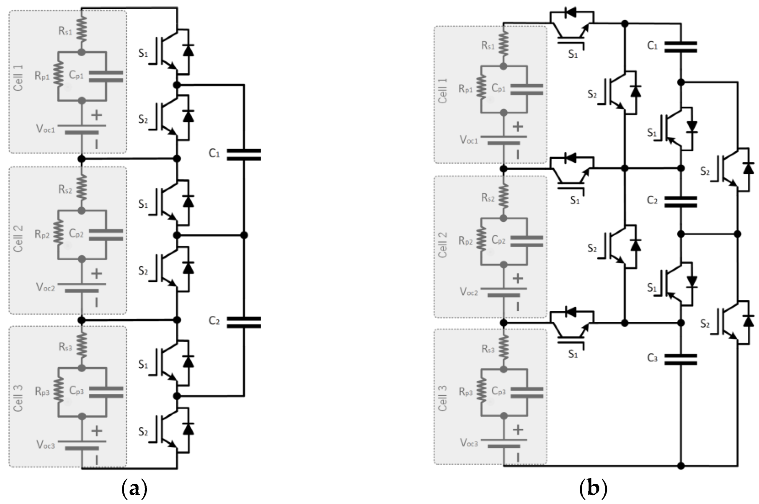
The switched-capacitor (SC) converter allows for active balancing and its main advantages are the absence of bulky magnetic components and simplicity in control since it is controlled using a fixed frequency and duty cycle. Thus, the converter can be developed with a reduced size and cost [28]. The conventional structure of the SC converter is present in Figure 2a. In this structure, the energy only flows between two adjacent cells. The balancing time is also high, which makes the structure difficult to use with a large number of cells. The authors in [29] presented a different structure, as demonstrated in Figure 2b, whose objective was to mitigate the problems of the conventional structure. Analogously to the conventional method, all the semiconductors are controlled by a pair of complementary signals with fixed frequency and duty cycle. The main advantage of this converter is the possibility of energy being transferred from the cell with the highest voltage to the cell with a lower voltage value. Thus, the balancing time becomes significantly shorter, making this converter more suitable for a larger number of cells. In addition to this reference, [28] presented a different converter, but in line with the aforementioned principle. On the other hand, all of the positive points of the capacitor-based balancing methods are applied, that is, they depend on the voltage difference between the cells, which may result in a greater imbalance due to the differences in the internal resistances of the cells [30]. Finally, another issue of the SC is that the cell voltages cannot be balanced due to the voltage drop on the controlled semiconductors.
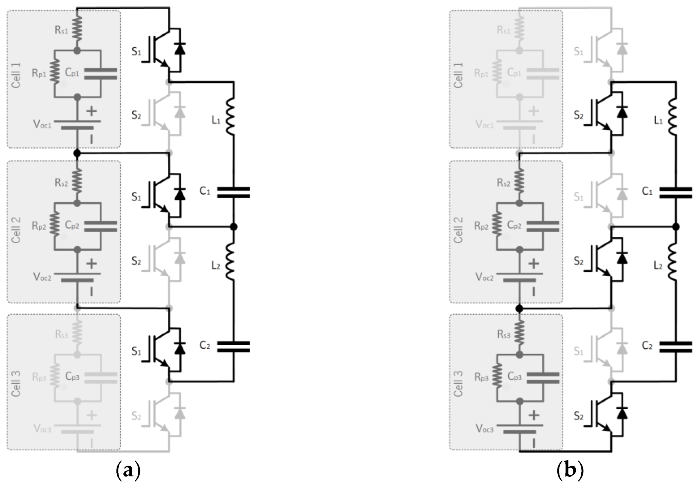
From the analysis of Figure 2b, for a battery formed by n cells in series, n capacitors, Cn, and 4n−3 controlled semiconductors, Sx, are needed, where x is the index of the controlled semiconductor. Regarding the controlled semiconductors, Sn, they are divided into two groups, S1 and S2. The control of the SC converter is carried out with the help of a pair of complementary signals with a short dead time between them in order to prevent a short circuit to the voltage source, as presented in Figure 3. It is important to note that if the capacitors are initially discharged, the duty cycle must be gradually increased to prevent excessively high currents.
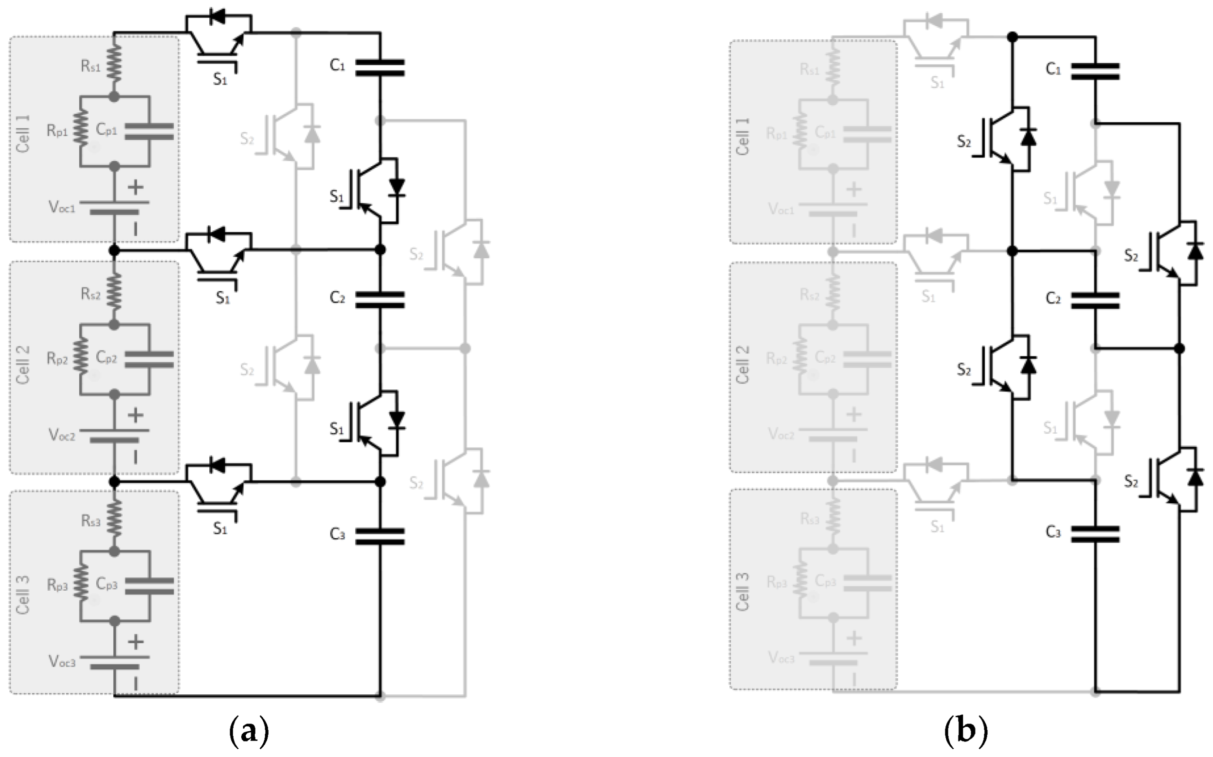
To analyze the behavior of the converter presented in Figure 2b, it is possible to divide the operation into two stages, as shown in Figure 4. The first stage, T1, begins with the semiconductor S1 closed and S2 open, as illustrated in Figure 4a. In this stage, there are two possible situations, that is, if the capacitor voltage is higher than the cell voltage, the capacitor, Cn, will charge the cell. Otherwise, the capacitor, Cn, will charge through the cell. The variations in the capacitor voltage and current during the charging process of the capacitors are expressed in the Equations (1) and (2), where VCnmin is the initial voltage of capacitor Cn. The Vcelln is the voltage of Cell n, r is the sum of the ESR of the capacitor and ON-resistance of the switches, and C is the capacitor value. In the case the capacitor has a higher voltage, Cn will discharge to the battery cell. The variations in the capacitor’s voltage and current during the discharging process are described by Equations (3) and (4), where VCnmax is the initial voltage of Cn.
V C n ( t ) = V c e l l n ( V c e l l n V C n m i n ) e t r C
i C n ( t ) = V c e l l n V C n m i n R e t r C
V C n ( t ) = V c e l l n + ( V C n m a x V c e l l n ) e t r C
i C n ( t ) = V C n m a x V c e l l n R e t r C
Regarding the second stage, T2, the semiconductor S1 opens and S2 closes, as can be seen in Figure 4b. Thus, all the capacitors, Cn, are connected in parallel and the load flows from the capacitors that have a higher voltage to those that have a lower voltage value. For Cn with the initial voltage VCnmin, it will be charged by the constant voltage Vav during T2. The variation in the capacitor’s voltage and current during the charging process can be expressed by Equations (5) and (6). Similarly, for Cn with the higher initial voltage, VCnmax, it will discharge to the constant voltage source Vav and the capacitor voltage and current are expressed by Equations (7) and (8) [31].
V C n ( t ) = V a v ( V a v V C n m i n ) e t r C
i C n ( t ) = V a v V C n m i n R e t r C
V C n ( t ) = V a v + ( V C n m a x V a v ) e t r C
i C n ( t ) = V C n m a x V a v R e t r C

2.2. Double-Tiered Switched-Capacitor

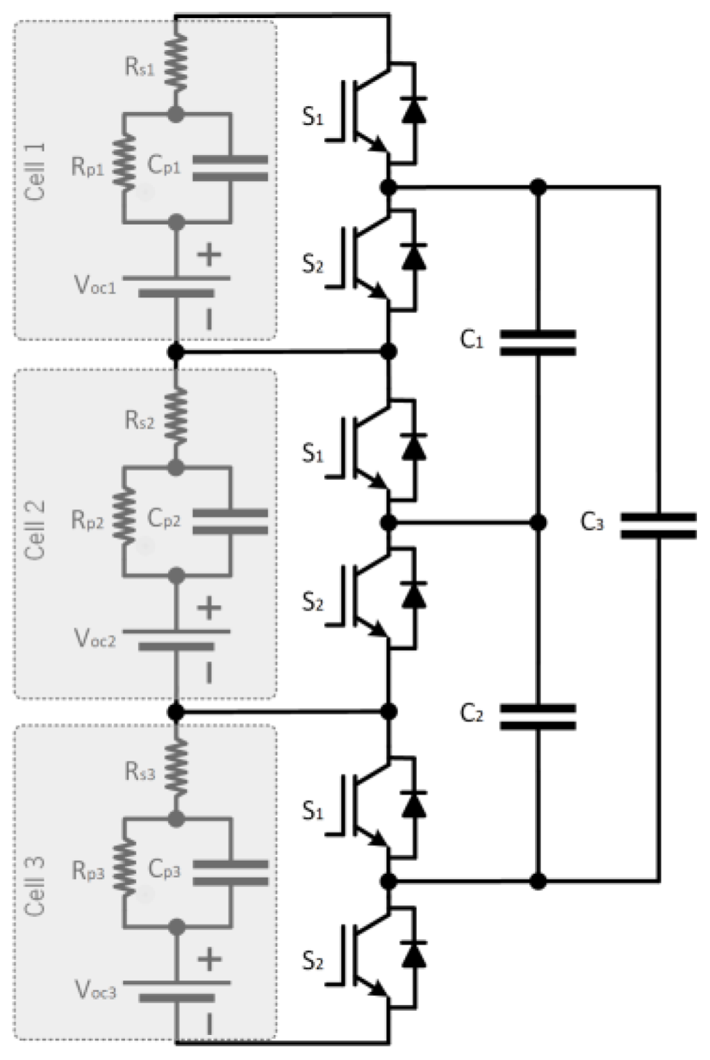
The double-tiered switched capacitor (DTSC) converter is a derivation of the SC, as shown in Figure 2a. The main difference between them is that the DTSC uses two levels of capacitors for energy reduction, as shown in Figure 5. According to what has been illustrated, for a battery formed by n cells in series, n capacitors, Cn, and 2n controlled semiconductors, Sx, are needed, where x is the index of the controlled semiconductor. Analogously to the SC converter, the control of the DTSC converter was also carried out with the help of a pair of complementary fixed frequency and duty cycle signals [32]. Having more layers means more paths between the cells, and consequently, less impedance in the transport of the charge over a specific distance. With this improvement, the cells that are not directly connected through the capacitor of the first level now have the opportunity to exchange energy through the capacitors of the second level. As a result, the balancing time of the DTSC can be significantly reduced without major hardware or control modifications [33]. On the other hand, although the balancing time is even shorter, there is still no possibility of a direct energy exchange between all cells. In addition, the same disadvantages related to the capacitor of the SC converter also apply to this converter [30].
To analyze the behavior of the converter, it is possible to divide the operation into two stages (Figure 6). The first stage, T1, begins with the semiconductor S1 being closed and S2 open, as illustrated in Figure 6a. In this stage, only cells 1 and 2 can exchange energy. Thus, two cases are possible, that is, if the capacitor voltage is higher than the cell 1 or 2 voltage, the capacitor, Cn, will discharge to charge the cell. Otherwise, the capacitor, Cn, will charge through the cell. Regarding the second stage, T2, the semiconductor S1 opens and S2 closes, as can be seen in Figure 6b. In this, only cells 2 and 3 can exchange energy, with a behavior similar to the first stage [33]. The variation in the capacitor’s voltage and current during the charging process can be expressed by Equations (9) and (10), where VCnmax and VCnmin are the initial voltage and final voltage, respectively, and r is the sum of the ESR of the capacitor and the ON-resistance of the switches.
V C n ( t ) = V C n m a x V C n m i n 1 e t r C + V C n m a x
i C n ( t ) = V C n m a x V C n m i n R e t r C

2.3. Switched Capacitor–Inductor

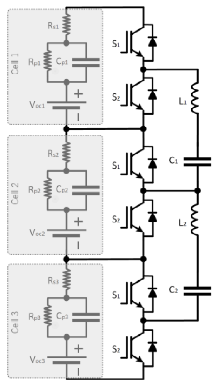
The switched capacitor–inductor (SCI) or resonant switched-capacitor converter, as represented in Figure 7, uses two energy-storing elements. This converter presents a scheme similar to the SC, but an inductor is added in series with the capacitor. The main problem of the switched capacitor topology, as above-mentioned, is that the cell voltages cannot be balanced due to the voltage drop on the controlled semiconductors [34]. Therefore, this converter emerged with the same operating principle and with zero-current switching (ZCS) to balance the cell voltage automatically. This scheme solves a disadvantage of the SC converter, since the inductive element opposes sudden changes in the current. Therefore, current peaks are avoided when switching. However, it is difficult to apply this topology to systems with a low voltage between cells. This is, if the voltage difference between the collector and the emitter is lower than the forward voltage drop, the controlled semiconductor will not conduct, resulting in a residual voltage between cells. Furthermore, the compensation current becomes smaller as the voltage difference becomes smaller, resulting in a higher balancing time. The architecture consists of n cells connected in series, 2n controlled semiconductors, Sx, n−1 capacitors, Cy, and n−1 inductors, Ly, where x and y are the index of the controlled semiconductor and capacitors and inductors, respectively [35].
To analyze the SCI behavior, it is possible to divide the operation into two stages (Figure 8). The first stage, T1, starts with the semiconductor S1 closed and S2 open, as illustrated in Figure 8a. In this stage, only cells 1 and 2 can make energy exchanges. Thus, two cases are possible, that is, if the capacitor voltage is higher than the cell 1 or 2 voltages, the capacitor Cy and inductor Ly will discharge to charge the cell. Otherwise, the capacitor Cy and inductor Ly will charge through the cell. The state equations for stage 1 are present in Equations (11) and (12), and the equations that characterize the voltage across the capacitor and the resonant current are Equations (13) and (14). ∆Vy is the amplitude of VCy and Im is the amplitude of the resonant current ir. ω is the resonant angular frequency and is equal to 1 / L y C y , and φ is the initial angle of the resonant state.
i r ( t ) = C y d V C y d t
L n d i r d t + V C y = V c e l l n
V C y ( t ) = V c e l l n + V y cos ( ω t + φ )
i r ( t ) = I m sin ( ω t + φ )
Regarding the second stage, T2, the semiconductor S1 opens and S2 closes, as can be seen in Figure 8b. In this stage, only cells 2 and 3 can make energy exchanges, with the behavior being similar to the first stage [34]. The equations that characterize the voltage across the capacitor and the resonant current are shown as (15) and (16).
V C n ( t ) = V c e l l n V n cos ( ω t + φ )
i r ( t ) = I m sin ( ω t + φ )
To change the operation state of the power semiconductor when the current passes through zero, Equation (17) determines the system’s frequency, f, where R is the circuit’s resistance (includes the internal resistance of the power semiconductor, inductor, and capacitor), L is the value of the inductor’s inductance, and C is the value of the capacitor’s capacity.
f = 1 2 π 4 L R 2 C 4 L 2 C

2.4. Single Inductor

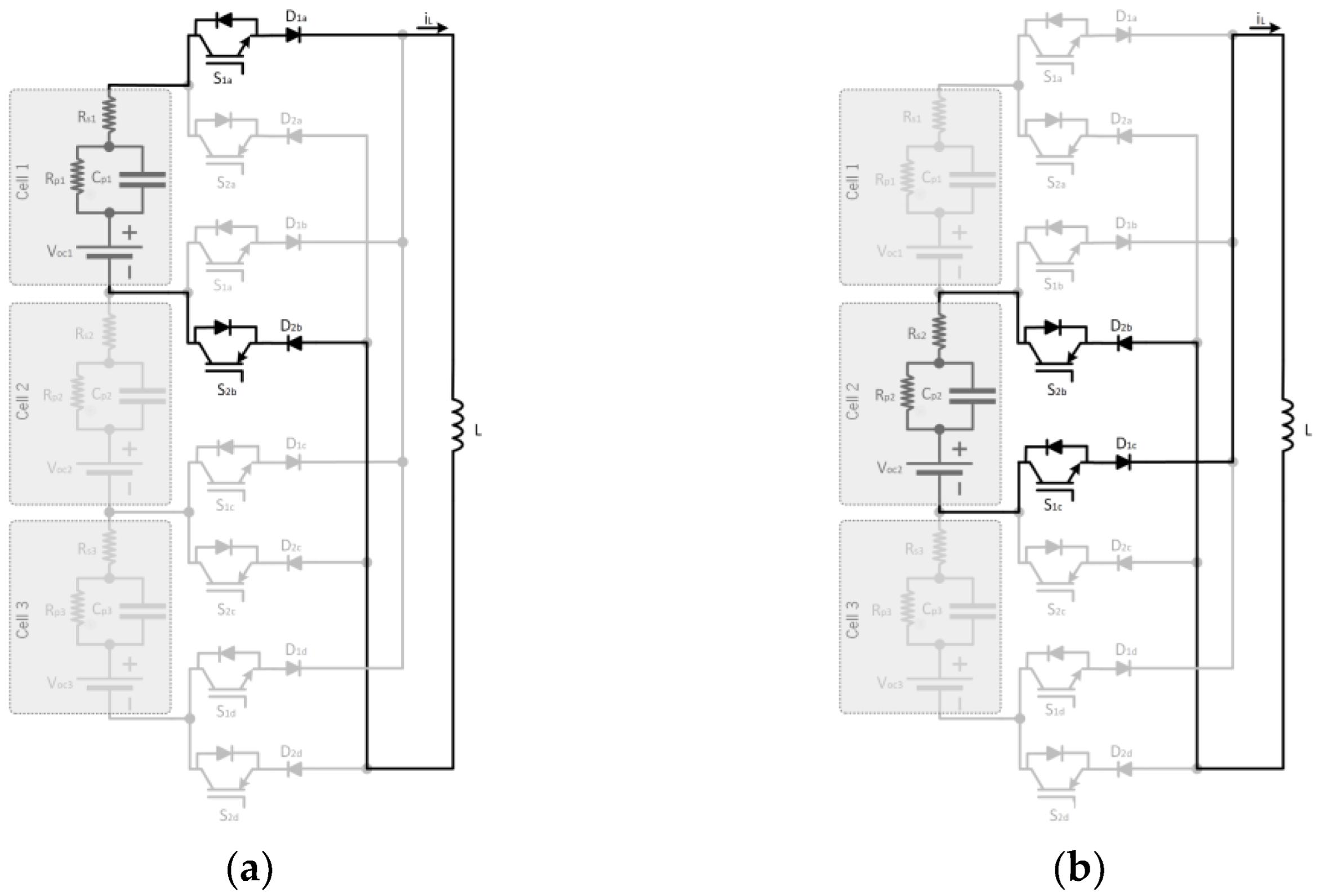
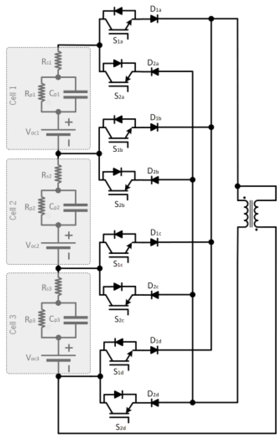
The single inductor (SI) converter belongs to the family of converters whose balance is carried out using inductive elements. In this case, only one inductor is used for balancing. Thus, the positive terminals of each cell are connected to one inductor terminal, while the cells’ negative terminals are connected to the other inductor terminal. In addition, as illustrated in Figure 9, for a battery formed by n cells in series, 2n + 2 controlled semiconductors, Sxy, and 2n + 2 diodes, Dxy, are necessary, where x represents the conduction orientation and considering the image can be 1 or 2. and y identifies the number of arms and considering the image can be a, b, c, or d. This converter presents advantages such as high efficiency in balancing, a modular design, and the possibility of transferring energy not only between adjacent cells but between all of them. The main disadvantage is related to the balancing process since the energy is only transferred to the cell with the lowest voltage in the second part of the period [36]. In addition, it requires more hardware, specifically diodes, PWM channels, and voltage sensors.
To analyze the SI behavior, it is possible to divide the operation into two stages, as illustrated in Figure 10. For example, it was assumed that cell 1 has a higher voltage than cell 2, and therefore, cell 1 will have to discharge while cell 2 has to charge. To allow cell 1 to discharge, in the first stage, T1, the semiconductors S1a and S2b close, and all the others remain open, as illustrated in Figure 10a. The current flowing through the inductor iL and the energy transferred by the cell can be calculated using Equations (18) and (19), respectively, where T is the period, D is the duty cycle, and Vcell is the cell voltage. Regarding the second stage, T2, cell 2 will charge, since the semiconductors S2b and S1c close and all the others remain open, as illustrated in Figure 10b. The current flowing through the inductor decreases with a constant slope and can be calculated using Equation (20). Regarding the energy transferred, as there is only an exchange between two cells, the equation for calculating is the same (Equation (19)) [37].
i L ( t ) = V c e l l 1 L t
E = 1 2 i L D T
i L ( t ) = V c e l l 1 L D T V c e l l 2 L t
Table 1 summarizes the actions of the controlled semiconductors considering the voltage of each cell and comparing them with the others. The value of inductance, L, can be calculated using Equation (21).
L V c e l l D 2 T 2 n 1 i L

2.5. Switched Inductor

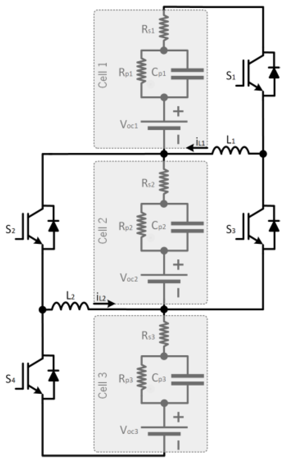
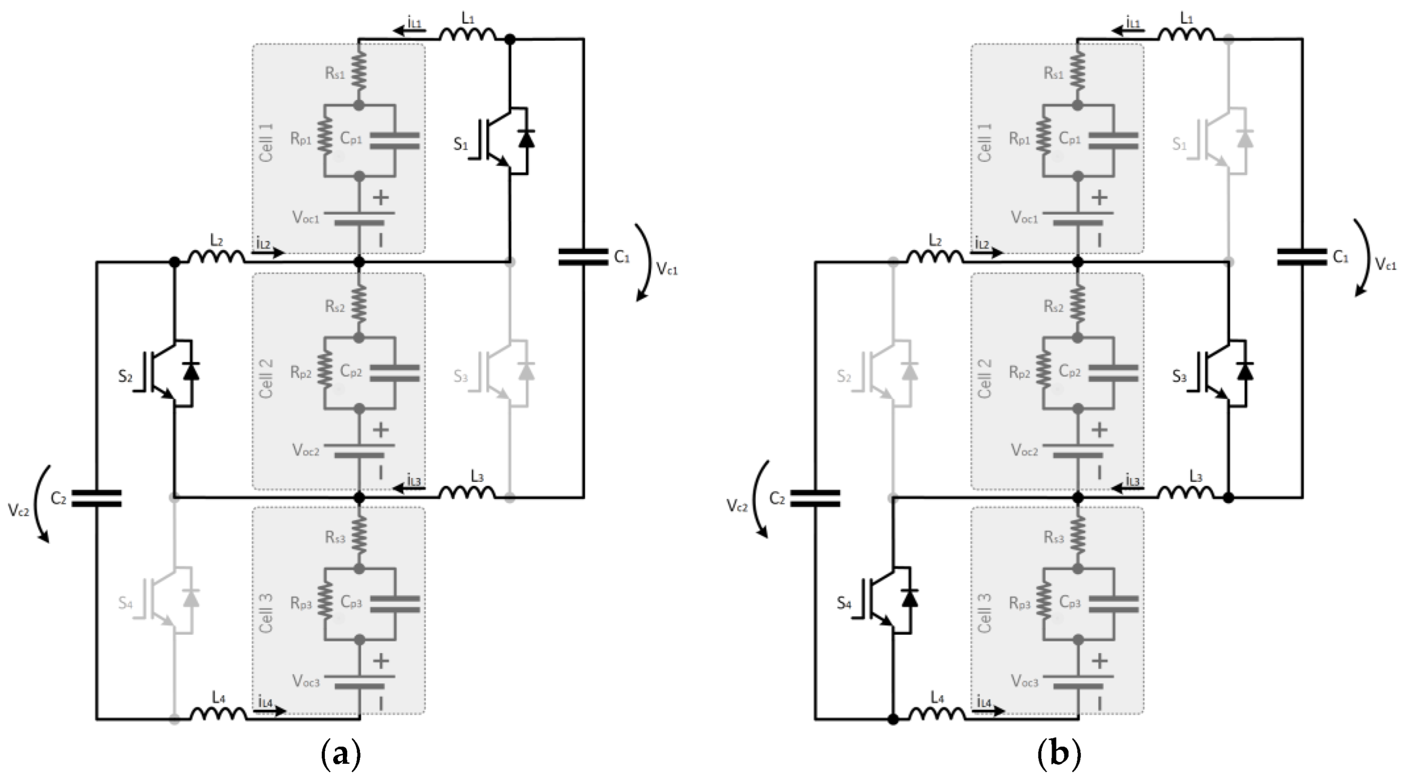
The switched inductor (SwI) converter, also often referred to as a buck-boost converter, belongs to the family of converters whose balance is carried out using inductive elements. In the converter present in Figure 11, an inductor was connected between two adjacent cells, allowing for the exchange of energy between the cell with a higher voltage value and the cell with a lower voltage value. It requires 2(n − 1) controlled semiconductors, Sx, and n − 1 inductors, Ly, where x and y are the index of the controlled semiconductor and inductors, respectively, to balance the n cells [38]. The advantage of this converter is the high balancing current, thus allowing for faster balancing, greater efficiency than the capacitor-based topology, and lower production cost than the transformer-based topologies. On the other hand, this balancing circuit has a higher cost than the capacitor-based topology and a slower balancing than the transformer-based topologies. In addition, a filter capacitor may be required due to the high switching frequency [39].
The principle of the SwI converter operation can be divided into two phases. In order to analyze the converter, three cells were considered. Thus, there were four controlled semiconductors, S1, S2, S3 and S4 (S1 and S2 are complementary to S3 and S4, respectively), two inductors L1 and L2, and the current in each inductor iL1 and iL2. In the first phase, the controlled semiconductors S1 and S2 close in order to allow the cells with a higher voltage to transfer energy to the inductors, while the controlled semiconductors S3 and S4 remain open, as can be seen in Figure 12a.
In the second phase, the controlled semiconductors S1 and S2 open, while the controlled semiconductors S3 and S4 will close, allowing the stored energy to flow from the inductors to the adjacent cells, as represented in Figure 12b.
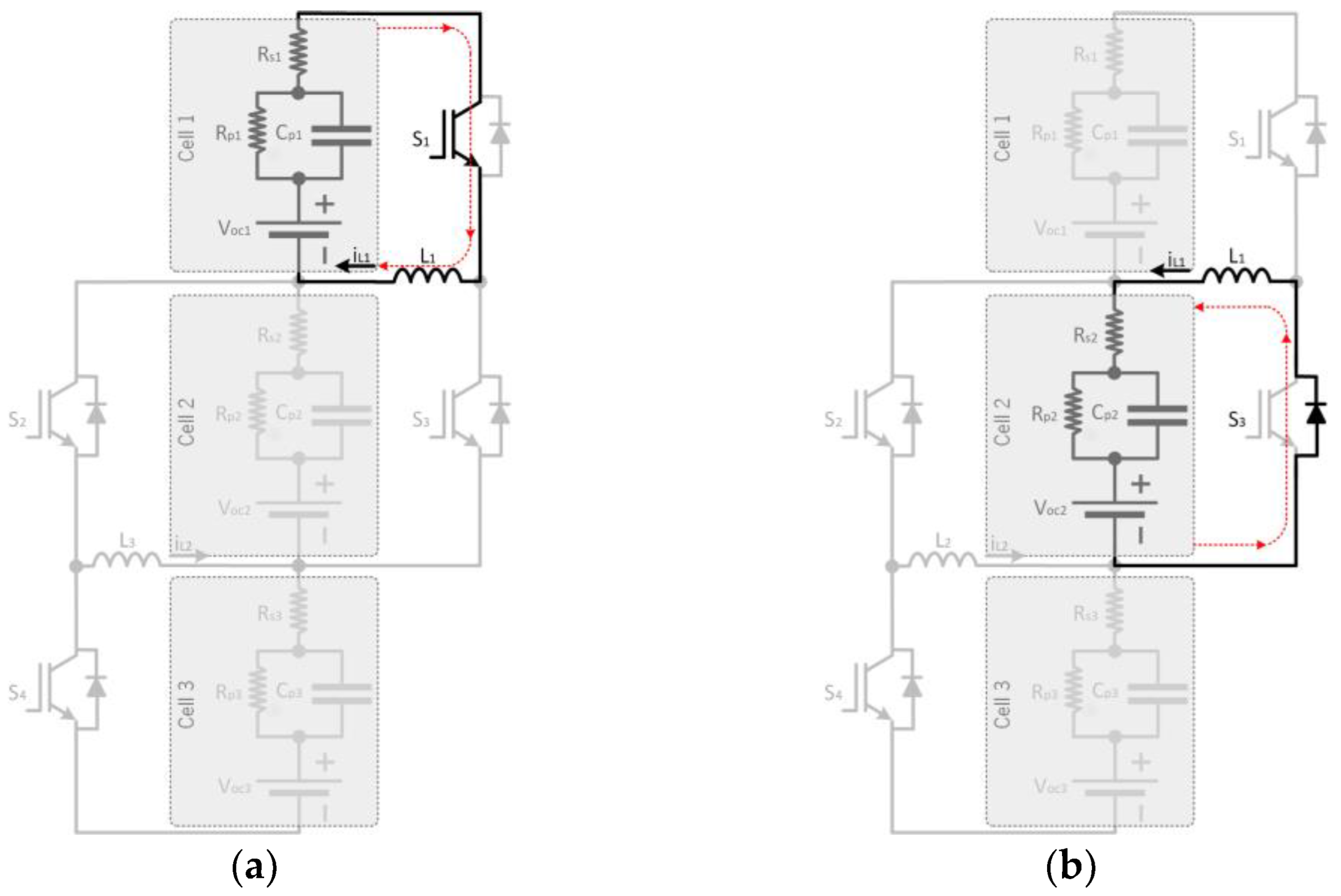
If the voltage of cell 1 is higher than the voltage of cell 2, the controlled semiconductor S1 closes while the controlled semiconductor S3 remains open, as can be seen in Figure 13a. The current flowing through L1 can be calculated through Equation (22).
i L 1 ( t ) = V c e l l 1 L 1 t
Thus, when the controlled semiconductor S1 opens, the current flows through the antiparallel diode of the controlled semiconductor S3 to charge cell 2, as represented in Figure 13b [23]. The current flowing through L1 can be calculated through Equation (23).
i L 1 ( t ) = V c e l l 1 L 1 D T V c e l l 2 L 1 t

2.6. Cuk

The Cuk type power converters can be applied in the balancing of cells in a battery. The main advantage of balance using Cuk converters is the control of the input current and the current delivered to each cell. In this way, none of the cells presents a pulsating current. However, they are expensive because they have more components, and the design can be complex [23].
Cuk is a non-isolated dc–dc converter, whose main characteristic is to present an inverse voltage at the output. The conventional circuit of the Cuk converter is represented in Figure 14. The Cuk converter presents a bidirectional energy transfer capacity with high efficiency. This requires 2(n − 1) controlled semiconductors and inductors and n − 1 capacitors to balance n cells. The presence of inductive elements at the input and the output stage allows for the regulation of the current in the cells involved in the energy transfer. However, since a converter is required for each pair of adjacent cells, it becomes an implementation with a high cost. The control is very similar to the switched inductor topology. This converter can be analyzed as a cascaded buck-boost converter and the operating principle is divided into two stages [23].
To analyze the SI behavior, it is possible to divide the operation into two stages, as illustrated in Figure 15. Initially, the controlled semiconductors S1 and S2 are turned on, while the others remain open, as shown in Figure 15a. In the next stage, the controlled semiconductors S3 and S4 close, while the others remain open (Figure 15b) [40]. The operating principle was simplified for three cells to investigate the circuit.
In the first mode, S1 is closed and S2 is open, as can be seen in Figure 16a. The equations that allow us to calculate the voltage in each cell are shown as (24) and (25):
V c e l l 1 ( t ) = L 1 d i L 1 d t
V c e l l 2 ( t ) = L 2 d i L 2 d t + V C 1
In the next mode, S1 is open and the diode in anti-parallel to the controlled semiconductor S2 conducts, as represented in Figure 16b. The equations that allow for the calculation of the voltage in each cell are shown as (26) and (27):
V c e l l 1 ( t ) = L 1 d i L 1 d t + V C 1
V c e l l 2 ( t ) = L 2 d i L 2 d t
The expression for the average current in the inductor can be obtained from the load balancing of capacitor C1 is Equation (28), where D is the duty cycle and T is the period [41].
i L 1 1 D T i L 2 D T = 0

2.7. Single Flyback

The single flyback (SF) converter, which is represented in Figure 17, uses a transformer to balance the cells. The single transformer balancing method shares the same topology as the SI. Thus, as illustrated in Figure 17, for a battery formed by n series cells, 2n + 2 controlled semiconductors, Sxy, and 2n + 2 diodes, Dxy, are required, where x represents the conduction orientation and considering the image can be 1 or 2, and y identifies the number of arms and considering the image can be a, b, c, or d. This converter allows for faster balancing than the capacitor and inductor-based topologies. On the other hand, it has a higher cost and lower efficiency [39].
In order to study the behavior of the converter, it was possible to divide the operation into two stages (Figure 18). As an example, it was assumed that cell 1 had a higher voltage than cell 2, and, therefore cell 1 will have to discharge and cell 2 will have to charge. In order to allow the cell to discharge, in the first stage, T1, the semiconductors S1a and S2b close, and all the others remain open, as illustrated in Figure 18a. Thus, the current in the transformer increases to the upper limit, according to Equation (29), meaning that energy is transferred from cell 1 to the transformer. Lm is the magnetizing inductance and iLm is the magnetizing current.
i L m t = V c e l l L m ( t T 1 )
Regarding the second stage, T2, cell 2 will charge, since the semiconductors S2b and S2c close and all the others remain open, allowing the energy stored in the transformer to charge the cells, as illustrated in Figure 18b. The Dxy diodes are used to protect the cells from possible short circuits [42]. It is possible to calculate the current ipack using Equation (30), where k is the turn’s ratio of the secondary winding of the transformer and ipk is the maximum value of the iLm. Table 1, as for the single inductor converter, summarizes the actions of the controlled semiconductors considering the voltage of each cell and comparing it with the others [43].
i p a c k t = 1 n ( i p k V p a c k n L m t T 2 )

2.8. Multi-Winding Transformer

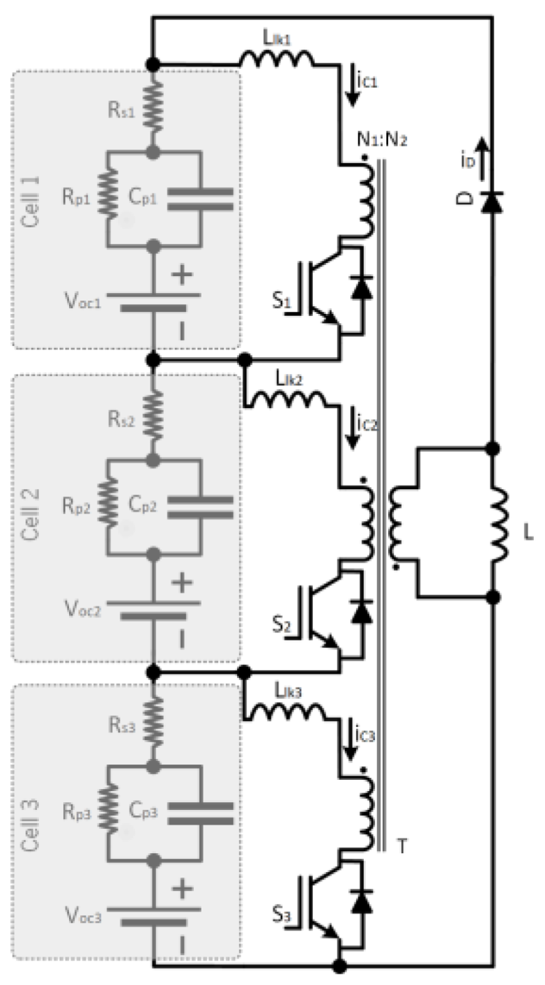
The multi-winding transformer (MWT) based balancing method, represented in Figure 19, has advantages such as fast balancing and simple control techniques. On the other hand, the circuit presents complexity in the design of the MWT and has a limited number of windings due to the correspondence of the parameters for the turn’s ratio and leakage inductance, especially for a large number of cells [44]. The circuit consists of n cells connected in series. Each cell is associated with a primary winding of transformer T and a controlled semiconductor Sn. The diode on the secondary side allows for discharging the magnetization inductance of the secondary. The MWT converter balances by switching the controlled semiconductor Sn with a constant frequency and duty cycle [45].
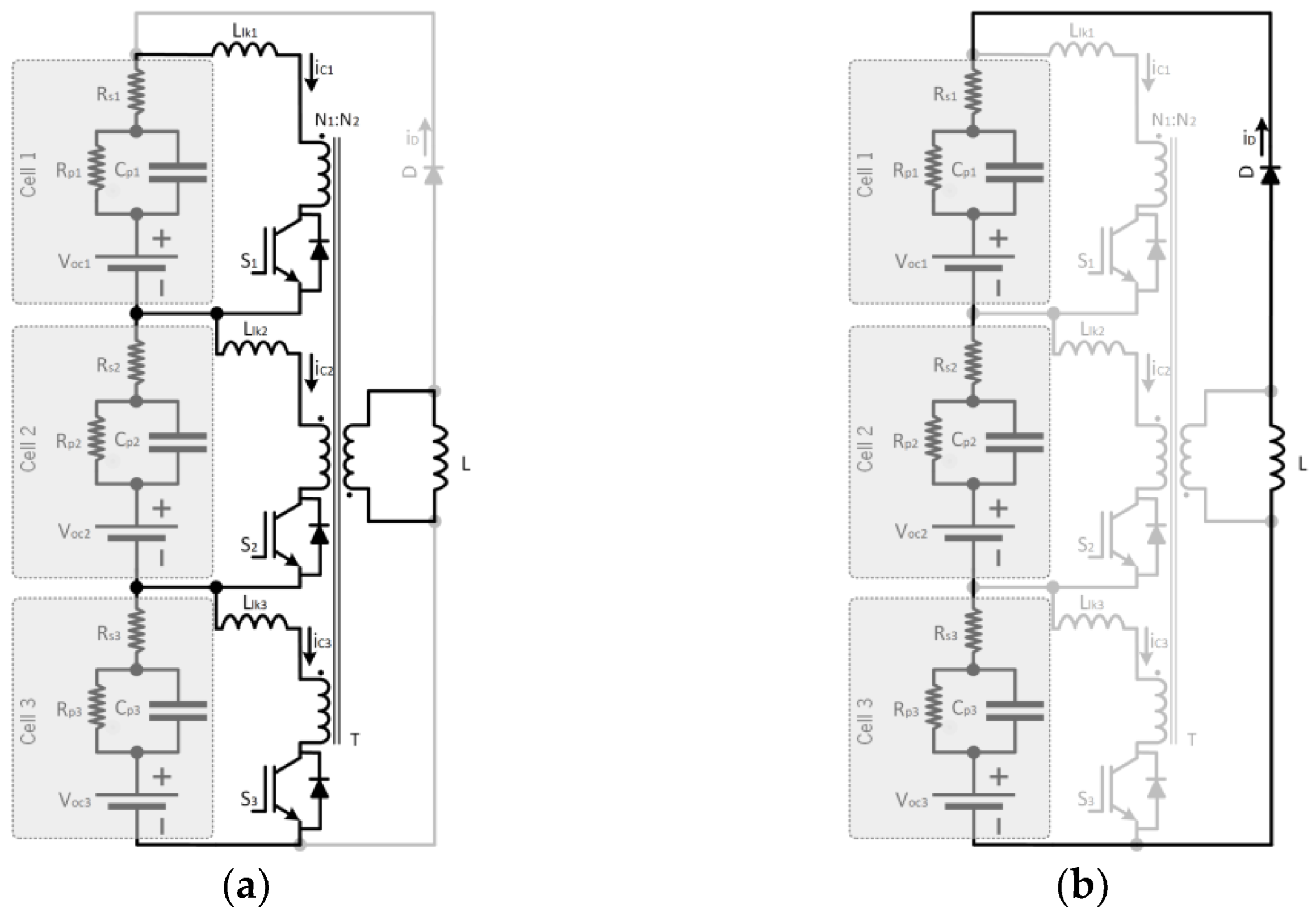
The operation of the MWT converter can be divided into two stages, as shown in Figure 20. In Stage 1, all three controlled semiconductors (S1, S2, and S3) are closed simultaneously, as seen in Figure 20a. During this stage, energy is transferred from the cells with higher voltage to the cells with lower voltage through transformer T. The voltage across L can be calculated through Equation (31).
Assuming a higher voltage in cells 2 and 3, and a lower voltage in cell 1, the currents ic2 and ic3 flow from the cells to the transformer, while the current ic1 flows from the transformer to the cell. The voltage and current across L can be calculated through Equations (31) and (32), respectively.
V L ( t ) = L d i L d t
i L = i c 1 + i c 2 + i c 3
In Stage 2, two modes of operation are possible. Initially, S1, S2, and S3 are open simultaneously, as seen in Figure 20b. This causes the voltage on inductor L to become negative and the current to flow through the diode, discharging L. When the current iD reaches zero, the converter enters the second mode of operation, known as discontinuous conduction mode (DCM) [46]. The voltage across L can be calculated using Equation (33).
V L = ( V c e l l 1 + V c e l l 2 + V c e l l 3 )

3. Discussion

This section compares the converters presented and described above in terms of components and performance. This comparative analysis took into consideration a BMS consisting of three cells. Thus, if BMS for a larger number of cells is required, an interpolation would be necessary and the method presented here can be used to identify the best solution.
The first comparison was based on the number of capacitors, inductors, diodes, MOSFET, and transformers in a three-cell converter. The comparison is shown in Figure 21. As can be seen, the SC used the higher number of MOSFETs (nine in total). This converter also requires more capacitors (three in total), as does the SCI converter (also three in total). Regarding the use of diodes, both the SI and SF converters used eight diodes. In terms of the use of inductors, it was the Cuk converter that had the most (four in total). Regarding the transformers, only the SF and MWT topologies used one, but the first one only used one primary and one secondary, while the second one used as many primaries as the number of cells. Considering the sum of all variants (capacitors, inductors, diodes, MOSFETs, and transformers), the SI and SF topologies required the most elements (17 in total), and the MWT converter required the least (six in total).
In addition to the constitution, which will have a direct impact on the cost, size, and weight of the BMS, the performance must also be considered. The efficiency is a critical aspect when it comes to active cell equalization circuits. The efficiency of these circuits plays a significant role in determining the overall performance of the energy storage and management system of EVs. By incorporating features such as low resistance components, high switching frequencies, and advanced control techniques, the efficiency of these circuits can be improved, which leads to improved battery performance, extended battery life, and enhanced range in EVs. In order to implement a metric about the circuit balancing efficiency, the comparison of active and passive balancing strategies is demonstrated in Figure 22. Figure 22a shows the cells’ initial SoC, a significant unbalance being visible. Figure 22b shows the cells’ SoC after an ideal passive balancing, with all the cells keeping the same SoC equal to the lowest cells’ SoC before balancing. Finally, Figure 22c shows the cells’ SoC after an ideal active balancing with all the cells presenting the same SoC, equal to the average SoC of the cells before balancing. In this theoretical scenario, all of the reusable energy ( E r e u s a b l e ) was redistributed by the cells ( E r e u s e d ) without losses, corresponding to a 100% efficiency calculated by Equation (34). In practice, the converters used to balance the cells presented some losses, so the efficiency will always be less than 100%. The worst scenario corresponded to the passive balancing where all the energy was dissipated ( E r e u s e d = 0 ) , corresponding to 0% efficiency.
η = E r e u s e d E r e u s a b l e × 100
Table 2 presents a comparative analysis of the efficiency of some active balancing converter efficiencies found in the literature. As it is possible to see, various converter topologies presented an efficiency greater than 90%, with the best performance of 99.7% being achieved with the 14 cell SwI topology.

4. Conclusions

In this paper, the concept of active cell equalization was investigated. Active cell equalization circuits are an important aspect of the design and operation of a BMS for electric vehicles. These circuits serve to regulate the SoC of each cell within the battery pack to ensure its longevity and prevent harmful situations. Through the transfer of energy from cells with high charge to cells with low charge, the active equalization method helps to keep the battery pack operating at peak performance and increases its overall efficiency. This makes active cell equalization circuits an essential component in electric vehicles, and as the popularity of EVs continues to grow, it is likely that the importance of this technology will also continue to grow.
All the presented and discussed converter topologies have their own advantages and disadvantages and can be applied to different scenarios depending on the specific requirements. A study on the performance of active balancing converters revealed various topologies with an energy efficiency higher than 90%, very promising data that support that the active balancing of cells can represent significant energy savings, which is why the study and development of these solutions is of great importance.

Author Contributions

Conceptualization, J.P.D.M. Formal analysis, J.P.D.M.; Investigation, J.P.D.M., J.G.P. and L.A.M.B.; Methodology, J.P.D.M., J.G.P. and L.A.M.B.; Supervision, J.G.P. and L.A.M.B.; Validation, J.P.D.M., J.G.P. and L.A.M.B.; Writing—original draft, J.P.D.M.; Writing—review & editing, J.P.D.M., J.G.P. and L.A.M.B.. All authors have read and agreed to the published version of the manuscript.

Funding

This work was supported by FCT—Fundação para a Ciência e Tecnologia, within the R&D Units Project Scope UIDB/00319/2020. Luis A. M. Barros is supported by the doctoral scholarship PD/BD/143006/2018, granted by the Portuguese FCT foundation.

Data Availability Statement

Not applicable.

Conflicts of Interest

The authors declare no conflict of interest.

References

  1. Silva, C.M.; Santo, B.E.; Ferreira, L.T. The integration of E-Mobility in smart cities: The Portuguese scenario for EV charging in street light circuits. Inst. Eng. Technol. (IET) 2022, 2022, 472–475. [Google Scholar]
  2. Ahmed, A.A.; Nazzal, M.A.; Darras, B.M.; Deiab, I.M. Global warming potential, water footprint, and energy demand of shared autonomous electric vehicles incorporating circular economy practices. Sustain. Prod Consum. 2023, 36, 449–462. [Google Scholar] [CrossRef]
  3. Monteiro, V.; Gonçalves, H.; Afonso, J.L. Impact of Electric Vehicles on Power Quality in a Smart Grid Context. In Proceedings of the 11th International Conference on Electrical Power Quality and Utilisation, Lisbon, Portugal, 17–19 October 2011; pp. 1–6. [Google Scholar]
  4. Greenhouse Gas Emissions from Energy Data Explorer–Data Tools-IEA. Available online: https://www.iea.org/data-and-statistics/data-tools/greenhouse-gas-emissions-from-energy-data-explorer (accessed on 9 February 2023).
  5. Silva, Ó.; Cordera, R.; González-González, E.; Nogués, S. Environmental impacts of autonomous vehicles: A review of the scientific literature. Sci. Total Environ. 2022, 830, 154615. [Google Scholar] [CrossRef] [PubMed]
  6. Barzkar, A.; Ghassemi, M. Electric power systems in more and all electric aircraft: A review. IEEE Access 2020, 8, 169314–169332. [Google Scholar] [CrossRef]
  7. Sumsurooah, S.; He, Y.; Torchio, M.; Kouramas, K.; Guida, B.; Cuomo, F.; Atkin, J.; Bozhko, S.; Renzetti, A.; Russo, A.; et al. ENIGMA—A Centralised Supervisory Controller for Enhanced Onboard Electrical Energy Management with Model in the Loop Demonstration. Energies 2021, 14, 5518. [Google Scholar] [CrossRef]
  8. Andrea, D. Battery Management Systems for Large Lithium-Ion Battery Packs; Artech House Publishers: London, UK, 2010. [Google Scholar]
  9. Rashid, M.H. Power Electronics Handbook; Elsevier: Amsterdam, The Netherlands, 2011; pp. 225–250. [Google Scholar]
  10. Suratgar, A.A.; Menhaj, M.B. Distributed Optimization and Its Application in Electricity Grids, Including Electrical Vehicles. In Electric Transportation Systems in Smart Power Grids; CRC Press: Boca Raton, FL, USA, 2022; pp. 493–520. [Google Scholar]
  11. Williamson, S.S.; Rathore, A.K.; Musavi, F. Industrial Electronics for Electric Transportation: Current State-of-the-Art and Future Challenges. IEEE Trans. Ind. Electron. 2015, 62, 3021–3032. [Google Scholar] [CrossRef]
  12. Tan, D. Transportation Electrification: Challenges and opportunities. IEEE Power Electron. Mag. 2016, 3, 50–52. [Google Scholar] [CrossRef]
  13. Nur Halimah, P.; Rahardian, S.; Budiman, B.A. Battery Cells for Electric Vehicles. Int. J. Sustain. Transp. Technol. 2019, 2, 54–57. [Google Scholar] [CrossRef] [Green Version]
  14. Iclodean, C.; Varga, B.; Burnete, N.; Cimerdean, D.; Jurchiş, B. Comparison of Different Battery Types for Electric Vehicles. IOP Conf. Ser. Mater. Sci. Eng. 2017, 252. [Google Scholar] [CrossRef] [Green Version]
  15. Rezvanizaniani, S.M.; Liu, Z.; Chen, Y.; Lee, J. Review and recent advances in battery health monitoring and prognostics technologies for electric vehicle (EV) safety and mobility. J. Power Sources 2014, 256, 110–124. [Google Scholar] [CrossRef]
  16. Lim, K.C. Battery Management System for Electric Vehicles. Master Thesis, University of Wollongong, Hong Kong, 2017. [Google Scholar]
  17. dos Santos, B.M.B.; Manuel Rodrigues Rocha, R.; Simões Piedade, M. Battery Management System applied to Projecto FST’s EV prototype. Master’s Thesis, Instituto Superior Técnico, Lisboa, Portugal, 2014. [Google Scholar]
  18. Mauri Rodríguez, E. Disseny, fabricació y validació de la bateria d’alt voltatge del model de formula student CAT13. Bachelor’s Thesis, Universitat Politècnica de Catalunya, Barcelona, Spain, 2021. [Google Scholar]
  19. Jiang, B. Active Cell Balancing Algorithms in Lithium-ion Battery. Master’s Thesis, Chalmers University of Technology, Gothenburg, Sweden, 2020. [Google Scholar]
  20. Kassim, M.R.M.; Jamil, W.A.W.; Sabri, R.M. State-of-Charge (SOC) and State-of-Health (SOH) Estimation Methods in Battery Management Systems for Electric Vehicles. In Proceedings of the 2021 IEEE International Conference on Computing, ICOCO 2021, Kuala Lumpur, Malaysia, 17–19 November 2021; Institute of Electrical and Electronics Engineers Inc.: Piscataway, NJ, USA, 2021; pp. 91–96. [Google Scholar]
  21. Lee, C.Y.; Lee, S.J.; Tang, M.S.; Chen, P.C. In Situ Monitoring of Temperature inside Lithium-Ion Batteries by Flexible Micro Temperature Sensors. Sensors 2011, 11, 9942–9950. [Google Scholar] [CrossRef]
  22. Tessier, A.O.; Dubois, M.R.; Trovão, J.P. Real-Time Estimator Li-ion Cells Internal Resistance for Electric Vehicle Application. World Electr. Veh. J. 2016, 8, 410–421. [Google Scholar] [CrossRef] [Green Version]
  23. Alvarez-Diazcomas, A.; Estévez-Bén, A.A.; Rodríguez-Reséndiz, J.; Martínez-Prado, M.A.; Carrillo-Serrano, R.V.; Thenozhi, S. A review of battery equalizer circuits for electric vehicle applications. Energies 2020, 13, 5688. [Google Scholar] [CrossRef]
  24. Omariba, Z.B.; Zhang, L.; Sun, D. Review of Battery Cell Balancing Methodologies for Optimizing Battery Pack Performance in Electric Vehicles. IEEE Access 2019, 7, 129335–129352. [Google Scholar] [CrossRef]
  25. Kıvrak, S.; Özer, T.; Oğuz, Y.; Kelek, M.M. Novel active and passive balancing method-based battery management system design and implementation. J. Power Electron. 2021, 21, 1855–1865. [Google Scholar] [CrossRef]
  26. Aminudin, I.R.; Aritonang, S. Comparison of Active and Passive Balancing Methods of Li-Ion Battery Management Systems in Vehicles and Communication Devices for Supporting Defense Systems in IKN. UIJRT United Int. J. Res. Technol. 2022, 3, 98–105. [Google Scholar]
  27. Gabbar, H.; Othman, A.; Abdussami, M. Review of Battery Management Systems (BMS) Development and Industrial Standards. Technologies 2021, 9, 28. [Google Scholar] [CrossRef]
  28. Ye, Y.; Cheng, K.W.E. Modeling and Analysis of Series-Parallel Switched-Capacitor Voltage Equalizer for Battery/Supercapacitor Strings. IEEE J. Emerg. Sel. Top. Power Electron. 2015, 3, 977–983. [Google Scholar] [CrossRef]
  29. Ye, Y.; Cheng, K.W.E. An Automatic Switched-Capacitor Cell Balancing Circuit for Series-Connected Battery Strings. Energies 2016, 9, 138. [Google Scholar] [CrossRef] [Green Version]
  30. Yildirim, B.; Elgendy, M.; Smith, A.; Pickert, V. Evaluation and Comparison of Battery Cell Balancing Methods. In Proceedings of the 2019 IEEE PES Innovative Smart Grid Technologies Europe (ISGT-Europe), Bucharest, Romania, 29 September–2 October 2019; pp. 1–5. [Google Scholar]
  31. Sailaja, D.; Kiran, P.P.; Reddy, K. Modeling and Analysis of Series Parallel Switched-Capacitor Voltage Equalizer for Battery/Supercapacitor Strings; The Hong Kong Polytechnic University Department of Electrical Engineering: Hong Kong, 2016. [Google Scholar]
  32. Daowd, M.; Antoine, M.; Omar, N.; den Bossche, P.; van Mierlo, J. Single Switched Capacitor Battery Balancing System Enhancements. Energies 2013, 6, 2149–2174. [Google Scholar] [CrossRef] [Green Version]
  33. Baughman, A.C.; Ferdowsi, M. Double-tiered switched-capacitor battery charge equalization technique. IEEE Trans. Ind. Electron. 2008, 55, 2277–2285. [Google Scholar] [CrossRef]
  34. Yuanmao, Y.; Cheng, K.W.E.; Yeung, Y.P.B. Zero-current switching switched-capacitor zero-voltage-gap automatic equalization system for series battery string. IEEE Trans. Power Electron. 2012, 27, 3234–3242. [Google Scholar] [CrossRef]
  35. Shang, Y.; Zhang, Q.; Cui, N.; Zhang, C.; Editors, A.; Xiong, R.; Li, H.; Zhou, J. A Cell-to-Cell Equalizer Based on Three-Resonant-State Switched-Capacitor Converters for Series-Connected Battery Strings. Energies 2017, 10, 206. [Google Scholar] [CrossRef]
  36. Reynaud, J.F.; Carrejo, C.E.; Gantet, O.; Aloïsi, P.; Estibals, B.; Alonso, C. Active balancing circuit for advanced lithium-ion batteries used in photovoltaic application. Renew Energy Power Qual. J. 2010, 1423–1428. [Google Scholar] [CrossRef]
  37. Park, S.H.; Kim, T.S.; Park, J.S.; Moon, G.W.; Yoon, M.J. A new battery equalizer based on buck-boost topology. In Proceedings of the 7th Internatonal Conference on Power Electronics, Daegu, Republic of Korea, 22–26 October 2007; pp. 962–965. [Google Scholar]
  38. Moghaddam, A.F.; van den Bossche, A. An Efficient Equalizing Method for Lithium-Ion Batteries Based on Coupled Inductor Balancing. Electronics 2019, 8, 136. [Google Scholar] [CrossRef] [Green Version]
  39. Sugumar S, H. Overview of cell balancing methods for Li-ion battery technology. Energy Storage 2021, 203, 3. [Google Scholar]
  40. Moghaddam, A.F.; van den Bossche, A. A Battery Equalization Technique Based on Ćuk Converter Balancing for Lithium Ion Batteries. In Proceedings of the 2019 8th International Conference on Modern Circuits and Systems Technologies, MOCAST 2019, Thessaloniki, Greece, 13–15 May 2019. [Google Scholar]
  41. Moghaddam, A.F.; van den Bossche, A. A ćuk converter cell balancing technique by using coupled inductors for lithium-based batteries. Energies 2019, 12, 2881. [Google Scholar] [CrossRef] [Green Version]
  42. Shin, J.W.; Seo, G.S.; Chun, C.Y.; Cho, B.H. Selective Flyback balancing circuit with improved balancing speed for series connected Lithium-ion batteries. In Proceedings of the 2010 International Power Electronics Conference-ECCE Asia-, IPEC 2010, Sapporo, Japan, 21–24 June 2010; pp. 1180–1184. [Google Scholar]
  43. Cui, X.; Shen, W.; Zhang, Y.; Hu, C. A novel active online state of charge based balancing approach for Lithium-ion battery packs during fast charging process in electric vehicles. Energies 2017, 10, 1766. [Google Scholar] [CrossRef] [Green Version]
  44. Minh Bui, T.; Kim, C.-H.; Kim, K.-H.; Bong Rhee, S. A Modular Cell Balancer Based on Multi-Winding Transformer and Switched-Capacitor Circuits for a Series-Connected Battery String in Electric Vehicles. Appl. Sci. 2018, 8, 1278. [Google Scholar]
  45. Lim, C.S.; Lee, K.J.; Ku, N.J.; Hyun, D.S.; Kim, R.Y. A modularized equalization method based on magnetizing energy for a series-connected lithium-ion battery string. IEEE Trans. Power Electron. 2014, 29, 1791–1799. [Google Scholar] [CrossRef]
  46. Kim, H.S.; Park, K.B.; Seong, H.W.; Moon, G.W.; Youn, M.J. Flyback battery equalizer with voltage doubler rectifier. In Proceedings of the 8th International Conference on Power Electronics-ECCE Asia: “Green World with Power Electronics”, ICPE 2011-ECCE Asia, Jeju, Republic of Korea, 30 May–3 June 2011; pp. 291–295. [Google Scholar]
  47. Kim, M.Y.; Kim, C.H.; Kim, J.H.; Moon, G.W. A chain structure of switched capacitor for improved cell balancing speed of lithium-ion batteries. IEEE Trans. Ind. Electron. 2014, 61, 3989–3999. [Google Scholar] [CrossRef]
  48. Thiruvonasundari, D.; Deepa, K. Evaluation and Comparative Study of Cell Balancing Methods for Lithium-Ion Batteries Used in Electric Vehicles. Int. J. Renew. Energy Dev. 2021, 10, 471–479. [Google Scholar]
  49. Imtiaz, A.M.; Khan, F.H. “Time shared flyback converter” based regenerative cell balancing technique for series connected li-ion battery strings. IEEE Trans. Power Electron. 2013, 28, 5960–5975. [Google Scholar] [CrossRef]
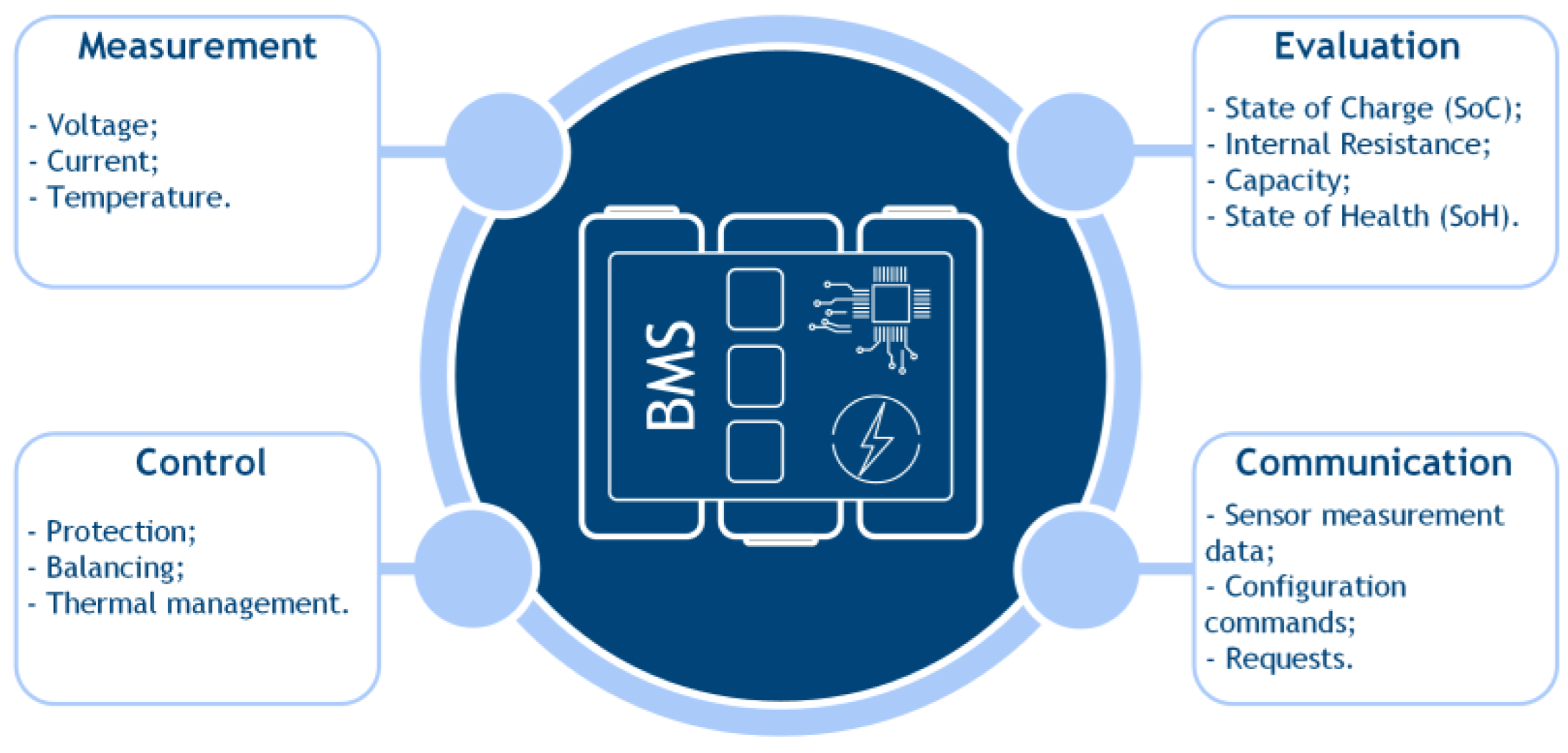
Figure 1. Functions of a BMS.
Energies 16 03255 g001
Figure 2. Switched-capacitor converter: (a) conventional version; (b) improved version proposed in [29].
Energies 16 03255 g002
Figure 3. Control signals for the semiconductors S1 and S2 during two periods.
Energies 16 03255 g003
Figure 4. Operating modes of the SC converter: (a) first stage, T1; (b) second stage, T2.
Energies 16 03255 g004
Figure 5. Double-tiered switched-capacitor converter.
Energies 16 03255 g005
Figure 6. Operating modes of the DTSC converter: (a) first stage, T1; (b) second stage, T2.
Energies 16 03255 g006
Figure 7. Switched capacitor–inductor converter.
Energies 16 03255 g007
Figure 8. Operating modes of the SCI converter: (a) first stage, T1; (b) second stage, T2.
Energies 16 03255 g008
Figure 9. Single inductor converter.
Energies 16 03255 g009
Figure 10. Operating modes of the SI converter: (a) first stage, T1; (b) second stage, T2.
Energies 16 03255 g010
Figure 11. Switched inductor converter.
Energies 16 03255 g011
Figure 12. Operating modes of the SwI converter: (a) first stage, T1; (b) second stage, T2.
Energies 16 03255 g012
Figure 13. Operating modes of the SwI converter: (a) discharging of cell 1; (b) charging of cell 2.
Energies 16 03255 g013
Figure 14. Cuk converter.
Energies 16 03255 g014
Figure 15. Operating modes of the Cuk converter: (a) first stage, T1; (b) second stage, T2.
Energies 16 03255 g015
Figure 16. Operating modes of the Cuk converter: (a) discharging of cell 1; (b) charging of cell 2.
Energies 16 03255 g016
Figure 17. Flyback converter.
Energies 16 03255 g017
Figure 18. Operating modes of the SF converter: (a) discharging of cell 1; (b) charging of cell 2.
Energies 16 03255 g018
Figure 19. Multi-winding transformer converter.
Energies 16 03255 g019
Figure 20. Operating modes of the MWT converter: (a) first stage, T1; (b) second stage, T2.
Energies 16 03255 g020
Figure 21. Comparison of the CC–CC converters for active balancing.
Energies 16 03255 g021
Figure 22. Comparison of the two types of balancing: (a) initial cells’ SoC; (b) final cells’ SoC with passive balance; (c) final cells’ SoC with active balance.
Energies 16 03255 g022
Table 1. Actions of the controlled semiconductors, Sxy.
Vcell1 > Vcell2Vcell1 > Vcell3Vcell2 > Vcell1Vcell2 > Vcell3Vcell3 > Vcell1Vcell3 > Vcell2
TonS1a − S2bS1aS2bS1bS2cS1bS2cS1cS2dS1cS2d
Toff = TTonS2bS1cS2cS1dS2cS1dS2aS1bS2aS1bS2bS1c
Table 2. Comparison of the CC–CC converters for active balancing.
Balancer TypeSwitch
Amounts
Cell
Amounts
Cell
Type
Cell
Capacity
Efficiency
Switched-capacitor [47]4n − 38Li-on15.5 Ah97.73%
Double-tiered capacitor [32]2n1Li-on12 Ah99%
Switched capacitor-inductor [35]2n---89.1%
Single-inductor [36]2(n + 1)1Li-on10 Ah91.5%
Switched-inductor [48]2(n − 1)14LiFePO43.35Ah99.7%
Cuk [41]2(n − 1)1LiPo1 Ah94%
Single flyback [49]2(n + 1)1LiFePO42.65 Ah88%
Multi-winding flyback [46]n4Li-on2.6 Ah73.5%
Disclaimer/Publisher’s Note: The statements, opinions and data contained in all publications are solely those of the individual author(s) and contributor(s) and not of MDPI and/or the editor(s). MDPI and/or the editor(s) disclaim responsibility for any injury to people or property resulting from any ideas, methods, instructions or products referred to in the content.