Abstract
This paper introduces a dual-switchhigh step-up DC-DC power converter. The proposed converter features a high step-up voltage gain, relatively low cumulative stored energy over its inductors, low voltage stress on the active switches, and high efficiency, even at a relatively high duty ratio. An assessment of the proposed converter against conventional boost and a high step-up power converter is presented in terms of steady-state time, voltage gain, stored energy over its inductors, and efficiency. The assessment shows a reduction of 81.25% and 62.5% of stored energy in inductors to comply with the same operational conditions. Simulation and experimental results are provided to validate the benefits of the proposed dual-switch high step-up power converter.
1. Introduction
Nowadays, DC-DC power electronic converters are among the main building blocks in various electrical applications, such as renewable energy integration systems, high-intensity lamp ballasts in automobiles, smart lighting, and small, medium, and high-scale electronic appliances [1,2,3]. According to the literature, in theory, a DC-DC boost power converter with synchronous rectification can be designed to achieve a high step-up voltage gain by properly managing its duty cycle (d or D) [4]. The “conventional Boost” is shown in Figure 1, where the input voltage , input current , and output voltage are indicated. The topology consists of one inductor L, one capacitor C, and a load resistor R. Note that the switching function s is complementary to the switching function . However, in reality, the step-up voltage gain is restricted due to switching losses of semiconductors, equivalent series resistors of inductors and capacitors, and other parasitic effects of the implemented circuit [5,6]. Furthermore, it is well established in the literature that the higher the duty ratio, the higher the reverse-recovery problem. To help alleviate this issue, some topologies have been proposed [7,8]. Their objective is to provide a high step-up voltage gain while maintaining a relatively low-duty cycle. Featuring a high step-up voltage gain, other investigations include the so-called “transformerless DC-DC power converters” [9,10,11]. These studies include (but are not limited to) the cascade boost type power converter, the quadratic boost type [12,13], the capacitor-diode voltage multiplier type [14,15], and the boost type with switched-capacitor technique [16]. Nevertheless, all of these power converter designs are intricate and present relatively high costs. A transformerless DC-DC power converter was proposed in [17], featuring high step-up (HSU) voltage gain. The HSU converter is depicted in Figure 2 and consists of two switches and , two inductors and , an output diode , and a capacitor C. Switches and are controlled simultaneously. The HSU power converter implements the switched-inductor technique, where two inductors with equal inductance values are charged in parallel during the switch-on state and are discharged in series during the switch-off state of the power converter. This technique enables a high step-up voltage gain while avoiding an extreme duty ratio.
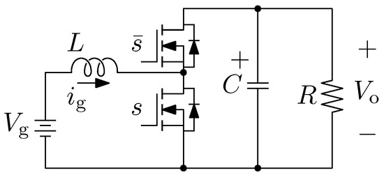
Figure 1.
Conventional boost power converter.
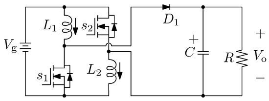
Figure 2.
High step-up (HSU) power converter.
In this paper, a dual-switch high step-up power converter, termed the “Double Dual Super Boost (DDSB)”, is proposed. It is depicted in Figure 3 and features a high step-up voltage gain, low voltage stress on the active switches, and high efficiency (even at a relatively high duty ratio). Additionally, when compared to the conventional boost and the so-called HSU power converters, the DDSB converter has a significantly higher voltage gain. Furthermore, in terms of stored energy over its inductors, the cumulative stored energy is substantially less.
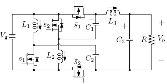
Figure 3.
Proposed high step-up power converter, named the “Double Dual Super Boost (DDSB)”.
Based on the discussion above, the main contributions of this article are summarized as follows:
- A new dual-switch high step-up power converter is proposed. It is identified as the “Double Dual Super Boost”, featuring high step-up voltage gain;
- When compared to the conventional boost and HSU power converters, its cumulative stored energy over its inductors is significantly less;
- Lastly, the DDSB power converter outperforms the conventional boost and HSU power converters featuring significantly less voltage stress over the active switches;
2. Modeling
The proposed topology contains three inductors: , , and ; three capacitors: , , and ; and four transistors: , , , and . It is depicted in Figure 3. Switching functions of transistors and are complementary to the switching functions of transistors and .
In the continuous conduction mode (CCM), the analysis of the switching states leads to two possible equivalent circuits depicted in Figure 4 and Figure 5.
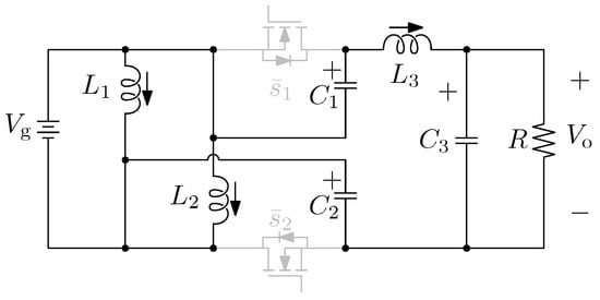
Figure 4.
Equivalent circuit of switching state 1.
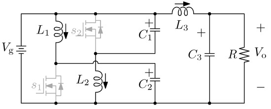
Figure 5.
Equivalent circuit of switching state 2.
2.1. Mathematical Model of the Proposed DDSB Converter
Regarding the mathematical model of the DDSB power converter, it is necessary to take into account both circuits shown in Figure 4 and Figure 5. By applying the standard averaging technique, the following mathematical model is obtained. The average voltage across inductors , , and during one switching cycle is expressed by Equations (1)–(3), respectively.
where , , and correspond to the voltage across each capacitor, and , , and refer to the current through each of the inductors. Notice, the first term of each equation (multiplied by d) corresponds to the voltage across each inductor when the switches and are closed. The second term of each previous equation represents the voltage across each inductor when the switches and are open (multiplied by (1–d)). In the same fashion, the averaging technique can be applied to the current passing through each of the capacitors. By doing so, the average current through capacitors , , and can be expressed as (4)–(6), respectively. It should be noted that corresponds to the output current and is calculated by ().
The set of Equations (1)–(6) is the average dynamic model of the converter. Before analyzing the model, Equations (1)–(6) can be simplified by performing some mathematical manipulations. The simplified equations are rewritten as Equations (7)–(12).
The average dynamic model assumes that the DDSB power converter is operating in CCM.
2.2. DC Components of State Equations or Equilibrium Operating Point
From the dynamic model of the proposed DDSB converter represented by Equations (7)–(12), the equilibrium operating point can be calculated. Considering the small ripple approximation [18], which can be summarized as variables that appear in lowercase in Equations (7)–(12). The lowercase format indicates that these are not constant values. The small ripple approximation considers that changes over the state variables are negligibly small during a single switching cycle. This can be accomplished by selecting an appropriate switching frequency and nominal values of capacitance and inductance for capacitors and inductors, respectively. In the steady state, the derivative of state variables is equal to zero. Therefore, by making Equations (7)–(12) equal to zero and considering the small ripple approximation, the equilibrium of the converter can be found. From Equations (7) and (8), the voltage across the capacitors and can be determined as follows:
Then, the output voltage, which is the same as , can be obtained from (9) as follows:
Finally,
2.3. Selection of Components
The reactive elements of the DDSB converter can be sized following the standard procedure presented in [18], with the design specifications being the maximum current ripple allowed in inductors and the maximum voltage ripple allowed in capacitors. From the equivalent circuits shown in Figure 4 and Figure 5, inductors and can be chosen with the following Equation (18).
where and are the maximum allowed current ripples through and , respectively, and can be obtained as a percentage of the DC (for example, 10% of the DC at the rated power). Equation (18) can be derived relatively simply since inductors and are connected to the input power source when the transistors are closed. Regarding , we may observe that it is connected to the voltage when transistors are closed (see Figure 4 and Figure 5). Hence, their inductances can be selected with Equations (19) and (20).
where is the maximum allowable current ripple through .
In the case of capacitors, from the equivalent circuits shown in Figure 4 and Figure 5, capacitances and can be chosen with the following Equation (21).
where and are the maximum allowable voltage ripple in and , respectively; similar to the current ripple case in the inductors, the maximum voltage ripple can be provided as a percentage of the DC voltage (for example, 0.1% of the DC voltage at the rated power). ’s current is continuous since it belongs to a second-order filter; similar to the Buck or the Cuk converter, the capacitance can be determined with (22),
where is the maximum allowable voltage ripple in , which (in this case) is the same as the output voltage ripple.
2.4. Stored Energy in Inductors
Regarding the conventional boost power converter, its input current ripple is given by Equation (23),
Moreover, the energy that is stored over its pole inductor, defined as , can be determined by Equation (24),
In the case of the HSU power converter, the input current ripple of each inductor can be determined by Equation (25),
In addition, the energy stored over the two inductors, defined as , can be obtained by Equation (26),
In relation to the proposed DDSB converter depicted in Figure 3, it can be determined that the input current ripple over the inductors , , and is expressed by Equation (27),
Furthermore, the stored energy over the three inductors, defined as , can be determined by Equation (28), as follows:
3. Comparative Evaluation
In this section, a comparative performance evaluation of the conventional boost, HSU, and the proposed DDSB is presented. Five main power converter characteristics are investigated and validated: (i) steady-state time, (ii) output voltage (iii) gain ratio, (iv) stored energy over inductors, and (v) efficiency.
3.1. Considerations
Consider that all three power converters are fed with an input voltage of = 20 V. The converters will be supplying power to a resistive load of 100 , which will demand an output power of 100 W ( A) and a switching frequency kHz. The maximum input current ripple is set to 2.1 A, which represents 42% of the input DC. The maximum output voltage ripple is set to 0.8 V, which represents 0.8% of the output voltage.
For internal capacitors, where the output voltage ripple is not affected by these capacitors, the maximum voltage ripple is required to be 0.3% of their DC voltage. In this study, the capacitors and inductors are represented by non-commercial components in the solution of the ripple equations; nevertheless, this is a good approximation of their commercial components.
3.2. Design Parameters
In order to develop a comparative performance evaluation of the conventional boost and HSU versus the proposed DDSB power converter, common design parameters (shown in Table 1) are listed.

Table 1.
Nominal design parameters of all three power converters.
At the same time, and based on the design considerations listed in Table 1, the conventional boost converter requires, for instance, an inductor H to provide an input current ripple A. The complete reactive elements of the conventional boost converter are presented in Table 2.
Table 2.
Conventional boost converter design.
Correspondingly, the HSU converter requires an inductor H to provide an input current ripple A. The complete reactive elements of the HSU converter are shown in Table 3.
Table 3.
HSU converter design.
In the same manner, the DDSB converter requires a capacitor of 10 F to comply with the output voltage ripple of 0.8 V. The complete list of design considerations for the DDSB converter is listed in Table 4.
Table 4.
DDSB converter design.
3.3. Steady-State Time Comparison
In the present case, the steady-state time of the conventional boost, the HSU, and the DDSB power converters is assessed. To this end, the following assumption is made: any power converter will reach steady-state when a variation of ±1% oof the output voltage is measured. Under this assumption, measurements of the output voltage are depicted in Figure 7. Additionally, the collected information is summarized in Table 5.
Table 5.
Steady-state time summary.
From the information presented in Table 5, the lower overshoot voltage is measured in the DDSB converter. However, the conventional boost reaches a steady state faster than both the DDSB and the HSU power converters.
3.4. Output Voltage Comparison
In this case, the output voltage simulation results are depicted in Figure 6. In addition, in order to verify the correctness of the output voltage ripple, a zoom-in of these measurements is shown.
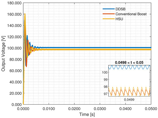
Figure 6.
Comparison of the output voltage of the conventional boost and HSU power converters vs. the DDSB converter.
As observed in Figure 6, the output voltage of the conventional boost and the HSU converters is slightly different from the designed output voltage V. Additionally, the output voltage ripple of the conventional boost and the HSU converters appears slightly below that of the DDSB. Hence, a small correction of the duty cycle should be made. This small change will generate simulation results presented in Figure 7, where all three traces feature a reasonable match. It should be noted that in order to obtain an output voltage of = 100 V, the duty cycle values for the conventional boost, the HSU, and the DDSB are , , and , respectively. As depicted in Figure 7, now all three traces of the output voltage ripple are essentially on top of each other and comply with the design specification of the output voltage ripple. In summary, the DDSB outperforms both the conventional boost and the HSU converters in terms of output voltage gain. As shown, a reduction in the duty ratio of 14.2% and 1% is obtained, respectively, while synthesizing the same output voltage.
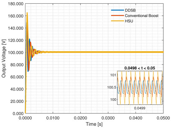
Figure 7.
Comparison of the output voltage of the conventional boost (), HSU (), and DDSB () power converters.
3.5. Gain Ratio
This subsection evaluates the gain ratio over an operation range of the conventional boost, the HSU, and the DDSB power converters. As shown in Figure 8, a duty cycle range from [0.5 to 0.85] is taken into account. It can be observed that the proposed DDSB significantly outperforms the conventional boost and even surpasses the HSU by 1% in terms of its voltage gain. Note that the added red-colored marks indicate the necessary duty cycle that outputs 100 V in both power converters.
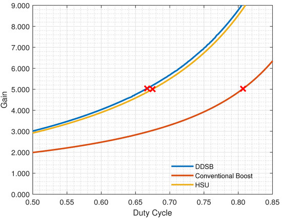
Figure 8.
Comparison of the gain ratio of the conventional boost and HSU vs. DDSB power converters.
3.6. Stored Energy over Inductors
On the one hand, the inductors of any power converter, in order to operate, have to store some amount of energy. Moreover, it must be compliant with a specific design. This energy value is directly related to the inductor size and its operational conditions. On the other hand, a reduction in the size of inductors will have a favorable impact on reducing the power converter cost. In this article, the stored energy over the inductors of the conventional boost, HSU, and DDSB power converters is assessed.
First, using Equation (24), the stored energy over the inductor of the conventional boost is determined. Second, using Equation (26), the stored energy over the inductors of the HSU is computed. Lastly, Equation (28) is used to calculate the stored energy in the inductors of the DDSB. Simulation results of the stored energy over the inductors of all three power converters with respect to their duty cycle are depicted in Figure 9. Similarly, simulation results of the stored energy with respect to their gain ratio are illustrated in Figure 10. Notice that the added red marks depict the necessary stored energy to provide an output voltage of 100 V in all three power converters. When the conventional boost is compared to the DDSB, a reduction of 81.25% of stored energy over the inductors is obtained. Similarly, by comparing the HSU to the DDSB, a reduction of 62.50% of stored energy over the inductors is calculated. As shown, in Figure 9 and Figure 10, the DDSB outperforms the conventional boost and the HSU power converters, featuring significantly less stored energy over its inductors.
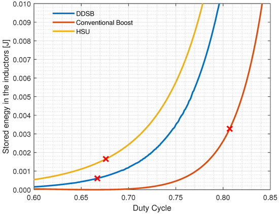
Figure 9.
Stored energy in the inductors of the conventional boost, HSU, and DDSB power converters with respect to the duty cycle d.
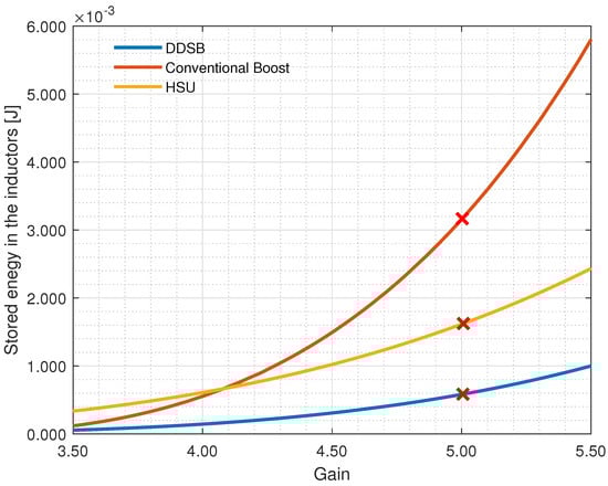
Figure 10.
Stored energy in the inductors of the conventional boost and HSU vs. DDSB power converters with respect to the gain ratio.
3.7. Efficiency
Efficiency is one of the main factors in the development and investigation of DC–DC power converters. It is defined as , where is the input power, and accounts for power losses due to switching and conduction. In this article, is accounted for using standard procedures presented in [4]. Simulation results of the efficiency of all three power converters are shown in Figure 11. According to the traces shown in Figure 11, the DDSB outperforms both the conventional boost and the HSU in terms of efficiency. The red marks indicate the efficiency values when all three power converters output 100 V. At this operating point, the DDSB demonstrates an improvement of 1% and 0.75% in efficiency compared to the conventional boost and the HSU, respectively. As shown, the DDSB outperforms the conventional boost and HSU converters in terms of efficiency.
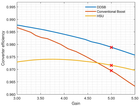
Figure 11.
Efficiency of the conventional boost and HSU vs. DDSB power converters, taking into account a fixed load.
4. Experimental Results
To validate the operation of the proposed DDSB power converter, an experimental prototype was built. Its design parameters are indicated in Table 1 and Table 4. The converter prototype is depicted in Figure 12. In this section, three main characteristics are validated: (i) validation of the input variables, such as the input current , input voltage , and terminal voltage of transistor , (ii) validation of the output variables, output current , output voltage , and terminal voltage of transistor , and (iii) validation of the inductor currents and .
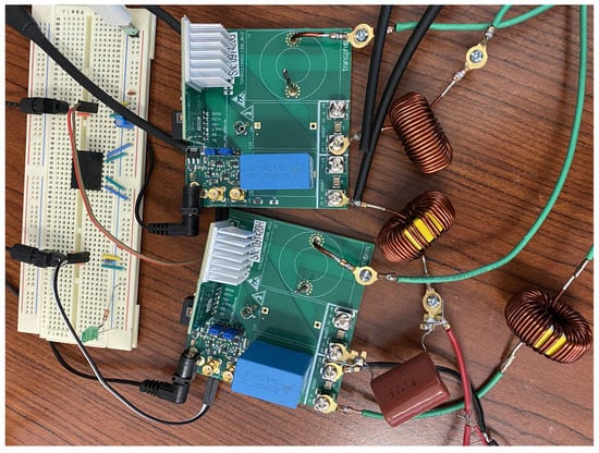
Figure 12.
Prototype picture.
4.1. Validation of Input Variables
First, the input voltage , input current , and a single switching signal are presented in Figure 13 based on simulation results. Note that while the y-axis for input current is on the left side of Figure 13, the y-axis for input voltage and switching signal is on the right side. Similar traces obtained from measurements of the experimental prototype are shown in Figure 14. Traces shown in Figure 13 and Figure 14 feature a reasonable match.
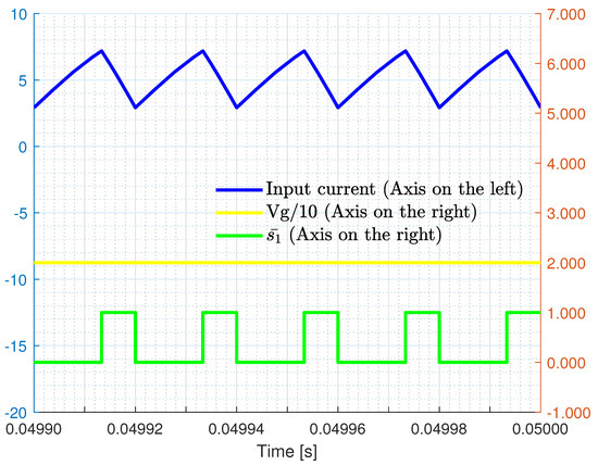
Figure 13.
From the top to the bottom: input current (blue trace), input voltage (yellow trace), and switching signal (green trace) of DDSB.
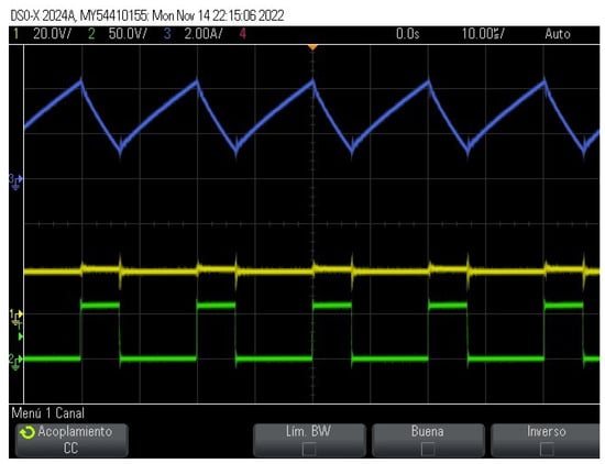
Figure 14.
From the top to the bottom: input current (blue trace), input voltage (yellow trace), and terminal voltage of transistor V (green trace) of the DDSB power converter.
4.2. Validation of Output Variables
Measurements of the output voltage , output current , and switching signal obtained from the simulations results are portrayed in Figure 15. Regarding Figure 15, the input current y-axis is placed on the left side, and the y-axis for the output voltage and switching signal are located on the right-side. The output current features a DC offset of 4 A.
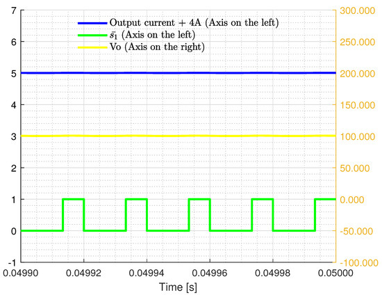
Figure 15.
From the top to the bottom: output current (blue trace), output voltage (yellow trace), and switching signal (green trace) of DDSB.
In the same fashion, measurements of the output voltage , output current , and terminal voltage of transistor V obtained from the experimental prototype are depicted in Figure 16. By comparing Figure 15 and Figure 16, a good match between the simulation and experimental results is observed.
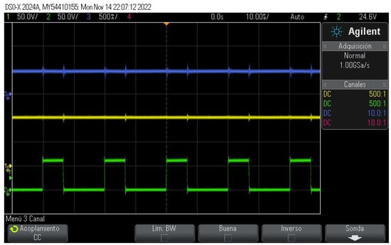
Figure 16.
From the top to the bottom: output current (blue trace), output voltage (yellow trace), and terminal voltage of transistor V (green trace) of DDSB.
4.3. Validation of Inductor Currents and
Simulation results of measurements for inductor currents and are shown in Figure 17. An offset of 3A was set to inductor current , while an offset of 2A was set to inductor current . These currents are depicted along with the switching signal utilized in former figures. In this case, all y-axes are on the left side of Figure 17.
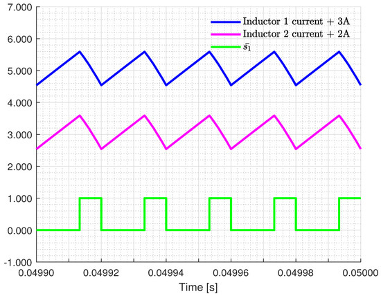
Figure 17.
From the top to the bottom: inductor current (blue trace), inductor current (pink trace), and switching signal (green trace) of DDSB.
Similarly, experimental measurements of inductor currents and , as well as the terminal voltage of transistor V, are presented in Figure 18. As shown, a good match is obtained in terms of the average value, current ripple , and slopes.
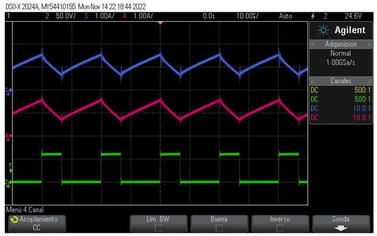
Figure 18.
From the top to the bottom: inductor current (blue trace), inductor current (pink trace), and terminal voltage of transistor V (green trace) of DDSB.
5. Conclusions
This paper introduced a dual-switch high step-up DC-DC power converter, called the “DDSB”. The particular features of the proposed DDSB are a high step-up voltage gain, relatively low cumulative stored energy over its inductors, low voltage stress on the active switches, and high efficiency even at a relatively high duty ratio. A comparative assessment showed that the DDSB power converter outperforms the conventional boost and the HSU power converters under the same operational conditions, as follows: (i) the DDSB featured a reduction of 14.2% and 1% in the duty ratio to achieve the same output voltage; (ii) the DDSB showed a reduction of 81.25% and 62.50% of stored energy in the inductors with respect to the conventional boost and the HSU, respectively. As a consequence, the physical size of the DDSB was reduced; and (iii) when the conventional boost and the HSU were compared against the DDSB, improvements of 1% and 0.75% in terms of efficiency were obtained, respectively. Furthermore, the principle of operation and the mathematical model of the DDSB were also presented. Finally, experimental results were provided to validate the performance of the proposed converter.
6. Future Work
It would be feasible to conduct further investigations if the constraint of keeping all inductances and capacitances at the same value were released. By doing so, it would be possible to explore alternatives to optimize the power converter’s input current and to develop an approach to optimize the energy stored in the converter. Moreover, it could be possible to investigate advanced control techniques applied to this converter and to conduct a sensitivity study in-depth regarding the steady-state time of the DDSB power converter in terms of its inductors, capacitors, and switching frequency. Nevertheless, at this stage, these possible improvements are beyond the scope of this research.
Author Contributions
H.R.R.-C., A.V.-G. and J.C.R.-C. contributed to the conceptualization of the article; H.R.R.-C., A.V.-G., J.C.R.-C., H.A.G. and B.B. contributed to the formal analysis; H.R.R.-C., A.V.-G., J.C.R.-C. and H.A.G. contributed to the methodology; A.V.-G. and J.C.R.-C. contributed to the funding acquisition; H.R.R.-C. and A.V.-G. contributed to the investigation; A.V.-G. and J.C.R.-C. contributed to the project administration; A.V.-G., J.C.R.-C., H.A.G. and B.B. contributed to the software; H.R.R.-C., A.V.-G., J.C.R.-C., H.A.G. and B.B. contributed to the validation; H.R.R.-C. contributed to the visualization; H.R.R.-C., A.V.-G. and J.C.R.-C. contributed to the writing of the original draft, reviewing, and editing; All authors have read and agreed to the published version of the manuscript.
Funding
The authors would like to thank Universidad Panamericana for their support through the program “Fomento a la Investigación UP 2022”, and project “Estudio de topologías de convertidores de cd-cd” UP–CI–2022–GDL–06–ING.
Data Availability Statement
Not applicable.
Acknowledgments
The authors gratefully acknowledge the support of Universidad Panamericana Campus Guadalajara, in Zapopan, Jalisco, México.
Conflicts of Interest
The authors declare no conflict of interest.
Abbreviations
The following abbreviations are used in this article:
| HSU | high step-up |
| DDSB | double dual super boost |
| CCM | continuous conduction mode |
References
- Forouzesh, M.; Shen, Y.; Yari, K.; Siwakoti, Y.P.; Blaabjerg, F. High–Efficiency High Step–Up DC–DC Converter with Dual Coupled Inductors for Grid–Connected Photovoltaic Systems. IEEE Trans. Power Electron. 2018, 33, 5967–5982. [Google Scholar] [CrossRef]
- Blaabjerg, F.; Chen, Z.; Kjaer, S. Power electronics as efficient interface in dispersed power generation systems. IEEE Trans. Power Electron. 2004, 19, 1184–1194. [Google Scholar] [CrossRef]
- Forouzesh, M.; Siwakoti, Y.P.; Gorji, S.A.; Blaabjerg, F.; Lehman, B. Step–Up DC–DC Converters: A Comprehensive Review of Voltage–Boosting Techniques, Topologies, and Applications. IEEE Trans. Power Electron. 2017, 32, 9143–9178. [Google Scholar] [CrossRef]
- Mohan, N. Power Electronics: A First Course; John Wiley & Sons: Hoboken, NJ, USA, 2012; pp. 1–270. [Google Scholar]
- Walczak, M.; Bychto, L. Influence of Parasitic Resistances on the Input Resistance of Buck and Boost Converters in Maximum Power Point Tracking (MPPT) Systems. Electronics 2021, 10, 1464. [Google Scholar] [CrossRef]
- Janke, W.; Baczek, M.; Kraśniewski, J.; Walczak, M. Large–signal input characteristics of selected DC–DC switching converters Part I. Continuous conduction mode. Arch. Electr. Eng. 2020, 69, 739–750. [Google Scholar]
- Hassan, W.; Lu, D.D.; Xiao, W. Single–Switch High Step–Up DC–DC Converter with Low and Steady Switch Voltage Stress. IEEE Trans. Ind. Electron. 2019, 66, 9326–9338. [Google Scholar] [CrossRef]
- Hsieh, Y.; Chen, J.; Liang, T.; Yang, L. Analysis and implementation of a novel single–switch high step–up DC–DC converter. IET Power Electron. 2012, 5, 11–21. [Google Scholar] [CrossRef]
- Mumtaz, F.; Yahaya, N.Z.; Meraj, S.T.; Singh, N.S.S.; Abro, G.E.M. A Novel Non-Isolated High-Gain Non-Inverting Interleaved DC-DC Converter. Micromachines 2023, 14, 585. [Google Scholar] [CrossRef] [PubMed]
- Solis-Rodriguez, J.; Rosas-Caro, J.C.; Alejo-Reyes, A.; Valdez-Resendiz, J.E. Optimal Selection of Capacitors for a Low Energy Storage Quadratic Boost Converter (LES–QBC). Energies 2023, 16, 2510. [Google Scholar] [CrossRef]
- Alejo-Reyes, A.; Rodríguez, A.; Mendoza, A.; Rosas-Caro, J.C. Numerical Optimization of the Capacitors Selection in the MSBA Converter to Reduce the Output Voltage Ripple. Symmetry 2022, 14, 2383. [Google Scholar] [CrossRef]
- López–Santos, O.; Varón, N.L.; Rosas–Caro, J.C.; Mayo–Maldonado, J.C.; Valdez–Reséndiz, J.E. Detailed Modeling of the Low Energy Storage Quadratic Boost Converter. IEEE Trans. Power Electron. 2022, 37, 1885–1904. [Google Scholar]
- Loera-Palomo, R.; Morales-Saldaña, J.A.; Rivero, M.; Álvarez-Macías, C.; Hernández-Jacobo, C.A. Noncascading Quadratic Buck–Boost Converter for Photovoltaic Applications. Micromachines 2021, 12, 984. [Google Scholar] [CrossRef] [PubMed]
- Meraj, M.; Bhaskar, M.S.; Iqbal, A.; Al–Emadi, N.; Rahman, S. Interleaved Multilevel Boost Converter with Minimal Voltage Multiplier Components for High–Voltage Step–Up Applications. IEEE Trans. Power Electron. 2020, 35, 12816–12833. [Google Scholar] [CrossRef]
- Dalla Vecchia, M.; Van den Broeck, G.; Ravyts, S.; Driesen, J. Novel Step–Down DC–DC Converters Based on the Inductor–Diode and Inductor–Capacitor–Diode Structures in a Two–Stage Buck Converter. Energies 2019, 12, 1131. [Google Scholar] [CrossRef]
- Rosas–Caro, J.C.; Mayo–Maldonado, J.C.; Valdez–Resendiz, J.E.; Alejo–Reyes, A.; Beltran–Carbajal, F.; López–Santos, O. An Overview of Non–Isolated Hybrid Switched–Capacitor Step-Up DC–DC Converters. Appl. Sci. 2022, 12, 8854. [Google Scholar] [CrossRef]
- Yang, L.; Liang, T.; Chen, J. Transformerless DC–DC Converters with High Step–Up Voltage Gain. IEEE Trans. Ind. Electron. 2009, 56, 3144–3152. [Google Scholar] [CrossRef]
- Erickson, R.W.; Maksimović, D. Fundamentals of Power Electronics, 2nd ed.; Kluwer: Boston, MA, USA, 2004. [Google Scholar]
- Simscape Toolbox Release R2022b. In Matlab; The MathWorks Inc.: Natick, MA, USA, 2023.
- Electrical Engineering Software R4.6.8. In PLECs; PLEXIM Inc.: Zürich, Switzerland, 2023.
Disclaimer/Publisher’s Note: The statements, opinions and data contained in all publications are solely those of the individual author(s) and contributor(s) and not of MDPI and/or the editor(s). MDPI and/or the editor(s) disclaim responsibility for any injury to people or property resulting from any ideas, methods, instructions or products referred to in the content. |
© 2023 by the authors. Licensee MDPI, Basel, Switzerland. This article is an open access article distributed under the terms and conditions of the Creative Commons Attribution (CC BY) license (https://creativecommons.org/licenses/by/4.0/).