Article

Modeling of Changes in the Resistivity of Semi Insulating Gallium Phosphide under the Influence of Lighting

Faculty of Electronics, Military University of Technology, gen. Sylwestra Kaliskiego 2, 00-908 Warsaw, Poland
*
Author to whom correspondence should be addressed.
Energies 2023, 16(4), 1725; https://doi.org/10.3390/en16041725
Submission received: 29 December 2022 / Revised: 23 January 2023 / Accepted: 7 February 2023 / Published: 9 February 2023

Abstract

:
The article presents the results of a simulation of changes in gallium phosphide (GaP) resistivity under the influence of lighting. The adopted model of the defect structure is presented along with the defect parameters. Initial conditions created on the basis of a tested material sample, labeled GaP-1, made of monocrystals of semi-insulating gallium phosphide (SI GaP), are presented. The simulation methodology and the created model of the kinetics equations are described. As a result of the simulation, the values of the photocurrent and the electron-hole pair generation coefficient G were assigned to data obtained experimentally depending on the carrier lifetime coefficient τ. Changes in resistivity and concentration of electrons and holes in the bands for gallium phosphide with a structure consisting of five defects are presented. The proposed simulation method can be used to calculate switch-on and -off times and photocurrent values for the semiconductor materials used to construct PCSS (photoconductive semiconductor switches) and other electronic devices.

1. Introduction

Semiconductor materials are the basis of systems used in electronics and power engineering and, in recent years, there has been a growing interest in the use of optical semiconductor devices [1]. One such device is the PCSS (photoconductive semiconductor switch). The PCSS is an electrical switch whose operating principle is based on the phenomenon of photoconduction. Excitation of semiconductor material by a beam of light generates excess charge carriers in the form of electron-hole pairs and changes the semiconductor material’s conductivity by several orders of magnitude [2] in times of nanoseconds or picoseconds [3]. In the blocking state, PCSS switches can work at voltages up to 100 kV, while in the conducting state, the flowing current reaches values as high as 1 kA [4,5]. The operation frequency of these devices depends mainly on their turn-off time, reaching values of the order of 1 kHz [4].
The problem of improving the operating parameters of PCSS and other semiconductor-based devices has been the subject of research by many research groups in recent years. The improvement of a semiconductor device’s properties can be achieved by improving the device construction technology or by improving the properties of the semiconductor material [6,7,8,9]. This article focuses on the latter problem. One such approach is compensating for defects created during the production process of the semiconductor material. The concentration of these defects affects the resistivity of the material and is not a linear function. A group of particular interest for constructing PCSSs are semiconductor materials with a wide forbidden band gap [10,11,12], which include gallium nitride (GaN) [13,14], silicon carbide (4H-SiC and 6H SiC) [15,16,17], and gallium phosphide (GaP) [18]. The parameters of these materials depend on the structure and concentration of defects occurring in their crystal lattice, among which we can distinguish native defects and admixtures. The first group includes Schottky defects (lack of an atom in a node of the crystal lattice) and Frenkel defects (displacement of an atom into an interstitial position); while admixtures are foreign atoms introduced into the crystal lattice and can be divided into substitutes and internodes.
One of the methods for testing defects in semiconductor materials is Photo-Induced Transient Spectroscopy (PITS). The tested material is illuminated by a light pulse, filling the defect centers with an excess of electrons or holes. The number and type of defects are determined on the basis of the recorded photocurrent relaxation time courses caused by the thermal emission of the charge carriers following the end of the light pulse. High-Resolution Photoinduced Transient Spectroscopy (HRPTS) is used to study deep defect centers. The results are obtained by applying the Laplace procedure [19,20,21,22].
The article presents simulations of changes in the resistivity of gallium phosphide (GaP) under the influence of lighting, depending on the concentration of the assumed defect centers. The values of the electron-hole pair generation coefficient G and the peak photocurrent values obtained from the simulations were compared with those obtained experimentally from a sample fabricated from monocrystals of semi-insulating gallium phosphide (SI GaP). The results of material simulation with the presented method can be used to calculate photocurrent values and switch-on and -off times of the materials used to build PCSS and other electronic devices.

2. Material Properties

The calculations were performed for a material model in which the existence of five defects was assumed: two shallow donor centers, one deep donor, one shallow acceptor center, and one deep acceptor center. The adopted energy model is presented in Figure 1.
The simulations were carried out for a temperature of 300 K, so the value of the forbidden gap was constant and equaled 2.26 eV. In the adopted model, the shallow donors were at the levels of 0.085 eV and 0.11 eV from the bottom of the conduction band. The first shallow donor was associated with silicon atoms in the gallium subnetwork, while the second was bound to sulfur atoms in the phosphorus sublattice. The shallow acceptors at the level of 0.055 eV from the top of the valence band are the carbon atoms in the phosphorus sublattice and they are the main acceptors in GaP single crystals produced by the Czochralski method. A defect with an energy of 1.035 eV in relation to the bottom of the conduction band was assumed as a deep donor, which can be attributed to the doubly ionized state of phosphorus charge in the gallium sublattice. A deep acceptor is a defect located at the level of 0.85 eV above the top of the valence band; the origin of this center is currently not well studied. Table 1 presents the parameters of the defect centers adopted during the simulation.
As initial conditions for solving the kinetics equations, it was assumed that the simulated material and the tested gallium phosphide sample had the same resistivity in the state without lighting, at the level of 1.86 × 10¹⁰ Ωcm. The test sample marked with GaP-1 was 2 mm wide, 1 mm thick, and 10 mm long. Resistivity measurements of the unilluminated sample were carried out using the METREL MI 3210 TeraOhm XA meter, serving as a source of DC voltage, as well as a meter of both current and resistance. This allows for current measurements from 0.1 nA up to 5 nA with a supply voltage in the range of 50 V to 10 kV. The investigation was carried out for the wavelength of λ = 500 nm, corresponding to an absorption coefficient α equal to 18,224 cm−1 [25], with the electric field strength between the sample electrodes at the level of 52 kV/cm, corresponding to a voltage value of 10 kV.

3. Simulation Procedures

In order to meet the initial condition of the material resistivity value without lighting, in the first step of the simulation, the change in the value of this parameter depending on the concentration of the accepted defects was examined. The resistivity of the unlit material ρ0 was calculated from the relationship:
ρ 0 = 1 σ 0 = 1 q n 0 μ n + p 0 μ p
where σ0 is the conductivity of the unlit material, q is an elementary charge, μn and μp are the mobility of electrons and holes, respectively, and n0 and p0 are the concentrations of the electron and holes of unlit material, determined from the equilibrium equation [26]. For the simulation of the material, the mobilities of the electrons and holes were assumed to be 250 and 150 cm2V−1s−1, respectively [27].
In the next step, photocurrent peaks and changes in the concentration of electrons and holes in the conduction and valence bands, respectively, were examined. For this purpose, the system of kinetics Equations (2)–(8) was solved based on previous works [26]:
d n t d t = e S D 1 n S D 1 t n t c S D 1 N S D 1 n S D 1 t + e S D 2 n S D 2 t n t c S D 2 N S D 2 n S D 2 t + e D D n D D t n t c D D N D D n D D t n t τ + G ,
d p t d t = e S A N S A n S A t p t c S A n S A t + e D A N D A n D A t p t c D A n D A t p t τ + G ,
d n S D 1 t d t = e S D 1 n S D 1 t + n t c S D 1 N S D 1 n S D 1 t ,
d n S D 2 t d t = e S D 2 n S D 2 t + n t c S D 2 N S D 2 n S D 2 t ,
d n D D t d t = e D D n D D t + n t c D D N D D n D D t ,
d p S A t d t = e S A N S A n S A t p t c S A n S A t ,
d p D A t d t = e D A N D A n D A t p t c D A n D A t ,
where n(t) and p(t) denote the concentration of excess electrons and holes in the bands, NSD1, NSD2, NDD, NDA, and NSA denote the assumed concentration of defects: shallow donor 1, shallow donor 2, deep donor, deep acceptor, and shallow acceptor, while nSD1, nSD2, nDD, nDA, and nSA denote the change of concentration at the selected defect level over time, respectively. eSD1, eSD2, eDD, eDA, and eSA are the thermal emission rate coefficients of the respective defect centers. The electron capture ratios for the respective defect sites are designated as cSD1, cSD2, and cSA, while the hole capture ratios for the respective defects are designated as cDD and cDA. The coefficient τ denotes the lifetime of the carriers, while the factor G denotes the generation coefficient of electron-hole pairs. Simulations were carried out for the values of the generation factor G determined on the basis of experimental tests of the GaP-1 sample in the assumed uncertainty range, depending on the carrier lifetime τ. The material factors γn and γp needed to calculate thermal emission factors and capture coefficients for electrons and holes were assumed to be equal to 2.57 × 10²¹ and 2.70 × 1021 cm−2s−1K−2, respectively [27]. Thermal emission factors were calculated using the formula:
e n , p = σ n , p γ n , p T 2 exp E a n , p k B T
where σn,p denote capture cross-sections for electrons (n) or holes (p), T is the absolute temperature assumed to be 300 K, Ean,p is the activation energy of electron emission (n) from a particular type of defect center with respect to the bottom of the conduction band or activation energy of hole emission (p) from a particular type of defect center in relation to the top of the valence band, and kB is Boltzmann’s constant. The capture rates for a given type of defect center are represented by capture coefficients cn and cp for electrons and holes, respectively, and are defined as:
c n , p = σ n , p ν n , p
where νn,p are average electron (n) and hole (p) thermal speeds, equal to 2 × 10⁷ and 1.3 × 107 cm1s−1, respectively [27]. The values of the adopted defect concentration coefficients, the rates of thermal emission, and the capture of electrons and holes are presented in Table 2.
Simulations were performed using the Matlab R2020a software and the ode23 procedure was used to solve the kinetics equations. In the simulation, an illumination time equal to 300 ns was assumed, in which the concentrations in the bands reach a steady state. In order to check the characteristics of the sample after switching off the lighting and to investigate the potential switch-off time of an element constructed with the use of simulated material, simulations were carried out for the next 5 μs.

4. Results

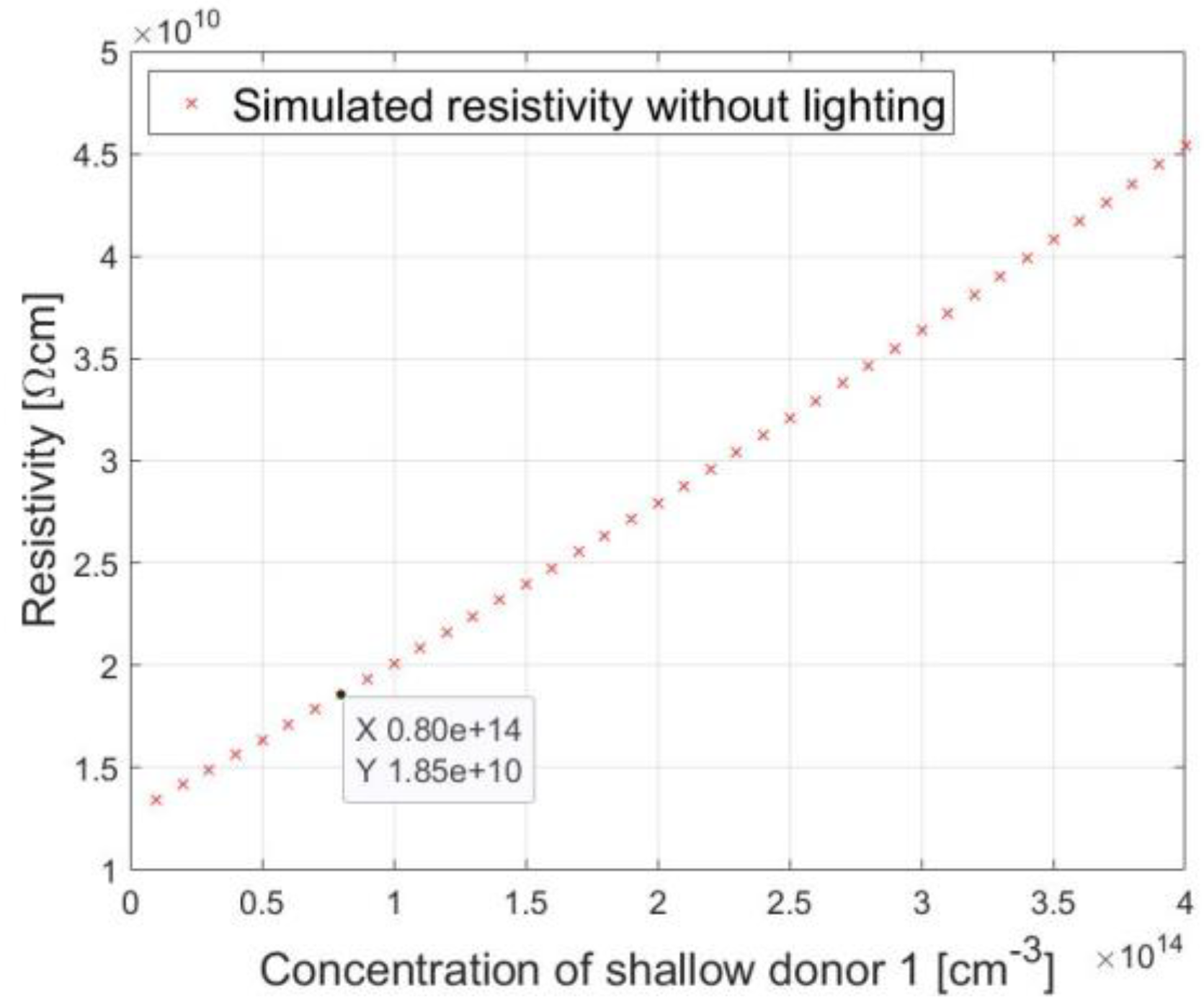
The simulations of the material resistivity in the absence of lighting were carried out depending on the concentration of the defect SD1 in the range from 0.1 to 2.0 × 1014 cm−3, assuming the values of the defect concentration respectively SD2, DD, DA, and SA were 1.3 × 10¹⁴, 3.4 × 10¹⁴, 3.3 × 10¹⁵, 2.8 × 1014 cm−3, respectively. The results are shown in Figure 2. The results show that for a concentration of 0.8 × 1014 cm−3, the resistivity of the material reaches the value of 1.858 × 10¹⁰ Ωcm, which is a satisfactory accuracy for the next step of accumulation.
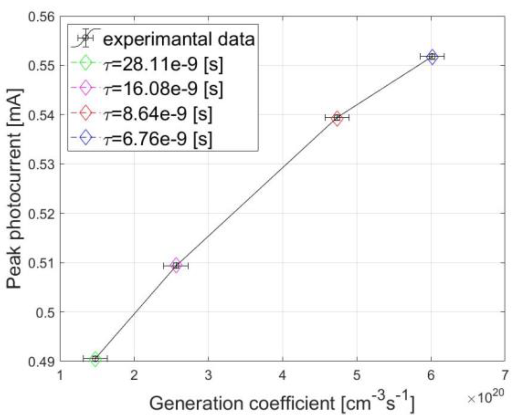
The maximum photocurrent measurements were made in a system consisting of the previously mentioned voltage source and the studied PCSS sample GaP-1 and a 21 MΩ resistor connected in series. Voltage drops across the resistor, as well as the system’s response to the impulse switching the sample into a conduction state, were recorded using an oscilloscope. The optical switching pulse was generated by a tunable laser operating at a frequency of 10 Hz. Maximum photocurrent values were obtained after averaging 32 sample responses to the laser optical pulse and were equal to 0.491, 0.509, 0.539, and 0.552 mA corresponding to the values of the laser power 1.5, 2.6, 4.8, and 6.1 mW, with uncertainty ranges of ±0.25 mW. Using the procedure presented in ref. [26], the values of the generation coefficient G corresponding to the successive laser power were calculated as 1.480 × 10²⁰, 2.565 × 10²⁰, 4.736 × 10²⁰, and 6.018 × 1020 cm−3s−1, with uncertainty ranges of ±0.1628 × 1020 cm−3s−1. As a result of the simulation, the values of the photocurrent and the electron-hole pair generation coefficient G were assigned to the experimental data depending on the carrier lifetime coefficient τ. The carrier lifetime obtained by simulation was between 28.11 to 6.76 ns. The results are shown in Figure 3.
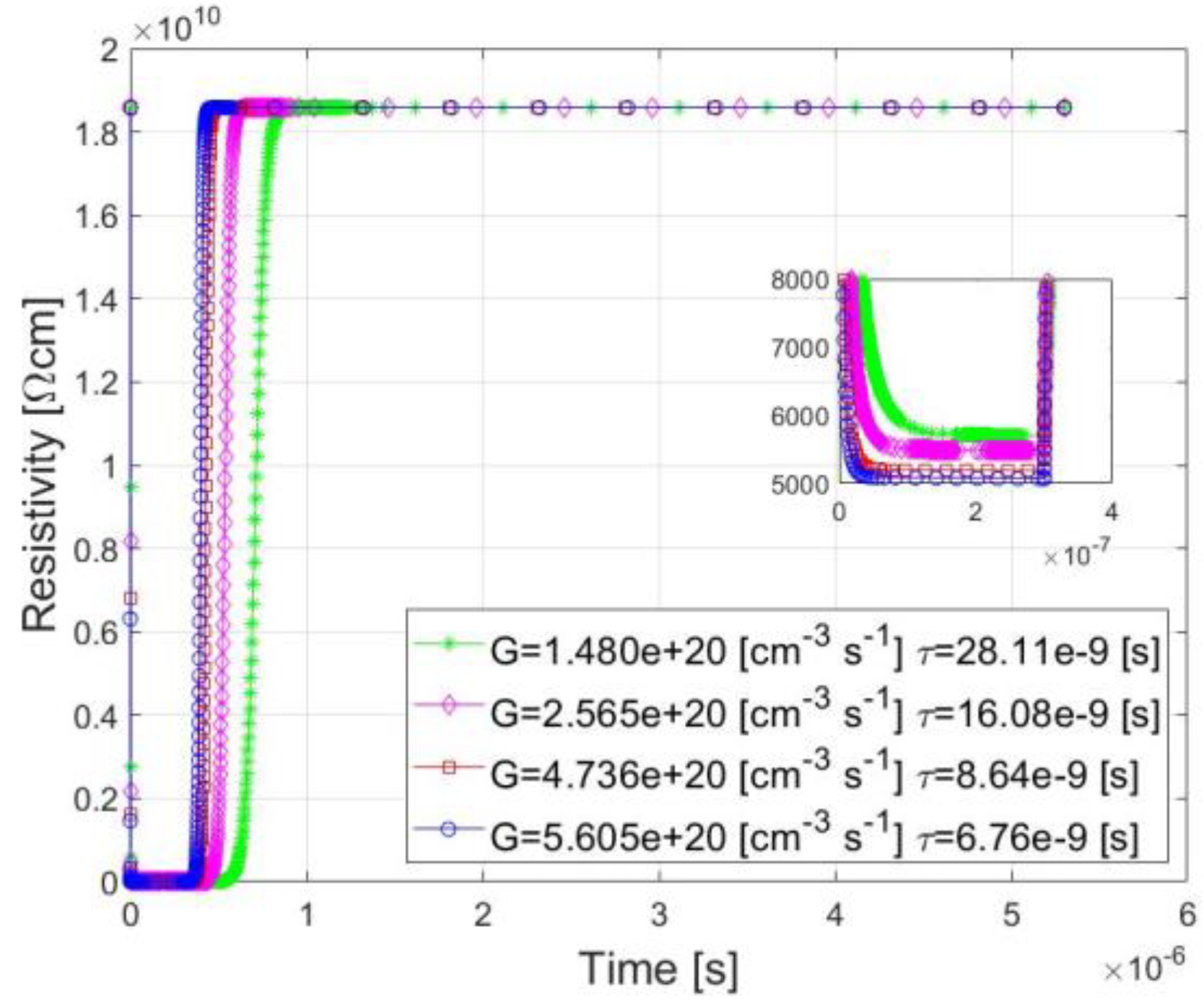
In Figure 4, we can see that, as the generation coefficient of electron-hole pairs increases, the resistivity decreases and the time needed for the resistivity of the material to return to its original value decreases. The shape of the waveform for different values of the coefficient is similar. The resistivity of the material when illuminated is reduced by seven orders of magnitude from about 1.8 × 10¹⁰ to 5 × 10³ Ωcm. After the light source is turned off, the resistivity of the material returns to the value before illumination after 150 to 700 ns. In the inset, we can see that the time needed to reach a steady state is in the range of 50 to 100 ns.
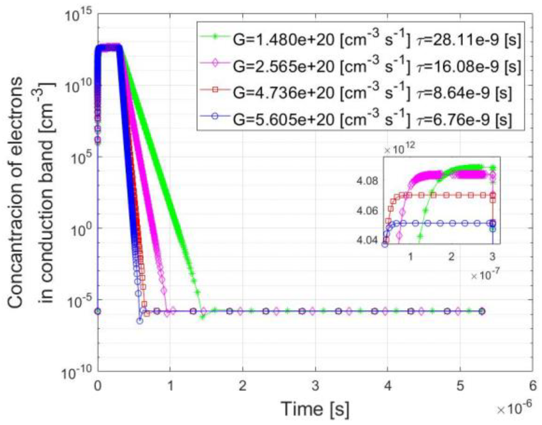
Analyzing Figure 5, we can see in the insert that with the increase in the G coefficient, the time needed to reach a steady state of electron concentration in the conduction band decreases from about 270 ns, for a G coefficient equal to 1.48e + 20 cm−3s−1, to 65 ns for a G coefficient equal to 5.605e + 20 cm−3s−1. We can also see that, when the illumination source is turned off, the electron concentration decreases by an order of magnitude by approximately 16 to 64 ns depending on the generation coefficient of the electron-hole pairs. The time needed for the electron concentration in the conduction band to return to its original value decreases as the generation factor G increases and is in the range of about 1300 to 300 ns.
Figure 6 shows that the increase in the G coefficient is accompanied by a proportional increase in the maximum concentration of holes in the valence band. It can also be seen that, after switching off the illumination source, the concentration of holes decreases by an order of magnitude every 55 ns, regardless of the generation coefficient of electron-hole pairs. The steady state of hole concentration in the valence band is obtained after 15 ns regardless of the G coefficient value.
Figure 5 and Figure 6 show that, regardless of the electron-hole pairs generation coefficient value, the times of rise and fall of the hole concentration in the valence band are smaller than those obtained for the concentration of electrons in the conduction band. This means that the potential turn-on and turn-off times of the GaP-1 sample depend mainly on the parameters of the donor-type defect centers. This information can be useful in the manufacturing process of semiconductor materials to compensate for selected defects at the appropriate level in order to obtain the selected resistivity and appropriate turn-on and turn-off times.

5. Conclusions

The article presents the simulation results for gallium phosphide material under the influence of lighting. Changes in resistivity and concentration of electrons and holes in the bands for gallium phosphide with a structure consisting of five defects were presented. The model of the defect structure of the material and the created system of kinetics equations for the case of five selected defects were shown. The simulation methodology was discussed, and simulation results were compared with the experimentally tested sample designated as GaP-1.
Simulated values of the photocurrent and the electron-hole pair generation coefficient G were assigned to the experimental data depending on the carrier lifetime coefficient τ. From the analysis of the waveforms of the concentration of holes in the valence band, we can conclude that, with the increase in the generation coefficient G, the maximum concentration of holes in the valence band increases. For different values of the electron-hole pair generation coefficient, similar resistivity changes were observed. After the light source is turned off, the resistivity of the simulated material and concentrations of electrons and holes in respected bands returns to their values before illumination after 150 to 700 ns. These results may be satisfactory for PCSS and other electronic devices, however, it would be necessary to verify the on and off times of the element made of the simulated material with new samples and experimental data. The experimental results and assigned simulation results are presented in Table 3, where ρmin is the minimum value of the resistivity, and on and off are the time of the resistivity decrease to the minimum value from the moment the laser is turned on and the time of the resistivity return to the original value from the moment the laser is turned off, respectively.
The purpose of the simulation method presented in the article is to determine the parameters of the semiconductor material in the state without illumination and after illumination. The defects arising in a semiconductor material depend on the method and course of the technological process of their production. Comparing the experimental results of the produced material with the proposed method of simulation will allow information on what parameters should be varied in order to obtain a material with the desired properties to be obtained. This method can also be used to study the conditions of the formation of selected defect centers.
The material designed in accordance with the presented simulation method may, in fact, be characterized by certain deviations in the parameters achieved. Nevertheless, the simulation methodology demonstrated can be helpful in the design of PCSSs and other electronic devices using semiconductor materials intended for use in electronics and power engineering systems.

Author Contributions

Conceptualization, M.S.; methodology, M.S. and K.P.; software M.S., B.P. and K.P.; validation P.P. and W.K.; formal analysis, K.P. and B.P.; investigation, K.P., B.P., P.P. and W.K.; writing—original draft preparation, K.P. and B.P.; writing—review and editing, K.P. and M.S.; visualization, K.P.; funding acquisition, B.P. and M.S. All authors have read and agreed to the published version of the manuscript.

Funding

This work was financed by the Military University of Technology under research project UGB 22-850.

Data Availability Statement

Experimental data is available upon request.

Acknowledgments

The authors would like to thank Pawel Kaminski for helping to carry out experimental measurements on the sample used in the article.

Conflicts of Interest

The authors declare no conflict of interest.

References

  1. Tabcheh, N.; Orlacchio, R.; Couderc, V.; Leveque, P.; Arnaud-Cormos, D. High Voltage Generator with Adjustable Delay between Two Nanosecond Pulses. IEE Photonics Technol. Lett. 2022, 34, 553–556. [Google Scholar] [CrossRef]
  2. Wolfe, T.S.; Francis, S.A.; Langley, D.; Petrosky, J.C.; Roos, J.; Terzuoli, A.; Zens, T. Integrated Computational Investigation of Photoconductive Semiconductor Switches in Pulsed Power Radio Frequency Applications. IEEE Trans. Plasma Sci. 2016, 44, 60–70. [Google Scholar] [CrossRef]
  3. Xu, M.; Liu, X.; Li, M.; Liu, K.; Qu, G.; Wang, V.; Hu, L.; Schneider, H. Transient characteristic of interdigitated GaAs photoconductive semiconductor switch at 1-kHz excitation. IEEE Electron. Device Lett. 2019, 40, 1136–1138. [Google Scholar] [CrossRef]
  4. Tian, L.; Shi, W. Analysis and operation mechanism of semi-insulating GaAs photoconductive semiconductor switches. J. Appl. Phys. 2008, 103, 124512. [Google Scholar] [CrossRef]
  5. Shi, W.; Tian, L.; Liu, Z.; Zhang, L.; Zhang, Z.; Zhou, L.; Liu, H.; Xie, W. 30 kV and 3 kA semi-insulating GaAs photoconductive semiconductor switch. Appl. Phys. Lett. 2008, 92, 043511. [Google Scholar] [CrossRef]
  6. Yang, X.; Hu, L.; Dang, X.; Li, X.; Liu, W.; Han, C.; Li, S. Low Specific Contact Resistivity of 10−3 Ω·cm2 for Ti/Al/Ni/Au Multilayer Metals on SI-GaN:Fe Substrate. IEEE Trans. Electron. Devices 2022, 69, 5773–5779. [Google Scholar] [CrossRef]
  7. Hu, Z.; Li, J.; Zhao, C.; Feng, Z.; Tian, X.; Zhang, Y.; Zhang, Y.; Ning, J.; Zhou, H.; Zhang, C.; et al. Design and Fabrication of Vertical Metal/TiO2/β-Ga2O3Dielectric Heterojunction Diode with Reverse Blocking Voltage of 1010 V. IEEE Trans. Electron. Devices 2020, 67, 5628–5632. [Google Scholar] [CrossRef]
  8. Mazumder, S.K. An Overview of Photonic Power Electronic Devices. IEEE Trans. Power Electron. 2016, 31, 6562–6574. [Google Scholar] [CrossRef]
  9. Górecki, P.; Górecki, K. The analysis of accuracy of selected methods of measuring the thermal resistance of IGBTs. Metrol. Meas. Syst. 2015, 22, 455–464. [Google Scholar] [CrossRef]
  10. Nikoo, M.S.; Jafari, A.; Perera, N.; Matioli, E. Output Capacitance Losses in Wide-Band-Gap Transistors: A Small-Signal Modelling Approach. In Proceedings of the International Symposium on Power Semiconductor Devices and ICs, Vienna, Austria, 13–18 September 2020; pp. 190–193. [Google Scholar] [CrossRef]
  11. Zhang, H.; Yuan, L.; Tang, X.; Hu, J.; Sun, J.; Zhang, Y.; Zhang, Y.; Jia, R. Progress of Ultra-Wide Bandgap Ga2O3 Semiconductor Materials in Power MOSFETs. IEEE Trans. Power Electron. 2020, 35, 5157–5179. [Google Scholar] [CrossRef]
  12. Zhao, L.; Ge, Q.; Zhou, Z.; Yang, B.; Li, Y. Research of high-power converter based on the wide band gap power semiconductor devices for rail transit electrical drive. In Proceedings of the 2018 1st Workshop on Wide Bandgap Power Devices and Applications in Asia (WiPDA Asia 2018), Xi’an, China, 16–18 May 2018; pp. 36–39. [Google Scholar] [CrossRef]
  13. Zeng, F.; Wang, Q.; Lin, S.; Wang, L.; Zhou, G.; Cheng, W.-C.; He, M.; Jiang, Y.; Ge, Q.; Li, M.; et al. Study on the Optimization of Off-State Breakdown Performance of p-GaN HEMTs. In Proceedings of the 4th Electron Devices Technology and Manufacturing Conference (EDTM 2020), Penang, Malaysia, 6–21 April 2020; p. 9117814. [Google Scholar] [CrossRef]
  14. Qiu, Y.; Vanderkloot, J.; Hou, R.; Lu, J. Diagnosing for Cross-conduction in GaN Half-Bridge. In Proceedings of the IEEE Applied Power Electronics Conference and Exposition (APEC), New Orleans, LA, USA, 15–19 March 2020; pp. 2577–2583. [Google Scholar] [CrossRef]
  15. Barth, H.; Hofmann, W. Potentials and Boundaries of Discrete SiC-Transistors in AC Drives. In Proceedings of the 2018 20th European Conference on Power Electronics and Applications (EPE 2018 ECCE Europe), Riga, Latvia, 17–21 September 2018; p. 8515479. [Google Scholar]
  16. Mao, S.; Yao, Z.; Zhu, D.; Popovic, J.; Ferreira, J.A. A high frequency 110 kV output-voltage, 8 kW output-power high voltage generator with silicon carbide power semiconductor devices. In Proceedings of the 2019 21st European Conference on Power Electronics and Applications, (EPE 2019 ECCE Europe), Genova, Italy, 3–5 September 2019; pp. 1–5. [Google Scholar] [CrossRef]
  17. Shah, P.B.; Jones, K.A. Two-dimensional numerical investigation of the impact of material-parameter uncertainty on the steady-state performance of passivated 4H-SiC thyristors. J. Appl. Phys. 1998, 84, 4625–4630. [Google Scholar] [CrossRef]
  18. Aparnaa, A.R.; Brahmajiraob, V.; Karthikeyanc, T.V. Review on Synthesis and Characterization of Gallium Phosphide. Procedia Mater. Sci. 2014, 6, 1650–1657. [Google Scholar] [CrossRef]
  19. Pawlowski, M.; Kaminski, P.; Kozlowski, R.; Jankowski, S.; Wierzbowski, M. Intelligent measuring system for characterisation of defect centres in semi-insulating materials by photoinduced transient spectroscopy. Metrol. Meas. Syst. 2005, 12, 207–228. [Google Scholar]
  20. Kamiński, P.; Kozłowski, R.; Surma, B.; Kozubal, M.; Hindrichsen, C.; Sveigaard, T.; Jensen, L.; Kwestarz, M.; Jabłoński, J. Effect of nitrogen-doping on the properties of radiation defect centers in FZ silicon. Solid State Phenom. 2016, 242, 279–284. [Google Scholar] [CrossRef]
  21. Krupka, J.; Karcz, W.; Avdeyev, S.P.; Kamiński, P.; Kozłowski, R. Electrical properties of deuteron irradiated high resistivity silicon. Nucl. Instrum. Methods Phys. Res. B 2014, 325, 107–114. [Google Scholar] [CrossRef]
  22. Suproniuk, M.; Pawłowski, M.; Wierzbowski, M.; Majda-Zdancewicz, E.; Pawłowski, M. Comparison of methods applied in photoinduced transient spectroscopy to determining the defect center parameters: The correlation procedure and the signal analysis based on inverse Laplace transformation. Rev. Sci. Instrum. 2018, 89, 044702. [Google Scholar] [CrossRef] [PubMed]
  23. Kamiński, P.; Kozlowski, R.; Strzelecka, S.; Hruban, A.; Jurkiewicz-Wegner, E.; Piersa, M.; Pawlowski, M.; Suproniuk, M. Tailoring the Electrical Properties of Undoped GaP. Solid State Phenom. 2011, 178–179, 410–415. [Google Scholar] [CrossRef]
  24. Kamiński, P.; Kozłowski, R.; Strzelecka, S.; Hruban, A.; Jurkiewicz-Wegner, E.; Piersa, M. High-resolution photoinduced transient spectroscopy of defect centres in semi-insulating GaP. Phys. Status Solidi C 2011, 8, 1361–1365. [Google Scholar] [CrossRef]
  25. Khmelevskaia, D.; Markina, D.I.; Fedorov, V.V.; Ermolaev, G.A.; Arsenin, A.V.; Volkov, V.S.; Goltaev, A.S.; Zadiranov, Y.M.; Tzibizov, I.A.; Pushkarev, A.P.; et al. Optical Constants of GaP (Gallium phosphide). Refractiveindex. 2021. Available online: https://refractiveindex.info/?shelf=main&book=GaP&page=Khmelevskaia (accessed on 1 February 2022).
  26. Suproniuk, M.; Wierzbowski, M.; Paziewski, P. Effect of generation rate on transient photoconductivity of semi-insulating rate on transient photoconductivity of semi-insulating 4H-SiC. Sci. Rep. 2020, 10, 11865. [Google Scholar] [CrossRef] [PubMed]
  27. GaP—Gallium Phosphide. Ioffe. Available online: http://www.ioffe.ru/SVA/NSM/Semicond/GaP/electric.html (accessed on 1 February 2022).
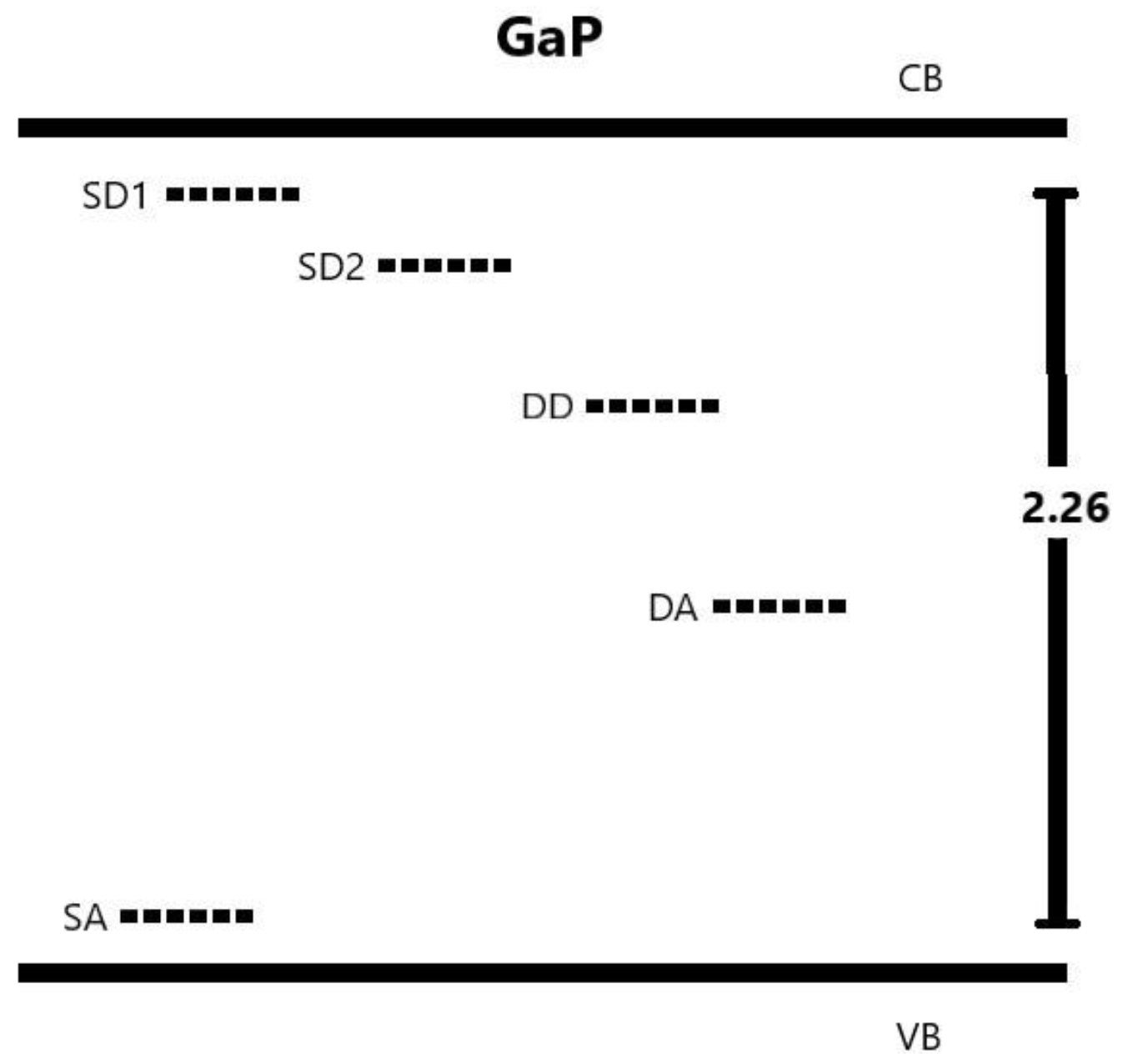
Figure 1. The energy model of the material structure adopted during the simulation. The designations CB and VB denote the conductivity and valence bands, respectively. The defect symbols SD1, SD2, DD, DA, and SA denote in order two shallow donor defects, one deep donor, one deep acceptor, and one shallow acceptor.
Energies 16 01725 g001
Figure 2. Simulation of the dependence of the resistivity of an unlit material on the concentration of the defect SD1, SD2, DD, DA, and SA defect concentration equal to 1.3 × 10¹⁴, 3.4 × 10¹⁴, 3.3 × 10¹⁵, and 2.8 × 1014 cm−3, respectively. Simulations carried out at the temperature of 300 K.
Energies 16 01725 g002
Figure 3. Illustration of the peak photocurrent values depending on the value of the coefficient of generation of electron-hole pairs G. The simulation values were assigned to the experimental values depending on the carrier lifetime coefficient τ. Simulations carried out for a temperature of 300 K.
Energies 16 01725 g003
Figure 4. Changes in material resistivity over time for the generation coefficient values corresponding to the results of experimental tests of the GaP-1 sample. The inset shows an approximation of the first 400 ns. At time zero, the lighting of the sample is turned on. Measurements carried out at a temperature of 300 K.
Energies 16 01725 g004
Figure 5. Changes in the concentration of electrons in the conduction band over time for the value of the generation coefficient corresponding to the results of experimental tests of the GaP-1 sample. The y-axis is presented on a logarithmic scale. The inset shows an approximation of the first 300 ns. At time zero, the lighting of the sample is turned on. Measurements carried out at a temperature of 300 K.
Energies 16 01725 g005
Figure 6. Changes in the concentration of holes in the valence band over time for the value of the generation coefficient corresponding to the results of experimental studies of the GaP-1 sample. The inset shows an approximation of the first 400 ns. At time zero, the lighting of the sample is turned on. Measurements carried out at a temperature of 300 K.
Energies 16 01725 g006
Table 1. Assumed parameters of the defect centers for the simulated material.
SymbolDefect TypeActivation Energy (eV)Capture Cross-Section (cm2)Identification
ElectronsHoles
SD1shallow donor0.0851.95 × 10−15-SiGa0 [23,24]
SD2shallow donor0.1106.23 × 10−16-SP [23,24]
DDdeep donor1.0351.25 × 10−14-PGa [23]
DAdeep acceptor0.850-7.04 × 10⁻¹⁵Unidentified [23]
SAshallow acceptor0.055-1.44 × 10⁻¹⁶CP [23,24]
Table 2. Parameters of the coefficients adopted to solve the kinetics equations.
SymbolConcentration (cm−3)Thermal Emission (s−1)Capture (cm3s−1)
ElectronsHolesElectronsHoles
SD10.8 × 10141.6837 × 1011-3.900 × 10⁻⁷-
SD21.3 × 10142.0452 × 109-1.246 × 10⁻⁸-
DD3.4 × 10141.1852 × 10−5-2.500 × 10⁻⁷-
DA3.3 × 1015-0.0090-9.152 × 10⁻⁸
SA2.8 × 1014-4.1688 × 10⁹-1.872 × 10⁻⁹
Table 3. The experimental and assigned simulation results for sample GaP-1.
Experimental ResultsSimulation Results
Photocurrent
(mA)
G Coefficient
(cm−3s−1)
τ (s−1)ρmin (Ωm)on (ns)off (ns)
0.4911.480 × 102028.11 × 10−9570665150
0.5092.565 × 102016.08 × 10−9549678220
0.5394.736 × 10208.64 × 10−95205175400
0.5526.018 × 10206.76 × 10−95087270700
Disclaimer/Publisher’s Note: The statements, opinions and data contained in all publications are solely those of the individual author(s) and contributor(s) and not of MDPI and/or the editor(s). MDPI and/or the editor(s) disclaim responsibility for any injury to people or property resulting from any ideas, methods, instructions or products referred to in the content.