Article

Modeling and Experimental Validation of a Voltage-Controlled Split-Pi Converter Interfacing a High-Voltage ESS with a DC Microgrid

by
Massimiliano Luna
1,
Antonino Sferlazza
2,*,
Angelo Accetta
1,
Maria Carmela Di Piazza
1,
Giuseppe La Tona
1 and
Marcello Pucci
1
1
Consiglio Nazionale delle Ricerche (CNR), Istituto di Ingegneria del Mare (INM), Via Ugo La Malfa 153, 90146 Palermo, Italy
2
Dipartimento di Ingegneria (DI), Università degli Studi di Palermo, Viale delle Scienze ed. 10, 90128 Palermo, Italy
*
Author to whom correspondence should be addressed.
Energies 2023, 16(4), 1612; https://doi.org/10.3390/en16041612
Submission received: 30 December 2022 / Revised: 31 January 2023 / Accepted: 2 February 2023 / Published: 6 February 2023

Abstract

:
The Split-pi converter can suitably interface an energy storage system (ESS) with a DC microgrid when galvanic isolation is not needed. Usually, the ESS voltage is lower than the grid-side voltage. However, limitations in terms of the ESS current make the use of a high-voltage ESS unavoidable when high power levels are required. In such cases, the ESS voltage can be higher than the microgrid voltage, especially with low microgrid voltages such as 48 V. Despite its bidirectionality and symmetry, the Split-pi exhibits a completely different dynamic behavior if its input and output ports are exchanged. Thus, the present work aims to model the Split-pi converter operating with an ESS voltage higher than the grid-side voltage in three typical microgrid scenarios where the controlled variable is the converter’s output voltage. The devised state-space model considers the parasitic elements and the correct load model for each scenario. Furthermore, it is shown that the presence of the input LC filter can make the design of the loop controllers more complicated than in the case of a lower ESS voltage than the grid-side voltage. Finally, the study is validated through simulations and experimental tests on a lab prototype, and a robustness analysis is performed.

1. Introduction

The growing interest in DC electrical microgrids has triggered a renewed interest in power electronics, specifically in the devices and circuits enabling the correct interfacing of a DC bus with distributed generation units, energy storage systems (ESSs), and passive or active loads. In particular, bidirectional DC/DC converters used to interface ESSs with DC buses are considered crucial due to the manifold beneficial effects of ESSs on DC microgrids [1,2]. In fact, ESSs play a key role in providing the needed flexibility to maintain the stable operation of the microgrid. Furthermore, they improve the system’s robustness and resiliency by compensating for the intermittency of renewable generation, providing ramping support to generators, and acting as backup power sources. Finally, ESSs ensure a power buffer that can be leveraged to apply suitable energy management strategies to the microgrids by defining the optimal power flows according to the chosen objectives [3,4,5]. For example, the minimum electricity bill, the maximum efficiency, or the minimum load demand uncertainty can be pursued. In addition, bidirectional DC/DC converters are also increasingly employed in other applications, such as uninterruptable power supplies and electric vehicles [6].
The simplest bidirectional DC/DC converters are non-isolated and are obtained by replacing the unidirectional switches of the basic DC/DC converter topologies with bidirectional switches. Additional degrees of freedom can be achieved with isolated topologies based on high-frequency transformers (HFTs), where the turn ratio of the HFT can be used to adjust the boosting capability of the converter. In such structures, the galvanic isolation between the input and output ports of the converter provides the circuit with increased safety. The most popular isolated bidirectional DC/DC converter is the Dual Active Bridge (DAB) converter [7,8]. It is based on two full-bridge circuits, each of which is placed on one side of the HFT. This converter is particularly suited to high-power applications. Recent studies also put in evidence the good attitude of the DAB in providing an active current limitation in case of a short circuit at the output terminals. This capability is of the utmost importance in DC microgrids, where the design of an appropriate protection system remains a significant challenge so far [7,8].
Most of the current research on circuit topologies for bidirectional DC/DC converters is focused on minimizing weight, volume, losses, and cost and on enhancing power density and reliability using wide-bandgap (WBG) semiconductors. In addition, recent research has mainly focused on topologies that are inherently scalable and modular [9]. From this point of view, non-isolated bidirectional DC/DC converters are interesting since they can provide benefits in terms of efficiency, size, weight, cost, and modularity [5,7].
Reference [7] presents an exhaustive overview of DC/DC bidirectional converters. Besides reviewing both non-isolated and isolated configurations, the most relevant control schemes and switching strategies were analyzed for both converter categories. The need for designing highly efficient and reliable soft-switching strategies was highlighted. Furthermore, whenever applicable, the combination of pulse width modulation (PWM) with single-phase shift control was suggested to limit current stress, circulating currents, and conduction losses. Such a combination can also expand the range of the zero-voltage switching (ZVS) operation.
In [9], a comparative analysis was conducted to assess the suitability of several single-phase non-isolated bidirectional DC/DC converters to be used in DC microgrids with multiple ESSs. The study focused on power sharing among distributed generation units by using droop control to equalize the state of charge (SOC) of multiple ESS architectures in both charging and discharging modes. Several topologies (e.g., single-stage and cascaded buck-boost, buck-boost with tapped inductors, and SEPIC) were investigated and compared in terms of DC voltage regulation, discharge current, SOC discharge rate, and number of active/passive circuit components. In addition, extensive reviews of non-isolated bidirectional DC/DC converter structures were presented in [5,10]. The studies included converter classifications based on efficiency, simplicity, cost, and flexibility. Moreover, the half-bridge topology with coupled inductors (including the related interleaved variants) was identified as the most promising topology from the efficiency and robustness standpoints.
Among the non-isolated bidirectional DC/DC converters, the Split-pi recently emerged as a noteworthy option. This converter is based on two cascaded half-bridge converters (HBCs) with a common bulk capacitor, as shown in Figure 1. It can work in four operating modes, which depend on the relationship between the voltage at the input and output ports and the power flow direction, according to Table 1. As a matter of fact, there are not many papers on the Split-pi available in the literature [11,12,13,14,15,16,17,18,19,20,21,22,23,24]. In particular, refs. [11,12,13,14,15,16,17,18] analyzed various aspects of the Split-pi topology and its open-loop control, showing that this converter features high efficiency like the DAB but also exhibits reduced switch count, smaller reactive components, and suitability for multiphase systems.
On the other hand, only six papers studied the performance of the Split-pi under a closed-loop control [19,20,21,22,23,24]. In particular, ref. [19] focused on the regulation of the internal bulk capacitor’s voltage and [20,21] regulated the output voltage of the converter connected to a passive load, whereas [22] controlled the power flow in a Split-pi connected to a microgrid with stiff voltage regulation.
A more extensive study was performed in [23,24] to show how to correctly model and control the Split-pi used as an ESS converter operating in Modes 1 and 2 in all the five possible DC microgrid scenarios. Such scenarios stem from the combination of the nature of the active load of the ESS converter and the three possible control modes for the converter itself. On the one hand, the ESS converter can be controlled to behave either as a non-stiff voltage generator, a stiff voltage generator, or a current generator under the supervision of an energy management system (EMS). On the other hand, the DC microgrid can or cannot encompass droop-controlled voltage generators in addition to current generators and passive loads.
Although [23,24] considered the Split-pi operating in Modes 1 and 2, the operation in Modes 3 and 4 (i.e., with ESS voltage higher than grid-side voltage) is also possible. For example, using a high-voltage ESS (i.e., above 200 V) is unavoidable when high power levels are required because of the limitations in terms of the ESS current that arise from technical and safety considerations. In such a case, the ESS voltage can be higher than the microgrid voltage, especially with low microgrid voltages such as 48 V.
Given the bidirectional and symmetrical nature of the Split-pi, in the first place, it could seem that exchanging the relationship between the voltages of the ESS and the DC bus (i.e., considering Modes 3–4 instead of Modes 1–2) does not imply any modification with respect to the configuration studied in [23]. Instead, as will be shown in Section 2, the Split-pi converter exhibits a different dynamic behavior if its input and output ports are exchanged. This result is counter-intuitive considering the bidirectionality and symmetry of the converter, and it implies a more complicated design of the converter controllers and a more limited bandwidth. Thus, it is worth being investigated in detail.
The present work considers the same Split-pi converter as in [23,24]. However, the voltage levels of the ESS and the DC microgrid are exchanged, i.e., the Split-pi is supposed to interface a 180 V, 750 W storage system with a 48 V DC microgrid. Thus, the converter is operated in Modes 3–4. The study is performed in three of the five possible DC microgrid scenarios, i.e., those in which the controlled variable is the converter’s output voltage rather than the output current. A state-space model of the converter is devised considering the parasitic elements and the correct load model for each scenario. The study is validated performing simulations and experimental tests on the same prototypal Split-pi described in [24]. The obtained experimental results are coherent with the simulations and validate the study. Finally, a robustness analysis is performed, and the limitations of the proposed converter are discussed.
The paper is structured as follows. Section 2 clearly highlights the differences between the operation in Modes 1–2 vs. Modes 3–4 and recalls the case study, the DC microgrid scenarios, and the closed-loop control scheme. Section 3 describes the state-space model of the Split-pi operating with an ESS voltage higher than the grid-side voltage and the design of the control system. The simulations and experimental tests are described and commented on in Section 4 and Section 5, respectively. Section 6 presents a robustness analysis and discusses the limitations of the proposed converter. Finally, some conclusions are drawn.

2. Comparison between Operation in Modes 1–2 vs. Modes 3–4 and Overview of Previous Work

In this section, the differences between the Split-pi operation used as a storage converter with the ESS voltage lower or higher than the grid-side voltage are clearly highlighted. Then, the case study, the possible DC microgrid scenarios, and the closed-loop control scheme are briefly recalled from [23].

2.1. Comparison between Operation in Modes 1–2 vs. Modes 3–4

It is possible to refer to Figure 2 to understand the reason for the different behavior of the proposed storage converter in Modes 1–2 vs. Modes 3–4. Indeed, for power flowing from the high side to the low side (i.e., in Modes 2 and 3), the converter is characterized by the same topology: an LC filter followed by a buck converter. Such a filter is formed by the high-side inductor and the bulk capacitor. Likewise, for power flowing from the low side to the high side (i.e., in Modes 1 and 4), the Split-pi always behaves as a boost converter followed by an LC filter formed by the high-side inductor and the high-side capacitor.
However, further reasoning highlights a substantial difference that makes the storage converter’s state-space model different from the one devised in [23]. A perfect symmetry would imply also exchanging the controlled variables IL1 and V2 with IL2 and V1, respectively. In this condition, the state-space model would not change. However, this exchange is not possible since the goal for a storage converter is to control the output voltage (to perform grid voltage regulation) and the storage current (to keep it within the limits recommended by the manufacturer). As will be shown in Section 3, not exchanging the controlled variables results in a different state-space model of the converter.
Specifically, in Mode 1, the inner control loop regulates the boost converter’s input current, whereas the input current of the LC filter (formed with the high-side capacitor) is controlled in Mode 4. Likewise, in Mode 2, the inner control loop regulates the current on the inductor of the buck’s output filter (formed with the low-side capacitor). On the other hand, in Mode 3, the inner control loop regulates the current on the LC filter formed with the bulk capacitor located before the buck converter.
As will be shown in Section 3, if the resonance introduced by the latter filter is poorly damped, the design of the controllers becomes more complicated than in the case of the Split-pi operating in Modes 1–2, and a more limited bandwidth can be achieved.

2.2. Overview of the Case Study

The chosen case study is a Split-pi converter interfacing a 180 V, 750 W battery storage system with a 48 V DC microgrid encompassing passive and active loads. For example, it could represent a scaled version of the DC microgrid onboard an unmanned marine vehicle with several low-power 48 V loads whose combination exceeds the maximum operational current of a single 48 V battery. In such a case, it is worth connecting the required number of batteries in series to reduce the storage current and, thus, the cables’ volume and weight.
The switching frequency value was chosen as a compromise between the dynamic performance and losses. Then, the reactive components of the Split-pi were sized by limiting the maximum ripple on the inductor current (ri% = ±6.0%), the external capacitors’ voltage (rve% = ±0.2%), and the bulk capacitor (rv% = ±0.2%). Most of the rated parameters of the Split-pi chosen as a case study are the same as those reported in Table 3 of [23]. Nevertheless, some parameters were changed to allow the operation in Modes 3 and 4. In particular, the input and output currents/voltages are exchanged; the maximum ESS charge/discharge current is now 5 A; and the nominal duty cycle and load resistance are d ¯ = 0.277 and Rn = 3.333 Ω, respectively. Table 2 summarizes the main parameters of the Split-pi converter considered in the present study. Furthermore, it is worth highlighting that the duty cycles of the four switches in Modes 3 and 4 are {HBC1_top, HBC1_bottom, HBC2_top, HBC2_bottom} = {1, 0, d, 1 − d}.
As for the droop characteristics of the storage converter and the voltage generator of the microgrid, they were designed as follows. The droop parameters chosen for the ESS converter in Scenarios #2 and #3 were Eds = 50 V and Rds = 0.2 Ω. They were chosen to impose a 6% voltage reduction at the nominal current. On the other hand, the droop parameters of the microgrid’s voltage generator in Scenario #3 were Ed = 55 V and Rd = 0.666 Ω. With such values, the ESS was supposed to be inactive for 50% of the microgrid’s rated load power and charged below (or discharged above) such a threshold.

2.3. DC Microgrid Scenarios

Following the approach of [23], it is possible to consider five DC microgrid scenarios. They stem from the valid combinations of the three control modes that can be used for the power converters of the microgrid devices: non-stiff droop control, stiff droop control, and current control. Such scenarios are summarized in Table 3, which is a more compact version of the table reported in [23]. For improved clarity, each scenario is also referred to using an abbreviation like Sx–Gy, where x and y denote the control mode for the storage (S) and grid-side (G) converters. For example, D = non-stiff droop control; S = stiff droop control; C = current control; and N = no grid-side generator is present or operated in droop mode. In the present work, only the first three scenarios are analyzed, i.e., those in which the controlled variable is the Split-pi’s output voltage.
In general, the load of the ESS converter is the combination of the voltage/current microgrid generators and passive loads. If droop-controlled voltage generators are present, they can be aggregated into a single equivalent generator with no-load voltage Ed and droop resistance Rd. Current generators can be aggregated into a single generator I. Ultimately, in the first three scenarios, the converter’s load can be easily reduced to an equivalent load resistor R parallel connected to a current generator Ieq, as shown in [23].

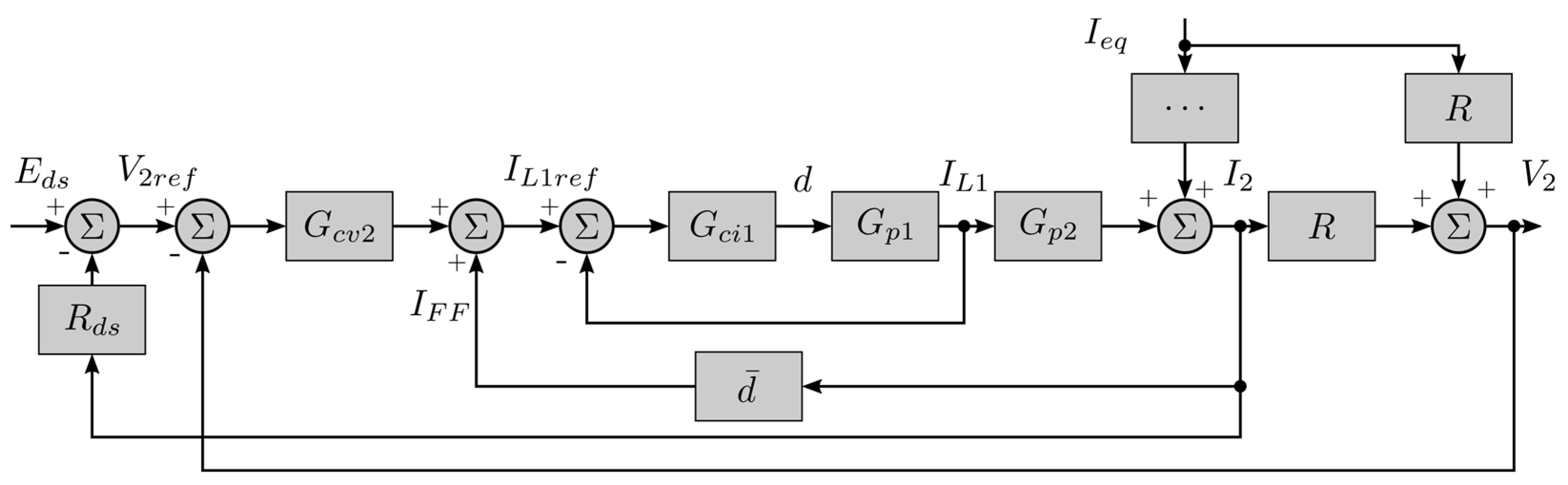
2.4. Closed-Loop Control Scheme

The closed-loop control scheme for the ESS converter encompasses a current loop for IL1 and a voltage loop for V2 to control the storage-side current and the output voltage, respectively. The voltage loop is complemented by a feed-forward (FF) action to reduce the voltage overshoot. In Modes 3 and 4, the FF term is the nominal duty cycle d ¯ , whereas it is (1 − d ¯ )−1 in Modes 1 and 2. Furthermore, in Scenarios #2 and #3, a third loop is required to implement the storage converter’s droop characteristic. In order to prove the merit of the FF action, it is worth considering also a baseline scenario derived from Scenario #1 by deactivating the FF action.
The complete closed-loop control scheme is shown in Figure 3. In such a scheme, Gp1(s) is the transfer function that expresses the relationship between d and IL1; Gp2(s) describes the dependence of the output current I2 on IL1; and Gp2(s)·R expresses the relationship between IL1 and V2. The transfer functions of the current and voltage controllers are denoted by Gci1(s) and Gcv2(s). The external current generator Ieq behaves as a disturbance that is suitably compensated for by the control system, regardless of its transfer function.
As in the usual practice, the duty cycle was limited between 0 and 0.95 to avoid prolonged transients with a unity duty cycle, which corresponds to a short circuit for the source of the HBC that works as a boost converter. This limitation did not affect the control performance since the duty cycle had an average value d ¯  = 0.277 and never reached 0.95, not even during transients, as will be shown in Section 4 and Section 5. Furthermore, the reference for the inductor current IL1 was saturated to comply with the maximum charging/discharging current of the ESS and the allowed SOC limits. This limitation slightly reduced the dynamic performance of the system but was required to guarantee a safe operation of the ESS.

3. State-Space Model and Control System Design

In this section, the state-space model of the Split-pi converter operating in Modes 3–4 in Scenarios #1–#3 is given. Furthermore, based on such a model, the control system design procedure is described, and the parameters of the designed controllers are given for each scenario.

3.1. State-Space Model

The state-space model of the voltage-controlled Split-pi operating with an ESS voltage higher than the grid-side voltage was determined according to [25], considering the parasitic elements. It can be expressed in matrix form as follows:
{ x ˙ = A x + B u y = C x + D u   with   { A = d A o n + ( 1 d ) A o f f B = d B o n + ( 1 d ) B o f f C = d A o n + ( 1 d ) C o f f D = d D o n + ( 1 d ) D o f f
by considering Rp = R//Re, Rsum = R + Re, Rtot = Rp + RL + Rc, and:
x = [ I L 1 ,   I L 2 ,   V c ,   V e ]
u = [ V 1 , I e q ]       y = [ I L 1 , V 2 , I 2 ]
A o n = [ R L + R c L R c L 1 L 0 R c L R t o t L 1 L R L R s u m 1 C 1 C 0 0 0 R R s u m C e 0 1 R s u m C e ]
A o f f = [ R L + R c L 0 1 L 0 0 R p + R L L 0 R L R s u m 1 C 0 0 0 0 R R s u m C e 0 1 R s u m C e ]  
B o n = B o f f = [ 1 L 0 0 R p L 0 0 0 R R s u m C e ]
C o n = C o f f = [ 1 0 0 0 0 R p 0 R R s u m 0 R e R s u m 0 1 R s u m ]
D o n = D o f f = [ 0 0 0 R p 0 R R s u m ]
It can be noticed that the matrices Aon and Aoff of the model are different from those devised in [23] for a Split-pi operating in Modes 1–2. This results in different system dynamics.

3.2. Control System Design

By leveraging the devised model, it is possible to design a suitable control system for the Split-pi converter. In this work, classic PI or PID controllers were considered according to the approach shown in [26]. Thus, the general transfer function expressed by (9) was considered.
G P I D ( s ) = ( K p + K i s + s K d ) 1 1 + s K d N K p
where N is typically chosen greater than 10.
In order to design the PID controller, the state-space model was linearized around the rated operating point corresponding to d ¯ and x ¯ = [ I L 10 ,   I L 20 ,   V c 0 ,   V e 0 ] = [ 4.167 ,   15 ,   180 ,   50 ] , thus obtaining the small-signal transfer functions G p 1 ( s ) and G p 2 ( s ) . Then, the controllers G c i 1 ( s ) and G c v 2 ( s ) were designed based on the Bode diagrams of the two open-loop subsystems. More precisely, the controllers G c i 1 ( s ) and G c v 2 ( s ) were designed to impose suitable values of the crossover frequency ω c and phase margin m φ and to ensure a suitable gain margin mg [23,27]. Such specifications ( ω c , m φ , and mg) were evaluated considering the open-loop function G F i ( s ) = G c i 1 ( s ) G p 1 ( s ) for the inner loop and the function G F v ( s ) = G c v 2 ( s ) G c i 1 ( s ) G p 1 ( s )   1 + G c i 1 ( s ) G p 1 ( s )   for the outer loop. To impose suitable values of the crossover frequency ω c and phase margin m φ , the controller parameters K p , K i , and K d of the PID were chosen such that the following equations were satisfied:
| G c ( j ω c ) | | G p ( j ω c ) | = 1
a r g ( G c ( j ω c ) ) + a r g ( G p ( j ω c ) ) + 180 ° = m φ
In such equations, G c ( · ) and G p ( · ) are either G c i 1 ( · ) and G p 1 ( · )  if the inner loop is considered or G c v 2 ( · ) and G c i 1 ( · ) G p 1 ( · )   1 + G c i 1 ( · ) G p 1 ( · )   if the outer loop is considered. Equations (10) and (11) can be solved analytically. Subsequently, by means of the Bode diagrams of G F i ( s ) and G F v ( s ) , it is verified that the gain margin is sufficiently high, typically higher than 12 dB.
Note that the crossover frequency influences the dynamic performance of the closed-loop system. In general, it must be as high as possible but at least 10 times lower than the switching frequency so that the controller does not process the switching ripple. Furthermore, for proper decoupling between the voltage and current loops, the crossover frequency of the external loop must be suitably lower than that of the internal loop. The phase and gain margins characterize the stability of the closed-loop system and affect the damping of the system response. A phase margin of 50°–60° is usually enough in the case of passive loads. Instead, active loads require a higher phase margin than 85° to ensure stability under every possible operating condition. Finally, to guarantee stability despite parameter variations, a gain margin higher than 12 dB is required for both passive and active loads.
Although the state-space model was linearized around the rated operating point, i.e., considering the rated load resistance R, the designed controllers are supposed to also perform well with lower loads thanks to their wide stability margins. It is also worth noting that it was R = Rn in Scenarios baseline, #1 and #2. On the other hand, in Scenario #3, R was very low because it resulted from the parallel connection of Rn and the droop resistance Rd of the voltage generator.
The parameters of the designed controllers are summarized in Table 4. Some noteworthy remarks can be made about the controller design for Modes 3–4. The LC filter before HBC1 determined a resonance at ω = 1330 rad/s with very low damping (ζ = 0.1). If the related complex conjugate poles were not canceled, the achievable bandwidth was quite limited. Therefore, a PI regulator was unsuitable and, thus, a PID regulator was needed. The phase margin that resulted after satisfying all the design constraints was slightly higher than 85°, and the achievable crossover frequency could not exceed 1200 rad/s. In addition, a far pole at 105 rad/s should have been introduced in the current controller to decrease the gain at the switching frequency (Fsw = 20 kHz). However, the controller was to be implemented in discrete form with a sampling frequency equal to Fsw. Thus, the previously mentioned far pole could not be implemented and had to be moved down to 4·104 rad/s.
The current controller was in charge of compensating for the resonance only in the case of variations of current reference. Thus, load resistance variations had to be managed by the voltage controller alone. Such a controller was implemented as a PI regulator plus a pole at half the resonance frequency. Furthermore, the phase margin that resulted after satisfying all the design constraints was considerably higher than 85° to properly compensate for the resonance.
Referring to Table 4, all the scenarios exhibited nearly the same dynamics for IL1, so the related controllers had similar coefficients. As for the voltage controller, the sensitivity of the output voltage dynamics to R was high without the FF action. On the other hand, the FF action mitigated this sensitivity. Thus, similar voltage controllers were obtained in Scenarios #1, #2, and #3 despite the different values of R.

4. Simulation Results

Several simulations were performed to test the controlled system in the considered scenarios. The circuit model of the Split-pi was realized with PLECS (blockset version) based on Figure 1 and Table 1. The default parameters were confirmed for PLECS. On the other hand, the control system was implemented in Simulink according to Figure 3 and Table 4. All the default parameters were confirmed in the Simulink environment, except for the following:
  • Solver type: variable-step
  • Solver: ode23tb (stiff/TR-BDF2)
  • Max step size: 1/(10·Fsw)
  • Solver reset method: robust.
The obtained simulation results are presented and commented on in the following.

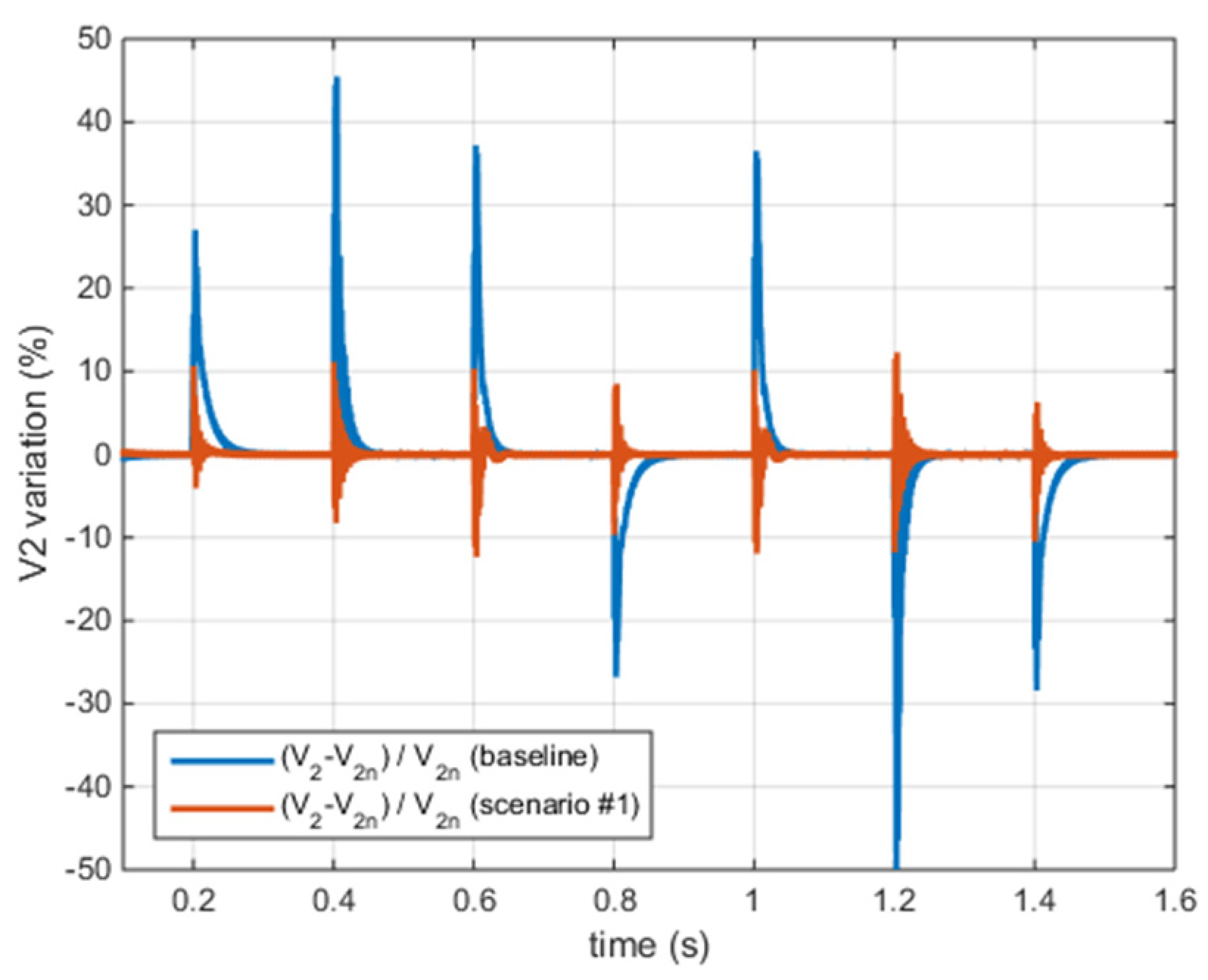
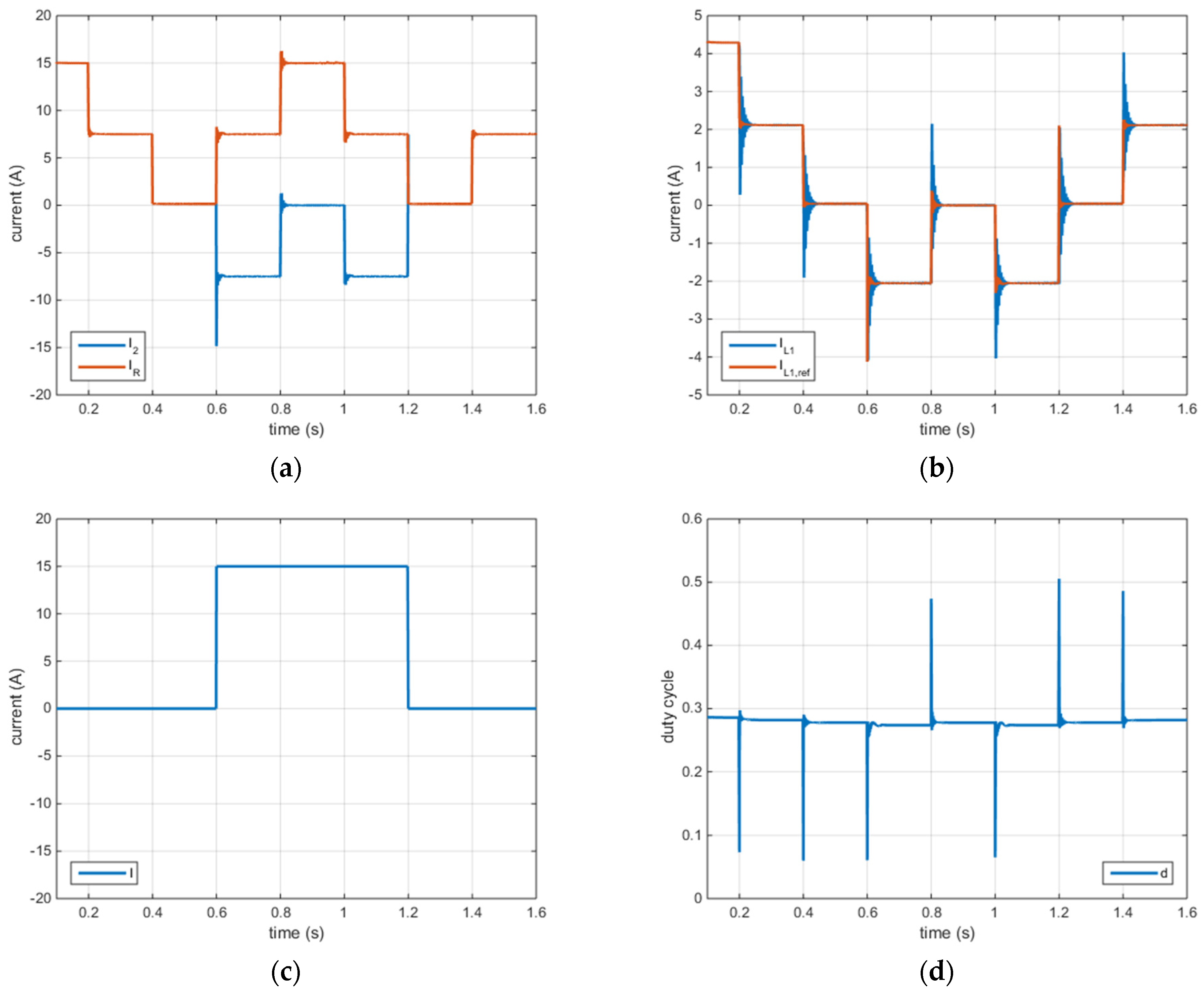
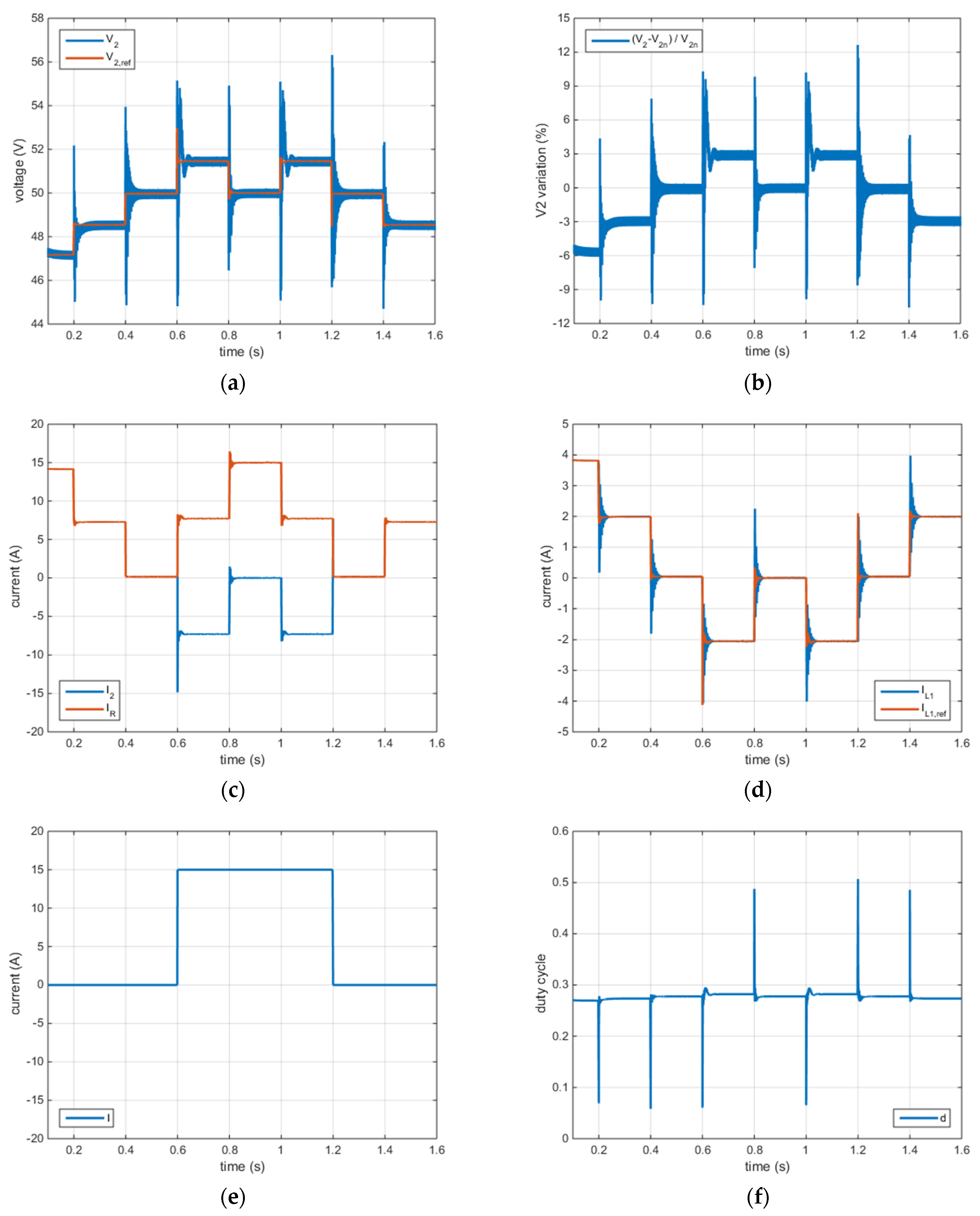
4.1. Baseline Scenario and Scenario #1 (SS-GN)

In the baseline scenario, the storage converter was used to regulate the microgrid voltage at 50 V and supply a passive load alone or with the help of an external current generator I. Furthermore, the FF action was deactivated. Before t = 0.2 s, the converter exhibited a steady-state output with R = Rn and I = 0. Then, the values of R and I were changed every 200 ms in a stepwise fashion according to the following sequences: R = {2, 100, 2, 1, 2, 100, 2}·Rn and I = {0, 0, 1, 1, 1, 0, 0}·In. This way, the storage system was discharged, charged, and discharged again. The waveforms of the main electrical and control variables are shown in Figure 4 and Figure 5. At each load resistance variation, the control system recomputed the duty cycle so the inductor current quickly tracked its reference value, although with some ringing due to the resonance. The output current followed the load resistance variations and became negative when the external generator supplied excess current. The percent variation of grid voltage with respect to the nominal output voltage V2n is shown in blue in Figure 5 and shows null error at a steady state. However, during transients, the undershoots and overshoots exceeded the allowed transient tolerance of ±20% by a large margin. Thus, the microgrid would have been automatically de-energized by the protection devices.
The FF action significantly improved the system response in Scenario #1, for which the simulation results are shown in Figure 5 and Figure 6. The duty cycle was varied instantaneously by the FF action at each load variation. Consequently, the waveforms of I2 and IR were almost square waves, and the maximum percent grid voltage variation was reduced to 12.3%, as shown in orange in Figure 5.
However, in general, the very large stepwise load variations considered in [23,24], i.e., Rn ↔ 100·Rn, cannot be tolerated in Modes 3 and 4. For such variations, even without the external current generator, the maximum overshoot with the FF action would be +27.3%. The only way to tolerate such perturbations would be to increase the resonance frequency and the damping factor of the LC filter by changing the values of L and C. However, the current and voltage ripple would increase as well. In any case, it is worth highlighting that stepwise variations are ideal perturbations useful for theoretical studies and are never to be encountered in real-world applications. In fact, using the FF action, the microgrid voltage variation never exceeded ±20% in the experimental tests described in Section 5.

4.2. Scenario #2 (SD-GN)

The control scheme of Scenario #2 encompassed the FF action and a third outer loop to implement the droop characteristic besides the internal loops for IL1 and V2. The same initial conditions and load sequence as in Scenario #1 were considered. The obtained results are shown in Figure 7 in terms of output voltage and output and load currents, as well as control variables (i.e., input inductor current and duty cycle). As expected, in steady-state conditions, the converter’s output voltage V2 tracked the reference voltage V2,ref computed according to the droop characteristic. For example, the steady-state voltage variation was −6% when the storage system was discharged at the rated power and +3% when it was recharged at half power. Even considering the overshoots, the maximum absolute grid voltage variation was 12.7% at t = 1.2 s. This result implied that the microgrid voltage stayed within +9.7% of its rated value (+3%) and was obtained despite the ideal stepwise variations of load resistance.
Finally, the waveforms of the output currents and the control variables were similar to those obtained in Scenario #1 (SS-GN).

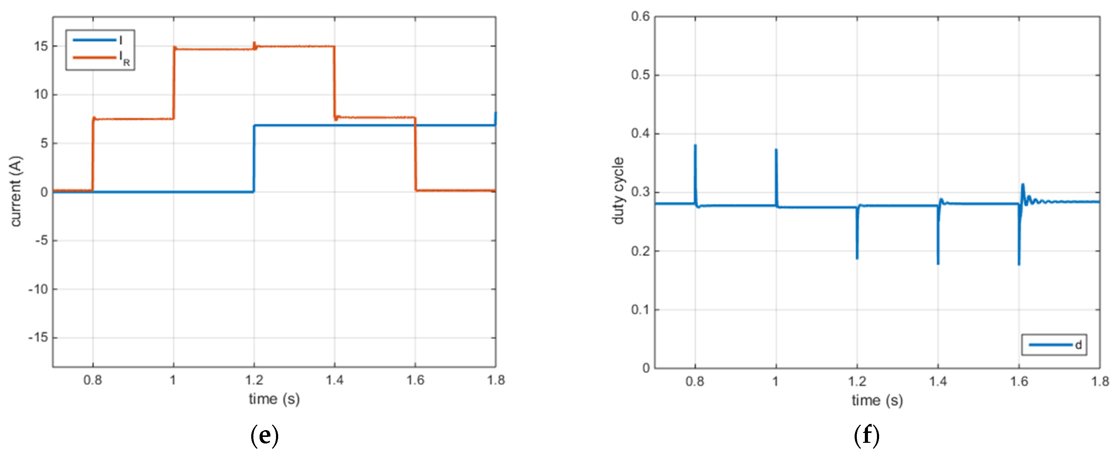
4.3. Scenario #3 (SD-GD)

The ESS converter and the voltage generator of the microgrid were both controlled in droop mode in Scenario #3. The two droop resistances were chosen so that the storage converter supplied no power for 50% of the microgrid’s rated load. Furthermore, a current generator I was also present in the microgrid. The waveforms of the most meaningful electrical and control quantities are shown in Figure 8. Before t = 0.8 s, the converter was in steady-state conditions with R = 100·Rn (low load) and I = 0. The ESS was recharged at Id = −5.65 A by the voltage generator, and the voltage variation was about +2%. Then, R and I were changed every 200 ms in a stepwise fashion according to the following sequences: R = {2, 1, 1, 2, 100}·Rn, I = {0, 0, 0.457, 0.457,0.457}·In. Thus, the current of the ESS converter exhibited the following values: 0 A, 5.5 A, 0 A, −5.15 A, and −10.8 A.
From Figure 8e, it is possible to evaluate the net current demand that had to be satisfied by the storage converter and the voltage generator of the microgrid. In particular, the net current was 50% of the rated value during the time intervals from t = 0.8 s to t = 1.0 s and from t = 1.2 s to t = 1.4 s. Thus, in such intervals, the current delivered by the storage converter was zero, as shown in Figure 8c, and the load was supplied only by the voltage generator. On the other hand, the battery was recharged/discharged when the net current demand was lower or higher than 50%, respectively.
The maximum absolute grid voltage variation exhibited during the test was 12.9%. Thus, it stayed well under 20%. The waveforms of the duty cycle and the input inductor current were close to those obtained in the former scenarios.

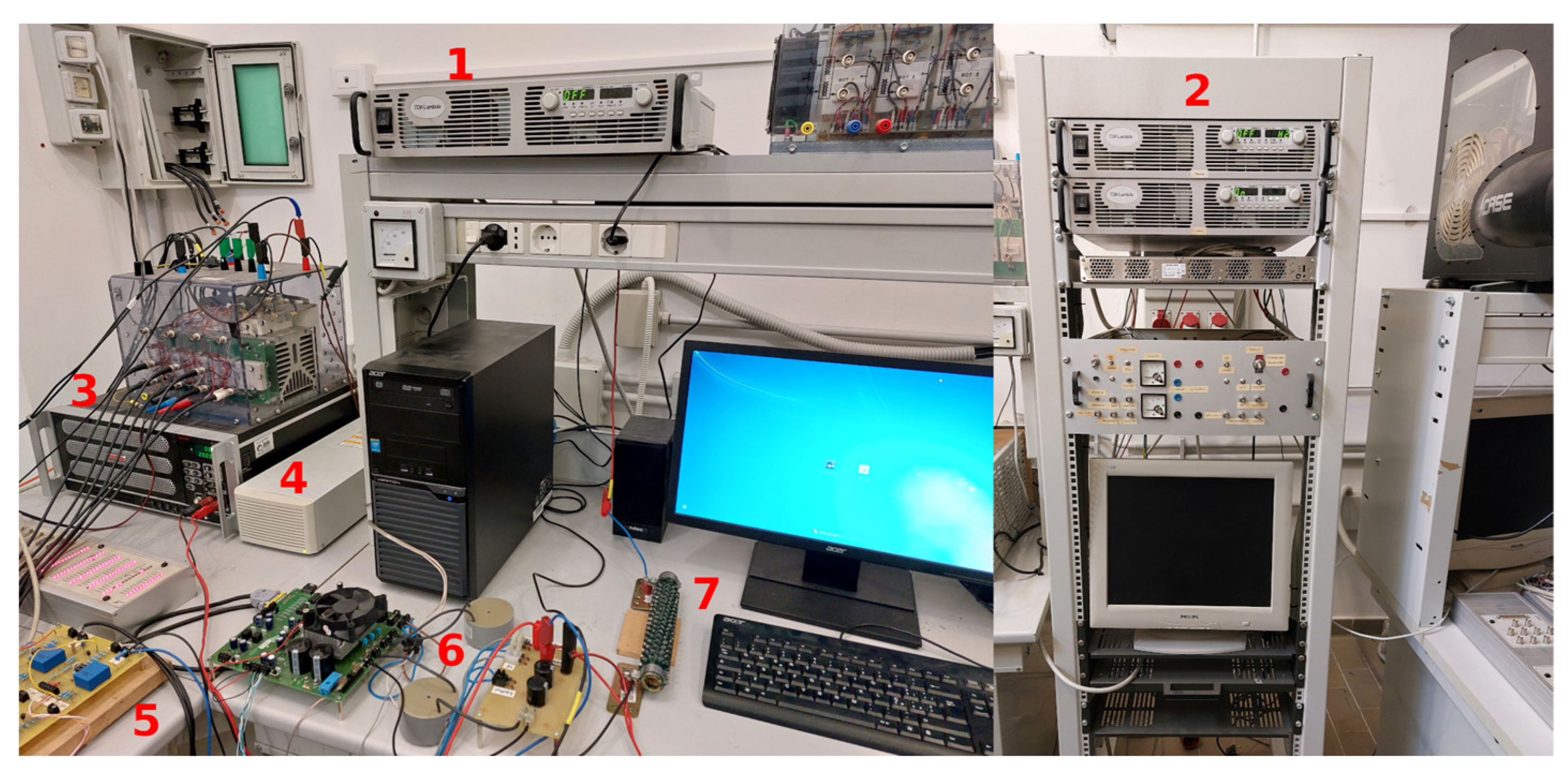
5. Experimental Validation

The details of the prototypal Split-pi converter and the related testbench were the same as in [24], but the input and output ports were exchanged. The converter prototype was based on an integrated power module STGIPS10K60A featuring a three-phase, IGBT-based H-bridge. The two inductors and the grid-side external capacitors were connected to the main board as external components. The storage system connected to the converter’s input was emulated using a TDK-Lambda GEN600-5.5 power supply set to 180 V. The active load connected to the converter’s output was composed of a Sorensen SLH-500-6-1800 programmable electronic load and a TDK-Lambda GEN60-40 power supply; the latter was used as a voltage generator or a current generator, depending on the scenario under test. In Scenario #3, a 1.2 Ω, 200 W power resistor was also used as the grid-side droop resistor. Figure 9 shows a photo of the whole experimental setup.
The electrical quantities of interest were measured using LEM-based voltage and current measurement circuits. They were acquired and saved by the dSPACE DS1103 board used to control the converter implementing the designed controllers and the PWM modulator. Later, they were imported into MATLAB and plotted. The obtained results are coherent with the simulation results and are discussed in the following subsections.

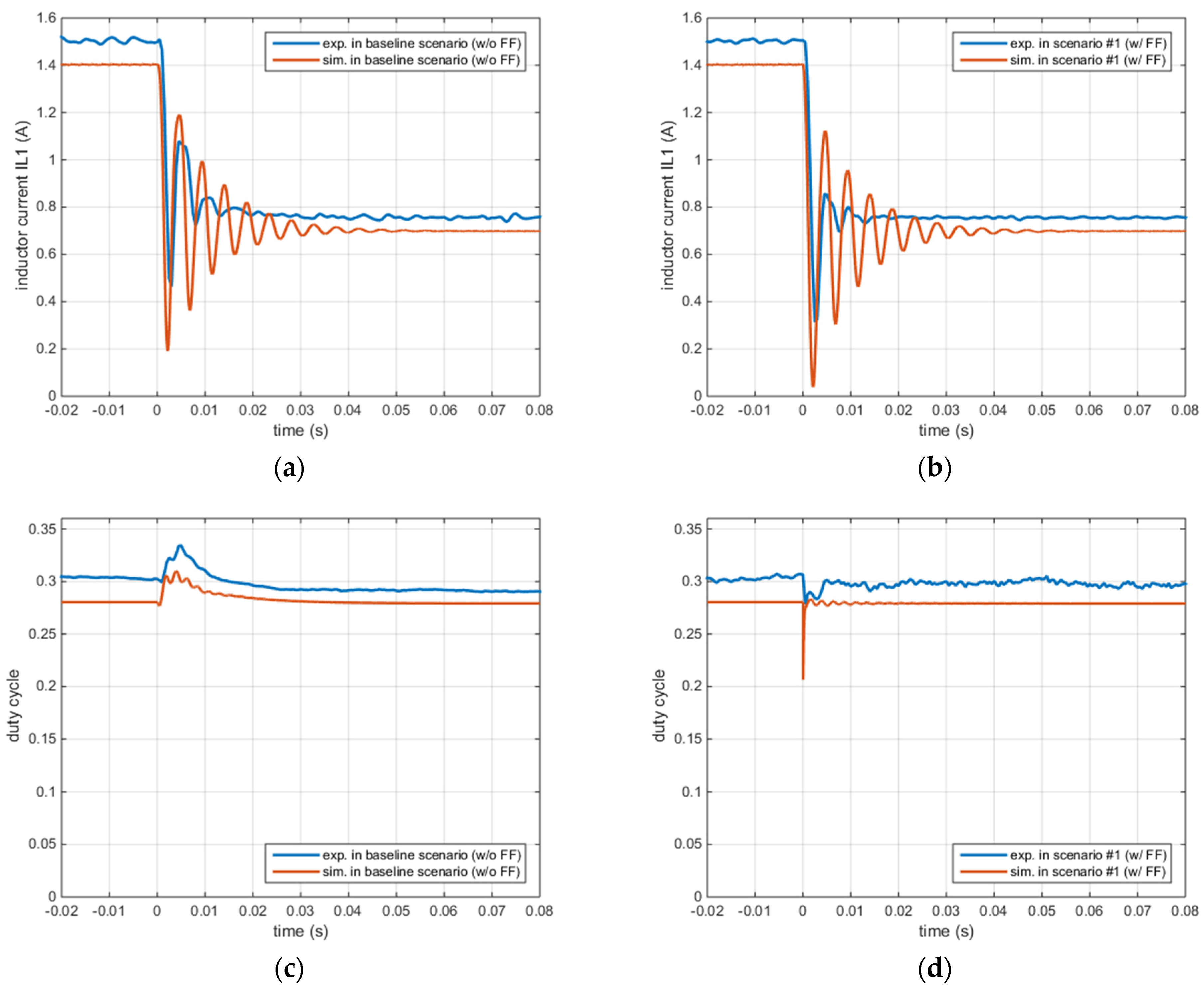
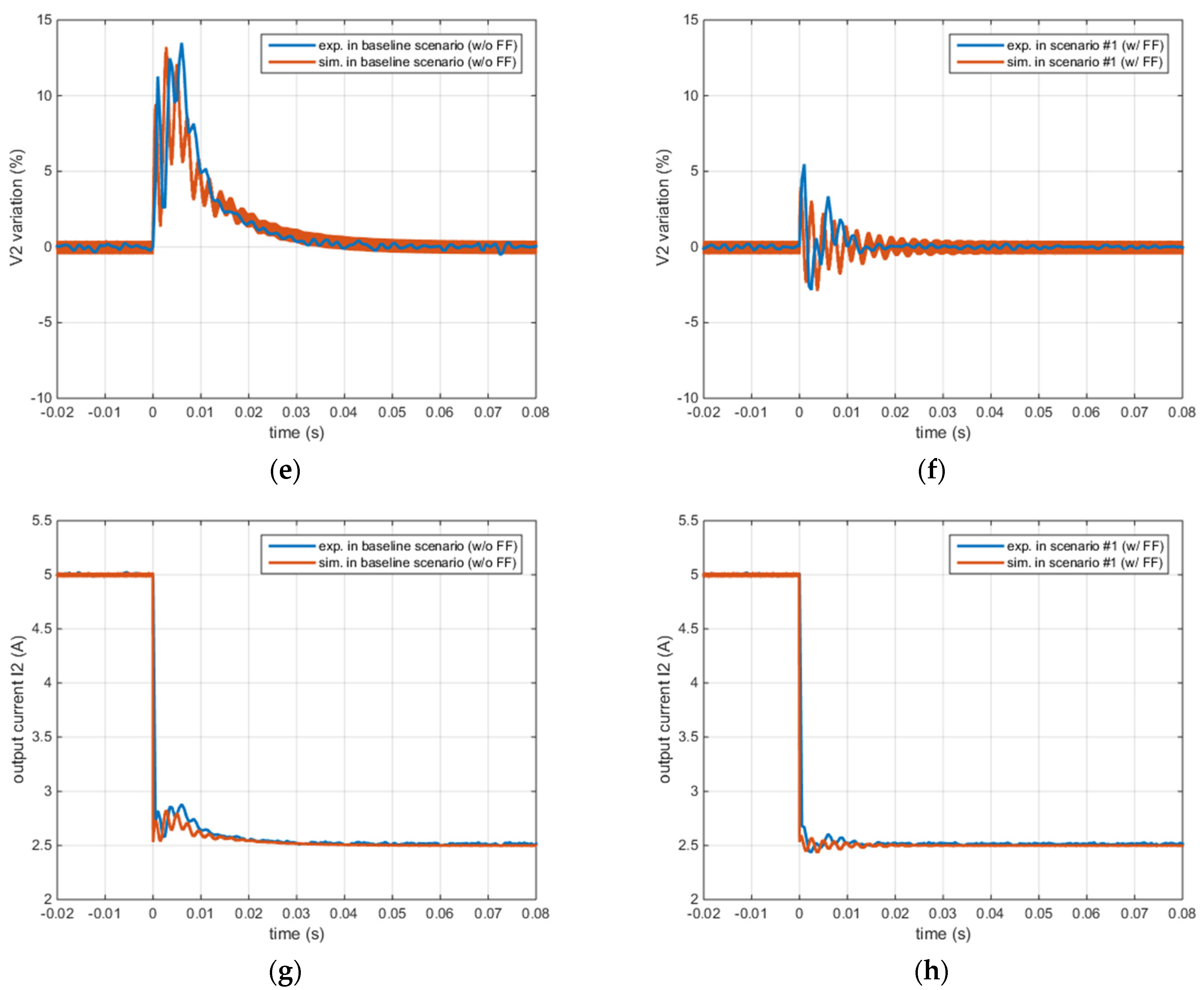
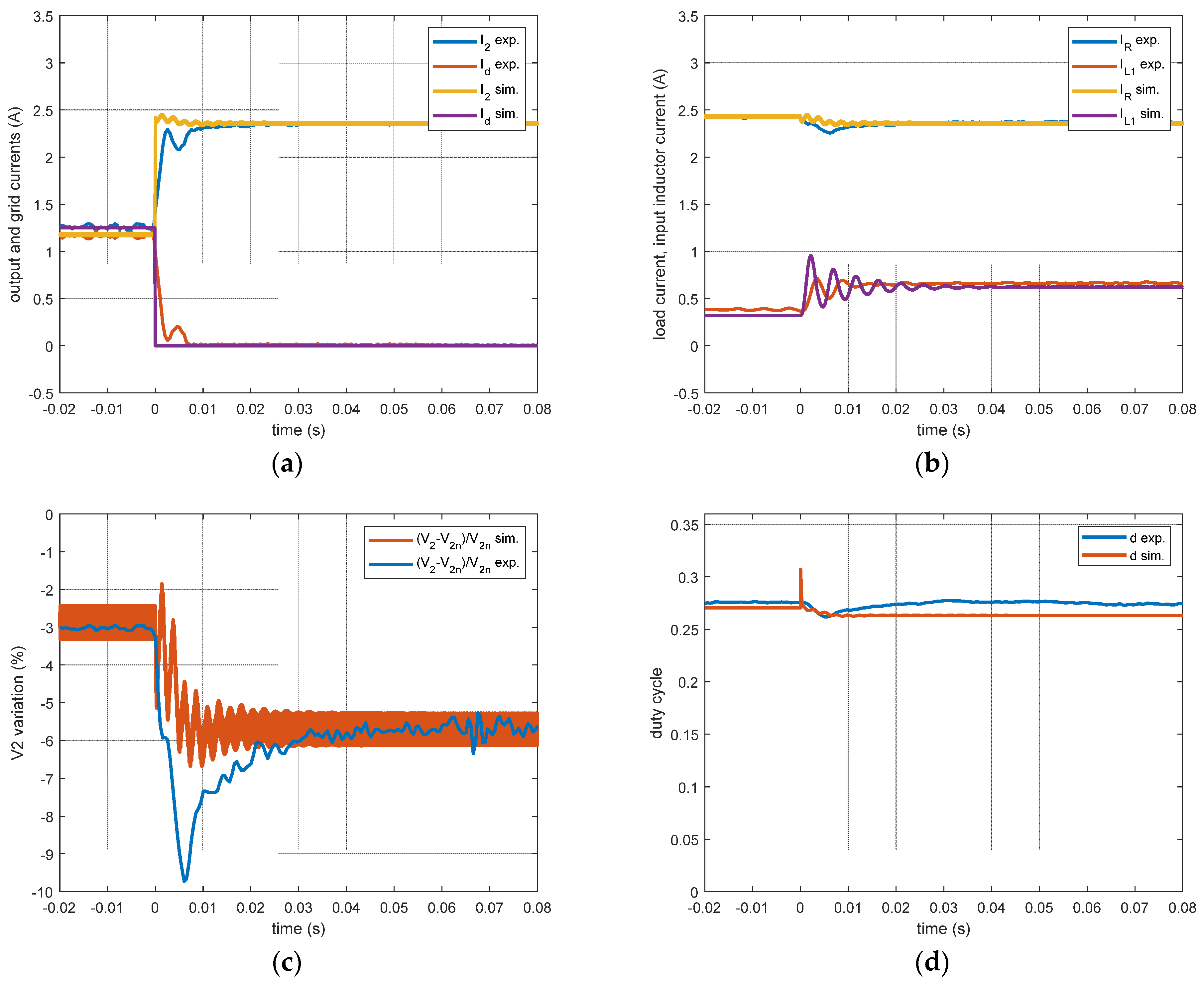
5.1. Baseline Scenario and Scenario #1 (SS-GN)

In these two tests, the Split-pi was used to form a stiff microgrid encompassing an aggregated passive load. The only difference between the two scenarios was the absence or presence of the FF action. The electronic load allowed applying a stepwise load variation from 10 Ω to 20 Ω at t = 0 s. As a result, the load power instantly decreased from 250 W to 125 W, causing a voltage overshoot on V2. The experimental results are presented in Figure 10 together with the simulation results. Each plot in Figure 10 shows that the simulation and experimental results were in good agreement. The vertical offset that is present in Figure 10a–d is due to the higher losses of the converter prototype compared to the simulation. Thus, the input current and the duty cycle had to be increased to obtain the desired output voltage. This behavior was expected because ideal semiconductor switches and diodes were considered in the simulations.
Furthermore, the comparison between the results obtained in the baseline scenario and in Scenario #1 confirmed that the FF action allowed for an instantaneous reduction of the duty cycle, which determined faster dynamics and reduced the voltage overshoot from 13.5% to 5.5%. Likewise, the undershoot on V2 was reduced from −11.2% to −5.6% for the opposite stepwise load variation. Even higher reductions are expected for larger variations of output power which, unfortunately, cannot be tested due to the limited power of the prototype.
Using the FF action, the output current waveform was pretty squared. Furthermore, the input inductor current showed faster dynamics and more limited ringing.

5.2. Scenario #2 (SD-GN)

In this test, the Split-pi converter formed a non-stiff microgrid characterized by a no-load voltage of 50 V and a droop resistance of 1.2 Ω. The active load was composed of a 20 Ω resistance and an external current generator Id set to 1.25 A. The latter was switched off at t = 0 s. The experimental results are shown in Figure 11 together with the simulation results. As the figure shows, before switching off the current generator, the storage converter delivered the remaining current quota needed to supply the load. Instead, when the current generator was switched off, the converter promptly supplied the entire load, as expected. According to the droop resistance value, the voltage variations with the current generator switched on and off were −3% and −5.66%, respectively. It is worth noting that the power supply was not able to impose an ideal current step. Thus, the experimental waveforms did not perfectly match the simulation results. Nonetheless, the control system instantly compensated for the actual current waveform produced by the external generator and succeeded in regulating the output voltage at the desired value.
Finally, the vertical offset in the waveforms of the input inductor current and the duty cycle was again due to the higher losses of the converter prototype compared to the simulations.

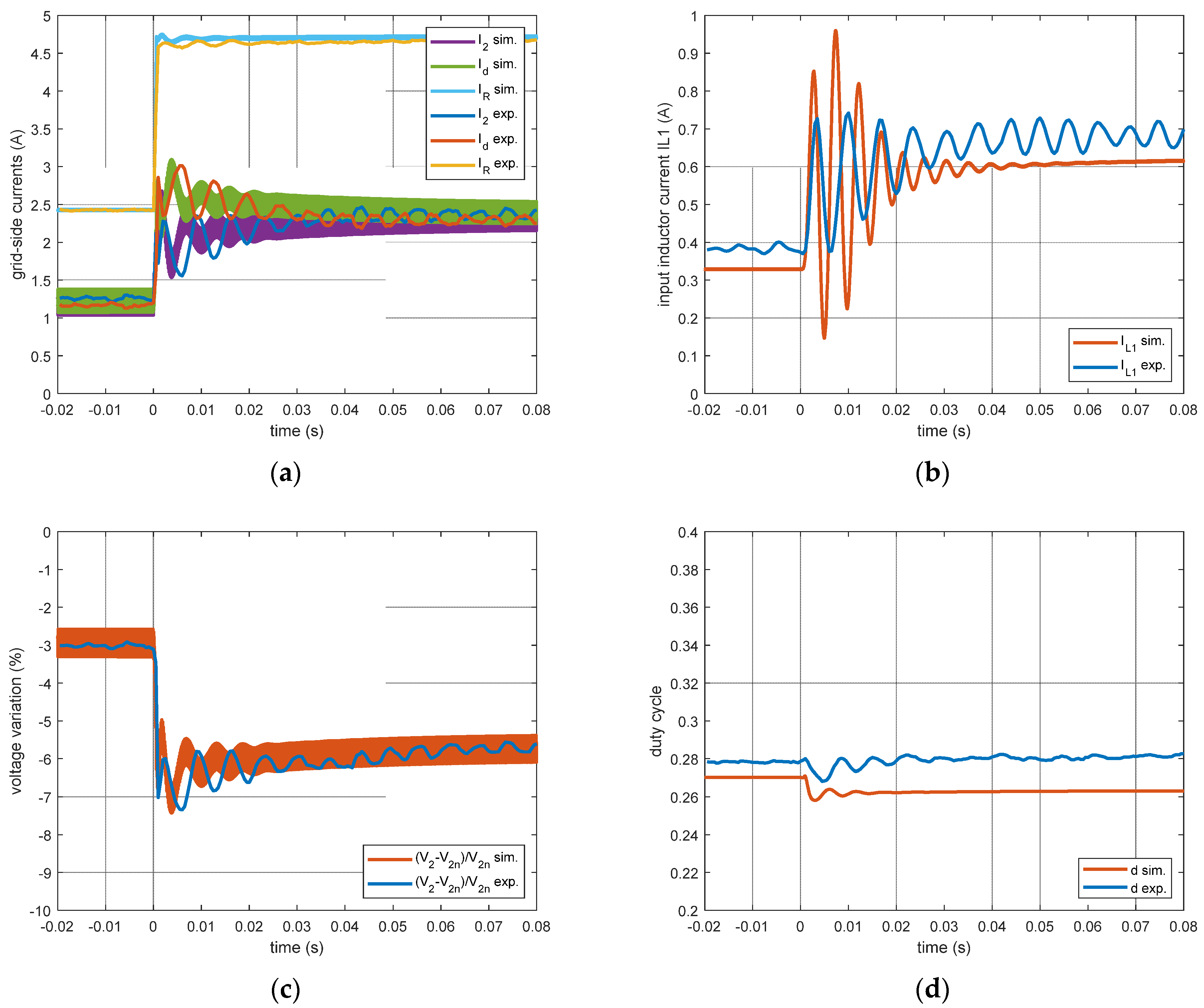
5.3. Scenario #3 (SD-GD)

During this test, the Split-pi converter and the microgrid voltage generator were controlled in droop mode with the same droop parameters (i.e., a droop resistance of 1.2 Ω and a no-load voltage of 50 V). Thus, the two devices were required to equally share the load for each value of the load resistance. The resulting microgrid was non-stiff. A stepwise variation of load resistance from 20 Ω to 10 Ω was applied at t = 0 s. The obtained waveforms are shown in Figure 12. As expected, the current sharing ratio was respected under steady-state conditions before and after the stepwise load-resistance variation.
Furthermore, the expected voltage variation was exhibited at each power level, i.e., −3% and −5.66%. Such values did not differ between Scenarios #2 and #3 because the two steady-state values of the converter’s output current in such scenarios were the same.
Finally, it is worth observing that the duty cycle variation was quite limited because the load was shared between the converter and the voltage generator of the microgrid.
By comparing the simulation and the experimental waveforms in Figure 12a,c, a good agreement can be noticed. The steady-state values and the slower time constant match. On the other hand, the ringing frequency of the experimental waveform was slower due to the unmodeled parasitic inductance of the cables connecting the converter’s output to the rest of the microgrid. Finally, Figure 12b,d again show the vertical offset in the waveforms of the input inductor current and the duty cycle, which was due to the different power losses.

6. Robustness Analysis and Limitations of the Split-Pi Converter

In order to complete the study, this section presents the results of a robustness analysis and comments on the limitations of the Split-pi converter.

6.1. Robustness Analysis

As shown by the simulation tests performed in Section 4 and confirmed by the experimental tests described in Section 5, the ESS converter under study and its control system ensured stable microgrid operation and kept the maximum absolute grid voltage variation under 20%. In particular, considering the load sequences applied in Section 4, the maximum absolute grid voltage variation was 12.3%, 12.7%, and 12.9% in Scenarios #1, #2, and #3, respectively. Since the main circuit parameters (i.e., the reactive components) can be affected by uncertainties, it is worth performing a robustness analysis of the controlled converter operating in Scenarios #1–#3. The usual tolerances on commercial inductors and capacitors are ±15% and ±20%, respectively. The variations of the parasitic resistances are often smaller.
Based on such considerations, the robustness analysis was performed as follows. Overall, 10 significant combinations of parameter variations were considered based on the following parameters: the bulk capacitance C and the related parasitic resistance Rc; the storage-side (left) and grid-side (right) inductance L and the related parasitic resistance RL; and the left and right capacitance Ce and the related parasitic resistance Re. For each scenario and each parameter combination, the converter was simulated considering the controller parameters from Table 4 and the same load sequences as in Section 4.1, Section 4.2 and Section 4.3. Then, the stability of the response was evaluated, and the maximum absolute grid voltage variation was chosen as a metric. In particular, such a metric was computed on the whole response to the applied load sequence.
The results obtained in Scenario #1 for each combination of parameter variations are summarized in Table 5, Table 6 and Table 7. The operation was stable for all the considered parameter variations. The bulk capacitance reduction determined the worst effect: the maximum absolute grid voltage variation increased from the base value of 12.3% to 17.8%. The increase of the bulk capacitance, as well as all the considered inductance variations, produced a maximum absolute grid voltage variation of around 15%. A smaller increase of the metric was obtained for the variations of the external capacitance.
The results obtained in Scenario #2 for each combination of parameter variations are summarized in Table 8, Table 9 and Table 10. The operation was stable for all the considered parameter variations, and the droop control of the converter implied lower output voltage variations compared to Scenario #1. Again, the worst effect was caused by the bulk capacitance reduction, which produced a 16.0% maximum absolute grid voltage variation compared to the base value of 12.7%. Furthermore, the external capacitance variations produced nearly the same effect as in Scenario #1.
Table 11, Table 12 and Table 13 summarize the results obtained in Scenario #3 for each combination of parameter variations. As the tables show, the system exhibited a stable operation in most cases, but there were some exceptions. An increase of the bulk capacitance always implied unstable operation regardless of the applied load. On the other hand, the reduction of this capacitance and the inductance increase determined unstable operation only for two load conditions out of five in the load sequence: for the transition 2·Rn → 100·Rn with I = 0.457·In (i.e., between 1.6 s and 1.8 s), and for the sequence 2·RnRn with I = 0 (i.e., between 1.0 s and 1.2 s). As expected, the instability occurred for variations in the parameters of the input filter formed by the storage-side inductor and the bulk capacitor, which caused the problematic resonance discussed in Section 3.
Furthermore, the system was always stable for variations of the external capacitance. In the worst case, the maximum absolute grid voltage variation increased from the base value of 12.9% to 19.3%.
Overall, good results were obtained by designing classical PID controllers with suitably high phase and gain margins. Better results can be obtained only by resorting to robust control techniques.

6.2. Limitations of the Split-Pi Converter

To summarize the outcomes of the present study, it is worth highlighting the limitations of the proposed converter and the related control system. As pointed out in the introduction, the Split-pi is a non-isolated bidirectional DC/DC converter. Thus, it is not suitable for applications where galvanic isolation is required by specific technical standards. Furthermore, according to Figure 2, some switches and diodes of the Split-pi could be unused and determine unwanted losses if the input and output voltages always keep the same relationship, i.e., if the converter always operates in Modes 1–2 or 3–4. In such circumstances, the topology can be simplified by removing the unused semiconductor devices though retaining bidirectional operation.
Regarding the control performance, as discussed in Section 3.2 and Section 4.1, the Split-pi exhibits an asymmetrical behavior with worse dynamic performance in Modes 3–4 compared to Modes 1–2. This result is due to the two-stage topology of the Split-pi, where the storage-side stage is affected by a poorly damped LC resonance. Single-stage topologies do not exhibit such a problem, although they have other drawbacks like a discontinuous storage current, high switch count, weak regulation capability, and, possibly, a negative output voltage compared to the input. Finally, although the present work shows that the Split-pi converter can be controlled with classic PID regulators, better performance in terms of dynamic performance and robustness to parameter variations can be obtained using more sophisticated control techniques.

7. Conclusions and Future Work

This paper presented the state-space model of the Split-pi converter operating with an ESS voltage higher than the grid-side voltage in three typical microgrid scenarios where the controlled variable was the converter’s output voltage. The model considered the parasitic elements of the converter and the correct equivalent load for each scenario. Based on such a model, PI/PID controllers were designed for the current and voltage loops. It was shown that the input LC filter caused a poorly damped resonance, limiting the achievable bandwidth and making the design of the controllers more complicated than for a Split-pi operating with an ESS voltage lower than the grid-side voltage.
The study was validated through simulations and experimental tests on a lab prototype of a Split-pi that interfaced a 180 V storage system with a 48 V DC microgrid. Such a setup can represent a reduced-power prototype of terrestrial and maritime microgrids. Furthermore, the converter’s robustness was assessed against variations of the main circuit parameters, and the limitations of the proposed converter were discussed.
The proposed modeling approach can also be used for other bidirectional DC/DC converters. Future work will be devoted to completing the study by modeling the Split-pi converter operating in Modes 3–4 in Scenarios #4 and #5 and designing suitable PI/PID controllers. Furthermore, it could be worth investigating whether a single unconventional control system is suitable to control the Split-pi in more than one microgrid scenario.

Author Contributions

Conceptualization, M.L., M.P., A.S. and M.C.D.P.; methodology, A.S., M.L. and A.A.; software, A.A., M.L., A.S. and G.L.T.; validation, M.C.D.P., M.L., A.A. and M.P.; writing—original draft preparation, M.L., M.P. and A.S.; writing—review and editing, M.C.D.P., G.L.T., M.L. and A.A.; supervision, M.L. and M.P.; funding acquisition, M.P. and M.L. All authors have read and agreed to the published version of the manuscript.

Funding

This research was funded by the Italian Ministry of University and Research (MUR), projects “NAUSICA” (PON “R&S 2014-2020”, grant n. ARS01_00334, CUP: B45F21000680005) and “TETI” (PON “R&S 2014-2020”, grant n. ARS01_00333, CUP: B45F21000050005), project leader NAVTEC cluster.

Data Availability Statement

Not applicable.

Conflicts of Interest

The authors declare no conflict of interest.

Nomenclature

dDuty cycle
d ¯ Average duty cycle
m φ Phase margin
mgGain margin
uInput vector of the state-space model
xState vector of the state-space model
x ¯ Average state vector for state-space model linearization
yOutput vector of the state-space model
ω c Crossover frequency
A,B,C,DMatrices of the state-space model
CBulk capacitor
CeExternal input/output capacitors
EdNo-load voltage of the microgrid’s equivalent droop-controlled generator
EdsNo-load voltage chosen to control the storage converter in droop mode
FswSwitching frequency
Gci1(s)Transfer function of the controller for the current loop (IL1)
Gcv2(s)Transfer function of the controller for the voltage loop (V2)
Gp1(s)Transfer function of the process (IL1 vs. d)
Gp2(s)Transfer function of the process (I2 vs. IL1)
ICurrent supplied by the microgrid’s equivalent current generator managed by the EMS
I1Input current (port 1, storage-side)
I1nNominal input current (port 1, storage-side)
I2Output current (port 2, grid-side)
I2nNominal output current (port 2, grid-side)
IdCurrent supplied by the microgrid’s equivalent droop-controlled generator
IcxMaximum ESS charging current
IdxMaximum ESS discharging current
IeqMicrogrid’s equivalent current generator considered as active load in scenarios #1–#3
IL1Current of the leftmost inductor (port 1, storage-side)
IL10Average current of the leftmost inductor (port 1, storage-side)
IL2Current of the rightmost inductor (port 2, grid-side)
IL20Average current of the rightmost inductor (port 2, grid-side)
KiiIntegral gain of the PI regulator of the current loop (IL1)
KivIntegral gain of the PI regulator of the voltage loop (V2)
KpiProportional gain of the PI regulator of the current loop (IL1)
KpvProportional gain of the PI regulator of the voltage loop (V2)
LInductor at input/output ports
PnNominal power of the storage converter
REquivalent load resistance considered in scenarios #1–#3
RcParasitic resistance of the bulk capacitor
RdDroop resistance of the microgrid’s equivalent droop-controlled generator
RdsDroop resistance of the storage converter
ReParasitic resistance of external input/output capacitors
RLParasitic resistance of input/output inductors
RnNominal load resistance
V1Input voltage (port 1, storage-side)
V1nNominal input voltage (port 1, storage-side)
V2Output voltage (port 2, grid-side)
V2nNominal output voltage (port 2, grid-side)
V2refReference output voltage for the storage converter (grid-side)
VcVoltage of the bulk capacitor
Vc0Average voltage of the bulk capacitor
VeVoltage of the external capacitor
Ve0Average voltage of the external capacitor

References

  1. Chub, A.; Vinnikov, D.; Kosenko, R.; Liivik, E.; Galkin, I. Bidirectional DC–DC Converter for Modular Residential Battery Energy Storage Systems. IEEE Trans. Ind. Electron. 2020, 67, 1944–1955. [Google Scholar] [CrossRef]
  2. Sim, J.; Lee, J.; Choi, H.; Jung, J.H. High Power Density Bidirectional Three-Port DC-DC Converter for Battery Applications in DC Microgrids. In Proceedings of the 2019 10th International Conference on Power Electronics and ECCE Asia (ICPE 2019—ECCE Asia), Busan, Korea, 27–30 May 2019; Volume 3, pp. 843–848. [Google Scholar]
  3. Di Piazza, M.C.; Luna, M.; Pucci, M.; La Tona, G.; Accetta, A. Electrical Storage Integration into a DC Nanogrid Testbed for Smart Home Applications. In Proceedings of the 2018 IEEE International Conference on Environment and Electrical Engineering and 2018 IEEE Industrial and Commercial Power Systems Europe (EEEIC/I&CPS Europe), Palermo, Italy, 12–15 June 2018; pp. 1–5. [Google Scholar] [CrossRef]
  4. Byrne, R.H.; Nguyen, T.A.; Copp, D.A.; Chalamala, B.R.; Gyuk, I. Energy Management and Optimization Methods for Grid Energy Storage Systems. IEEE Access 2018, 6, 13231–13260. [Google Scholar] [CrossRef]
  5. Tytelmaier, K.; Husev, O.; Veligorskyi, O.; Yershov, R. A review of non-isolated bidirectional dc-dc converters for energy storage systems. In Proceedings of the 2016 II International Young Scientists Forum on Applied Physics and Engineering (YSF), Kharkiv, Ukraine, 10–14 October 2016; pp. 22–28. [Google Scholar] [CrossRef]
  6. Chen, J.; Nguyen, M.-K.; Yao, Z.; Wang, C.; Gao, L.; Hu, G. DC-DC Converters for Transportation Electrification: Topologies, Control, and Future Challenges. IEEE Electrif. Mag. 2021, 9, 10–22. [Google Scholar] [CrossRef]
  7. Gorji, S.A.; Sahebi, H.G.; Ektesabi, M.; Rad, A.B. Topologies and Control Schemes of Bidirectional DC–DC Power Converters: An Overview. IEEE Access 2019, 7, 117997–118019. [Google Scholar] [CrossRef]
  8. Beheshtaein, S.; Cuzner, R.M.; Forouzesh, M.; Savaghebi, M.; Guerrero, J.M. DC Microgrid Protection: A Comprehensive Review. IEEE J. Emerg. Sel. Top. Power Electron. 2019, 6677, 1. [Google Scholar] [CrossRef]
  9. Odo, P. A Comparative Study of Single-phase Non-isolated Bidirectional dc-dc Converters Suitability for Energy Storage Application in a dc Microgrid. In Proceedings of the 2020 IEEE 11th International Symposium on Power Electronics for Distributed Generation Systems (PEDG), Dubrovnik, Croatia, 28 September–1 October 2020; pp. 391–396. [Google Scholar] [CrossRef]
  10. Al-Obaidi, N.A.; Abbas, R.A.; Khazaal, H.F. A Review of Non-Isolated Bidirectional DC-DC Converters for Hybrid Energy Storage System. In Proceedings of the 2022 5th International Conference on Engineering Technology and its Applications (IICETA), Al-Najaf, Iraq, 31 May–1 June 2022; pp. 248–253. [Google Scholar] [CrossRef]
  11. Crocker, T.R. Power Converter and Method for Power Conversion. U.S. Patent US 20040212357A1, 28 October 2004. [Google Scholar]
  12. Khan, S.A.; Pilli, N.K.; Singh, S.K. Hybrid Split Pi converter. In Proceedings of the 2016 IEEE International Conference on Power Electronics, Drives and Energy Systems (PEDES), Trivandrum, India, 14–17 December 2016; pp. 1–6. [Google Scholar] [CrossRef]
  13. Sobhan, S.; Bashar, K.L. A novel Split-Pi Converter with High Step-Up Ratio. In Proceedings of the 2017 IEEE Region 10 Humanitarian Technology Conference (R10-HTC), Dhaka, Bangladesh, 21–23 December 2017; pp. 255–258. [Google Scholar] [CrossRef]
  14. Ahmad, T.; Sobhan, S. Performance Analysis of Bidirectional Split-Pi Converter Integrated with Passive Ripple Cancelling Circuit. In Proceedings of the 2017 International Conference on Electrical, Computer and Communication Engineering (ECCE), Cox’s Bazar, Bangladesh, 16–18 February 2017; pp. 433–437. [Google Scholar] [CrossRef]
  15. Sabatta, D.; Meyer, J. Super Capacitor Management Using a Split-Pi Symmetrical Bi-Directional DC-DC Power Converter with Feed-forward Gain Control. In Proceedings of the 2018 International Conference on the Domestic Use of Energy (DUE), Cape Town, South Africa, 3–5 April 2018; pp. 1–5. [Google Scholar] [CrossRef]
  16. Alzahrani, A.; Shamsi, P.; Ferdowsi, M. Single and Interleaved Split-pi DC-DC Converter. In Proceedings of the 2017 IEEE 6th International Conference on Renewable Energy Research and Applications (ICRERA), San Diego, CA, USA, 5–8 November 2017; pp. 995–1000. [Google Scholar] [CrossRef]
  17. Karbivska, T.; Kozhushko, Y.; Barath, J.G.N.; Bondarenko, O. Split-Pi Converter for Resistance Welding Application. In Proceedings of the 2020 IEEE KhPI Week on Advanced Technology (KhPIWeek), Kharkiv, Ukraine, 5–10 October 2020; pp. 391–395. [Google Scholar] [CrossRef]
  18. Investigations on Interleaved and Coupled Split-Pi DC-DC Converter for Hybrid Electric Vehicle Applications. Int. J. Renew. Energy Res. 2021, 11, 1–10. [CrossRef]
  19. Monteiro, V.; Oliveira, C.; Rodrigues, A.; Sousa, T.J.C.; Pedrosa, D.; Machado, L.; Afonso, J.L. A Novel Topology of Multilevel Bidirectional and Symmetrical Split-Pi Converter. In Proceedings of the 2020 IEEE 14th International Conference on Compatibility, Power Electronics and Power Engineering (CPE-POWERENG), Setubal, Portugal, 8–10 July 2020; pp. 511–516. [Google Scholar] [CrossRef]
  20. Singhai, M.; Pilli, N.; Singh, S.K. Modeling and Analysis of Split-Pi Converter Using State Space Averaging Technique. In Proceedings of the 2014 IEEE International Conference on Power Electronics, Drives and Energy Systems (PEDES), Mumbai, India, 16–19 December 2014; pp. 1–6. [Google Scholar] [CrossRef]
  21. Subramaniyan, G.; Krishnasamy, V.; Mohammed, J.S. Modeling and Design of Split-Pi Converter. Energies 2022, 15, 5690. [Google Scholar] [CrossRef]
  22. Maclaurin, A.; Okou, R.; Barendse, P.; Khan, M.A.; Pillay, P. Control of a Flywheel Energy Storage System for Rural Applications Using a Split-Pi DC-DC Converter. In Proceedings of the 2011 IEEE International Electric Machines & Drives Conference (IEMDC), Niagara Falls, ON, Canada, 15–18 May 2011; pp. 265–270. [Google Scholar] [CrossRef]
  23. Luna, M.; Sferlazza, A.; Accetta, A.; Di Piazza, M.C.; La Tona, G.; Pucci, M. Modeling and Performance Assessment of the Split-Pi Used as a Storage Converter in All the Possible DC Microgrid Scenarios. Part I: Theoretical Analysis. Energies 2021, 14, 4902. [Google Scholar] [CrossRef]
  24. Luna, M.; Sferlazza, A.; Accetta, A.; Di Piazza, M.C.; La Tona, G.; Pucci, M. Modeling and Performance Assessment of the Split-Pi Used as a Storage Converter in All the Possible DC Microgrid Scenarios. Part II: Simulation and Experimental Results. Energies 2021, 14, 5616. [Google Scholar] [CrossRef]
  25. Middlebrook, R.D.; Cuk, S. A General Unified Approach to Modelling Switching-Converter Power Stages. In Proceedings of the IEEE Power Electronics Specialists Conference, Cleveland, OH, USA, 8–10 June 1976; pp. 18–34. [Google Scholar] [CrossRef]
  26. Mohan, N.; Undeland, T.M.; Robbins, W.P. Power Electronics. Converters, Applications and Design, 3rd ed.; John Wiley and Sons, Inc.: Hoboken, NJ, USA, 2003. [Google Scholar]
  27. Fung, H.-W.; Wang, Q.-G.; Lee, T.-H. PI Tuning in Terms of Gain and Phase Margins. Automatica 1998, 34, 1145–1149. [Google Scholar] [CrossRef]
Figure 1. Schematics of the Split-pi converter.
Energies 16 01612 g001
Figure 2. Comparison between operation in Modes 1–2 and 3–4 of the bidirectional Split-pi converter.
Energies 16 01612 g002
Figure 3. Control scheme used for voltage control of the Split-pi converter in Modes 3–4.
Energies 16 01612 g003
Figure 4. Simulation results in the baseline scenario without FF action: (a) output and load currents; (b) input inductor current and its reference; (c) external generator’s current; (d) duty cycle.
Energies 16 01612 g004
Figure 5. Grid voltage variation in the baseline scenario and Scenario #1 (SS−GN).
Energies 16 01612 g005
Figure 6. Simulation results in scenario #1 (SS−GN): (a) output and load currents; (b) input inductor current and its reference; (c) external generator’s current; (d) duty cycle.
Energies 16 01612 g006
Figure 7. Simulation results in Scenario #2 (SD−GN): (a) actual and reference grid voltage; (b) grid voltage variation; (c) output and load currents; (d) input inductor current and its reference; (e) external generator’s current; (f) duty cycle.
Energies 16 01612 g007
Figure 8. Simulation results in scenario #3 (SD−GD): (a) grid voltage and its reference; (b) grid voltage variation; (c) output current and voltage generator’s current; (d) input inductor current and its reference; (e) external generator’s current and load current; (f) duty cycle.
Energies 16 01612 g008aEnergies 16 01612 g008b
Figure 9. Photo of the experimental setup: (1) TDK-Lambda GEN60-40 grid-side power supply; (2) TDK-Lambda GEN600-5.5 storage-side power supply; (3) Sorensen SLH-500-6-1800 electronic load; (4) dSPACE DS1103 board; (5) LEM-based measuring circuits; (6) Split-pi prototype (including the inductors and the grid-side external capacitor); (7) droop resistor of the grid-side power supply (only used in Scenario #3).
Energies 16 01612 g009
Figure 10. Comparison between simulation and experimental results in the baseline scenario (left) and Scenario #1 (SS−GN) (right): (a,b) input inductor current; (c,d) duty cycle; (e,f) grid voltage variation; (g,h) output current.
Energies 16 01612 g010aEnergies 16 01612 g010b
Figure 11. Simulation and experimental results in Scenario #2 (SD−GN): (a) output and grid currents; (b) load current and input inductor current; (c) grid voltage variation; (d) duty cycle.
Energies 16 01612 g011
Figure 12. Simulation and experimental results in Scenario #3 (SD−GD): (a) grid−side currents; (b) input inductor current; (c) grid voltage variation; (d) duty cycle.
Energies 16 01612 g012
Table 1. Operating modes of the Split-pi converter.
ModeVoltage RelationshipPower Flow Direction
1V1V2port 1 → port 2
2V1V2port 2 → port 1
3V1 > V2port 1 → port 2
4V1 > V2port 2 → port 1
Table 2. Main parameters of the Split-pi converter.
ParameterSymbolValue
Switching frequencyFsw20 kHz
Nominal input voltageV1n180 V
Nominal output voltageV2n50 V
Nominal powerPn750 W
Nominal load resistanceRn3.333 Ω
Nominal input currentI1n4.167 A
Max. charge/discharge currentIcx, Idx5 A
Nominal output currentI2n15 A
Nominal duty-cycle d ¯ 0.277
Inductance value of LL1000 µH
Parasitic resistance of LRL65 mΩ
Capacitance value of CeCe200 µF
Parasitic resistance of CeRe260 mΩ
Capacitance value of CC540 µF
Parasitic resistance of CRc125 mΩ
Table 3. Possible DC microgrid scenarios.
Microgrid ScenarioStorage ConverterOther Microgrid Generators
#1 (SS-GN)Droop mode with droop resistance Rd = 0 (stiff)No other generator present (passive load) or all current-controlled by the EMS
#2 (SD-GN)Droop mode with droop resistance Rd ≠ 0No other generator present (passive load) or all current-controlled by the EMS
#3 (SD-GD)Droop mode with droop resistance Rd ≠ 0At least one is droop-controlled, and none has Rd = 0
#4 (SC-GD)Current modeAt least one is droop-controlled, and none has Rd = 0
#5 (SC-GS)Current modeOne is droop-controlled and has Rd = 0 (stiff); the others, if present, are current-controlled by the EMS
Table 4. Parameters of the designed controllers in each scenario.
Loop Controller and ScenarioValues of ωc, mφ, and mgPI and PID Coefficients
Gci1 for current IL1
baseline, #1 (SS-GN),
and #2 (SD-GN)
ωc = 1200 rad/s
mφ = 94°
mg = ∞
Kpi = 4.507·10−3
Kii = 31.2608
Kdi = 1.711·10−5
N = 37.9651
+ pole @ 4.0·104 rad/s
Gci1 for current IL1
#3 (SD-GD)
ωc = 1200 rad/s
mφ = 89.8°
mg = ∞
Kpi = 3.207·10−3
Kii = 26.6073
Kdi = 1.343·10−5
N = 41.876
+ pole @ 4.0·104 rad/s
Gcv2 for voltage V2 w/o FF
baseline
ωc = 100 rad/s
mφ = 120°
mg = 31 dB
Kpv = 0.1275
Kiv = 11.885
+ pole @ 666 rad/s
Gcv2 for voltage V2 w/FF
#1 (SS-GN) and
#2 (SD-GN)
ωc = 100 rad/s
mφ = 120°
mg = 29.4 dB
Kpv = 0.076
Kiv = 5.1286
+ pole @ 666 rad/s
Gcv2 for voltage V2 w/FF
#3 (SD-GD)
ωc = 100 rad/s
mφ = 120°
mg = 43.9 dB
Kpv = 0.097
Kiv = 4.7315
+ pole @ 666 rad/s
Table 5. Results of robustness analysis against variations of C and Rc in Scenario #1.
ΔCΔRcMax. |ΔV2|Stable Operation
+20%+10%14.3%yes
−20%−10%17.8%yes
Table 6. Results of robustness analysis against variations of L and RL in Scenario #1.
ΔL LeftΔRL LeftΔL RightΔRL RightMax. |ΔV2|Stable Operation
+15%+7.5%+10%+5%15.0%yes
−15%−7.5%−10%−5%15.3%yes
+10%+5%+15%+7.5%14.8%yes
−10%−5%−15%−7.5%14.4%yes
Table 7. Results of robustness analysis against variations of Ce and Re in Scenario #1.
ΔCe LeftΔRe LeftΔCe RightΔRe RightMax. |ΔV2|Stable Operation
+20%+10%+10%+5%11.7%yes
−20%−10%−10%−5%13.6%yes
+10%+5%+20%+10%11.0%yes
−10%−5%−20%−10%15.1%yes
Table 8. Results of robustness analysis against variations of C and Rc in Scenario #2.
ΔCΔRcMax. |ΔV2|Stable Operation
+20%+10%15.4%yes
−20%−10%16.0%yes
Table 9. Results of robustness analysis against variations of L and RL in Scenario #2.
ΔL LeftΔRL LeftΔL RightΔRL RightMax. |ΔV2|Stable Operation
+15%+7.5%+10%+5%15.9%yes
−15%−7.5%−10%−5%13.2%yes
+10%+5%+15%+7.5%15.7%yes
−10%−5%−15%−7.5%12.2%yes
Table 10. Results of robustness analysis against variations of Ce and Re in Scenario #2.
ΔCe LeftΔRe LeftΔCe RightΔRe RightMax. |ΔV2|Stable Operation
+20%+10%+10%+5%11.7%yes
−20%−10%−10%−5%13.9%yes
+10%+5%+20%+10%10.8%yes
−10%−5%−20%−10%15.4%yes
Table 11. Results of robustness analysis against variations of C and Rc in Scenario #3.
ΔCΔRcMax. |ΔV2|Stable Operation
+20%+10%not definednever
−20%−10%12.8%yes, except between 1.6 s and 1.8 s
Table 12. Results of robustness analysis against variations of L and RL in Scenario #3.
ΔL LeftΔRL LeftΔL RightΔRL RightMax. |ΔV2|Stable Operation
+15%+7.5%+10%+5%19.2%yes, except between 1.0 s and 1.2 s
−15%−7.5%−10%−5%12.2%yes
+10%+5%+15%+7.5%19.3%yes, except between 1.6 s and 1.8 s
−10%−5%−15%−7.5%11.7%yes
Table 13. Results of robustness analysis against variations of Ce and Re in Scenario #3.
ΔCe LeftΔRe LeftΔCe RightΔRe RightMax. |ΔV2|Stable Operation
+20%+10%+10%+5%12.6%yes
−20%−10%−10%−5%13.3%yes
+10%+5%+20%+10%12.2%yes
−10%−5%−20%−10%13.7%yes
Disclaimer/Publisher’s Note: The statements, opinions and data contained in all publications are solely those of the individual author(s) and contributor(s) and not of MDPI and/or the editor(s). MDPI and/or the editor(s) disclaim responsibility for any injury to people or property resulting from any ideas, methods, instructions or products referred to in the content.

