Article

Analysis and Design of Resonant DC/AC Converters with Energy Dosing for Induction Heating

1
Department of Electronics, Faculty of Electrical Engineering and Electronics, Technical University of Gabrovo, 4 H. Dimitar, 5300 Gabrovo, Bulgaria
2
Department of Power Electronics, Faculty Electronic Engineering and Technology, Technical University of Sofia, 8, Kliment Ohridski Blvd, 1000 Sofia, Bulgaria
*
Author to whom correspondence should be addressed.
Energies 2023, 16(3), 1462; https://doi.org/10.3390/en16031462
Submission received: 15 December 2022 / Revised: 24 January 2023 / Accepted: 26 January 2023 / Published: 2 February 2023
(This article belongs to the Special Issue Clean Energy and Green Technologies)

Abstract

:
This article presents an analysis and methodology for designing resonant inverters with energy dosing for induction heating applications. These power topologies are characterized by the fact that the power consumption of the DC power source does not depend on the magnitude and changes of the load but is a function of the operating frequency, the value of the resonant capacitor and the DC supply voltage. Based on a description of the electromagnetic processes in the power circuit, analytical dependencies have been determined that describe the behavior of the studied power electronic devices. The expressions for the current of the AC circuit in the various stages of the converter’s operation are obtained, and on this basis an engineering methodology for design and prototyping is presented. The proposed methodology is verified through two specific numerical examples, simulation and experimental studies. In this way, the possibilities of these power electronic devices for self-adaptation to the needs and changes of the load, which is very important in the implementation of induction technologies, are demonstrated. Furthermore, the creation and testing of engineering methodologies for the design of power electronic devices are very useful for improving power electronics education.

1. Introduction

The transformation of electrical energy for use in various industrial applications based on electrical technologies is a mark of the technological level of a given society. On a global scale, with the growing lack of energy resources looming, energy conversion is becoming increasingly relevant from a technical, economic and environmental point of view.
Autonomous inverters used as power sources for the implementation of various industrial electrical technologies have been proven to have advantages over other possible technical means.
In the works of a number of authors [1,2,3,4,5], it has been shown that, when the load changes during a real technological process, the voltages and currents on the active and passive elements also change within very wide limits. The growth of these loads is, in most cases, inadmissible because the circuit elements used have a fixed area of safe operation. The possible exceeding of the loads above the preselected ones, thanks to various destabilizing factors such as load changes or a poorly tuned controller, makes the task of their limitation attractive and relevant. In this study, the authors propose a solution to limit the stresses on the elements and the load by using the properties of the force circuit itself. Furthermore, during their prototyping, autonomous inverters are subject to additional requirements related to reliability, easy service, productivity, efficiency, energy consumption, etc.
In this aspect, leading researchers and manufacturers of induction heating converters have focused their efforts on improving classical power circuits by synthesizing new and more advanced converter control algorithms and/or creating new methods and circuit variants of autonomous inverters with improved characteristics [6,7,8,9,10]. The main focus of the research and development activity is obtaining electrical energy converters with better regulation, energy and economic parameters [11,12,13].
Furthermore, the development of mathematical modeling and information and communication technologies and the improvement of the computational capabilities of microprocessors at low prices expand the accessibility and support the synthesis and implementation of more complex control algorithms, through which to guarantee the indicators of devices for induction heating with various applications [14,15,16,17,18,19,20,21].
In this aspect, the development of artificial intelligence techniques and their application in the analysis, design and operation of power electronic devices and systems make it possible to achieve a new level of research in the field of power electronics [22,23,24].
In the present work, it is proposed that the improvement of the characteristics of induction heating systems should be carried out through the so-called method of energy dosing. A scheme possessing these properties was first described in 1964 by B. D. Bedford and R. G. Hoft in Principles of Inverter Circuits [25] and is shown in Figure 1a. The additional diodes VD1 and VD2 achieve voltage limitation on the inverter elements and the load because the resonant voltage capacitor varies in the range from –Ud/2 to +Ud/2. Changing the level of voltage limitation on the instruments can be achieved by connecting a portion of the resonant capacitor in the AC circuit in series with the parallel load circuit. Additional limiting diodes allow the circuit to operate over a wide range of load variation without changing element voltages and load power.
From the study of various approaches to the analysis and design of power electronic devices, it is known that the application of accurate methods of analysis leads to obtaining systems of integro-differential equations of a high order, the solution of which even in the simplest circuit variants requires the use of numerical methods and computer technology with high capabilities. At the same time, although the obtained results are accurate and reliable, their interpretation is difficult, which complicates the design, teaching-methodical and teaching work. On the other hand, the assumptions and idealizations used by a number of authors in the analysis of autonomous inverters to simplify it [26,27,28,29,30] lead to significant and unacceptable inaccuracies, which in some cases can lead to unreliable results.
The aim of this article is to present an analysis and methodology for designing this class of resonant inverters to combine acceptable accuracy and visual physical interpretation and, moreover, to be used both for the needs of development and prototyping as well as for implementation in the educational process.

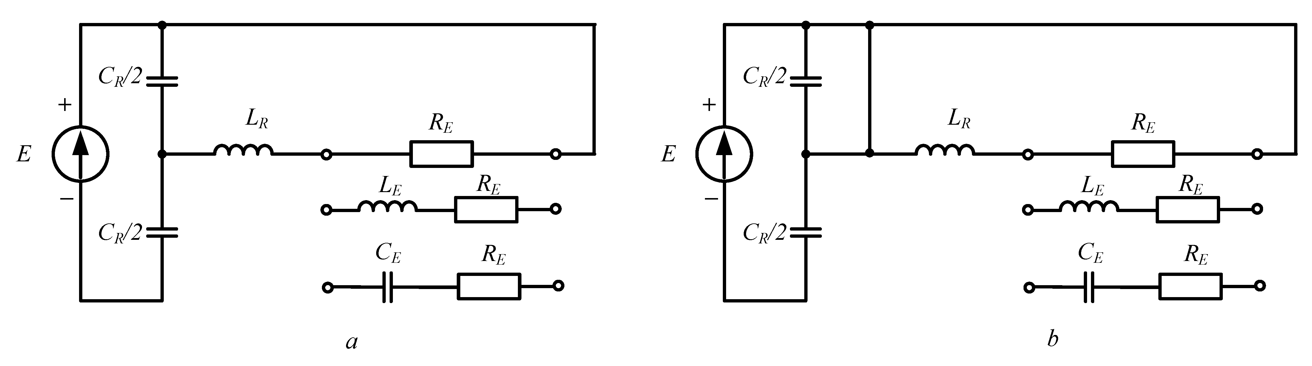
2. Basic Relations in the Analysis of Resonant DC/AC Converters with Energy Dosing

Different schematic variants of RI with ED are known [31,32]. In practice, any classic circuit of RI after adding restrictive diodes to limit the voltage on the resonant capacitor (capacitors) can be modified in RI with ED, since energy from the power source is consumed only through this capacitor, and with constant capacity, supply voltage and operating frequency, the power that is transmitted to the load does not change. Of the various topologies, the most convenient for physical implementation are the full-bridge circuit, the half-bridge circuit and the circuit with a split resonant capacitor, shown in Figure 1. On the other hand, it is known that the analysis of each of the known topologies is adapted to the specific power scheme by using numerical coefficients; thus, the analysis oriented to a particular scheme is applicable to all others. Due to the absence of filter capacitors required for half-bridge circuit prototyping, the split resonant capacitor circuit is more commonly used for the physical implementation of resonant converters. The specified power circuit is composed of two transistors with built-in reverse diodes VT1 and VT2, resonant inductance LR and a resonant capacitor composed of two identical parts—CR/2, limiting (dosing) diodes VD1 and VD2 and a parallel load circuit composed of an inductor with equivalent parameters L (inductive component of the load) and R (active component of the load) and a compensating capacitor C. The circuit is powered by a constant voltage source of magnitude E. The analysis assumes the ideality of all circuit elements.
Figure 2 shows the time diagrams of the inverter current and the voltage on the resonant capacitors, which visualize and represent the electromagnetic processes in the inverter.
From the view of the diagrams in Figure 2, it is concluded that within each half-period formed by the conduction of the corresponding transistor, three stages are observed: energy consumption from the power source (0 ÷ ϑd), one without consumption, which is characterized by a short circuit of the AC circuit d ÷ π-φ0), and a pause in which none of the semiconductor probes conducts but resonant processes of energy exchange between the load inductance L and the load capacitor C take place in the parallel load circuit.
When conducting the analysis of RI with ED, the following features are taken into account:
(1)
It is possible for the parallel load circuit to work on resonance, inductive or capacitive tuning (represented by the first harmonic as R, R-L, R-C) and together with the resonant elements of the circuit form an equivalent oscillating circuit with a frequency of angular natural oscillations ω0 (ω0 = 2.π.f0, f0—resonant frequency) greater than, less than or equal to the angular control frequency ω (ω = 2.π.f, f—working frequency);
(2)
The energy and power consumed by the power source and transmitted to the load by means of capacitors CR/2 are constant and independent of the load parameters;
(3)
The voltage uCR on the resonant capacitors is constant in the interval, and due to the operation of the limiting diodes, it is fixed at the level E/2 for the half-bridge scheme and E for the full-bridge scheme;
(4)
The voltage on the load uT in all appropriate/energy modes is sinusoidal;
(5)
The shape of the current pulse through the resonant inductance differs from the sinusoidal one, with the maximum shifted to the left of its middle. As a result, its first harmonic is also shifted to the left relative to the beginning of the half-period by an angle φ1. This circumstance should be taken into account in the analysis and design of the circuit, and the alternating voltages can be replaced by equivalent sinusoids, but in no case should this be done for the alternating current (due to its nonsinusoidal shape).
Usually, in the analysis of resonant converters, the following quantities are introduced:
  • δ—angle between the first harmonic of the generated voltage and the first harmonic of the current in the AC circuit. It is more convenient here to work with the tangent of this angle— t g δ = X E / R E = ( 1 / ω C E ) / R E , where CE and RE are the equivalent capacity and active resistance of the parallel load circuit, which are brought into the series resonance circuit of DC/AC converter;
  • Q—quality factor of a series resonant circuit
    Q = ω L R R E
  • ξ0, ξ—disturbances, respectively, of the parallel load circuit and of the series resonant circuit
    ξ 0 = ω 0 p ω , ξ = ω 0 ω ,
    where ω0p is the angular resonant frequency of the parallel load circuit, ω0 is the angular resonant frequency of the series AC circuit and ω is the angular control frequency;
  • cosφT—load power factor L-R
    cos φ T = R R 2 + ( ω L ) 2
A key place in the analysis of converters is the synthesis of the equivalent circuit of the AC circuit. On the one hand, it must be such that it most correctly reflects the properties and processes in DC/AC converters, while preserving the necessary accuracy of the obtained results. It is known that the actual electromagnetic processes in resonant inverters (RI) are determined by the number of reactive elements in the circuit. They determine the order of the differential equations describing them, and in connection with this, different resonant circuits are formed with the corresponding frequencies of the natural oscillations (when using complicated output circuits for matching the parameters of the inverter and the load). In this regard, by using the serial substitution scheme, the processes in RI are more realistically and accurately described. In a number of studies [26,28], it has been proven that this equivalent scheme has parameters close to those of the real one, and in a wide range of changing parameters, it can be used as a simplified, but sufficiently reliable, tool for describing the processes in RI. For this reason, precisely on the basis of the serial substitution scheme, the analysis was developed and the methodology for the design of RI with ED was compiled.

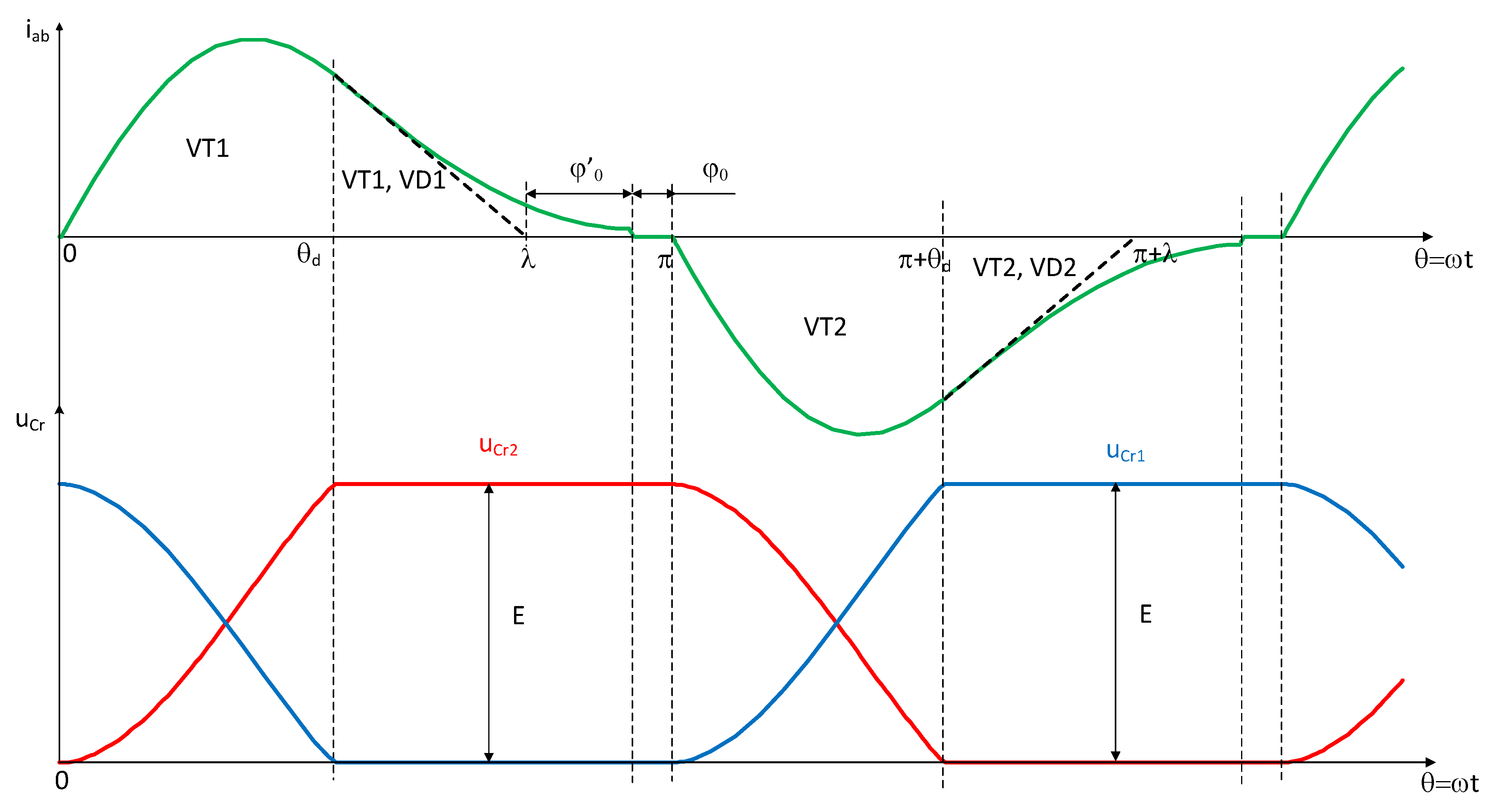
2.1. Features and Modes of Operation of the Inverter in the Interval of Energy Consumption from the Power Source

From the mode of action and from the theoretical studies of RI with ED, it is clear that in the interval 0 ÷ ϑd it is mandatory that the electromagnetic processes have an oscillatory character. For loads with a power factor cosφT = 0.05 ÷ 0.5, typical of electrotechnological devices, the frequency of oscillations of the alternating current circuit must be higher than the control frequency, i.e., ω0 > 1, to form a tendency for the current to drop to zero at the beginning of the pause φ0 between the two series of control pulses to the transistors VT1 and VT2. The continuation of the back front of the current pulse—see Figure 2 (line 2)—and its intersection with the abscissa axis determine the main intervals characterizing the three possible operating modes. In accordance with Figure 2, the following ratio between them is established [31,32]:
φ 0 = ( 0.65 ÷ 1.7 ) φ 0
In the most favorable operating mode (Figure 2), for pause values φ0 = 0.1π, the following angular frequency ratio can be assumed [31,32]:
ω 0 ω = π π φ 0 ( 0.65 ÷ 1.7 ) φ 0 > 1   and   ω 0 ω = 1.2 ÷ 1.4
The appropriate operating modes of the RI are unambiguously determined by the expression tgδ = (1.1 ÷ 1.5)ω0. If this dependence is not observed, it is difficult to assess the behavior of the RI—its operation can be assumed both in the mode with natural shutdown and in the mode with forced shutdown of the transistors, but with a frequency of self-oscillations ω0 determined by a random combination of its circuit elements.
It should be noted that with a load in the form of an oscillating circuit with a very high Q-factor (cosφT = 0.05 and less), a faster drop in current is observed in the interval ϑd ÷ π-φ0, where the natural shape of the current pulse and its approximating sinusoid converge sensitively and define a smaller ratio ω0, reaching 1.1 ÷ 1.2.
The modes in which the load circuit in the considered interval (0 ÷ ϑd) is set to resonance or close to resonance unambiguously determine, respectively, a relatively large and small value of the equivalent capacitor—CE and inductance—LE and their weak influence on the processes in the series substitute circuit shown in Figure 3 for one half-cycle of the operation of the power circuit. The resonant inductance LR, the capacitors CR1 and CR2 (CR1 = CR2 = CR) and the equivalent active resistance of the load RE have a dominant role regarding the nature of the electromagnetic processes. Therefore, their values determine the operating mode.
Taking into account the formulated requirements and the principle of operation of the power scheme, after solving the equation for the voltage on the resonant capacitors:
u C R ( ϑ d ) = 1 ω C R 0 ϑ d i ( ϑ ) = E ,   ( u C R ( 0 ) = E u C R ( ϑ d ) = E ) ,
the end of the interval of energy consumption by the power source is determined—the moment corresponding to angle ϑd.
Table 1 presents the equation for the AC current i(ϑ), its solution, which gives the expression for the inverter current in the considered interval, and the expression for determining the angle ϑd in the cases of a parallel load circuit set in resonance and with inductive or capacitive detuning.

2.2. Features and Modes of Operation of the Inverter in the Interval of the Short Circuit of the AC Circuit

The nature of the electromagnetic processes in the second interval ϑd ÷ π-φ0 is defined by the series circuit consisting of the short circuit through the plus or minus bus of the direct current power source, inductance LR and parallel resonant circuit (Figure 3b). Essentially, in most practical cases electromagnetic processes are aperiodic in nature, although an oscillatory mode is also possible. This is observed in the case of significant capacitive derangement of the load circuit. The current equations for the second interval at different equivalent parameters of the parallel load circuit are presented in Table 2.
Of very important practical value is the determination of the current value at the end of the considered interval (the moment corresponding to π-φ0), which sets the level of switching losses in transistors. It is calculated from the expression for the current I”(ϑ) at ϑ = π-φ0. In this regard, the expressions for the voltages on the resonant inductance LR and the parallel oscillating circuit uTm provide additional information about the electromagnetic processes in RI:
u L R = L d i d t ; u T m = R E [ i ( ϑ d ) e ϑ Q ] u C m = u C = u R E = i ( ϑ ) R E
It is obvious that if at the moment π-φ0 the AC current has zero value and the load circuit is set to resonance or close to resonance, then both the voltages uLR and uOUTm will also have a zero value. At this moment, the voltage on the transistor will also have a zero value, since in the considered interval the AC circuit consists of a short-circuited load circuit, a resonant inductance and a turn-on transistor. This circumstance deserves attention and should be evaluated as extremely favorable for the switching of transistors; that is, they will turn on at zero current and turn off at zero current and zero voltage. This condition is a basic requirement in the development of the operation algorithm of the control system. In this aspect, the control system must monitor and maintain a phase difference between the load circuit current and voltage equal to the pause between the control pulses φ0.

2.3. Determination of the Main Electrical and Phase Quantities in RI with ED

Analysis of RI with ED can be significantly facilitated by accepting the voltage of the resonance capacitor uCR as a sine wave truncated above and below at the level E/2 (for the full-bridge version this voltage is equal to E), according to Figure 4. The amplitude UCRm in this case is determined by the expression:
U C R m = E / 2 cos τ / 2 = I m 1 C R ω o
With an active load or set to operate in a resonant load circuit, the voltages UOUTm = UCm, UACm are obtained from the form:
U O U T m = U C R m / sin δ   and   U A C m = U O U T m cos δ ,
where UACm is the voltage across the entire AC circuit of the RI converter.
The values of the load parameters and their change are expressed by the generalized parameters and Q and, indirectly, by the parameters of the current pulse—ϑm, ϑd, Im. In the most favorable mode of operation—a load circuit set in resonance—the alternating current has an oscillatory character in the interval 0 ÷ ϑd and aperiodic in ϑd ÷ π-φ0. The frequency of natural oscillations ω0 and the value of angle δ (tgδ) are determined by the expression (5) and the considerations formulated regarding the operating modes of RI with ED.
When determining the remaining parameters of the current pulse, the specifics of the mode of operation of the circuit must be taken into account, which in this case is expressed by the presence of two intervals of operation and, respectively, two equivalent circuits within one half-period of the control frequency. Accordingly, for the maximum value of the AC current the expression is valid:
I V T m = E ω 0 ω ω L R e ϑ m 2 Q sin ω 0 ω ϑ m ,
where ϑm is the argument of the extremum di(ϑ)/dϑ = 0, i.e.,
ϑ m = a r c t g 2 Q ( ω 0 / ω ) ( ω 0 / ω )
Based on (10) and (11), the expression for determining the moment corresponding to ϑd is written in the following form:
ϑ d = π ω 0 / ω ϑ m = π τ = π 2 arccos E c o t g δ 2 U O U T m
The currents flowing through the semiconductor devices are determined by the corresponding equations for the AC current in the two intervals 0 ÷ ϑd and ϑd ÷ π-ϕ0 (see Table 1 and Table 2). In the case that the RI works with zero current on and off, the reverse diodes are not turned on (i.e., IVDT1 = IVDT2 = 0).
Thus, the average current of transistors and dosing diodes VD1, VD1 (see Figure 2) when operating in this mode is calculated by the expression:
I V T o = 1 2 π [ 0 ϑ d i ( ϑ ) d ϑ + 0 π ϑ d φ 0 i " ( ϑ ) d ϑ ] = E f C R ( 1 + e π φ 0 2 Q )
I V D o = 1 2 π ϑ d π φ 0 i " ( ϑ ) d ϑ = I m V D 2 π Q ( 1 e π ϑ d φ 0 Q )
The consumed current from the power source is determined by the ratio expressing the constant power in RI with ED:
P = E 2 C R f = E I 0 , I 0 = C R f E
or from by using the expression to determine its average value:
I 0 = 1 π 0 π ϑ d i ( ϑ ) d ϑ = E f C R
From the presented expressions, it is found that the current I0 and the power are proportional to the frequency. This circumstance is successfully used for power regulation, as well as for protecting the RI from overload. Based on the expressions (13) and (14), the average current of the metering diodes is determined by using simpler ratios:
I V D o = I V T o I 0 = E C R f ( 1 e π φ 0 2 Q ) E C R f = E C R f e π φ 0 2 Q
A criterion for the validity of the analysis is that the same expression for the current IVDo can be obtained from the ratio:
I V D o = 1 2 π 0 π ϑ d i " ( ϑ ) d ϑ = E f C R e π φ 0 2 Q
The value of this current is not only the basis for choosing the diodes VD1 and VD2. It also brings additional information, both about the type of electromagnetic processes and about the operating mode of RI with ED.

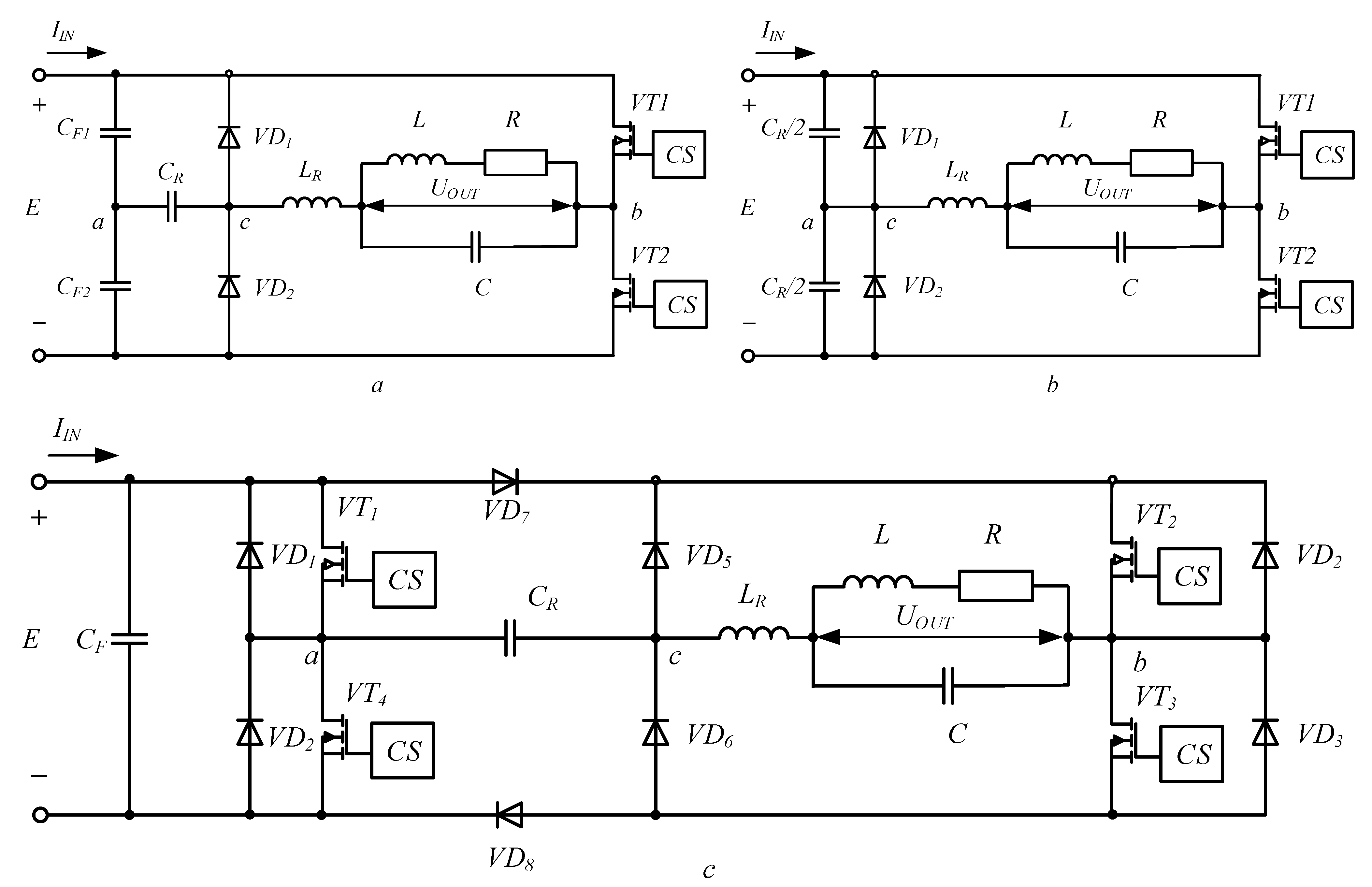
3. Methodology for Engineering Design of RI with ED

It should be noted that the design process of a power electronic device is a complex and multifaceted task. The complexity arises from the fact that the load as part of the scheme is highly variable during a real technological process. The diversity of the task consists in the fact that it is necessary to change according to a certain law the output values of the RI in order to implement the different technological modes and agree with the parameters of the load. The satisfaction of the specified requirements is defined mainly by the technical specification, and this turns the design into a process with multifactor optimization, the limiting conditions of which are functionally linked to the characteristics of the load and the correct description of the transient and stationary operating modes of the device.
RI with ED has strictly individual qualities, concretizing the following specific design requirements:
(1)
The engineering design of the RI power circuit and the load is a joint process in which the RI design plays a dominant role. The determination of the voltage uCR, which is also the load voltage, is a key point in determining its equivalent active resistance R and inductance L;
(2)
It is necessary that the phase difference between the current and the voltage of the load parallel resonant circuit is equal to the pause between the control pulses of the transistors and is maintained in this state by the control system in the process of operation. In such an operating mode, the transistors work with soft commutations—they turn on at zero current and zero voltage. To satisfy the specified condition, the frequency of natural oscillations of the equivalent circuit of the AC circuit of the RI must be greater than the control frequency, i.e., ω0 > 1. The research carried out in [31,32] showed that at values of the pause between the control pulses, most often φ0 = 0.1π, ω0p/ω = 1.2–1.4 can be assumed;
(3)
The energy and power consumed by the power source and transferred to the load through the capacitor CR are unchanged;
(4)
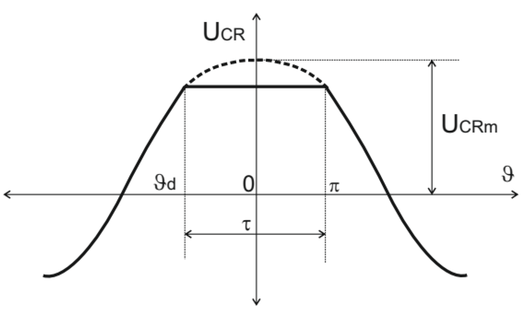
The voltage of the resonant (dosing) capacitors in the interval ϑd ÷ π can be considered a truncated top and bottom cosine at the level E/2 or E, respectively, for the half-bridge and full-bridge circuit variants;
(5)
Regardless of the diversity of the task related to RI operation modes and load change limits, the following initial data for the design are unambiguously defined: (1) power of the converter; (2) operating frequency; (3) load parameters and range of their change; (4) DC power source voltage.
Taking into account the properties, analytical relationships and considerations for the selection of quantities, with a view to providing an optimal (from the point of view of harmonic composition) current pulse through the transistors and maintaining a constant power in the load, the following sequence of calculation procedures is recommended at the design of the bridge and half-bridge RI with ED with and without reverse diodes of the transistors:
(1)
The pause φ0 is initially set. Its size is determined depending on the required operating frequency and catalog switching times of the transistors. For example, a suitable value for this parameter is the following: φ0 = 0.1π.
(2)
The ratio value ω0p/ω = 1.2–1.4 is selected. Most often, a value of ω0p/ω = 1.3 is chosen, and this ratio is adjusted during the design process if necessary.
(3)
The phase angle δ is determined, according to the fundamental ratio [31] for RI—tgδ > (1.2–1.4) ω0.
(4)
Based on the set power and operating frequency, the value of the resonant capacitor CR is calculated:
C R = P E 2 f
(5)
The detuning at which the voltage and current through the parallel circuit will have a phase—ψ is determined by the expression:
ξ 0 2 = t g φ + c o t g φ t g φ + t g ψ
It is proven that at the resonance of the load circuit along the first harmonic of the AC current, having a phase φ1, the angle ψ is defined by the expression ψ = φ 1 φ 0 . From the repeated calculations and studies carried out on the shape and parameters of the current pulse, it can be recommended to start the design at the smallest value of angle ψ for which the parallel circuit is in resonance, i.e., ψ ≈ 0.
(6)
For the selected value of tgδ and the detuning obtained according to (19), the real and relative values of the equivalent resistance of the load circuit are determined:
R E = 1 ω C R t g δ ; R E = ξ 0 2 c o t g φ ( ξ 0 2 1 ) 2 + c o t g 2 φ
(7)
The value of the parallel capacitor C is found from the expression:
C = 1 / ( ξ 0 2 ω 2 L T )
(8)
From the load circuit resonance condition, the substitution circuit elements R, L and the load voltage are determined:
L = 1 ξ 0 2 ω C , R = ω L c o t g φ , U L m = 2 P R cos φ .
The method of calculating the voltage on the load uT predetermines certain specifics in the design of this type of RI. The physical essence of obtaining the voltage uT is a consequence of the peculiarities of the ED method, consisting in fixing the power level and the voltage of the capacitor CR, at zero values of the alternating current at the moments ϑ = 0 and ϑ = π-φ0. For this reason, the exact value of the voltage uT is determined not by the calculation procedure of the load but by the selected inverter parameters ω0, δ and the value of the constant supply voltage E. This means that the number of windings of the induction heater or the translation ratio of the matching transformer are a consequence of the circuit elements and magnitudes from the RI, and not vice versa.
It should be clarified that the voltage uT thus obtained is not the only one possible for the specific values of the resonant elements LR and CR, as well as for the selected value of the capacitor C. When changing the load equivalent parameters, as a result unloading the induction heater or replacing it with another, requiring a voltage different from that calculated by (20), the power with which the RI works is preserved. The necessary voltage on the circuit is obtained thanks to the metering of the energy and the resulting property of the RI to operate at a constant power. The described phenomenon means that the RI adapts itself to the specific load. However, with the change in the load, the corresponding change in the operation mode of the RI is noticed, i.e., transistors turn on and/or off at nonzero current. By changing the control frequency through the control system—for example, with a PLL type controller—the necessary and sufficient condition for the switching of the transistors at zero current (ZCS) consists in maintaining a phase φ0 between the voltage and the current of the parallel load circuit. All this practically means that when choosing the parameters ω0/ω and tgδ according to the design procedure and supply voltage E = 500 V, the output voltages of the half-bridge RI with ED are in the range 200 ÷ 300 V, and for the full-bridge—300 ÷ 500 V.
(9)
A particularly important place in the design methodology is the determination of the moment ϑd, which provides information about the end of the interval of energy consumption from the power source and the beginning of the short circuit through the plus or minus bus of the input power source. For the value of ϑd, it is obtained:
ϑ d = π ω 0 / ω a r c t g 2 Q ω 0 / ω ω 0 / ω
(10)
From the expression U O U T m = U A C m cos δ = U C R m cos δ sin δ = E cos π ϑ d 2 c o t g δ
, is calculated accordingly τ = π ϑ d , τ = 2 arccos E c o t g δ 2 U O U T m .
(11)
By numerically solving equation: ϑ d ω 0 ω + a r c t g 2 Q ω 0 ω = π , where
Q = 1 2 ( 1 ω 0 / ω ) 2 [ t g δ + t g 2 δ ( ω 0 / ω ) 2 ]
a check is carried out, and, if necessary, the attitude is specified ω0. The quality factor Q of the equivalent AC replacement circuit of the inverter is also found.
(12)
The resonant inductance LR is calculated with the value of the generalized parameter Q obtained according to (11):
L R = Q R E ω
(13)
The maximum values of the voltages UOUTm and UCRm are, respectively, equal:
U A C m = U O U T m cos δ , U C R m = U A C m sin δ = E cos ( π ϑ d 2 )
(14)
The average and maximum values of the current through the transistors and diodes are determined by the following expressions:
(a)
Full-bridge version (Figure 1c)
I V S 1 , 4 o = I V D 7 , 8 o = E f C R 2 = I 0 2
I V S 2 , 3 o = 1 2 π 0 π i ( ϑ ) d ϑ = E f C R ( 1 + e π φ 0 2 Q )
I V D 5 , 6 o = 1 2 π 0 π ϑ d i " ( ϑ ) d ϑ = E f C R e π ϑ d 2 Q
I V D 5 , 6 m = i ( ϑ d ) = E ω 0 ω ω L R e ϑ d 2 Q sin ω 0 ω ϑ d
I V S 1 ÷ 4 m = I V D 7 , 8 m = i ( ϑ m ) = E ω 0 ω ω L K e ϑ m 2 Q sin ω 0 ω ϑ m
(b)
Half-bridge version (Figure 1a)
I V S 1 , 2 o = 1 2 π 0 π i ( ϑ ) d ϑ = E f C R ( 1 + e π φ 0 2 Q )
I V S 1 , 2 m = i ( ϑ m ) = E ω c k ω ω L R e ϑ m 2 Q sin ω 0 ω ϑ m
I V D 3 , 4 m = i ( ϑ d ) = E ω 0 ω ω L R e ϑ d 2 Q sin ω 0 ω ϑ d
I V D 3 , 4 o = 1 2 π 0 π ϑ d i " ( ϑ ) d ϑ = E f C R e π ϑ d 2 Q
(15)
The moment ϑm at which the current through the transistor has a maximum value is determined by the expression:
ϑ m = a r c t g 2 Q ω 0 ω ω 0 / ω
(16)
The average current consumed by the power source is equal to the difference between the current of the transistors and the dosing diodes:
I 0 = I V T o I V D o = E C R f ( 1 + e π ϑ d 2 Q ) E C R f e π ϑ d 2 Q = E C R f
Based on the ratio expressing the constant power in RI with ED, the average current consumed by the power source is also found:
P = E 2 C R f = E I 0 , I 0 = E f C R
As can be seen, current and power are proportional to frequency. This circumstance is used for power regulation as well as to protect the RI from overload.
The mismatch of the calculated consumer current according to expressions (36) and (37) is a sign of an error in the calculations or of an inaccurately set ratio ω 0 / ω , and the calculation procedure should be repeated until the problem is eliminated.

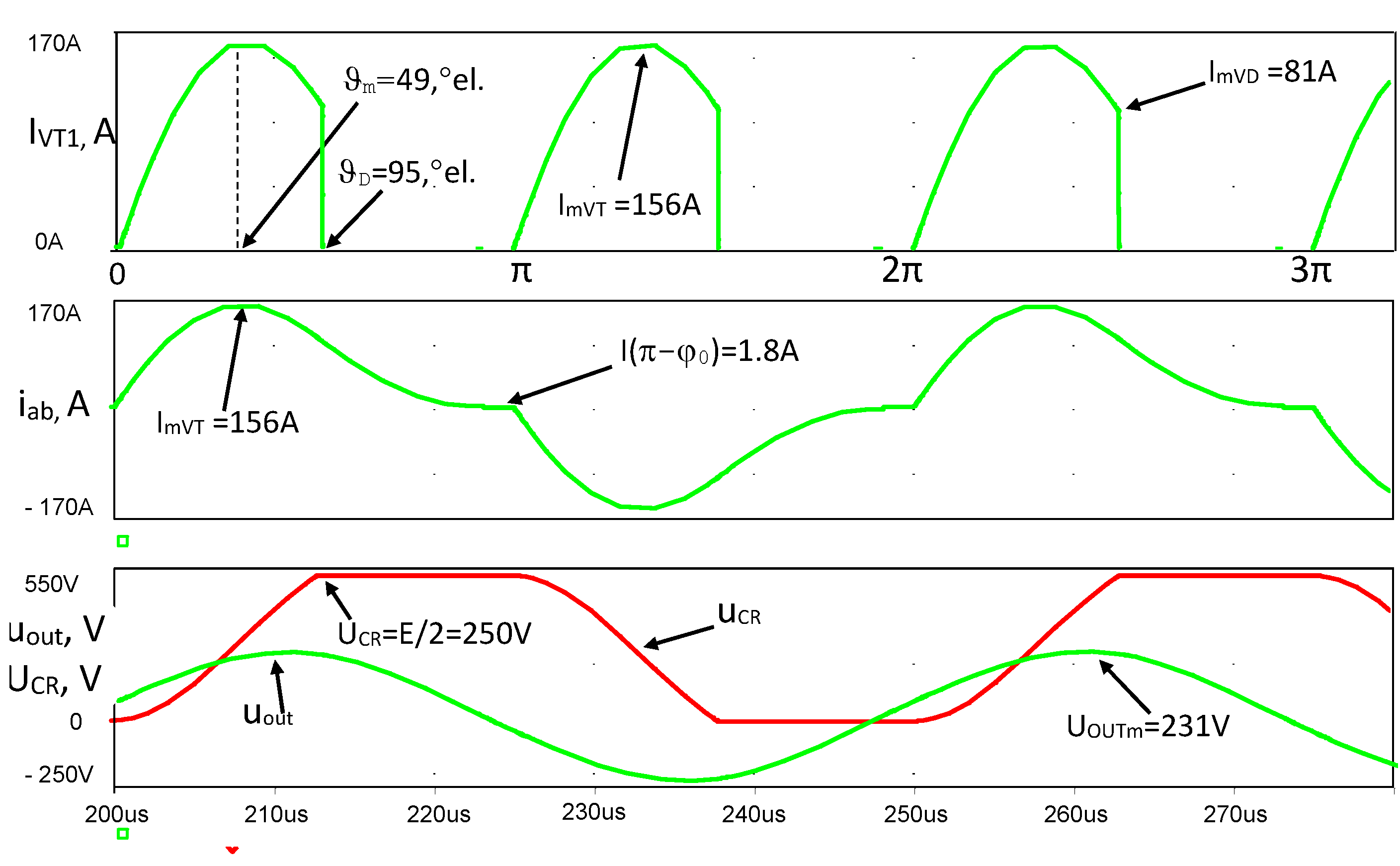
4. Verification of the Design Procedure

According to the given methodology, a half-bridge RI with energy dosing and split resonant capacitor (Figure 1b) was designed with the following input data: output active power P = 15 kW; operating frequency f = 20 kHz; load power factor cos φ = 0.17; angle of the current break in the AC circuit φ0 = 0.1π; DC supply voltage E = 500 V.
The calculated and computer simulation values of the elements and quantities are given in Table 3, and the time diagrams of currents and voltages obtained as a result of computer simulations are presented in Figure 5. The load has an active-inductive nature and is represented by its equivalent active R and inductive L resistances. The resulting phase and electrical parameters from the design and analysis are interpreted in Figure 5.
To prove the reliability of the analysis and the methodology for designing RI with ED, practical experiments were carried out with the purpose-built transistor (with IGBT) frequency converter with the following technical parameters: output power P = 5–15 kW; operating frequency f = 10–30 kHz; DC supply voltage E = 500 V.
Tests and research were done with three typical induction heating loads: an induction furnace for melting ferrous and nonferrous metals; a high-resistance inductor for volumetric heating of steel blanks; and inductors for surface heat treatment.
In the case of an induction furnace, the power is kept equal to the set (nominal) during the entire technological process—from the cold state of the metal to its melting; in a full and partially filled furnace with metal; and in ceramic and graphite crucibles. The converter operates safely with an empty furnace (with self-reduced power due to the load self-adaptation property of RI with ED) as well as with partial or full short-circuiting of the inductor windings.
With a load in the form of a high-resistance inductor, the operation of the converter is analogous—P = const for different numbers of blanks in the inductor, while at idle the power naturally decreases, and the voltage increases by no more than 30% compared to the nominal one.
In the case of working with surface heat treatment inductors that are low resistance, the output voltage is stepped down by a transformer to a low base value. Then, inductors with different diameters (from D = 10 mm to D = 35 mm), with the number of windings W = 1 and W = 2, were connected to the converter. The power is kept P = const without adjusting the transformer.
The results of the research of the three typical induction heating loads are summarized in Figure 6. The figure presents a characteristic taken experimentally of the converter described, as well as any other converters constructed using the principle of energy dosing. The characteristic manifests the dependence of the output voltage and the power on the load resistance. It can be seen that when the load resistance Z increases, the voltage rises, and what is more, it rises sufficiently to keep the power constant. The presented parameters are in relative units—ratio of the current value to the nominal value (with subscript N).
Two other types of research were also conducted. As a variable load, a high-resistance inductor is used, switched on without a matching transformer, a calorimeter with a diameter DC = 100 mm and a height equal to that of the inductor. The values of all the main parameters of the mode at P = 5 kW and f = 20 kHz are presented in Table 4. They are almost the same from design, computer and real experiments.
From the comparison between the results obtained by different means (analytical, simulation and experimental), it is established that the proposed design procedure gives good accuracy (difference in the values of the individual quantities below 5%).

5. Conclusions

This article presents a design procedure for a resonant DC/AC converter with energy dosing with induction heating applications. Based on an analysis of the operation of the power circuit, the main dependencies describing the electromagnetic processes have been derived. By means of these expressions, the basic ratios with which all the schematic elements are selected are defined. The presented methodology has been verified through computer simulations and prototype experiments. A natural continuation of the current research is, based on mathematical modeling and using mathematical software, to determine the optimal values of the circuit elements for various target functions: minimum losses, maximum efficiency, minimum dimensions and others.
The main advantage of energy-metering schemes is that the power does not depend on the load and they are self-adaptive to change. Therefore, during a real technological process of induction heating, when the equivalent load is constantly changing (due to the change in temperature), the power transmitted to the load is constant. A disadvantage of the presented schemes with energy dosing is the complicated topology and the uneven load of the transistors (in the case of the full-bridge scheme), and also that the average value of the current consumed by the power source is limited, while the current through the transistors, especially when operating in inappropriate modes, can reach very large values (5–10 times the average value).

Author Contributions

N.M. and N.H. were involved in the full process of producing this paper, including conceptualization, methodology, modeling, validation, visualization and preparing the manuscript. All authors have read and agreed to the published version of the manuscript.

Funding

This research was funded by European Regional Development Fund, grant number BG05M2OP001-1.001-0008 and KII-06-H37/25/18.12.2019 and the APC was funded by European Regional Development Fund.

Institutional Review Board Statement

Not applicable.

Informed Consent Statement

Not applicable.

Data Availability Statement

Not applicable.

Acknowledgments

The research was supported by the European Regional Development Fund within the Operational Programme “Science and Education for Smart Growth 2014–2020” under the Project CoE “National center of mechatronics and clean technologies “BG05M2OP001-1.001-0008 and “Optimal design and management of electrical energy storage systems” (KII-06-H37/25/18.12.2019), Bulgarian National Scientific Fund.

Conflicts of Interest

The authors declare no conflict of interest.

References

  1. Desisa, D. Numerical Modeling of Induction Heating Process Control. In Proceedings of the 22nd International Scientific Conference on Electric Power Engineering (EPE), Kouty nad Desnou, Czech Republic, 8–10 June 2022; pp. 1–6. [Google Scholar] [CrossRef]
  2. Kovac, D.; Melnykov, V. Simulation and Laboratory Model of Induction Heating in COMSOL Multiphysics. In Proceedings of the IEEE International Conference on Modern Electrical and Energy Systems (MEES), Kremenchuk, Ukraine, 21–24 September 2021; pp. 1–6. [Google Scholar] [CrossRef]
  3. Rasheed, F.A.; Abdulbaqi, I.M. Analysis of a Current-Fed Parallel Resonant Inverter for Induction Heating Applications. In Proceedings of the 1st Babylon International Conference on Information Technology and Science (BICITS), Babil, Iraq, 28–29 April 2021; pp. 169–173. [Google Scholar] [CrossRef]
  4. Vishnuram, P.; Ramachandiran, G.; Babu, T.S.; Nastasi, B. Induction Heating in Domestic Cooking and Industrial Melting Applications: A Systematic Review on Modelling, Converter Topologies and Control Schemes. Energies 2021, 14, 6634. [Google Scholar] [CrossRef]
  5. Lucia, O.; Maussion, P.; Dede, E.J.; Burdio, J.M. Induction Heating Technology and Its Applications: Past Developments, Current Technology, and Future Challenges. IEEE Trans. Ind. Electron. 2013, 61, 2509–2520. [Google Scholar] [CrossRef]
  6. Meinert, J.D.; Kjærsgaard, B.F.; Aunsborg, T.S.; Jorgensen, A.B.; Munk-Nielsen, S.; Duun, S.B. Class-E Push-Pull Resonance Converter with Load Variation Robustness for Industrial Induction Heating. In Proceedings of the 2022 24th European Conference on Power Electronics and Applications (EPE’22 ECCE Europe), Hannover, Germany, 5–9 September 2022; pp. 1–8. [Google Scholar]
  7. Sarnago, H.; Lucia, O.; Burdio, J.M. High-Performance Class-E Quasi-Resonant Inverter for Domestic Induction Heating Applications. In Proceedings of the 2022 IEEE Applied Power Electronics Conference and Exposition (APEC), Orlando, FL, USA, 19–23 March 2022; pp. 1202–1207. [Google Scholar] [CrossRef]
  8. Han, W.; Chau, K.T.; Liu, W.; Tian, X.; Wang, H. A Dual-Resonant Topology-Reconfigurable Inverter for All-Metal Induction Heating. IEEE J. Emerg. Sel. Top. Power Electron. 2021, 10, 3818–3829. [Google Scholar] [CrossRef]
  9. Herasymenko, P.; Yurchenko, O. An Extended Pulse-Density-Modulated Series-Resonant Inverter for Induction Heating Applications. In Proceedings of the 2020 IEEE 61th International Scientific Conference on Power and Electrical Engineering of Riga Technical University (RTUCON), Riga, Latvia, 5–7 November 2020; pp. 1–8. [Google Scholar] [CrossRef]
  10. Ivanov, A.; Bukanin, V.; Zenkov, A.; Vologdin, V.; Vologdin, V. Cyber Physical Systems Integration for Induction Heating Technologies. In Proceedings of the 2020 9th Mediterranean Conference on Embedded Computing (MECO), Budva, Montenegro, 8–11 June 2020; pp. 1–4. [Google Scholar] [CrossRef]
  11. Panchal, S.; Kulkarni, R.; Raja, M.K.; Nataraj, J. Design, Simulation and Hardware Implementation of Soft Switching based Induction Heating System. In Proceedings of the 2021 6th International Conference for Convergence in Technology (I2CT), Maharashtra, India, 2–4 April 2021; pp. 1–7. [Google Scholar] [CrossRef]
  12. Salehi, S.; Abbaszadeh, K.; Sani, S.G.; Mohamadi, H.H. A new Domestic Induction Heating Resonant Converter with High Power Conversion Efficiency. In Proceedings of the 2021 12th Power Electronics, Drive Systems, and Technologies Conference (PEDSTC), Tabriz, Iran, 2–4 February 2021; pp. 1–6. [Google Scholar] [CrossRef]
  13. Hawryluk, M.; Rychlik, M.; Pietrzak, M.; Górski, P.; Marzec, J. Development of Induction Heating System Ensuring Increased Heating Efficiency of the Charge Material in a Forging. Materials 2022, 15, 1516. [Google Scholar] [CrossRef] [PubMed]
  14. Perevalov, Y.Y.; Demidovich, V.B. Intelligent Design and Control System of Automated Installations for Induction Heating of Products. In Proceedings of the 2022 22nd International Symposium on Electrical Apparatus and Technologies (SIELA), Bourgas, Bulgaria, 1–4 June 2022; pp. 1–5. [Google Scholar] [CrossRef]
  15. Phankong, N.; Chudjuarjeen, S.; Chakkuchan, P.; Nawong, M. Preheat Welding with Induction Heating Based Control of Phase-Locked Loop Resonant Inverter. In Proceedings of the 2022 International Electrical Engineering Congress (iEECON), Khon Kaen, Thailand, 9–11 March 2022; pp. 1–4. [Google Scholar] [CrossRef]
  16. Park, N.-J.; Lee, D.-Y.; Hyun, D.-S. A Power-Control Scheme with Constant Switching Frequency in Class-D Inverter for Induction-Heating Jar Application. IEEE Ind. Electron. Mag. 2007, 54, 1252–1260. [Google Scholar] [CrossRef]
  17. Sankhe, D.N.; Sawant, R.R.; Rao, Y.S. FPGA-Based Hybrid Control Strategy for Resonant Inverter in Induction Heating Applications. IEEE J. Emerg. Sel. Top. Ind. Electron. 2021, 3, 156–165. [Google Scholar] [CrossRef]
  18. Ngo-Phi, T.; Nguyen-Quang, N. Variable Pulse Density Modulation for Induction Heating. In Proceedings of the 2021 International Symposium on Electrical and Electronics Engineering (ISEE), Ho Chi Minh, Vietnam, 15–16 April 2021; pp. 226–231. [Google Scholar] [CrossRef]
  19. Lee, Y.-L.; Lin, C.-H.; Liu, H.-D. A Novel MPPT Heating Control Strategy Applied to the Induction Heating System. Processes 2022, 10, 1151. [Google Scholar] [CrossRef]
  20. Oh, Y.; Yeon, J.; Kang, J.; Galkin, I.; Oh, W.; Cho, K. Sensorless Control of Voltage Peaks in Class-E Single-Ended Resonant Inverter for Induction Heating Rice Cooker. Energies 2021, 14, 4545. [Google Scholar] [CrossRef]
  21. Artal-Sevil, J.S.; Rivases, F.; Beyza, J.; Evangelista, M.A. Design and Implementation of a High-Power Resonant Converter for an Induction Steel-Melting Furnace. In Proceedings of the 2021 IEEE International Autumn Meeting on Power, Electronics and Computing (ROPEC), Ixtapa, Mexico, 10–12 November 2021; pp. 1–6. [Google Scholar] [CrossRef]
  22. Villa, J.; Navarro, D.; Dominguez, A.; Artigas, J.I.; Barragan, L.A. Vessel Recognition in Induction Heating Appliances—A Deep-Learning Approach. IEEE Access 2021, 9, 16053–16061. [Google Scholar] [CrossRef]
  23. Lucia, S.; Navarro, D.; Karg, B.; Sarnago, H.; Lucia, O. Deep Learning-Based Model Predictive Control for Resonant Power Converters. IEEE Trans. Ind. Informat. 2020, 17, 409–420. [Google Scholar] [CrossRef]
  24. Kouro, S.; Perez, M.A.; Rodriguez, J.; Llor, A.M.; Young, H.A. Model Predictive Control: MPC’s Role in the Evolution of Power Electronics. IEEE Ind. Electron. Mag. 2015, 9, 8–21. [Google Scholar] [CrossRef]
  25. Bedford, B.D.; Hoft, R.G. Principles of Inverter Circuits; John Wiley & Sons: New York, NY, USA, 1964; ISBN 978-0471061342. [Google Scholar]
  26. Mohan, N.; Undeland, T.M.; Robbins, W.P. Power Electronics—Converters, Applications, and Design, 3rd ed.; John Wiley & Sons: Hoboken, NJ, USA, 2003. [Google Scholar]
  27. Kazimierczuk, M.K.; Czarkowski, D. Resonant Power Converters, 2nd ed.; IEEE Press and John Wiley & Sons: New York, NY, USA, 2011; pp. 1–595. ISBN 978-0-470-90538-8. [Google Scholar]
  28. Dokić, B.L.; Blanuša, B. Power Electronics Converters and Regulators, 3rd ed.; Springer International Publishing: Cham, Switzerland, 2015; ISBN 978-3-319-09401-4. [Google Scholar]
  29. Rashid, M.H. Power Electronics Handbook: Devices, Circuits, and Applications; Academic Press: Burlington, MA, USA, 2007. [Google Scholar]
  30. Erickson, R.W.; Maksimovic, D. Fundamentals of Power Electronics, 2nd ed.; Kluwer Academic Publishers Group: Norwell, MA, USA, 2001. [Google Scholar]
  31. Todorov, T.S.; Madzharov, N.D.; Alexiev, D.T.; Ivanov, P.T. Autonomous Inverters; Technical University of Gabrovo: Gabrovo, Bulgaria, 1996. [Google Scholar]
  32. Madzharov, N. High-Frequency Power Source with Constant Output Power. J. Eng. Sci. Technol. Rev. 2016, 9, 157–162. [Google Scholar] [CrossRef]
Figure 1. Schematic variants of RI with ED (a) half-bridge circuit; (b) with split resonant capacitor; (c) full-bridge circuit.
Energies 16 01462 g001
Figure 2. Timing diagrams in established operation mode of RI with ED and split resonance capacitor.
Energies 16 01462 g002
Figure 3. Equivalent scheme for one half-period of the operation of RI with DE (a) with power consumption from the power source (0 − ϑd); (b) without power consumption from the power source d − π).
Energies 16 01462 g003
Figure 4. Voltage across the resonant capacitor.
Energies 16 01462 g004
Figure 5. Timing diagrams of half-bridge RI with ED and split resonant capacitor—computer experiment.
Energies 16 01462 g005
Figure 6. Dependence of the output voltage and power on the variation of the load.
Energies 16 01462 g006
Table 1. Mathematical expressions describing the first interval of the scheme’s operation.
Interval 0 ÷ ϑd
Type of LoadDifferential Equation for the Inverter Current i1Solution of Differential Equation for i1Solution for ϑd
R 1 2 C R i 1 d t + L R d i 1 d t + i 1 R E = E i 1 ( ϑ ) = E ω 0 ω ω L R e ϑ 2 Q sin ω 0 ω ϑ
Q = R E / ω L R
ϑ d = π a r c t g 2 Q ω 0 ω ω 0 ω
L-R 1 2 C R i 1 d t + L A C d i 1 d t + i 1 R E = E
L A C = L R + L E
LE, RE—equivalent inductance and active resistance of the load circuit;
LAC—equivalent inductance of the AC circuit.
i 1 ( ϑ ) = E ω 0 ω ω L A C e ϑ 2 Q E sin ω 0 ω ϑ
Q E = R E / ω ( L R + L E )
ϑ d = π a r c t g 2 Q E ω 0 ω ω 0 ω
C-R 1 C A C i 1 d t + L R d i 1 d t + i 1 R E = E U C E ( 0 )
C A C = 2 C R C E 2 C R + C E ;
CAC—equivalent capacity of the AC circuit;
CE, RE—equivalent capacitance and active resistance of the load circuit.
i 1 ( ϑ ) = E u C E ( 0 ) ω 0 ω ω L R e ϑ 2 Q sin ω 0 ω ϑ
u C E ( 0 ) = E ( e ϑ 2 Q + 1 ) ( e ϑ 2 Q + 1 ) + 4 C R ( C A C 2 C R )
Q = R E / ω L R
1 = 2 ( 1 2 C R C A C ) ( e ϑ 2 Q + 1 ) 4 C R C A C . [ e ϑ 2 Q ( 1 2 Q sin ω 0 ω ϑ cos ω 0 ω ϑ ) + 1 ]
Table 2. Mathematical expressions describing the second interval of the operation of the scheme.
Interval ϑd ÷ π-φ0
Type of LoadDifferential Equation for the Inverter Current i1Solution of Differential Equation for i1
R L R d i " d t + R E i " = 0 i " ( ϑ ) = i ( ϑ d ) e R E ω L R ϑ
L-R L R d i " d t + L E d i " d t + R E i " = 0 i " ( ϑ ) = i ( ϑ d ) e R E ω ( L R + L E ) ϑ
C-R L R d i " d t + R E i " + 1 C E i " d t + u C E ( 0 ) = 0
u C E ( 0 ) = u C E ( ϑ d ) i " ( 0 ) = i ( ϑ d )
roots of the characteristic equation:
p 1 , 2 = δ ± δ 2 ω 2 δ = R E 2 L R ω = 1 L R C E
(1) δ > ω —aperiodic mode
i ( ϑ ) = p 1 [ p 2 . C e . U c 2 ( ϑ d ) i ( ϑ d ) . [ e p 1 . ϑ ω . t p 2 [ i ( ϑ d ) p 1 . C e . U c e ( ϑ d ) . e p 2 . ϑ ω p 2 p 1
(2) δ = ω —critical-aperiodic mode
i " ( ϑ ) = [ i ( ϑ d ) + p . i ( ϑ d ) . ϑ ω p . C E . U C E . ( ϑ d ) ϑ ω ] . e P ϑ ω
(3) δ < ω —resonant mode
i " ( ϑ ) = C E . A . e δ ϑ ω 0 [ ϑ . ω ( ϑ + x ) δ . sin ( ϑ + x ) ]
x = a r c   c o t g i ( ϑ d ) + C E . U C E ( ϑ d ) ϑ . C E . U C E ( ϑ d )
A = ϑ . C E . U C E ( ϑ d ) + [ i ( ϑ d ) + δ . C E . U C E . ( ϑ d ) ω . C E
Table 3. Half-bridge RI with ED and split resonant capacitor: design and computer simulation results.
Schematic Element Values: Load Parameters: R = 0.05 Ω; L = 2.3 μH; LR = 11.1 μH; CR/2 = 1.5 μF
Dimensionϑm, ° ϑD, ° UOUTm, VI0, AImVT, AIOVT, AImVD, AIOVD, AP, kWI(π-t0), A
Calculated46932303015133.2813.23152.3
Simulated49952313015633.2883.8151.8
Table 4. Half-bridge RI with ED: design and computer simulations results.
Schematic Element Values: P = 5 kW; f = 20 kHz; E = 295 V; R = 0.05 Ω; L = 2.3 μH; LR = 11.1 μH; CR/2 = 1.5 μF
Dimensionφm,°φd,°UOUTm,VI0, AIVT1,2m, AIVT1,2o, AID3,4m, AID3,4, AI(π-φ0), A
Calculated45.596.31491785.618.447.91.40.9
Simulated44.895.1146.816.98618.548.11.50.8
Measured4596148178518.449.51.40.9
Disclaimer/Publisher’s Note: The statements, opinions and data contained in all publications are solely those of the individual author(s) and contributor(s) and not of MDPI and/or the editor(s). MDPI and/or the editor(s) disclaim responsibility for any injury to people or property resulting from any ideas, methods, instructions or products referred to in the content.

