Review

Noise Spectroscopy: A Tool to Understand the Physics of Solar Cells

by
Giovanni Landi
1,
Sergio Pagano
2,3,4,*,
Heinz Christoph Neitzert
5,
Costantino Mauro
3 and
Carlo Barone
2,3,4
1
ENEA, Portici Research Center, Piazzale Enrico Fermi 1, 80055 Portici, NA, Italy
2
Dipartimento di Fisica “E.R. Caianiello”, Università degli Studi di Salerno, 84084 Fisciano, SA, Italy
3
INFN Gruppo Collegato di Salerno, c/o Università degli Studi di Salerno, 84084 Fisciano, SA, Italy
4
CNR-SPIN, c/o Università degli Studi di Salerno, 84084 Fisciano, SA, Italy
5
Dipartimento di Ingegneria Industriale, Università degli Studi di Salerno, 84084 Fisciano, SA, Italy
*
Author to whom correspondence should be addressed.
Energies 2023, 16(3), 1296; https://doi.org/10.3390/en16031296
Submission received: 21 December 2022 / Revised: 23 January 2023 / Accepted: 24 January 2023 / Published: 26 January 2023

Abstract

:
Noise spectroscopy is essentially focused on the investigation of electric fluctuations produced by physical mechanisms intrinsic to conductor materials. Very complex electrical transport phenomena can be interpreted through the study of the fluctuation properties, which provide interesting information both from the point of view of basic research and of applications. In this respect, low-frequency electric noise analysis was proposed more than twenty years ago to determine the quality of solar cells and photovoltaic modules, and, more recently, for the reliability estimation of heterojunction solar cells. This spectroscopic tool is able to unravel specific aspects related to radiation damage. Moreover, it can be used for a detailed temperature-dependent electrical characterization of the charge carrier capture/emission and recombination kinetics. This gives the possibility to directly evaluate the system health state. Real-time monitoring of the intrinsic noise response is also very important for the identification of the microscopic sources of fluctuations and their dynamic processes. This allows for identifying possible strategies to improve efficiency and performance, especially for emerging photovoltaic devices. In this work are the reported results of detailed electrical transport and noise characterizations referring to three different types of solar cells (silicon-based, organic, and perovskite-based) and they are interpreted in terms of specific physical models.

1. Introduction

The global electricity demand is expected to increase dramatically in the future due to a growing population, urbanization, and developing economies [1]. Among the renewable energy sources (e.g., solar, wind, hydroelectricity, and geothermal energies), solar is a promising candidate for sustainable, carbon–neutral and environment-friendly alternatives to complement and, later on, to substitute fossil fuels for future generations [1,2]. The photovoltaic (PV) cell is the technology that converts sunlight directly to electricity by using a semiconductor material characterized by a photovoltaic effect, discovered by Becquerel in 1839 [3]. Nowadays, crystalline silicon (c-Si) solar cells (including monocrystalline and polycrystalline) are dominating the world PV market with a market share greater than 95% [4]. The rest is covered by thin film technologies, mainly based on cadmium telluride (CdTe), copper-indium-gallium-diselenide (CIGS) solar cells, and, to a lesser extent, hydrogenated amorphous silicon (a-Si:H). In the last few decades, other emerging technologies, such as organic photovoltaic devices (OPV), dye-sensitized solar cells (DSSC), and perovskite solar cells (PSC), have also been studied as economical and sustainable alternatives [5,6,7,8,9,10,11,12].
Organic solar cells based on conjugated polymers are of notable interest for their promising features such as low cost, flexibility, lightweight, transparency, and large-area manufacturing compatibility [13,14].
The earliest reference active layer in the bulk heterojunction (BHJ) device has been based on a blend of poly(3-hexylthiophene) (P3HT) and [6,6]-phenyl-C61-butyric acid methyl ester (PCBM), where the donor–acceptor mechanism has been used to split the excitons into free carriers [15]. Solar cells based on P3HT:PCBM derivatives have demonstrated efficiencies of less than 7% [16,17,18]. More recently, for the most performant devices, the initial reference system of BHJ represented by a composite P3HT:PCBM has been replaced by new systems based on a ternary blend and non-fullerene acceptors with a certified efficiency exceeding 18% [19,20]. However, OPV devices suffer from poor stability of the organic photoactive materials under operating conditions [21]. Most of the conjugated polymers rapidly degrade when exposed to ambient air and light, thus limiting the lifetime of the whole device.
When compared to inorganic technologies, low power conversion efficiency (η) and stability still represent limiting factors for the applicability of organic solar cells. Nevertheless, OPV devices have recently been employed as an energy source for low-power indoor applications (e.g., home automation, security, and surveillance; healthy monitoring; and building power management) [22,23,24] and greenhouse applications [25].
To overcome this limit in the last decade, a new generation of mixed organic–inorganic halide perovskites has received extensive attention as a light harvester for low-cost and high-performance photovoltaics [26,27]. From the first prototype of a perovskite solar cell fabricated in 2012, the continuous efforts of the scientific community have produced devices with a certified power conversion efficiency up to 25.7% in 10 years [19]. Compared to the OPV, the perovskite technology offers more performant and stable devices with a radiation hardness to proton doses that exceed the damage threshold of crystalline silicon by almost three orders of magnitude [28]. Although the present commercial PV production is dominated by c-Si solar cells, the easy manufacturing processes and high η > 25% make the perovskites one of the cheapest PV technologies of the future [29]. These attractive achievements encourage the switch from perovskite-based solar cells from laboratory devices into commercial products. Several authors report large-scale panels with performances ready for the marketplace [30,31].
However, the understanding of all the physical properties that make hybrid perovskites so promising for solar energy conversion (e.g., defect structure and their impact on non-radiative recombination and charge transport, electron-phonon scattering) is not clear and becomes crucial for reaching high performances devices [32,33,34]. For the commercial scale, the modules are expected to be stable against diverse operating conditions (such as high/low temperatures and light soaking regimes), as declared by the International Electrotechnical Commission (IEC) 61,215 series tests [30,35].
As previously reported for the organic materials, the perovskites also suffer from long-term stability under thermal, humidity, and light soaking stress that could be partially mitigated with efficient encapsulation methods [36]. For the fabrication of most performant solar cells, the development of alternative and specialized tools is required by the industries to identify and characterize the performance-limiting elements in fabricated structure devices. In particular, the structural and electronic characterization of the thin layers and interfaces is highly desirable.
This paper reviews, for the first time, the application of noise spectroscopy to conventional and emerging PV technologies to correlate the morphological and structural modifications with the recombination kinetics and then, with the performances. In particular, the review starts with a brief description of the working principles of the new PV technologies, and it reports in detail the concepts, structure, and materials. Successively, the general concepts and measurements technique of electric noise spectroscopy are explained. In the last section, experimental noise analysis conducted on different types of solar cells is discussed, evidencing charge carrier dynamics, including phonon coupling, charge trapping and transport, and ageing phenomena induced by varying temperature, light, and radiation stress. This experimental evidence has been also compared with what are found in the literature for the same PV technology. The aim is to highlight the relevance of noise spectroscopy as an innovative and non-destructive tool to reveal material and technological information that might lead to the fabrication of more efficient solar cells.

2. Solar Cells: Mechanisms, Structure, Materials, and Characterization

In Figure 1, the best power conversion efficiencies of research solar cells based on silicon, organic, perovskite, and perovskite/Si tandem photovoltaic technologies from the year 2000 to the present are shown. The data are from the National Renewable Energy Laboratory (NREL-Golden, CO, USA).

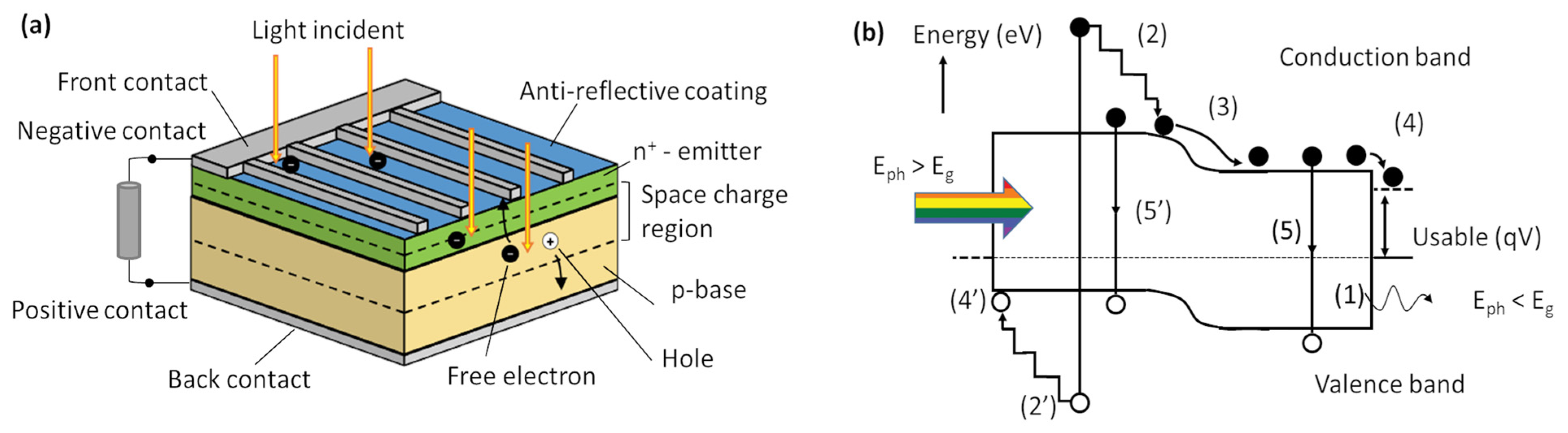
2.1. Silicon-Based Solar Cell

Silicon is one of the most abundant materials on the earth and is part of the first generation of solar cells where the semiconductor material is characterized by a high value of the diffusion length and low recombination rate (especially for monocrystalline structure) [37]. These properties can be related to its indirect energy band gap of 1.1 eV, which makes the radiative recombination fairly inefficient, implying that, for defect-free material, the photogenerated electrons and holes can exhibit very long lifetimes [38]. However, due to its relatively low light absorption coefficient, particularly near its band gap (for a comparison of the absorption coefficients of several photovoltaic materials see [39]), the silicon solar cells require comparatively thicker silicon wafers to absorb incoming sunlight sufficiently (~160–350 μm) [40]. In 2022, an optimum silicon solar cell with light trapping and very good surface passivation was about 160 µm thick [41].
Apart from silicon, another interesting semiconductor material is gallium arsenide (GaAs), which is used to fabricate the most performant single-junction device. Being that Ga and As are scarce materials in the Earth’s crust, GaAs solar cells are considered as a replacement for silicon solar cells mostly in the aerospace field, where higher cell efficiency, good tolerance to temperature stress, and better radiation resistance are needed, while cost considerations are less important [42,43]. Due to their limited diffusion, this type of solar cell will not be further discussed.
The typical structure of a solar cell is based on a homojunction of single-crystal material (e.g., Si or GaAs) doped with different species to form a p–n junction. This is typically achieved through diffusion or implantation of specific impurities (dopants) or via a deposition process [44]. In Figure 2a, the cross-section of a conventional silicon solar cell with the basic operation is shown. Sunlight is incident from the top of the solar cell and the metallic grid forms one of the electrical contacts of the diode. An anti-reflective coating between the grid lines increases the amount of light transmitted to the semiconductor by lowering the reflection. The metallic layer on the back of the solar cell forms the other electrical contact of the diode.
Under illumination, the light absorbed by the semiconductor generates electric charge carriers called electrons and holes. These photogenerated carriers present in the space-charge region are separated by the electric field (at the interface of the p–n junction). The electrons diffuse to the n-side and the holes diffuse to the p-side, becoming the majority carriers. This mechanism reduces the probability of undesired recombinations within the device, especially for defect-free wafers (e.g., monocrystalline) where the effects of impurities, grain boundaries, and dislocations are negligible [37].
In order to achieve a high-efficiency cell, several improvements (e.g., buried contact or the presence of a dielectric passivation layer on the rear side) have been implemented to reduce the optical and electrical losses. For instance, these performant structures are texturized at the bottom for light trapping, there is the presence of n++ regions for preventing the Schottky contact on the front, and a p+-layer is used for forming the back surface field at the bottom [38,40]. In the past decade, amorphous-silicon/crystalline-silicon (a-Si/c-Si) heterojunction solar cells have reached record high efficiencies over 26% and are an important device for research in the community [19,45]. Here, the a-Si layers act as very effective passivating layers for the c-Si wafer cell, resulting in an open circuit voltage of more than 700 mV. Moreover, the use of interdigitated back contact technology and temperature below 200 °C for the deposition of a-Si have promoted the diffusion of this solar cell type [45,46].
As reported in Figure 1, the light-to-electrical power conversion efficiency η of a silicon-based single junction solar cell ranges between 25.0 and 26.1% depending on several factors, out of which the doping of the base material is one [19,47]. This value is slightly lower than the theoretical value determined by the Shockley–Queisser model (that is 30% for an energy bang gap of 1.1 eV) [48]. The difference in terms of the η values is related to the loss mechanisms within the device. Figure 2b shows the main loss mechanisms in a standard p–n junction solar cell with E g as the forbidden band gap energy of the semiconductor material [44,49]. Here, the most significant losses are the non-absorption of below-bandgap photons ( E p h < E g (1) in Figure 2b) and thermalization of electron–hole pairs generated by the absorption of short wavelength photons through electron (hole) relaxation to the conduction (valence) band edge ((2) in Figure 2b). The other losses are junction loss ((3) in Figure 2b) and contact loss ((4) in Figure 2b), which can be arbitrarily small in an ideal device.
The recombination losses ((5) in Figure 2b) occur in the device when the theoretically ideal crystal is impure due to foreign atoms, crystal structure errors, or similar issues. In this case, the forbidden gap contains additional energy levels that work as recombination centers, also called traps. Besides foreign atoms, crystal imperfections, such as empty lattice places or crystal displacements, also lead to increased recombination. Here, the crystal quality of the semiconductor layers impacts the solar cell performance, influencing the carrier lifetime τ n . Its value lies in the range from ms down to μs [37]. Another useful parameter is the electron diffusion length L n , which describes the distance a generated electron moves in the semiconductor in the absence of an electric field, until it recombines. The typical numerical values for silicon, for instance, are between 50 and 500 μm [37].

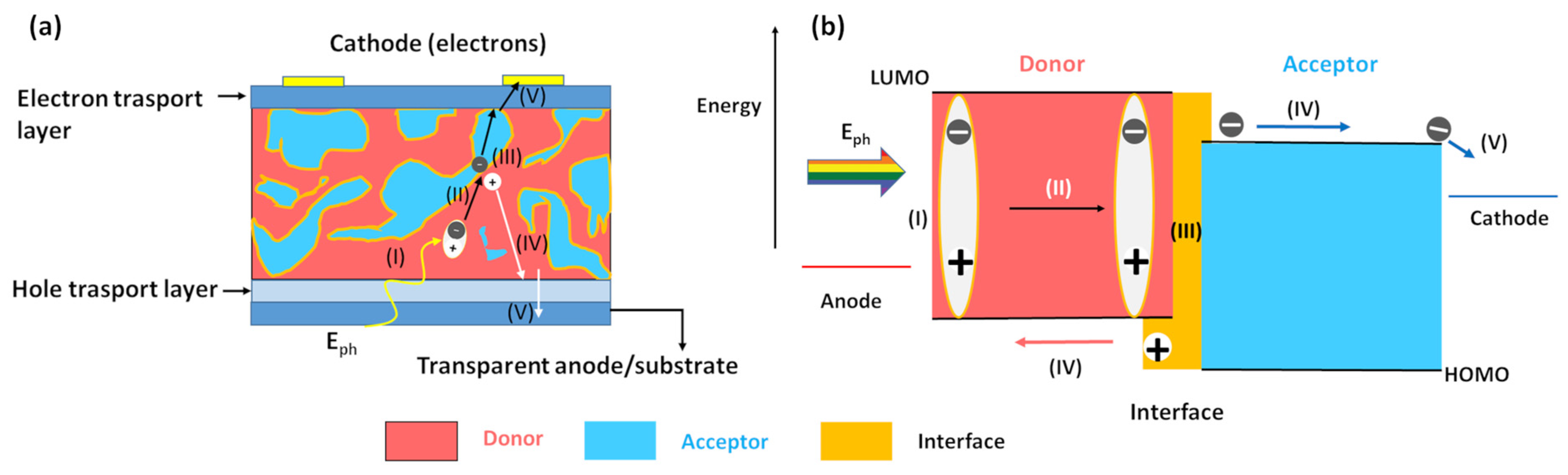
2.2. Polymer: Fullerene-Based Solar Cell

In 1986, Tang et al. reported the first organic solar cell based on the donor–acceptor concept in a bilayer structure [50]. It is worth noting that solar cells based on organic materials had already been reported in the late 1970s, although with very poor conversion efficiencies. For a review of these early organic photovoltaics, the reader is referred to the work of Chamberlain et al. in 1983 [51].
In the 1990s, the introduction of the bulk heterojunction concept by Heeger and Friend allowed for enhancing the device efficiency [52,53]. In particular, they fabricated the first devices based on blending the conjugated semiconducting polymer with C60 or its functionalized derivatives.
Beginning in 1995, the polymer photovoltaic cells started to improve, reaching a power conversion efficiency value of 2.5% in 2001, as reported by Shaheen et al. [54]. Subsequently, by using a different combination of donor–acceptor materials based on low band gap polymers, the η value exceeded 10% for laboratory devices with an active area of ∼1 cm2 [14,55,56]. In the last few years, the use of new blends based on a ternary compound and non-fullerene additives has led to a further enhancement of solar cell performance. In Figure 1, the development of the power conversion efficiency of organic solar cells is summarized. As can be noted, the η of a 1 cm2 OPV device reached a certified value of 15.2% using D18 as the electron donor and Y6 as an acceptor in a single junction non-fullerene polymer solar [19,57]. More recently, for a small area (0.032 cm2) organic solar cell, a NREL-certified efficiency of 18.2% has been reported [19,20].
Differently from the inorganic semiconductors (e.g., Si, GaAs, etc.), the absorption of a photon in the OPV creates an exciton (i.e., a bound electron–hole pair) with binding energy (≥0.1 eV) due to the high Coulomb interaction and the reduced size of the system [58]. The exciton must then be split into free carriers (electron and hole separately) before it recombines within the blend, due to its limited diffusion length (~10 nm) [52,53]. This splitting process takes place at the interface between the donor (p-type) and the acceptor (n-type) organic semiconductors. These materials are chosen such that an energy difference between the respective molecular energy levels (that are HOMO and LUMO) exist to dissociate the photo-generated excitons at the donor/acceptor interface. Here, LUMO stands for the lowest unoccupied molecular orbital for the electrons in the acceptor, and HOMO refers to the highest occupied molecular orbital for the holes in the donor.
In Figure 3a, a simplified sketch of a typical heterojunction structure for an OPV device is depicted. As can be seen, the active layer consists of an intermixing of the donor and acceptor materials so that a fine interpenetrating network builds up with extended donor–acceptor interfaces distributed within the bulk. In Figure 3b, the main steps occurring within the organic active layer for (I) the generation of an exciton via photon absorption, (II) diffusion, (III) splitting at the interface between the donor and acceptor, and (IV) charge carrier transport for (V) collection at the metal contacts are shown [8]. Here, the principal loss mechanism involves the breaking up of the exciton and the subsequent charge carrier collection [59]. Optimizing the blend morphology by changing the preparation conditions (e.g., deposition temperature and solvent additives) is, therefore, necessary to reduce the recombination kinetics [60].

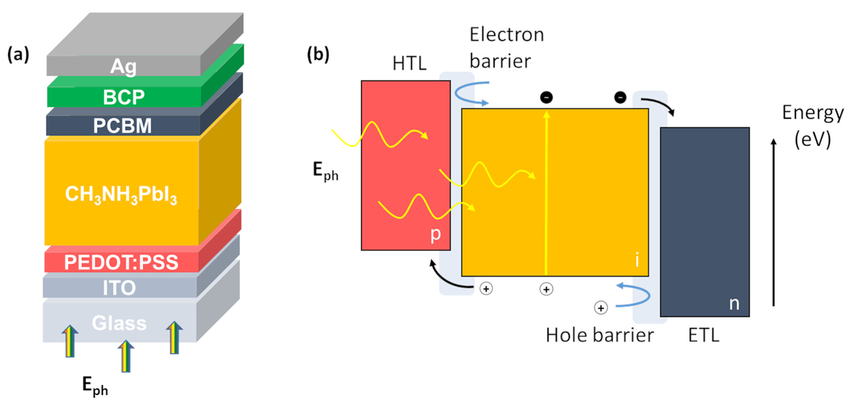
2.3. Perovskite-Based Solar Cell

Perovskite-based solar cells are a new entry within thin film PV technologies and they have a good chance of contributing to large-scale solar energy production thanks to their high η value and compatibility with scalable processes [31]. The first investigated Perovskite was a calcium titanium oxide mineral (CaTiO3) discovered by the Prussian mineralogist G. Rose in 1839. This type of compound has a chemical structure ABX3, where “A” and “B” are two cations of very different sizes and “X“ is a halogen anion (usually I, Br, Cl, or a combination of these) that binds to both [61]. The first type of perovskite material used for PV applications has been an alkali halide type (CH3NH3PbI3), where “A” is usually methylammonium (MA) [62], but, lately, can be formamidinium (FA) [63], cesium [64], and rubidium [65]; and “B” is a metal (Pb, Sn, Sr) [61].
The first photovoltaic cell based on perovskite was published in 2009 with an efficiency of about 3.8%, comparable with the organic devices [66]. Here, the evidence of the photovoltaic function for perovskite nanocrystalline particles self-organized on TiO2 as n-type semiconductors has been reported. In less than two decades, the efficiency increased, reaching the NREL-certified η value of 25.7% [19,67]. These excellent device performances are due to their efficient and balanced ambipolar transport property (high carrier diffusion length in a range of 0.1–1μm depending on the halide) and strong absorption coefficient on the order of 104 cm−1. Moreover, the ability to tune the bandgap value by changing the composition permits us to use the perovskite for a broad range of optoelectronic devices, such as light-emitting diodes [68], photo-detectors [69,70], lasers [71], and tandem solar cells [19,72,73]. Recently, efficient monolithic perovskite/silicon and perovskite/CIGS tandem solar cells have been fabricated at low temperatures with η values of 31.2% (see Figure 1) and 24.2%, respectively [19]. Again, these type of thin-film perovskite tandem cells show high proton radiation hardness properties with a mitigation of the defects induced by the radiation [72,73].
The typical structure of a perovskite solar cell is a p–i–n junction device, where the perovskite has the role of an intrinsic (i) sunlight absorber [74]. Here, the n-type electron transporting layer or material (ETL-M) and a p-type hole transporting layer (HTL-M) are employed to separate and collect the photogenerated charges. In Figure 4a, the cross-section of the device with phenyl-C61-butyric acid methyl ester (PCBM) as the electron-transporting (n-type) material and PEDOT:PSS (poly(3,4-ethylenedioxythiophene):poly(styrenesulfonate) as the hole-transporting (p-type) material is shown. Usually used as a photoanode, a transparent conductive oxide (TCO), e.g., fluorine-doped tin oxide (FTO) or indium-doped tin oxide (ITO), is used, whereas the counter electrode, typically made of Pt, Au, and Ag in more recent years, is made of cheaper conductive materials, e.g., carbon [75]. To enhance the long-term stability, a bathocuproine (BCP) buffer layer has been commonly used in p–i–n perovskite solar [76]. Similar to other PV technologies, the absorption of a photon generated an electron–hole pair with a low value of binding energy that induces exciton dissociation at room temperature and, consequently, the charges move freely across the layer [77]. In Figure 4b, a schematic energy-level diagram of perovskite materials with electron (n-type)/hole (p-type) transporting materials is reported.
Vacuum evaporation is considered a high-performance technique to grow oriented thin films of layered perovskite with precise control of the film properties, compared to the deposition through spin-coating and blade coating followed by thermal annealing [62]. This latter step allows for solvent evaporation and enhances perovskite crystallization [78]. However, the perovskite-based devices are characterized by poor long-term stability and by some toxicity issues related to the presence of lead compounds [79] and the use of solvents, such as N,N-dimethylformamide (DMF), dimethyl sulfoxide (DMSO), γ-butyrolactone (GBL), and toluene, for the fabrication processes [80].
In the literature, several approaches have been proposed to optimize the homogeneity, morphology, and grain-size dimension of the perovskite layer. This leads to a mitigation of the recombination processes through defect states on the device performance [81,82]. In this respect, Chen et al. have reported that using chlorine as an extrinsic dopant during the solution crystallization and grain growth of CH3NH3PbI3 produces an enhancement of the film quality, which results in improved efficiency [81]. The most performant large-area module obtained by connecting 55 perovskite cells shows an initial efficiency value of 17.9% [19,83]. Han et al. have tested the stability of similar devices under different environmental conditions (temperature, humidity, and light illumination), evidencing ageing phenomena affecting the perovskite material and the whole solar cell (e.g., crystal structure, film quality, conducting layers and interfaces) [84]. Here, long-term stability is still an issue to resolve. The performing standard, as well as alternative experimental measurements, will systematically help to improve the stability of these devices in the future [85].

2.4. Solar Cell Characterization Techniques

For the emerging photovoltaic technologies based on organic semiconductors, quantum dots, hybrid materials, and perovskites, an accurate characterization becomes necessary for material screening and device optimization. In the literature, several electrical and optical characterization techniques, such as light-induced charge extraction by linearly increasing voltage (CELIV), impedance spectroscopy (IS), transient photovoltage (TPV), photoluminescence (PL) decay, electroluminescence (EL), and transient microwave reflection (TRMC), have been reported to extract significant solar cell parameters (e.g., charge carrier mobility and lifetime, charge density, the density of traps and their energy depth, and more) [60,72,86,87,88,89]. The latter technique has also been shown to enable an in-situ characterization of the electronic heterojunction interfaces’ properties during their formation [90]. More recently, the PL and EL techniques have been applied to understand and minimize the open circuit voltage losses in all-perovskite tandem photovoltaics [91].
By considering the silicon-based devices, where the total thickness of the emitter (n+) and base (p) layers ranges between 160 and 350 μm, the charge transport is governed by the diffusion of minority carriers within the doped regions. Therefore, the quality of crystalline silicon determines the minority carrier lifetime and diffusion length within the structure, which influences the solar cell performance. As reported in Figure 1, monocrystalline silicon solar cells characterized by a perfect lattice structure, high material purity, and low dislocation density (single crystal-like) show higher η values compared to the same structures with polycrystalline silicon.
On the other hand, the organic and perovskite thin film solar cells (denoted also as hybrid and organic photovoltaics) are 50 and 300 nm thick, respectively, and are comprised of a p–i–n junction [32,92]. It is worth noting that the BHJ can also be considered p–i–n-structured, being that the polymer is undoped. The use of electrodes with different work functions and doped injection layers (ETL and HTL) creates a built-in potential that drops inside the intrinsic region.
The electron and hole densities vary spatially within the intrinsic region and there are no minority carriers, as observed in the bulk of the crystalline silicon. It is worth noting that the perovskite material and the organic semiconductor are characterized by ambipolar charge transport properties [74,93]. Quantifying a diffusion length in a p–i–n-structured solar cell is, therefore, less significant for the emerging material [87]. The characterization of the charge transport in p–i–n structures requires the measurement of the electron and hole mobilities, the recombination coefficient, the built-in potential, charge injection barriers, and other parameters associated with charge trapping. However, it is difficult to assess these parameters individually, as they are highly entangled in a solar cell device.
Here, the morphology properties of the intrinsic layer (perovskite or donor–acceptor blend) depend on the preparation conditions, such as solvent additives, interface layers (e.g., LiF and C60 for perovskites), thermal treatment, and substrate [82,93,94]. For example in polymer:fullerene solar cells, the use of high-boiling point solvent additives increases the mesoscopic order and crystallinity within the active layer, and induces clear improvements in the charge carrier transport [93]. Shao et al. have demonstrated that the use of the fullerene material as ETL leads to a partial deactivation of the surface and of the grain boundary charge traps, related to the perovskite absorber layer. This also helps to eliminate the often observed photocurrent hysteresis and to increase the charge carrier lifetime and mobility [82]. In particular, Warby et al. report that the performance of single-junction cells is largely limited by significant nonradiative recombination at the perovskite/organic electron transport layer junctions [94]. This is especially true for monolithically-stacked structures (e.g., perovskite/silicon, perovskite/CIGS and perovskite/perovskite tandem devices), where the higher performance can be reached only by optimizing the recombination phenomena at the interfaces [91].
Additionally, both the emerging materials suffer from degradation phenomena (induced by the light soaking, thermal stress, and environmental moisture) that originates a charged defect at the interface and within the bulk material, which modifies the charge carrier dynamics. As a consequence, the recombination and transport of charges are more difficult to understand and require more sensitive characterization techniques.
At present, few characterization techniques can detect material modifications that affect the interface, doping, and electron/hole transport within the complex structure of the solar cells (multi-layers stack plus electrodes) under operating conditions. The noise spectra unravel the dynamics of very specific electronic processes that occur at the interfaces and within the bulk material, where other conventional structural/morphological and chemical characterization techniques (e.g., near-UV photoelectron spectroscopy [95], surface photo-voltage measurements [96], real-time spectroscopic ellipsometry [97], and Fourier transform infrared spectroscopy (FTIR) [98]) are less sensitive. These latter techniques need to be accompanied by complementary measurements that can provide additional information regarding the electronic transport of the material [13].
Recently, noise spectroscopy has proved to be a powerful and non-destructive tool for the analysis of electric transport, recombination, and degradation phenomena in solar cell devices [13,32,93,99,100,101]. Degradation phenomena at the interfaces and within the bulk material (based on Czochralski-grown silicon, organic and perovskite compounds) induced by an interstitial boron–oxygen complex defect [101], thermal stress [13,99], and proton radiation [101] have been characterized in detail. Here, the noise amplitude is correlated with the device performance. Morphological modifications originated from the solvent additives [100], phase transition [102], and grain boundary dimensions [32] have been investigated using charge carrier fluctuation measurements. Useful parameters, such as the density of states (DOS), electron lifetime, charge carrier mobility, and complete electronic characterization of the defect states (e.g., defect density, energy depth, and symmetric ratio) have been computed [32,93,99,100,101]. Moreover, the noise analysis reveals that, within the perovskite-based devices, the recombination kinetics is strongly influenced by the electron–phonon interactions [32].
Among the electrical measurement techniques, impedance spectroscopy can be considered an equivalent tool for the characterization, analysis, and diagnosis of solar cells compared to noise spectroscopy [103]. In this respect, several authors report a comparison between the noise and impedance spectra by correlating the experimental quantities with the physical parameters of the investigated devices [104,105]. Both techniques operate in the same frequency range, which is 1 Hz–100 kHz. The measurements at low frequency can be investigated for the electrode polarization, ions, and charge accumulation at the interface and within the bulk [106]. These phenomena are well-reported in the literature, for the perovskite-based solar cell, where mixed ionic–electronic conduction mechanisms have been observed [107]. Conversely at high frequencies, these techniques are sensitive to recombination processes and trapping/detrapping phenomena. For the emerging PV devices, the timescales of the dynamics lie in the frequency range taken into account. It is worth noting that impedance spectroscopy can also acquire spectra at frequencies below 1 Hz and above 100 kHz for energy storage and solid-state semiconductor devices applications, respectively [108,109,110,111,112,113,114,115]. Similar to the impedance measurements, with the analysis of the fluctuations, the information can be extracted and quantified from the noise spectrum by using an AC-equivalent circuit [13,101,103]. Here, the corresponding parameters give insights into the underlying physical nature of the different processes within the investigated device.
To perform the noise spectra measurement, the device is biased with a low-noise DC current in the μA range. The output AC voltage signal is amplified with a low-noise preamplifier and, subsequently, fast-acquired (in one shot in 2 min) with a spectrum analyzer. Conversely, the impedance measurement requires a voltage small-signal sinusoidal electrical input (orders of tens mV) superimposed on the applied DC voltage. The AC voltage excitation changes within the investigated range as a function of the frequency, depending on the measurements, and the resulting impedance is acquired. For the latter case, the acquisition time, especially at lower frequencies with adequate averaging and with a sufficient number of points for decades, leads to a longer measurement time (orders of ten minutes). Moreover, the noise spectra are acquired at different bias points under the current-controlled operation mode (galvanostatic mode) with a small excitation amplitude that varies in a range of μA. This ensures that the degradation phenomena caused by the bias current within the investigated devices are limited [116].
The low-frequency noise signal becomes prominent in small devices with sub-micron dimensions following a 1 / V o l u m e scaling factor [117]. This trend has been observed for the downscaled silicon transistors, where an increase in the relative level of low-frequency noise becomes a limiting factor for advanced electronic applications [118] and solar cells [101]. For the PV devices, one of the dimensions is almost fixed by the vertical layout (e.g., thickness of the emitter-base junction or injection and intrinsic layers). Therefore, active area A plays an important role in the noise analysis. It is worth noting that the most performant devices based on emerging materials on a laboratory scale are characterized by a small area below 1 cm2 [19,20,57]. With an increase of the device area, the recombination kinetics become more important and negatively affect the overall performance. Since the noise fluctuations are amplified within thin devices with a small area, as for the organic and perovskite PV cells, this feature makes the noise spectroscopy more sensitive and effective compared to the other characterization and diagnostic tools.
Within the solar cells with a planar multi-layered structure, the intrinsic layer and interfaces are the most resistive elements of the pile and produce more significant noise contributions [119,120]. This proves that noise spectroscopy, compared to conventional electrical techniques, provides more space selectivity of the processes involved by identifying and characterizing the performance-limiting sources within the devices. In Figure 5, the advantages, features, and practical aspects of the use of noise spectroscopy tool are summarized.

3. Electric Noise Spectroscopy: General Concepts and Measurement Techniques

By definition, a random process is a random function x ( t ) of an independent variable t , which, in the theory of fluctuations, is the time. The deviation of the random quantity x ( t ) from its mean value x is called fluctuation, or noise, defined as [121]:
δ x t = x t x
The evolution of δ x t in time on average is analyzed through the correlation function, calculated as [122]:
δ x t 1 δ x t n = d x 1 d x 2 d x n δ x 1 δ x n w n x 1 , t 1 ; ; x n , t n
where x i are the values of the random quantity at instants t i (i = 1, …, n), and the probability density function w n is known for the different instants t 1 , , t n .
The kinetics of the random fluctuations can be described very precisely when w n is of Gaussian-type. In the case of random processes composed by Gaussian processes, the correlation function establishes the correlation between the values of the random process at two different times t 1 and t 2 . Therefore, Equation (2) can be rewritten as:
Ψ x t 1 , t 2 = d x 1 d x 2 δ x 1 δ x 2 w 2 x 1 , t 1 ; x 2 , t 2
with w 2 as the two-dimensional probability density. In Equation (3), Ψ x t 1 , t 2 is commonly known as the autocorrelation function, only depending on the difference t 1 t 2 in the case of stationary systems [123].
While in the time domain, the basic properties of random data can be obtained by this autocorrelation function, in the frequency domain, instead, similar information can be given by the spectral density function S x ( f ) defined, according to the Wiener–Khinchin theorem [124,125], as:
S x ( f ) = + d t 1 t 2 e i ω t 1 t 2 Ψ x t 1 t 2 Ψ x ω
From Equation (4), it follows that S x is the Fourier transform of Ψ x and, consequently, the integral S x over all positive frequencies is exactly the variance of the noise (i.e., the amplitude of the fluctuations) [121].
It is well-known that in any condensed matter system, the frequency dependence of the spectral density and the response of the same system to external perturbation (the electric current transport) are governed by the same kinetic processes. Therefore, one can expect that there is a relationship between the two kinetic characteristics of the system [122]. For example, in metals, some of the defects are mobile. The hopping motion of the scattering centers changes their arrangement and affects the resistance, producing the resistance fluctuation phenomenon. In semiconductors, the states of electrons and holes can be divided into two classes: delocalized electron states in the conduction band (holes in the valence band) and localized states. The transition of an electron or a hole from a localized to a delocalized one is called generation and the inverse process is called recombination. Since the elementary generation and recombination processes are random, the number of charge carriers fluctuates around some mean value. These fluctuations of the charge carriers number produce fluctuations of the resistance and, consequently, of the current and/or voltage if a nonzero mean current is passing through the specimen. All these important relationships to the basic characteristics of the physical system involved can be obtained by analyzing the frequency components of the spectral density function, from which it is possible to identify four common types of low-frequency noise [121].
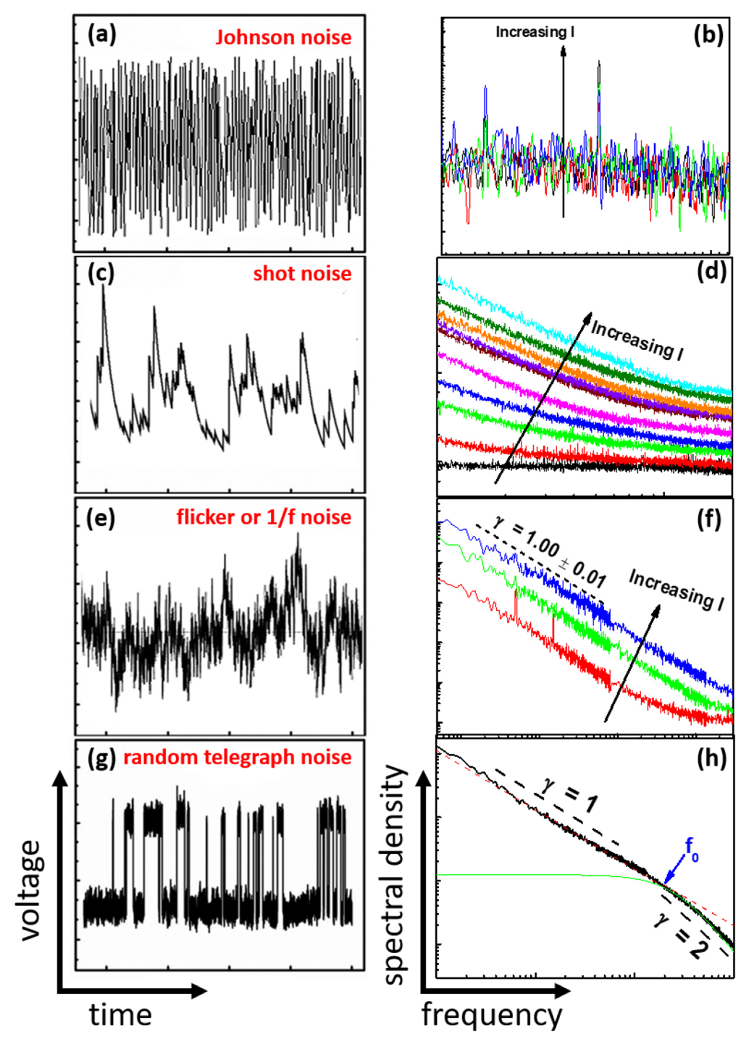
  • The electronic noise generated by the thermal agitation of the charge carriers (usually electrons) inside an electrical conductor at equilibrium is the Johnson or thermal noise (Figure 6a). These temperature fluctuation processes are also known as “white noise”, having a voltage-spectral density completely frequency-independent (Figure 6b) and expressed by the following expression:
    S V ( f ) = 4 k B T R
    where k B is the Boltzmann constant, T is the system temperature, and R is the real part of the system impedance [121,126].
  • The electronic noise, which can be modeled by a Poisson process and is originated from the discrete nature of electric charge, is the shot noise (Figure 6c). Similar to temperature fluctuations, current fluctuation processes are also identified as “white noise”, having a voltage-spectral density defined as:
    S V ( f ) = 2 e R D 2 I
    where e is the electron charge, R D is the differential resistance of the system, and I is the bias current [121,127]. In Figure 6d, the linear current dependence of the shot noise amplitude is shown.
  • The electronic noise generated by slow random dynamics is usually known as 1/ f or flicker noise (Figure 6e). This is characterized by a frequency spectrum which is inversely proportional to the frequency of the signal (Figure 6f), and is modeled through the Hooge empirical relation as:
    S V ( f ) = α H n V 2 Ω 1 f γ
    where V is the dc voltage ( V = R I in the case of Ohmic compounds), f is the frequency, α H / n is the normalized Hooge parameter proportional to the noise level amplitude (being n the charge carrier density), and γ is the frequency exponent assuming values in the range from 0.8 to 1.2 [117,121,128].
  • The electronic noise consisting of sudden step-like transitions between two or more discrete voltage or current levels (Figure 6g) is the random telegraph noise (RTN). RTN has a spectral density expressed by a Lorentzian type of noise as:
    S V ( f ) = L n a f 0 1 + f f 0 2
    where L n a is the Lorentzian noise amplitude and f 0 is a cutoff frequency representing the crossover value of the transition from a 1/ f to a 1/ f 2 behavior (see Figure 6h for details) [121,129].
Concerning the measurement of the voltage-noise fluctuations, all the acquisition is concentrated on the AC component of the output signal. This is preamplified with homemade electronics or with a Signal Recovery model 5113 low-noise preamplifier and is analyzed with a dynamic signal analyzer, Hewlett-Packard model HP35670A. A schematic picture of the setup used to perform the noise spectra is shown in Figure 7.
The system temperature, which is one of the most important external parameters to be controlled during the noise spectral traces recording, is varied with a closed-cycle cold finger refrigerator, operating in a range between 300 and 8 K, or with a series of thermoelectric Peltier-type devices, operating in a range between 350 and 240 K. In each case, a proportional–integral-derivative (PID) algorithm is used for the temperature stabilization, better than 0.2 K. The electrical connections to the samples under test are realized in a four-probe contact configuration. This technique, which is the most common way to measure the DC electric transport properties, does not completely eliminate the external spurious and unwanted contributions in noise studies alone. In this case, indeed, additional current fluctuations can be produced by the noise of each component constituting the bias and measurement circuit. In principle, this problem could be partially solved with the use of an ideal current source, whose effect is to reduce current contact resistance fluctuations [130]. However, electronic feedback circuits act as ideal sources at DC, but do not always work in AC. Therefore, it is clear that high-quality voltage-spectral density measurements can be performed only by developing an experimental procedure able to separate and subtract noise components due to contact resistance fluctuations and active instrumentation of the experimental setup (“background noise”). This has already been realized by resorting to a specific analytical correction based on a sequence of two- and four-probe measurements, followed by a mathematical manipulation of the data [131,132,133]. The validity of the entire procedure has been verified several times on different condensed matter systems and devices, such as ultrathin films for green [134], superconducting [135] and magnetic [136] electronic applications, and superconducting nanowires [137,138] and thin film structures [139,140].

4. Physical Phenomena and Fluctuation Mechanisms in Solar Cells

In this section, the physical models, the effect of different agents on cell performances, DC transport and voltage-noise analysis of solar cells realized with different technologies are reported. The results obtained by the authors with the experimental investigations are described, respectively, for:
  • Silicon-based cells (see Figure 2a for a schematic representation). The model of fluctuations, the effect of radiation damage, and evidence of damage from noise are the topics of Section 4.1.
  • Organic cells (see Figure 3a for a schematic representation). Physical modeling through the noise, effects of fabrication technology on cell parameters through the noise, and thermal stress effects characterized by noise are the topics of Section 4.2.
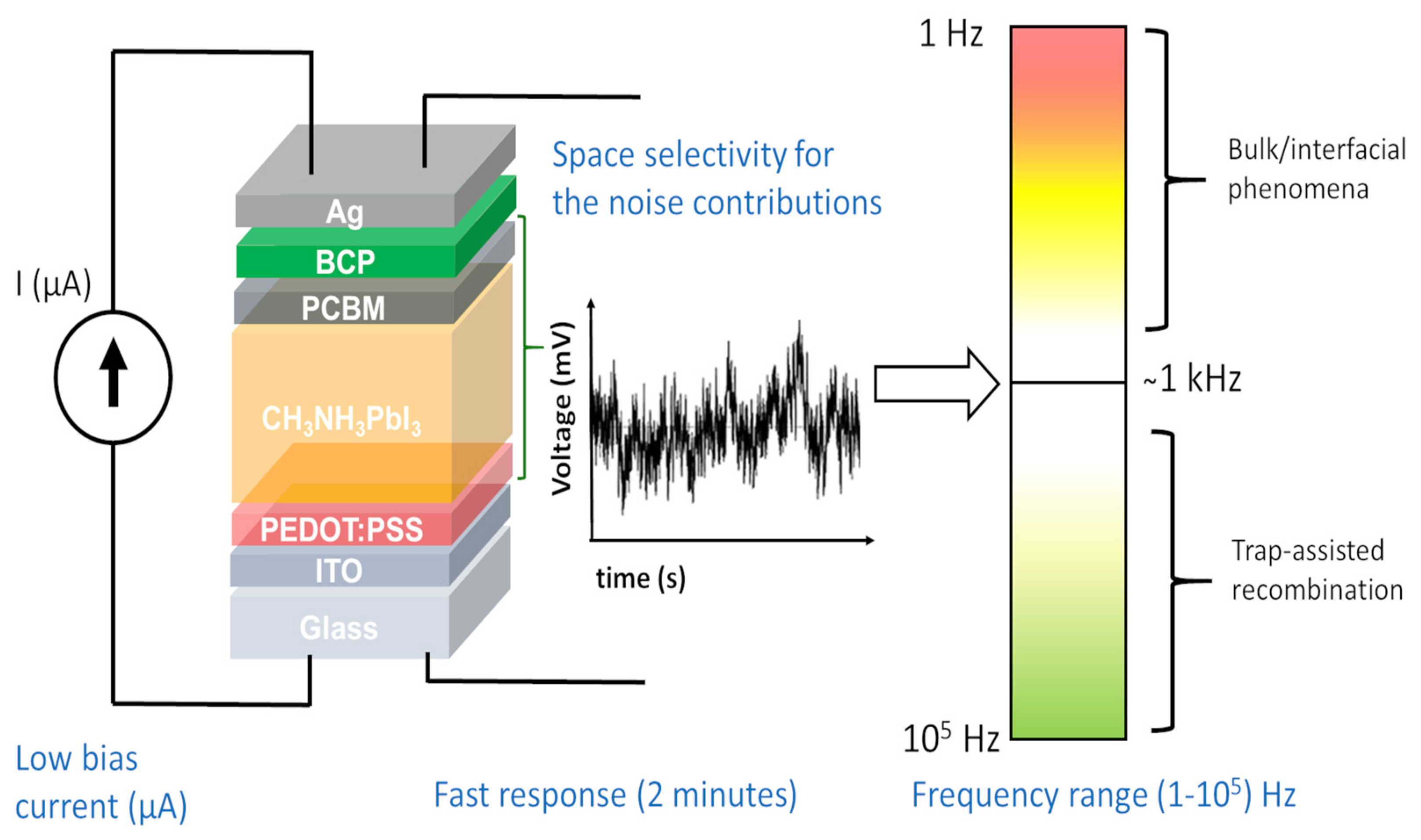
  • Perovskite-based cells (see Figure 4a for a schematic representation). Physical modeling through the noise, material characterization through the noise, and the correlation between noise and cell efficiency are the topics of Section 4.3.

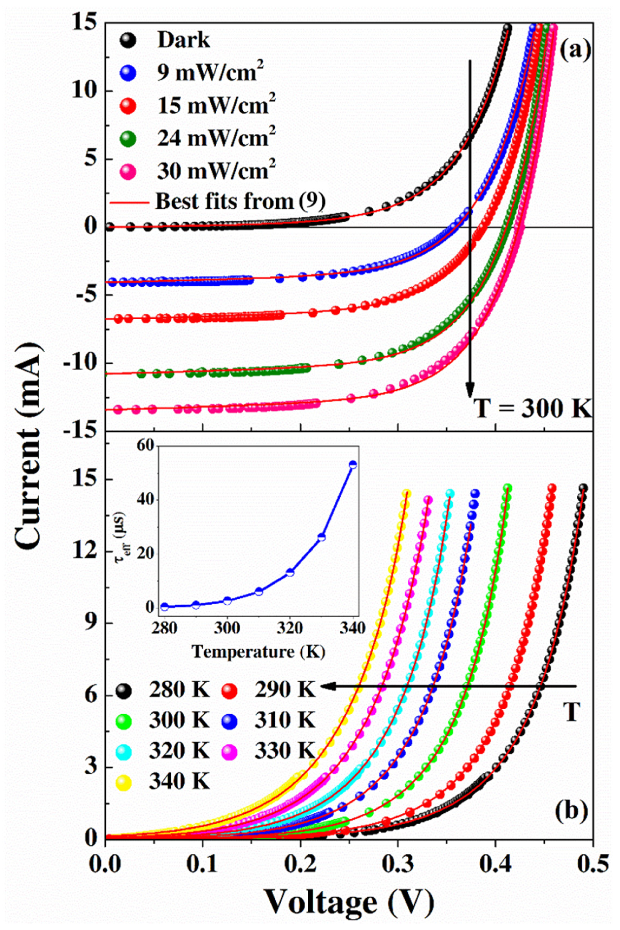
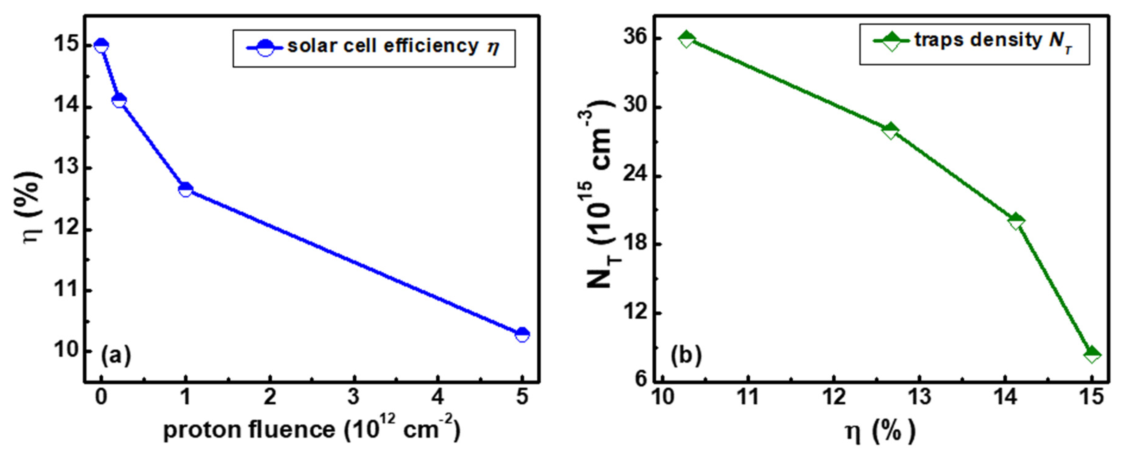
4.1. Photocurrent Fluctuation Effects in Polycrystalline Silicon-Based Solar Cells

Spectra from 1/ f -type noise have often been observed in semiconductors and p–n junctions, and several works have been addressed to understand the origin of this behavior [121,141,142,143,144,145]. Semi-empirical models have been proposed to relate the current noise to mobility fluctuations [142], to the fluctuation of the number of free charge carriers within the space charge region [143,144] or the semiconductor surface [145]. Hsu [146] and Van der Ziel [147] related the 1/ f -type noise in the metal-oxide semiconductor system and in the p–n junctions to fluctuations of the defect state population. Low-frequency electric noise has also been used to determine the quality of silicon solar cells and photovoltaic modules [148,149,150]. Recently, reliability estimation has been also performed for photovoltaic devices related to microplasma detection [151] and for iron disilicide heterojunction solar cells [152]. More recently, noise spectroscopy has been employed to study the carrier dynamics within silicon homo (p-n junction) and heterojunction (a-Si/c-Si:H heterostructure) solar cells [119,153]. The determination of electronic parameters (such as energy level, density, and symmetric ratio) of defect states within the forbidden bandgap allows for the estimation of their influence on the electronic performance of the semiconductor devices [154,155,156]. Dedicated measurement techniques, such as injection-dependent lifetime spectroscopy [157], temperature-dependent lifetime spectroscopy [157], thermal admittance spectroscopy [158,159], and deep-level transient spectroscopy [160,161], are commonly used to determine the detailed properties of electronic defects in semiconductors.
In this study, random current fluctuations in Czochralski-type (Cz) crystalline silicon-based homo-junction solar cells, in pristine form and after artificial degradation with high-energy protons, have been measured at different temperatures and illumination levels. The investigated monocrystalline solar cells, type “SC2140-Z8-24”, are based on a homojunction solar cell with a p-type Cz-Si base material and a diffused emitter. They were created by SOLARTEC and the main photoelectric properties are reported in [162]. The samples have an effective area A of 1 cm2 and a wafer thickness d of 320 μm. The traditional theory reproduces the solar cell equivalent circuit into four constituent parts: a photocurrent source, a diode, a series resistor, and a shunt resistor. The photocurrent source is simply the expression of the current due to the optical generation of the charge carriers I p h , the diode represents electron–hole recombination at the p–n junction, the series resistance R s arises from the ohmic contact between the metal and semiconductor internal resistance, and the shunt resistance R s h accounts for the leakage current through the cells [163]. From a mathematical point of view, this framework allows for the modeling of current–voltage I - V as:
I = I 0 e x p e V I R s n k B T 1 + V I R s R s h I p h
where e is the electron charge, k B is the Boltzmann constant, T is the absolute temperature, and I 0 and n are the diode saturation current and ideality factor, respectively [37]. Figure 8a shows the I - V characteristics of the investigated silicon solar cells at 300 K and for different light intensities, ranging from 0 (dark) to 30 mW/cm2. In this respect, a commercial cool white light-emitting diode (LED) “KLC8 Edixeon K series” from Edison Opto was used as light source. The relatively low values of the short-circuit current I s c and of the open-circuit voltage V o c are due to the low light intensity levels used for the electrical characterization. By measuring the same photovoltaic devices under standard test conditions with the AM 1.5 G spectrum, the following parameters have been obtained: I s c = 37.45 mA, V o c = 581 mV, fill factor F F = 68.96%, and a power conversion efficiency η = 15.01% [162]. By fitting the experimental data with Equation (9), the red curves shown in Figure 8a are obtained. A good agreement with the measured data is clearly visible. The estimated series resistance R s is about 1 Ω at 300 K and decreases with the temperature and light intensity. R s h is almost constant in temperature and varies in the range between 2800 Ω and 2100 Ω, going from dark to 30 mW/cm2 illumination.
Figure 8b shows the temperature dependence of the I - V characteristics under dark conditions, measured in the range between 280 and 340 K. The solid red lines are the best-fitting curves obtained by using the model defined with Equation (9). A good agreement with the data points is also evident in this case. The investigated solar cells are based on the n+–p junction and, due to the asymmetric doping concentration, the emitter diffusion current is orders of magnitude lower than the base current. Therefore, it can be assumed that the saturation current related to the diffusion of the electrons into the base is given by:
I 0 e · A · n i 2 · d N A · τ e f f
where n i is the intrinsic carrier concentration of silicon (9.69 × 109 cm−3 at 300 K) [164], N A = 1.4 × 1015 cm−3 is the doping concentration of the base material corresponding to a resistivity of 10 Ω⋅cm [162], and τ e f f is the effective minority carrier lifetime. The values of τ e f f , obtained from Equation (10), are shown in the inset of Figure 8b as a function of the temperature. At 300 K, τ e f f is about 3.2 μs, in good agreement with what was measured in [162] using a different technique.
The DC model, which applies the superposition principle in comparing the dark and illuminated data, can be similarly used to simulate the electric noise of the photovoltaic devices. The low-frequency dependence of the voltage–spectral density, acquired on pristine Si-based solar cells, is shown in Figure 9 at 300 K in dark conditions and at different light intensity values: 6 mW/cm2, 18 mW/cm2, and 30 mW/cm2. Independent from the bias current applied and, as a consequence, from the cell differential resistance R D , a characteristic 1/ f noise component is visible in the form of: S V f ~ K / f γ , with K as the amplitude and the frequency exponent γ 1.18.
As previously defined, starting from Equation (4), the variance of the voltage–noise signal is [121,123]:
V a r V = f m i n f m a x d f · S V = K · f m a x 1 γ f m i n 1 γ 1 γ
where the frequency interval f m i n , f m a x = [1,100,000] Hz is given by the experimental bandwidth. The V a r V is characterized by a quadratic dependence on R D at all illumination and temperature conditions, as shown in Figure 10 at 300 K. This gives a clear indication that the dominant noise sources in the photovoltaic system are current fluctuations, whose amplitude is calculated as: V a r I = V a r V / R D 2 [121].
The origin of these random current fluctuations responsible for the flicker noise must be related to the trapping and to the recombination processes, involving defects in the p-type base material and the charge carriers [142,143,144]. Accordingly, it can be assumed that these mechanisms modulate the number of free carriers, generating noise fluctuations due to the number fluctuations instead of the mobility fluctuations [121]. Moreover, the possibility of selecting different light intensities gives a further opportunity to modulate the density of the trapped minority charge carriers in the solar cell, also influencing the noise amplitude V a r I . It is well-known that trapping and recombination centers are active in solar cells based on p-type boron doped Cz-Si base material, where the charge carrier transport is strongly influenced by the formation of the boron–oxygen-related defect (BO) [165,166].
In this framework, it follows that:
V a r I = V a r I d a r k + V a r I p h
where, under dark conditions, the trapping and recombination processes give origin to a dark background noise V a r I d a r k , which is constant and independent of the bias condition. Meanwhile, by increasing the light intensity, the amplitude of the current fluctuations V a r I p h initially increases by increasing the light intensity and then saturates (see the blue data points in Figure 11 as a function of the generated photocurrent I p h at 300 K). More specifically, the quantity V a r I p h can be expressed in terms of the two contributions, trapping (green curve in Figure 11) and recombination (grey curve in Figure 11), and, therefore, Equation (12) can be rewritten as [101,167]:
V a r I = V a r I d a r k + A 1 · I p h 1 + I p h I 0 l i g h t 2 + A 2 · I p h 1 + I p h I A 2
In Equation (13), I 0 l i g h t allows for the estimation of the threshold photocurrent at which the noise level is almost saturated (see the red curve in Figure 11 for details) and I A takes into account the influence of the cross-section values of the recombination centers, while A 1 and A 2 are the amplitudes of the current fluctuations expressed related to the trapping and recombination mechanisms, respectively [168].
From the best values of the fitting coefficients of Equation (13), it is possible to compute the most important defect states parameters, such as: the density of the trapping centers N T ~ A 1 , the density of the recombination centers N S R H ~ A 2 , the symmetric ratio k ~ 1 / I A , and the energy depth of the traps below the conduction band E N ~ l n 1 / I 0 l i g h t [101]. By measuring the photo-induced noise fluctuations at different temperatures, the defect state’s temperature dependence can be studied. In particular, the orange squares in Figure 12 show that the symmetric ratio k remains constant at a value of about 10.8, up to a temperature of 310 K; after that, a reduction with the increase of the temperature is observed. Moreover, the trap’s energy depth E N is characterized by an average value of ~0.40 eV around 300 K (see the blue circles in Figure 12 for details). These experimental findings are in good agreement with what was observed in the presence of metastable BO defects [154].
Considering that solar cells are usually exposed to various kinds of radiation in a working environment, very comprehensive investigations need to be performed to develop efficient photovoltaic devices able to operate in conditions of increased radiation. In this respect, the sensitive and versatile noise spectroscopy technique could be used for real-time monitoring of solar cell degradation. In order to verify such potentialities, a comparison between non-irradiated and irradiated samples has been carried out by estimating the effect of the damage through the evaluation of the noise parameters. The degradation effects were artificially induced on the devices with proton irradiation, carried out at the ISL of the Hahn-Meitner-Institut in Berlin (Germany), at a proton energy of 65 MeV in air. A homogeneous defect distribution with this energy value has been verified by using a SRIM (Stopping and Range of Ions in Matter) code [169]. The samples were irradiated with three different proton fluences: 2 × 10 11 protons/cm2, 1 × 10 12 protons/cm2, and 5 × 10 12 protons/cm2. Specific information can be found in [162]. It is well known that the internal parameters of solar cells, such as series and parallel resistances, are strongly influenced by external factors [163]. As could be expected, the interaction of radiation with the material produces effective changes in the material itself. In particular, due to the presence of lattice defects, dislocations, and impurities, after silicon is irradiated, both the surface recombination velocity and the density of the surface states are modified [170]. These effects usually lead to a decrease in the photogenerated current density. Degradation of photovoltaic devices, artificially induced by radiation, can be also detected by measurements of the series resistance R s , showing an abrupt increase with proton irradiation. The increase of R s negatively affects other output characteristics of solar cells, such as fill factor and efficiency.
In the presence of radiation, the behavior of the parameters extracted from the DC electric transport investigation can be related to the cell noise level. In particular, from the best fitting procedure achieved by applying Equation (13), it is possible to compute the values of N T for different proton fluences and, therefore, as a function of η . The behavior shown in Figure 13 gives a direct indication of the presence of degradation processes of the photovoltaic device, since the total number of active traps, which contribute to the enhancement of the noise signal, increases with the decrease of the power conversion efficiency. These experimental findings demonstrate that the effect of radiation exposure and the subsequent damage of silicon solar cells can be clearly identified by monitoring the evolution of microscopic parameters extracted from electric noise analysis. Moreover, it is clearly evident that the major disturbance of the structure and of the transport mechanisms that leads to a noise enhancement occurs at the beginning of radiation exposure.

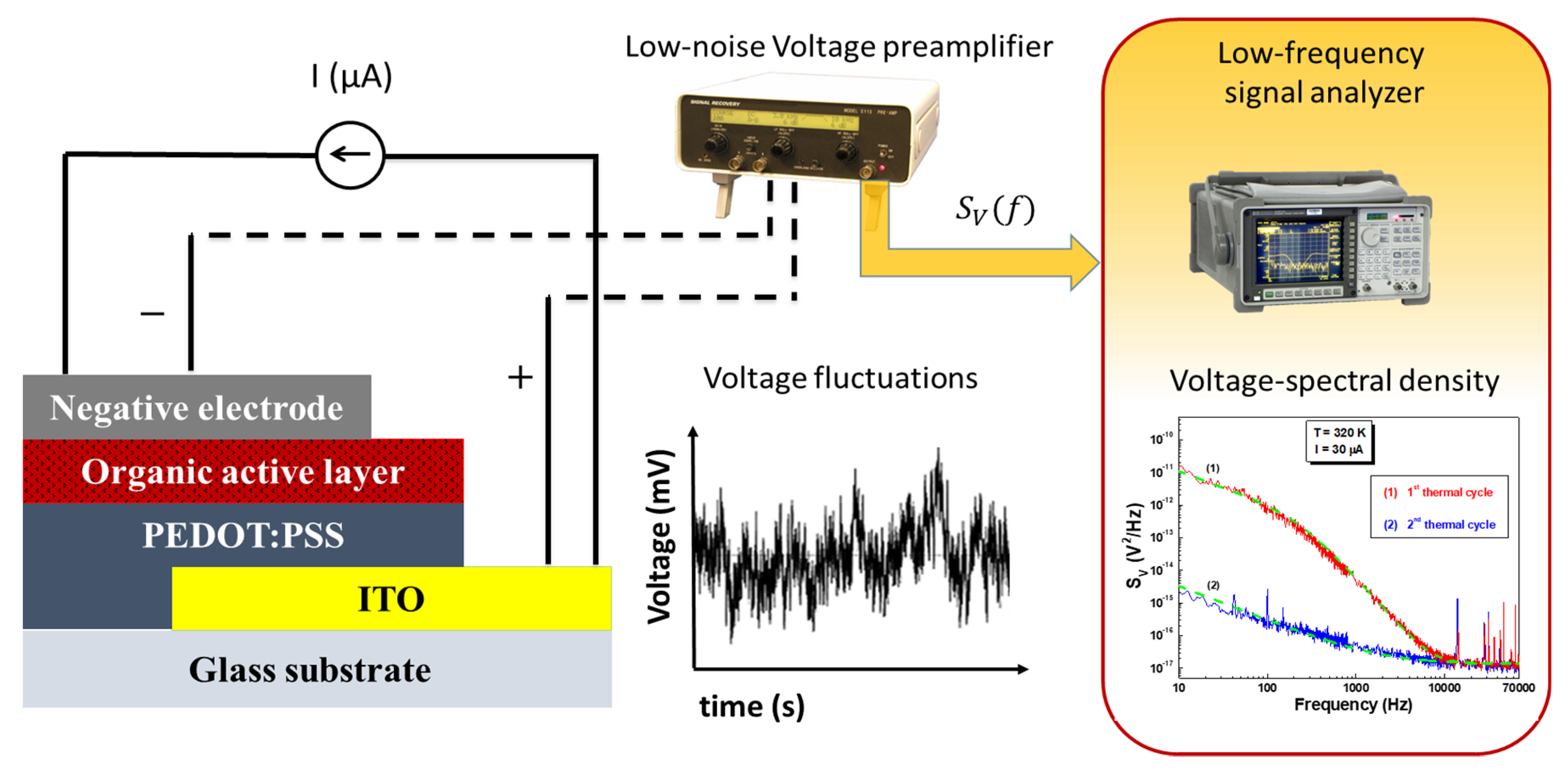
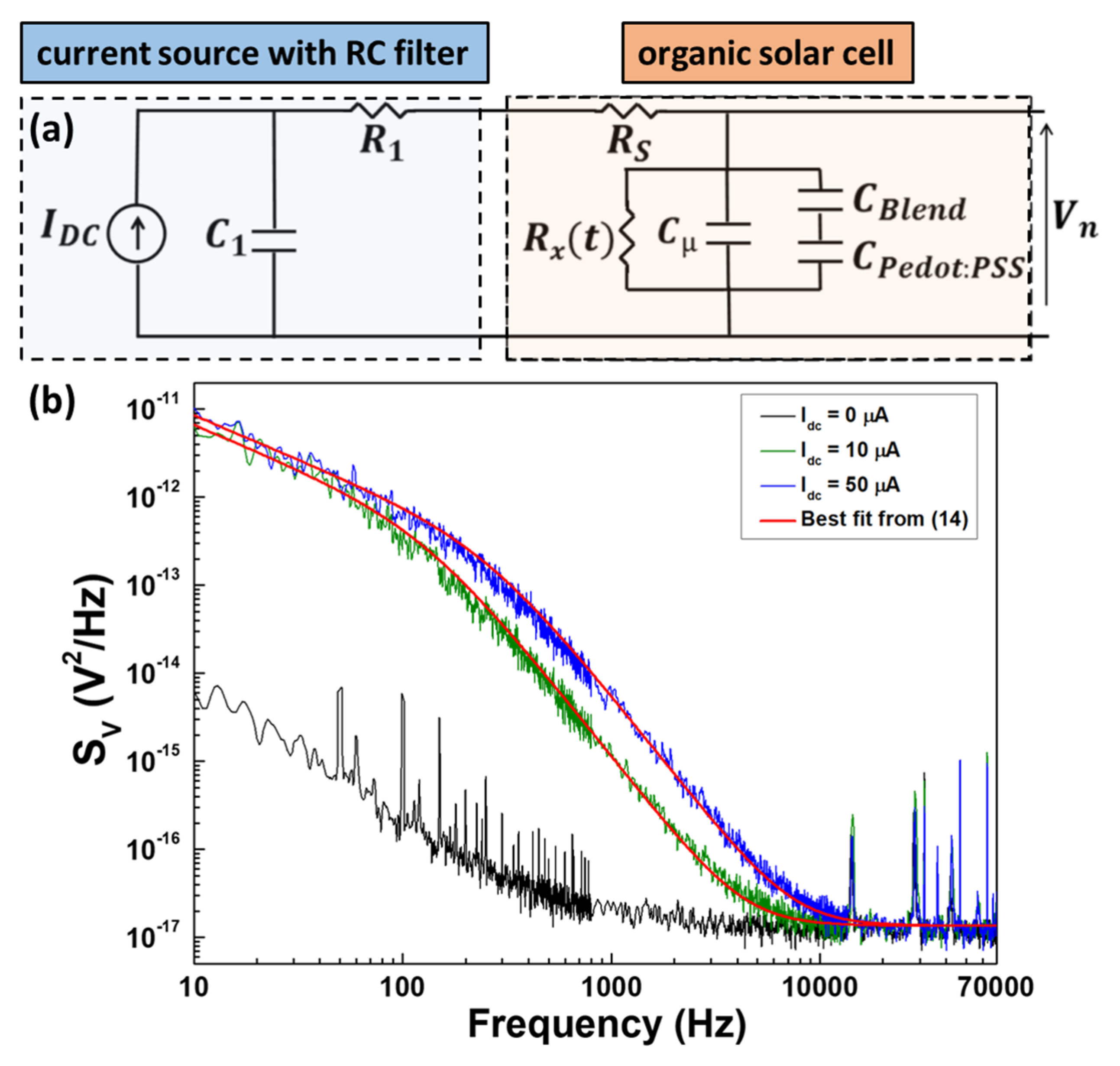
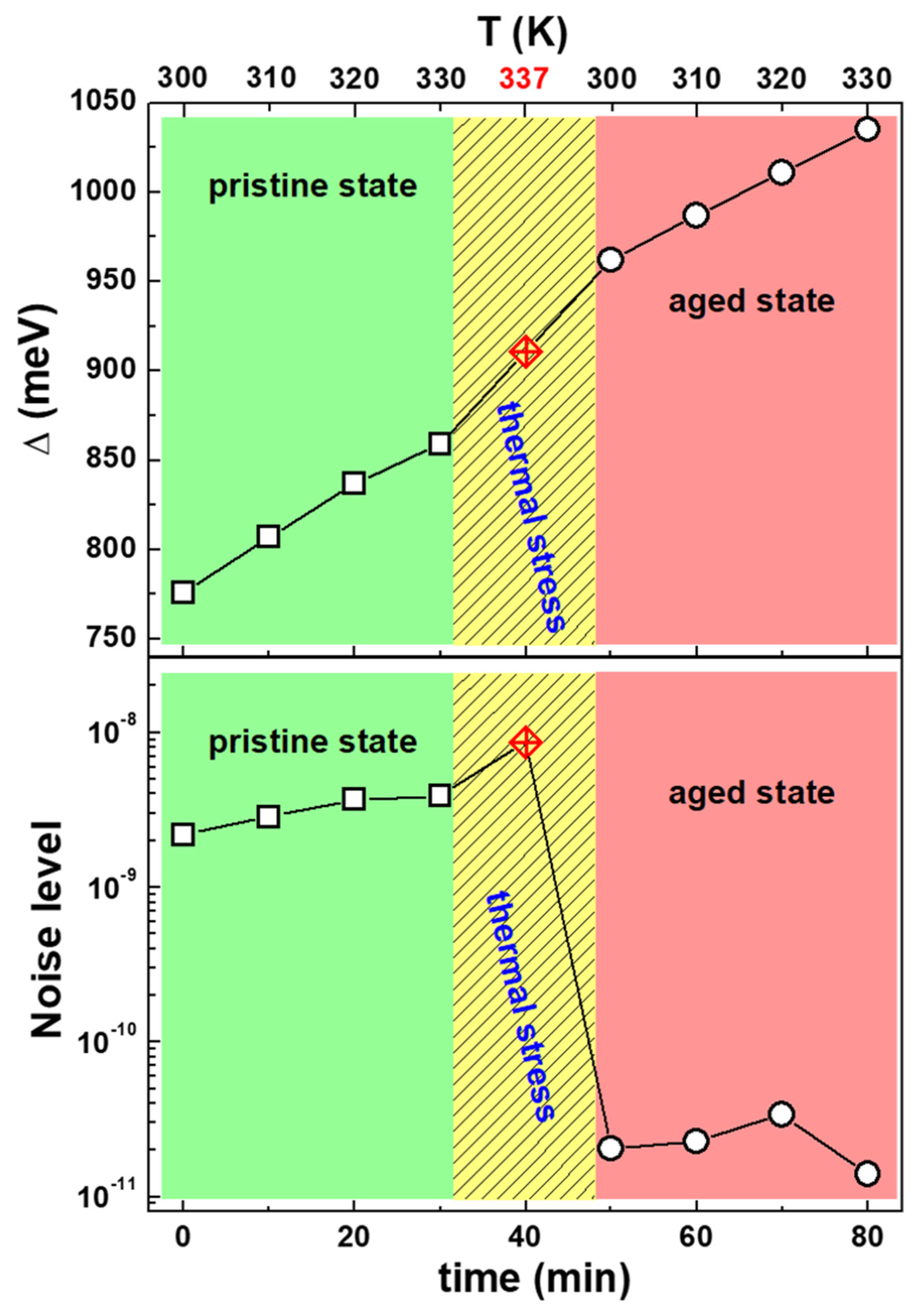
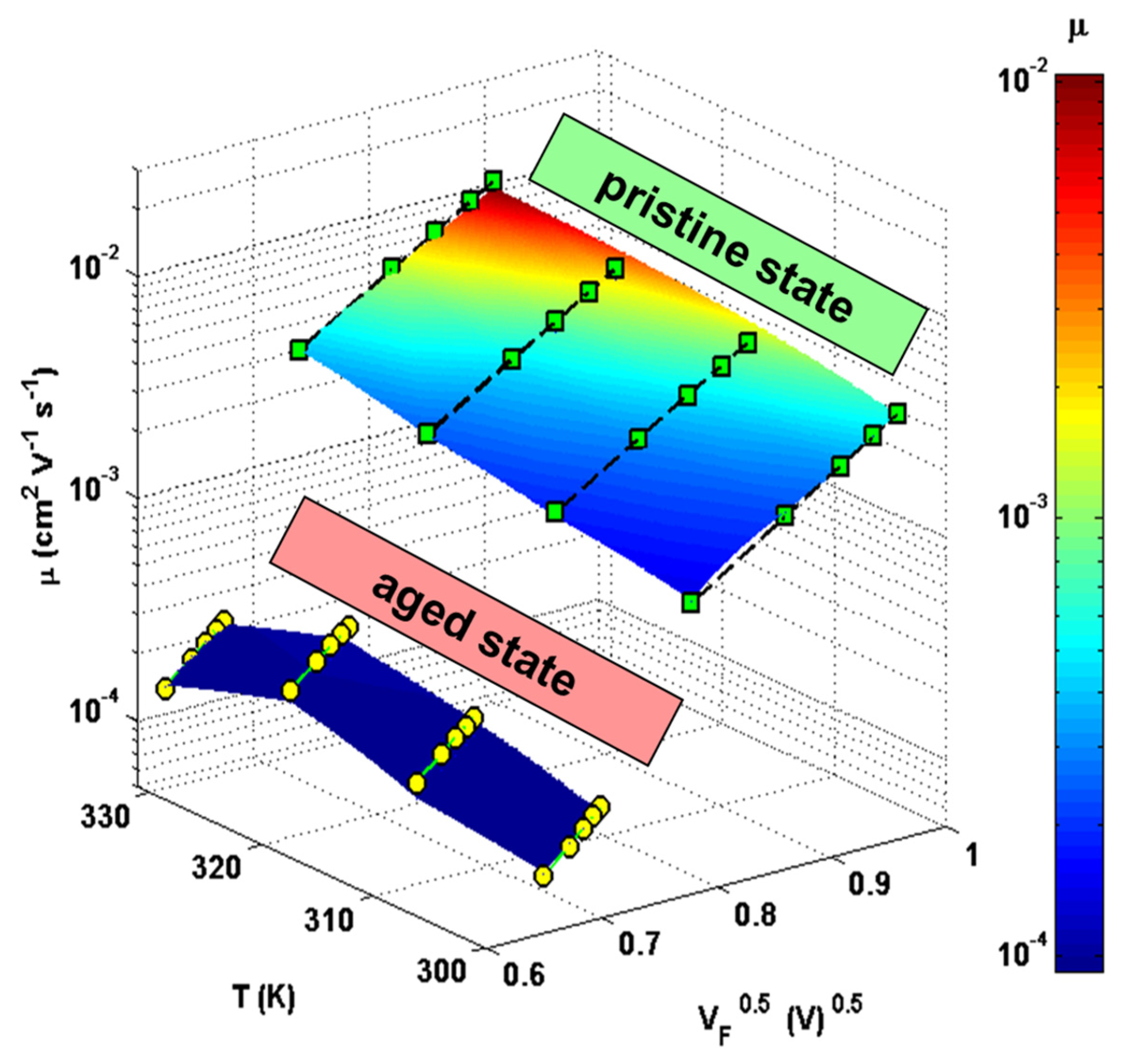
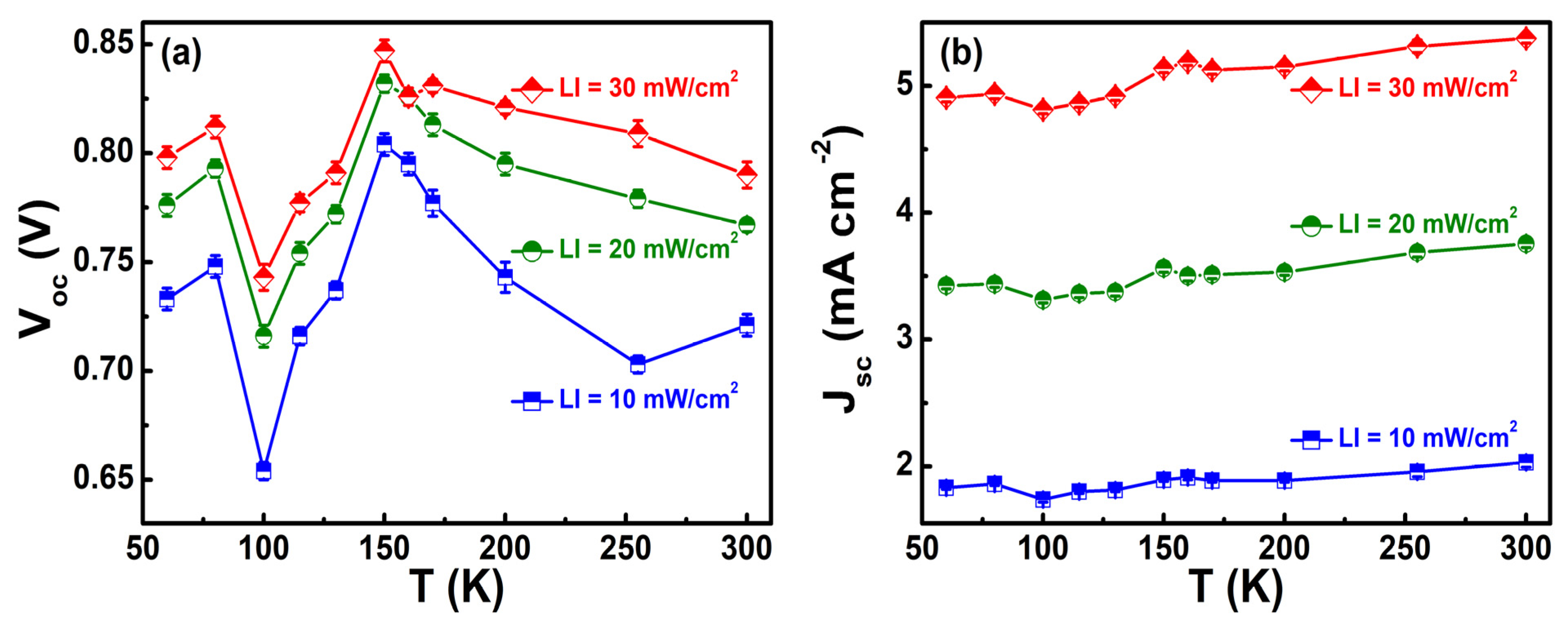
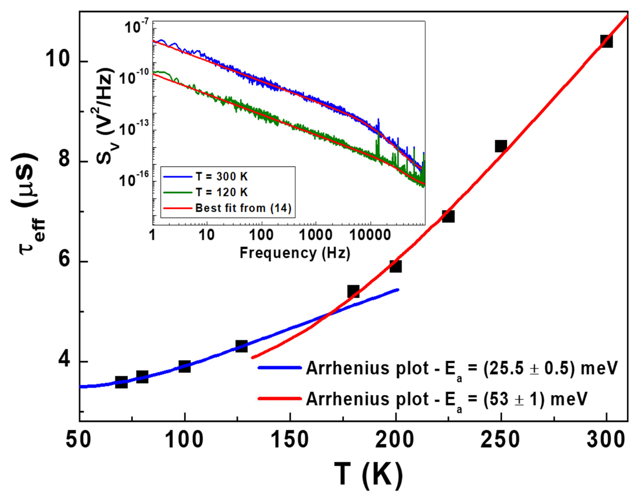
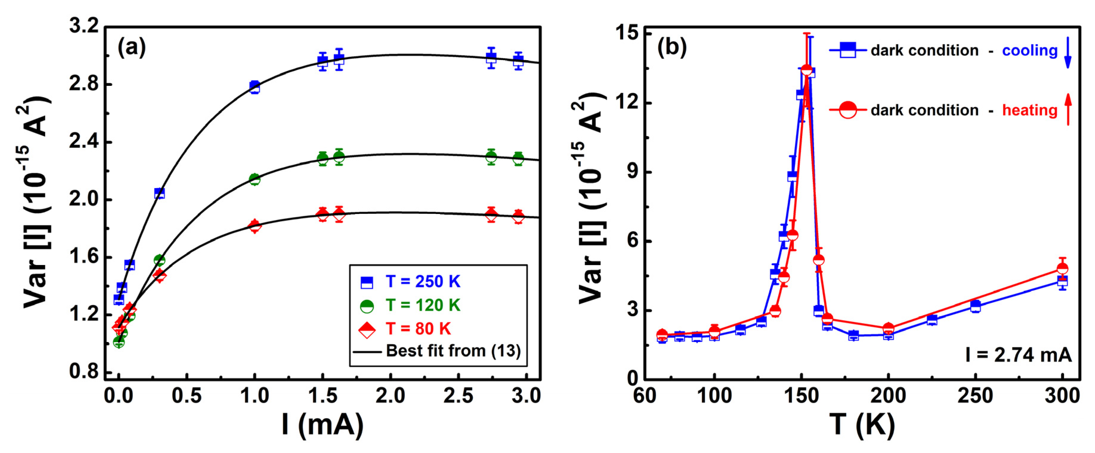
4.2. Physical Modeling and Real-Time Monitoring of Organic Solar Cells through Electric Noise

As fluctuation spectroscopy is a well-known tool for the non-destructive analysis of the transport processes in several systems, it can be used profitably to evaluate the solar cells’ performances, especially in the case of innovative devices based on organic materials. These types of compounds are very sensitive to external perturbations, such as temperature variation and fabrication technology. In particular, the samples investigated herein have an active layer formed by a bulk heterojunction between P3HT and PCBM, dissolved in a mixture of ortho-dichlorobenzene and 1,2,3,4-tetrahydronaphtalene. All the preparation details are reported elsewhere [60]. From the electrical point of view, such a design of the active layer can be regarded as an RC sub-circuit at low frequencies, as evidenced by several studies of the polymer solar cell admittance [171,172]. The same circuit, from the noise point of view, can be modeled as a parallel connection between a fluctuating resistance R x t and a capacitance C x . In Figure 14a, this scheme is shown. The resistance R x is the sum of a small fluctuating random function and of the recombination resistance R r e c of electrons and holes [173], defined in terms of the forward voltage V F and of the DC bias current R r e c = d V F / d I d c without the contribution of the device series resistance R S [174]. The capacitance C x is the sum of the chemical capacitance C μ and the series of two capacitances C B l e n d and C P e d o t : P S S , related to the dielectric contribution of the active layer and the hole transport layer [99]. Since the noise measurements are performed with an active bias of the samples, the equivalent circuital representation in Figure 14a has to take into account the presence of an input DC current source, followed by an RC low pass filter to reduce externally generated noise.
The physical model described here gives an expression for the voltage–spectral density as [99]:
S V f = K f γ R r e c 2 · I d c 2 1 + f / f x 2
where γ is the frequency exponent close to 1 and f x = 2 π C x R r e c 1 is a cutoff frequency. Equation (14) indicates that the main contribution to the measured voltage-noise V n is generated from the parallel R x C x connection, resulting in a dominant 1/ f dependence below f x and in a 1/ f 3 dependence at higher frequencies. The best fitting curves obtained by using Equation (14) are shown in Figure 14b as solid red lines, confirming a good agreement with the experimental data acquired at different values of DC bias (10 μA and 50 μA, green and blue traces, respectively). As evident, the system background noise at 0 μA (black trace in Figure 14b) is negligible, being more than two orders of magnitude lower.
The fitting procedure with Equation (14) allows an estimation of C μ from f x and knowing the series of C B l e n d and C P e d o t : P S S (9.2 nF⋅cm−2, in the case considered here), which is usually obtained from the device size [175]. Given C μ , it is possible to extract the electron density of states (DOS) at a fixed position of the Fermi level as: g E = C μ t 1 e 2 ( t being the active layer thickness and e the electron charge) [176,177]. Moreover, by computing R r e c from the current–voltage characteristics, the electron lifetime can be calculated as: τ n = R r e c C μ [99,171]. All these parameters are reported in Table 1 for a typical investigated organic photovoltaic device, at room temperature and for different energy values E (i.e., E = e · V F ). The data indicate: (I) an opposite behavior of C μ and R r e c as a function of E , essentially due to the storage of minority carriers in the active layer of the solar cell by increasing the forward voltage; (II) an electron lifetime ranging between 0.6 and 0.85 ms, in agreement with the results obtained by using alternative techniques, such as impedance spectroscopy and photo-induced absorption [86,178]; and (III) a DOS that follows a Gaussian distribution, from which it is possible to evaluate the disorder parameter σ n directly related to the solar cell performance [99,176].
It is clear that electric noise spectroscopy gives an informative picture of the device quality, but these measurements are also sensitive to structural changes of the material. To this end, voltage–noise analysis was performed after thermal stress, artificially induced on the organic cells by increasing the operating temperature up to 340 K. Indeed, it is well-known that heating is one of the most important external effects that can accelerate the degradation rate of the organic photoactive compound [21,179]. In particular, in the case of the P3HT:PCBM heterojunction, the temperature increase may induce phase separation between the two layers, leading to a vertical structure detrimental for cell efficiency [180,181]. An indication of the formation of such an undesirable structure can be obtained by studying the current-voltage characteristics of the organic solar cells in terms of the classical Schottky–Richardson emission law [37]. From this theoretical model, it is possible to reproduce the temperature dependence of the barrier energy at the metal-blend interface, whose behavior is shown in Figure 15 (upper panel) for a typical investigated device. During the first thermal cycle up to 337 K, the parameter for the pristine sample is characterized by a clear enhancement, which becomes more evident after cooling to room temperature and the subsequent second thermal cycle (indicated in Figure 15 as the aged state). An explanation of this effect on can be attributed to the thermal stress, which may induce a non-reversible modification of the blend morphology [182] and, consequently, a band discontinuity [13].
While the nature of the active layer modification due to temperature can be revealed through DC analysis, the consequences on the intrinsic properties of the solar cell, such as the charge carrier mobility, have to be determined by the sensitive noise experiments. In more detail, from Equation (14), that is the flicker noise component, it is possible to evaluate the noise level K by fitting the measured voltage–noise traces. The temperature dependence of such a noise level is shown in Figure 15 (lower panel) as a function of the time elapsed between the subsequent measurements. The existence of a noise peak, typical of structural changes [137,183,184], is evident at 337 K, giving a strong indication in favour of the occurrence of a non-reversible process, which takes place between the first and second thermal cycle. Moreover, an abrupt decrease of K , more than two orders of magnitude, is found when the device goes from the pristine to the aged state. The questions are whether the photovoltaic performances and how the electric transport properties are negatively influenced by the thermal stress.
In order to answer the questions raised, a direct evaluation of the electron mobility μ can be made through voltage–noise investigations. In particular, from [185] and [93] it follows:
μ = S V f l i c k e r S V t h e r m a l × k B T e τ n F 2
where S V f l i c k e r derives directly from Equation (14), S V t h e r m a l = 4 k B T R r e c is the well-known Johnson noise contribution, and F = V F / t is the applied electric field (being t the active layer thickness). The mobility values obtained from Equation (15) are shown in Figure 16 as a function of temperature and of the forward voltage, in the pristine and aged states, respectively. A marked reduction of μ is clearly seen, as driven by the thermal stress. The results of Figure 16 are the direct consequence of the noise level reduction observed in Figure 15 and evidence of the fact that degradation phenomena are occurring in the solar cell. As widely reported in the literature, a low charge carrier mobility detrimentally affects the power conversion efficiency [168,186].
Noting the logarithmic ordinate axis in Figure 16, an exponential μ -dependence on V F 1 / 2 (equivalently, on F 1 / 2 ) can be observed, which allows an interpretation in terms of the Poole–Frenkel effect [37,93]. By using this model, the zero-field mobility μ 0 and the Gill energy E G i l l can be extracted. The experimental data reported in Table 2 for a typical investigated P3HT:PCBM device show an increase of μ 0 with temperature during every single thermal cycle, usually attributed to thermally-activated processes. In parallel, a strong reduction is found for aged samples. Moreover, the increase of E G i l l between the first and the second thermal cycle (see Table 2 for details) gives a further confirmation on the occurrence of a non-reversible change in the active layer, as well as in the interface, under the action of rapid temperature variation.
Recent studies have revealed the possibility to realize more stable and performant polymer:fullerene solar cells by preparing blends with the addition of a high boiling point solvent [187,188]. In particular, it has been described that the substitution of the reference solvent 1,2-dichlorobenzene (oDCB) with one of the same type along with the addition of 1,2,3,4-tetrahydronaphthalene (THN) produces photovoltaic devices with a more efficient charge carrier transport in the active layer [60].
Blends prepared with oDCB+THN as a solvent have enhanced values of electron density per unit volume and electron lifetimes [100]. This is essentially due to THN having a higher boiling point (207 °C) than oDCB (180 °C), allowing a net separation between P3HT and PCBM. The consequence is an enhanced ordering of P3HT, which severely limits the charge carrier recombination mechanisms at the donor–acceptor interface. Reducing the processes of recombination and enhancing charge collection means a better morphology of the blend and, consequently, an improvement of the bulk heterojunction solar cell efficiency and a reduction of the degradation rate. Overall, the use of fluctuation spectroscopy has given very important information on the optimization of the blend structure, which is a fundamental requirement to produce high-quality organic solar cells. In this direction, several authors have published further experimental evidence confirming the potential of noise spectroscopy for the fabrication of reliable and high-performing OPVs [189,190].

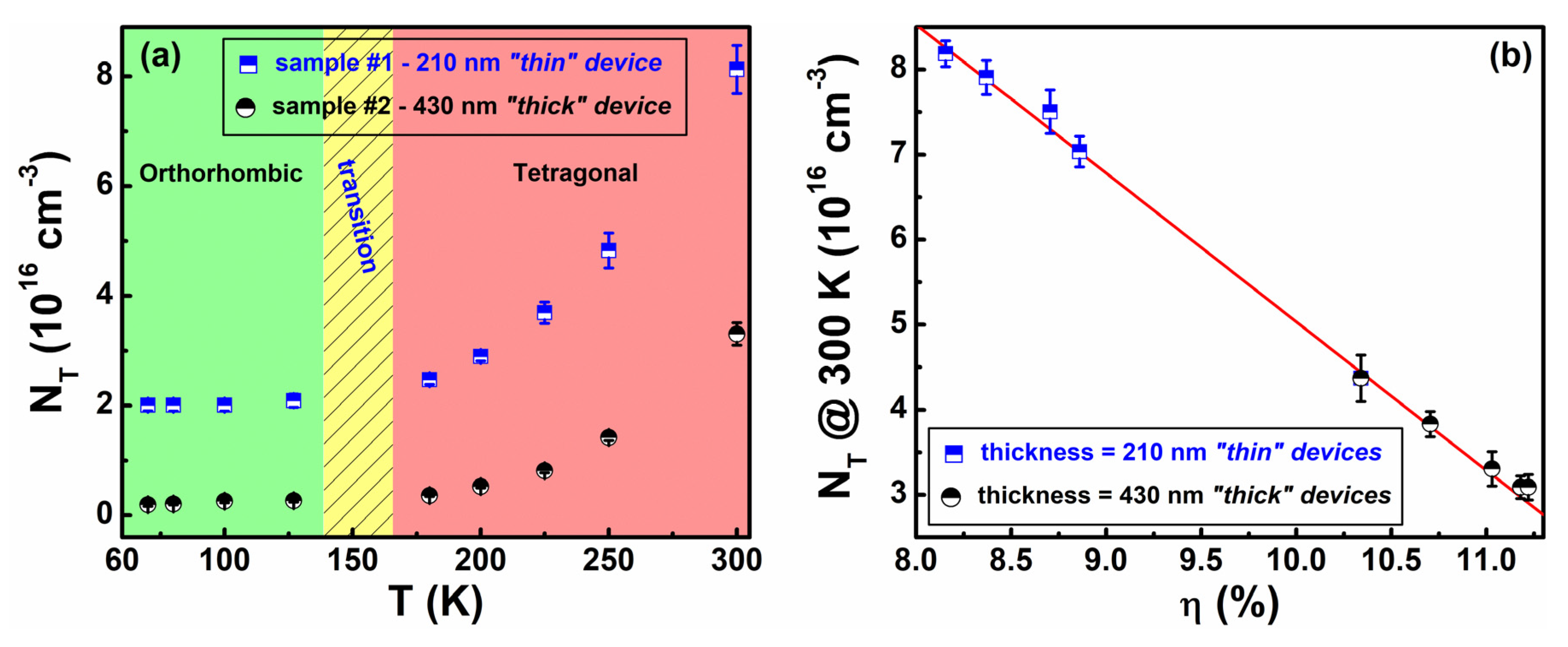
4.3. Material and Efficiency Characterizations of Perovskite Solar Cells by Noise Spectroscopy

The introduction of organic-inorganic hybrid perovskite materials in the fabrication of dye-sensitized solar cells has revealed its potential to improve the power conversion efficiency [27]. Moreover, elevated charge carrier mobilities [27], diffusion lengths of the order of micrometers [191], and long charge carrier lifetimes [192] are very peculiar characteristics of perovskites that can be used for the development of a new and competitive photovoltaic technology, functional for terrestrial and space applications [28]. In recent years, perovskite-based solar cells have also been employed for low-power indoor applications [193]. However, from the applicability point of view, the physical properties that make hybrid perovskites so promising for solar energy conversion are not completely understood [194]. In particular, how defect states’ distribution impacts the carrier recombination and device performance is still an open issue [195,196]. In this respect, the experimental results obtained with standard characterizations, such as low-frequency dielectric and nuclear magnetic resonance measurements, give additional information on the carrier kinetic processes in action, but are less sensitive in revealing changes in the structural properties of the system investigated. This last aspect is very crucial in the case of solar cell devices based on perovskite materials, which are characterized, for example, by a low-temperature transition from a tetragonal to an orthorhombic structure [197], not visible from the DC analysis.
Triggered by these motivations, noise spectroscopy experiments have been performed on perovskite solar cells composed of a methylammonium lead iodide CH3NH3PbI3 absorber layer sandwiched between the electron and hole transport layers. All the details of the device preparation are reported elsewhere [28,32,102]. The resulting stable and highly reproducible solar cells had a rather high efficiency around 18% [198]. It is well-known, however, that the photovoltaic properties are modified when the temperature is lowered. In particular, the open-circuit voltage V o c (Figure 17a) exhibits a maximum in the 140–160 K temperature range and a minimum value close to 100 K. A less evident peak near 160 K is also observed in the temperature dependence of the short-circuit current density J s c (Figure 17b), and a similar minimum as V o c is found at 100 K. This behavior, independent of the light intensity, suggests the occurrence of a modification in the electrical conduction of the perovskite devices, but no specific information can be extracted on the nature of this phenomenon by DC measurements alone. In order to shed light on this aspect, electric noise can be very useful.
As already seen for reference Si-based and polymer:fullerene solar cells, the origin of the charge carrier fluctuations can be explained in terms of a theoretical model that combines trapping/detrapping and recombination mechanisms. In this framework, the frequency dependence of the voltage-noise spectrum can be described with Equation (14), which shows the presence of a 1/ f component at low frequencies followed by a change from a 1/ f to a 1/ f 3 behavior at a cutoff frequency f x . Recently, Sangwan et al. have reported a similar trend, evidencing a knee in the noise spectra for the perovskite-based solar cells [105]. A good agreement between the noise data and the fitting formula of Equation (14) is clearly visible in the inset of Figure 18, where S V measured at a fixed bias current of 0.02 mA and different temperatures are shown. From the best-fitting curves (solid red lines in the inset of Figure 18), it is possible to extract the parameter f x and, consequently, the effective lifetime coefficient τ e f f = 2 π f x 1 . The temperature dependence of τ e f f , analyzed with the Arrhenius equation, allows us to identify two distinct activation energies E a of the fluctuating traps. In particular, a E a = 25.5 ± 0.5 meV in the low-temperature region (blue curve in Figure 18) and a E a = 53 ± 1 meV at high temperatures (red curve in Figure 18) have been found. Similar behavior of τ e f f with similar values of E a has been already reported for CH3NH3PbI3 solar cells by using measurements from photovoltage decay [81], and from impedance spectroscopy, which also evidences a change of the τ e f f slope around [140–160] K [199]. What happens in this temperature range?
In order to give a response to the question above, the properties of fluctuation mechanisms have been correlated with the characteristic solar cell parameters of the dominant defect centers. Therefore, the current–noise variance V a r I has been computed and its dependence as a function of the total current I (either DC-biased or photogenerated) is shown in Figure 19a at different temperatures. By fixing I , the presence of a noise peak between 140 and 160 K is clearly observed (see Figure 19b for details). This feature seems to be intrinsically related to the perovskite material and it is not a measurement artifact, being verified by measuring the samples in cooling (blue squares in Figure 19b) and in heating (red circles in Figure 19b) modes.
Here, it is evident that no hysteretic effects are present in the experimental results. The unexpected additional noise level near 160 K is essentially due to a random distribution of microscopic phases, which are formed by a structural reorganization of the perovskite compound. The resistance associated with these microscopic phases randomly fluctuates, generating an excess 1/ f noise in the transition region. The latter represents the crossover between tetragonal and orthorhombic phases of the material that, from the noise point of view, can be identified by the change from a trapping/detrapping to a resistance fluctuation mechanism [32,102,167].
It is clear, however, that outside the transition region, the noise modeling is similar to what is already described for Si-based and organic solar cells. In particular, Equation (13) establishes a combination of trapping/detrapping related processes and charge carrier recombination phenomena [101]. From this interpretation, it follows that the best fitting curves, shown in Figure 19a as solid black lines, are obtained by using Equation (13), whose parameters estimation allows us to compute the fluctuating trap density N T . From the temperature dependence of N T in Figure 20a, it is noted that below 140 K, N T remains almost constant at 2 × 10 16 cm−3 for thinner devices (blue squares in Figure 20a) and at 2 × 10 15 cm−3 for thicker devices (black circles in Figure 20a). Above 160 K, instead, a net increase of N T is observed and can be related to the presence of thermally-activated atomic vacancies, a common type of point defects in perovskite structures [200,201]. The temperature region between 140 and 160 K can be clearly identified as a transition region, where the perovskite structural phase transformation takes place, confirming the results obtained with the current–noise variance.
A direct correlation between the density of the defect states and the power conversion efficiency can be made by analyzing the experimental data acquired on perovskite solar cells of different active layer thicknesses, characterized by distinct efficiency values ranging from 8% to 11.5% at 300 K. Figure 20b shows a general decreasing dependence of N T by increasing η , indicating that, as expected, the improvement of the photovoltaic performance is realized when the number of defects is reduced. It is worth mentioning that the thick devices, characterized by a lower defect density and then higher performance, exhibit a lower noise amplitude contribution. This experimental result, confirmed by several works reported in the literature [120,202,203,204], certifies that electric noise spectroscopy gives information not only on the physical mechanisms and properties of the system under test, but it is also fundamental for the photovoltaic device reliability and quality evaluation.

5. Conclusions

In summary, a non-destructive electrical characterization technique based on low-frequency noise spectroscopy has been implemented to describe transport processes, recombination mechanisms, and morphological/structural changes in different photovoltaic technologies. In Figure 21, a flowchart describing the methodology for extracting the parameters from the noise spectra analysis is reported.
As evidenced, parameters describing the charge transport, recombination kinetics, and structural and morphological changes are extracted from the noise amplitude and the shape of the noise spectra and are correlated to the device performance through appropriate AC modeling. For the organic solar cell, the noise analysis is very sensitive to the morphological and structural modifications occurring in the devices during degradation. The charge carrier lifetime and mobility have been extracted directly from the noise spectra. In pristine and proton-degraded silicon solar cells, the difference between dark and photo-induced noise has been evaluated by using a noise model that combines the trapping/detrapping and the recombination mechanisms. For the perovskite-based devices, the dynamics of the fluctuations detect the existence of a metastable state in a crossover region between the room-temperature tetragonal and the low-temperature orthorhombic phases of the perovskite compound. The use of noise spectroscopy reveals that, in perovskite solar cells, the recombination kinetics is strongly influenced by the electron–phonon interactions. A clear correlation between the morphological structure of the perovskite grains, the energy disorder of the defect states, and the device performance is demonstrated.
Overall, it is evident that the noise experimental technique can provide, through a specific physical modeling as shown in Figure 21, significant parameter extraction useful for the assessment of the device performances and reliability. Therefore, it should be considered as one of the main tools to understand physical properties of photovoltaic technologies.

Author Contributions

All authors have contributed to the conceptualization, writing, review, and editing of the manuscript. The published version of the manuscript has been read and approved by all authors. All authors have read and agreed to the published version of the manuscript.

Funding

C.B. and S.P. acknowledge partial support from the University of Salerno through grants 300391FRB19PAGAN, 300391FRB20BARON, 300391FRB21CAVAL, and 300391FRB22PAGAN. INFN is also gratefully acknowledged through experiments Qub-IT and DARTWARS.

Data Availability Statement

The data presented in this study are not publicly available. Data are, however, available from the authors upon reasonable request and with permission of the University of Salerno.

Acknowledgments

Salvatore Abate from CNR-SPIN Salerno (Italy) is gratefully acknowledged for his technical support. Antonietta De Sio from Oldenburg University (Germany) is gratefully acknowledged for the preparation and preliminary characterization of the organic solar cells. Felix Lang, Steve Albrecht, Jörg Rappich, Norbert H. Nickel, and Bernd Rech from Helmholtz-Zentrum Berlin (Germany) are gratefully acknowledged for the preparation and efficient characterization of the perovskite-based photovoltaic devices.

Conflicts of Interest

The authors declare no conflict of interest.

References

  1. IEA. Electricity Market Report—January 2022; IEA: Paris, France, 2022. [Google Scholar]
  2. Kabeyi, M.J.B.; Olanrewaju, O.A. Sustainable Energy Transition for Renewable and Low Carbon Grid Electricity Generation and Supply. Front. Energy Res. 2022, 9, 743114. [Google Scholar] [CrossRef]
  3. Becquerel, A.E. Memoire Sur Les Effects d’Electriques Produits Sous l’Influence Des Rayons Solaires. Comptes Rendus L’academie Sci. 1839, 9, 561–567. [Google Scholar]
  4. IEA. Special Report on Solar PV Global Supply Chains; IEA: Paris, France, 2022. [Google Scholar]
  5. Vijaya, S.; Landi, G.; Wu, J.J.; Anandan, S. Ni3S4/CoS2 Mixed-Phase Nanocomposite as Counter Electrode for Pt-Free Dye-Sensitized Solar Cells. J. Power Sources 2020, 478, 229068. [Google Scholar] [CrossRef]
  6. Subbiah, V.; Landi, G.; Wu, J.J.; Anandan, S. MoS2 Coated CoS2 Nanocomposites as Counter Electrodes in Pt-Free Dye-Sensitized Solar Cells. Phys. Chem. Chem. Phys. 2019, 21, 25474–25483. [Google Scholar] [CrossRef] [PubMed]
  7. Kim, J.-H.; Kim, D.-H.; So, J.-H.; Koo, H.-J. Toward Eco-Friendly Dye-Sensitized Solar Cells (DSSCs): Natural Dyes and Aqueous Electrolytes. Energies 2021, 15, 219. [Google Scholar] [CrossRef]
  8. Yan, J.; Saunders, B.R. Third-Generation Solar Cells: A Review and Comparison of Polymer:Fullerene, Hybrid Polymer and Perovskite Solar Cells. RSC Adv. 2014, 4, 43286–43314. [Google Scholar] [CrossRef] [Green Version]
  9. Ding, G.; Zheng, Y.; Xiao, X.; Cheng, H.; Zhang, G.; Shi, Y.; Shao, Y. Sustainable Development of Perovskite Solar Cells: Keeping a Balance between Toxicity and Efficiency. J. Mater. Chem. A 2022, 10, 8159–8171. [Google Scholar] [CrossRef]
  10. Zhang, J.; Chang, N.; Fagerholm, C.; Qiu, M.; Shuai, L.; Egan, R.; Yuan, C. Techno-Economic and Environmental Sustainability of Industrial-Scale Productions of Perovskite Solar Cells. Renew. Sustain. Energy Rev. 2022, 158, 112146. [Google Scholar] [CrossRef]
  11. Mahapatra, A.; Prochowicz, D.; Tavakoli, M.M.; Trivedi, S.; Kumar, P.; Yadav, P. A Review of Aspects of Additive Engineering in Perovskite Solar Cells. J. Mater. Chem. A 2020, 8, 27–54. [Google Scholar] [CrossRef]
  12. Trivedi, S.; Prochowicz, D.; Parikh, N.; Mahapatra, A.; Pandey, M.K.; Kalam, A.; Tavakoli, M.M.; Yadav, P. Recent Progress in Growth of Single-Crystal Perovskites for Photovoltaic Applications. ACS Omega 2021, 6, 1030–1042. [Google Scholar] [CrossRef] [PubMed]
  13. Barone, C.; Landi, G.; De Sio, A.; Neitzert, H.C.; Pagano, S. Thermal Ageing of Bulk Heterojunction Polymer Solar Cells Investigated by Electric Noise Analysis. Sol. Energy Mater. Sol. Cells 2014, 122, 40–45. [Google Scholar] [CrossRef]
  14. Zhao, J.; Li, Y.; Yang, G.; Jiang, K.; Lin, H.; Ade, H.; Ma, W.; Yan, H. Efficient Organic Solar Cells Processed from Hydrocarbon Solvents. Nat. Energy 2016, 1, 15027. [Google Scholar] [CrossRef]
  15. Brabec, C.J.; Gowrisanker, S.; Halls, J.J.M.; Laird, D.; Jia, S.; Williams, S.P. Polymer-Fullerene Bulk-Heterojunction Solar Cells. Adv. Mater. 2010, 22, 3839–3856. [Google Scholar] [CrossRef] [PubMed]
  16. Ma, W.; Yang, C.; Gong, X.; Lee, K.; Heeger, A.J. Thermally Stable, Efficient Polymer Solar Cells with Nanoscale Control of the Interpenetrating Network Morphology. Adv. Funct. Mater. 2005, 15, 1617–1622. [Google Scholar] [CrossRef]
  17. Hashemi, S.A.; Ramakrishna, S.; Aberle, A.G. Recent Progress in Flexible-Wearable Solar Cells for Self-Powered Electronic Devices. Energy Environ. Sci. 2020, 13, 685–743. [Google Scholar] [CrossRef]
  18. Lee, S.H.; Kim, J.H.; Shim, T.H.; Park, J.G. Effect of Interface Thickness on Power Conversion Efficiency of Polymer Photovoltaic Cells. Electron. Mater. Lett. 2009, 5, 47–50. [Google Scholar] [CrossRef]
  19. Green, M.A.; Dunlop, E.D.; Hohl-Ebinger, J.; Yoshita, M.; Kopidakis, N.; Bothe, K.; Hinken, D.; Rauer, M.; Hao, X. Solar Cell Efficiency Tables (Version 60). Prog. Photovolt. Res. Appl. 2022, 30, 687–701. [Google Scholar] [CrossRef]
  20. Green, M.; Dunlop, E.; Hohl-Ebinger, J.; Yoshita, M.; Kopidakis, N.; Hao, X. Solar Cell Efficiency Tables (Version 57). Prog. Photovoltaics Res. Appl. 2021, 29, 3–15. [Google Scholar] [CrossRef]
  21. Tromholt, T.; Manceau, M.; Helgesen, M.; Carlé, J.E.; Krebs, F.C. Degradation of Semiconducting Polymers by Concentrated Sunlight. Sol. Energy Mater. Sol. Cells 2011, 95, 1308–1314. [Google Scholar] [CrossRef]
  22. Yang, S.-S.; Hsieh, Z.-C.; Keshtov, M.L.; Sharma, G.D.; Chen, F.-C. Toward High-Performance Polymer Photovoltaic Devices for Low-Power Indoor Applications. Sol. RRL 2017, 1, 1700174. [Google Scholar] [CrossRef]
  23. Landi, G.; Granata, V.; Germano, R.; Pagano, S.; Barone, C. Low-Power and Eco-Friendly Temperature Sensor Based on Gelatin Nanocomposite. Nanomaterials 2022, 12, 2227. [Google Scholar] [CrossRef] [PubMed]
  24. Landi, G.; Neitzert, H.-C. Application of a Bio-Nanocomposite Tissue as an NIR Optical Receiver and a Temperature Sensor. ACS Appl. Electron. Mater. 2021, 3, 2790–2797. [Google Scholar] [CrossRef]
  25. La Notte, L.; Giordano, L.; Calabrò, E.; Bedini, R.; Colla, G.; Puglisi, G.; Reale, A. Hybrid and Organic Photovoltaics for Greenhouse Applications. Appl. Energy 2020, 278, 115582. [Google Scholar] [CrossRef]
  26. Fan, R.; Huang, Y.; Wang, L.; Li, L.; Zheng, G.; Zhou, H. The Progress of Interface Design in Perovskite-Based Solar Cells. Adv. Energy Mater. 2016, 6, 1600460. [Google Scholar] [CrossRef]
  27. Green, M.A.; Ho-Baillie, A.; Snaith, H.J. The Emergence of Perovskite Solar Cells. Nat. Photonics 2014, 8, 506–514. [Google Scholar] [CrossRef]
  28. Lang, F.; Nickel, N.H.; Bundesmann, J.; Seidel, S.; Denker, A.; Albrecht, S.; Brus, V.V.; Rappich, J.; Rech, B.; Landi, G.; et al. Radiation Hardness and Self-Healing of Perovskite Solar Cells. Adv. Mater. 2016, 28, 8726–8731. [Google Scholar] [CrossRef] [PubMed] [Green Version]
  29. Song, Z.; McElvany, C.L.; Phillips, A.B.; Celik, I.; Krantz, P.W.; Watthage, S.C.; Liyanage, G.K.; Apul, D.; Heben, M.J. A Technoeconomic Analysis of Perovskite Solar Module Manufacturing with Low-Cost Materials and Techniques. Energy Environ. Sci. 2017, 10, 1297–1305. [Google Scholar] [CrossRef]
  30. Siegler, T.D.; Dawson, A.; Lobaccaro, P.; Ung, D.; Beck, M.E.; Nilsen, G.; Tinker, L.L. The Path to Perovskite Commercialization: A Perspective from the United States Solar Energy Technologies Office. ACS Energy Lett. 2022, 7, 1728–1734. [Google Scholar] [CrossRef]
  31. Palma, A.L. Laser-Processed Perovskite Solar Cells and Modules. Sol. RRL 2020, 4, 1900432. [Google Scholar] [CrossRef]
  32. Landi, G.; Neitzert, H.C.; Barone, C.; Mauro, C.; Lang, F.; Albrecht, S.; Rech, B.; Pagano, S. Correlation between Electronic Defect States Distribution and Device Performance of Perovskite Solar Cells. Adv. Sci. 2017, 4, 1700183. [Google Scholar] [CrossRef]
  33. An, Q.; Paulus, F.; Becker-Koch, D.; Cho, C.; Sun, Q.; Weu, A.; Bitton, S.; Tessler, N.; Vaynzof, Y. Small Grains as Recombination Hot Spots in Perovskite Solar Cells. Matter 2021, 4, 1683–1701. [Google Scholar] [CrossRef]
  34. Ren, A.; Lai, H.; Hao, X.; Tang, Z.; Xu, H.; Yu Jeco, B.M.F.; Watanabe, K.; Wu, L.; Zhang, J.; Sugiyama, M.; et al. Efficient Perovskite Solar Modules with Minimized Nonradiative Recombination and Local Carrier Transport Losses. Joule 2020, 4, 1263–1277. [Google Scholar] [CrossRef]
  35. Zhang, D.; Li, D.; Hu, Y.; Mei, A.; Han, H. Degradation Pathways in Perovskite Solar Cells and How to Meet International Standards. Commun. Mater. 2022, 3, 58. [Google Scholar] [CrossRef]
  36. Long, B.; Zhou, X.; Cao, H.; Chen, R.; He, N.; Chi, L.; Fan, P.; Chen, X. Excellent Stability of Perovskite Solar Cells Encapsulated With Paraffin/Ethylene-Vinyl Acetate/Paraffin Composite Layer. Front. Mater. 2022, 9, 892657. [Google Scholar] [CrossRef]
  37. Sze, S.M.; Kwok, K. Ng Physics of Semiconductor Devices, 3rd ed.; John Wiley & Sons: Hoboken, NJ, USA, 2006. [Google Scholar]
  38. Battaglia, C.; Cuevas, A.; De Wolf, S. High-Efficiency Crystalline Silicon Solar Cells: Status and Perspectives. Energy Environ. Sci. 2016, 9, 1552–1576. [Google Scholar] [CrossRef] [Green Version]
  39. De Wolf, S.; Holovsky, J.; Moon, S.J.; Löper, P.; Niesen, B.; Ledinsky, M.; Haug, F.J.; Yum, J.H.; Ballif, C. Organometallic Halide Perovskites: Sharp Optical Absorption Edge and Its Relation to Photovoltaic Performance. J. Phys. Chem. Lett. 2014, 5, 1035–1039. [Google Scholar] [CrossRef]
  40. Bhattacharya, S.; John, S. Beyond 30% Conversion Efficiency in Silicon Solar Cells: A Numerical Demonstration. Sci. Rep. 2019, 9, 1–15. [Google Scholar] [CrossRef] [PubMed] [Green Version]
  41. ITPRV. International Technology Roadmap for Photovoltaic. In ITRPV 2021, 13th ed.; VDMA: Frankfurt, Germany, 2022; p. 53. [Google Scholar]
  42. Renno, C.; Petito, F.; Landi, G.; Neitzert, H.C. Experimental Characterization of a Concentrating Photovoltaic System Varying the Light Concentration. Energy Convers. Manag. 2017, 138, 119–130. [Google Scholar] [CrossRef]
  43. Li, J.; Aierken, A.; Liu, Y.; Zhuang, Y.; Yang, X.; Mo, J.H.; Fan, R.K.; Chen, Q.Y.; Zhang, S.Y.; Huang, Y.M.; et al. A Brief Review of High Efficiency III-V Solar Cells for Space Application. Front. Phys. 2021, 8, 1–15. [Google Scholar] [CrossRef]
  44. Goetzberger, A.; Knobloch, J.; Voß, B. Crystalline Silicon Solar Cells; John Wiley & Sons, Ltd.: Chichester, UK, 2014; ISBN 9781119033769. [Google Scholar]
  45. Yoshikawa, K.; Kawasaki, H.; Yoshida, W.; Irie, T.; Konishi, K.; Nakano, K.; Uto, T.; Adachi, D.; Kanematsu, M.; Uzu, H.; et al. Silicon Heterojunction Solar Cell with Interdigitated Back Contacts for a Photoconversion Efficiency over 26%. Nat. Energy 2017, 2, 17032. [Google Scholar] [CrossRef]
  46. Liu, Y.; Li, Y.; Wu, Y.; Yang, G.; Mazzarella, L.; Procel-Moya, P.; Tamboli, A.C.; Weber, K.; Boccard, M.; Isabella, O.; et al. High-Efficiency Silicon Heterojunction Solar Cells: Materials, Devices and Applications. Mater. Sci. Eng. R Rep. 2020, 142, 100579. [Google Scholar] [CrossRef]
  47. Haase, F.; Hollemann, C.; Schäfer, S.; Merkle, A.; Rienäcker, M.; Krügener, J.; Brendel, R.; Peibst, R. Laser Contact Openings for Local Poly-Si-Metal Contacts Enabling 26.1%-Efficient POLO-IBC Solar Cells. Sol. Energy Mater. Sol. Cells 2018, 186, 184–193. [Google Scholar] [CrossRef]
  48. Shockley, W.; Queisser, H.J. Detailed Balance Limit of Efficiency of P-n Junction Solar Cells. J. Appl. Phys. 1961, 32, 510–519. [Google Scholar] [CrossRef]
  49. Green, M.A. Third Generation Photovoltaics: Solar Cells for 2020 and Beyond. Phys. E Low-Dimens. Syst. Nanostruct. 2002, 14, 65–70. [Google Scholar] [CrossRef]
  50. Tang, C.W. Two-layer Organic Photovoltaic Cell. Appl. Phys. Lett. 1986, 48, 183–185. [Google Scholar] [CrossRef]
  51. Chamberlain, G.A. Organic Solar Cells: A Review. Sol. Cells 1983, 8, 47–83. [Google Scholar] [CrossRef]
  52. Halls, J.J.M.; Walsh, C.A.; Greenham, N.C.; Marseglia, E.A.; Friend, R.H.; Moratti, S.C.; Holmes, A.B. Efficient Photodiodes from Interpenetrating Polymer Networks. Nature 1995, 376, 498–500. [Google Scholar] [CrossRef]
  53. Yu, G.; Gao, J.; Hummelen, J.C.; Wudl, F.; Heeger, A.J. Polymer Photovoltaic Cells: Enhanced Efficiencies via a Network of Internal Donor-Acceptor Heterojunctions. Science 1995, 270, 1789–1791. [Google Scholar] [CrossRef] [Green Version]
  54. Shaheen, S.E.; Brabec, C.J.; Sariciftci, N.S.; Padinger, F.; Fromherz, T.; Hummelen, J.C. 2.5% Efficient Organic Plastic Solar Cells. Appl. Phys. Lett. 2001, 78, 841–843. [Google Scholar] [CrossRef] [Green Version]
  55. Scharber, M.C.; Sariciftci, N.S. Efficiency of Bulk-Heterojunction Organic Solar Cells. Prog. Polym. Sci. 2013, 38, 1929–1940. [Google Scholar] [CrossRef] [Green Version]
  56. Service, R.F. Outlook Brightens for Plastic Solar Cells. Science 2011, 332, 293. [Google Scholar] [CrossRef]
  57. Würfel, U.; Herterich, J.; List, M.; Faisst, J.; Bhuyian, M.F.M.; Schleiermacher, H.-F.; Knupfer, K.T.; Zimmermann, B. A 1 cm2 Organic Solar Cell with 15.2% Certified Efficiency: Detailed Characterization and Identification of Optimization Potential. Sol. RRL 2021, 5, 2000802. [Google Scholar] [CrossRef]
  58. Gregg, B.A.; Hanna, M.C. Comparing Organic to Inorganic Photovoltaic Cells: Theory, Experiment, and Simulation. J. Appl. Phys. 2003, 93, 3605–3614. [Google Scholar] [CrossRef]
  59. Street, R.A. Carrier Mobility, Structural Order, and Solar Cell Efficiency of Organic Heterojunction Devices. Appl. Phys. Lett. 2008, 93, 133308. [Google Scholar] [CrossRef]
  60. De Sio, A.; Madena, T.; Huber, R.; Parisi, J.; Neyshtadt, S.; Deschler, F.; Da Como, E.; Esposito, S.; von Hauff, E. Solvent Additives for Tuning the Photovoltaic Properties of Polymer–Fullerene Solar Cells. Sol. Energy Mater. Sol. Cells 2011, 95, 3536–3542. [Google Scholar] [CrossRef]
  61. Gao, P.; Grätzel, M.; Nazeeruddin, M.K. Organohalide Lead Perovskites for Photovoltaic Applications. Energy Environ. Sci. 2014, 7, 2448–2463. [Google Scholar] [CrossRef]
  62. Liu, M.; Johnston, M.B.; Snaith, H.J. Efficient Planar Heterojunction Perovskite Solar Cells by Vapour Deposition. Nature 2013, 501, 395–398. [Google Scholar] [CrossRef] [PubMed]
  63. Koh, T.M.; Fu, K.; Fang, Y.; Chen, S.; Sum, T.C.; Mathews, N.; Mhaisalkar, S.G.; Boix, P.P.; Baikie, T. Formamidinium-Containing Metal-Halide: An Alternative Material for near-IR Absorption Perovskite Solar Cells. J. Phys. Chem. C 2014, 118, 16458–16462. [Google Scholar] [CrossRef]
  64. Choi, H.; Jeong, J.; Kim, H.-B.; Kim, S.; Walker, B.; Kim, G.-H.; Kim, J.Y. Cesium-Doped Methylammonium Lead Iodide Perovskite Light Absorber for Hybrid Solar Cells. Nano Energy 2014, 7, 80–85. [Google Scholar] [CrossRef]
  65. Saliba, M.; Matsui, T.; Domanski, K.; Seo, J.-Y.; Ummadisingu, A.; Zakeeruddin, S.M.; Correa-Baena, J.-P.; Tress, W.R.; Abate, A.; Hagfeldt, A.; et al. Incorporation of Rubidium Cations into Perovskite Solar Cells Improves Photovoltaic Performance. Science 2016, 354, 206–209. [Google Scholar] [CrossRef] [PubMed]
  66. Kojima, A.; Teshima, K.; Shirai, Y.; Miyasaka, T. Organometal Halide Perovskites as Visible-Light Sensitizers for Photovoltaic Cells. J. Am. Chem. Soc. 2009, 131, 6050–6051. [Google Scholar] [CrossRef] [PubMed]
  67. Jeong, M.; Choi, I.W.; Go, E.M.; Cho, Y.; Kim, M.; Lee, B.; Jeong, S.; Jo, Y.; Choi, H.W.; Lee, J.; et al. Stable Perovskite Solar Cells with Efficiency Exceeding 24.8% and 0.3-V Voltage Loss. Science 2020, 369, 1615–1620. [Google Scholar] [CrossRef] [PubMed]
  68. Palma, A.L.; Cinà, L.; Busby, Y.; Marsella, A.; Agresti, A.; Pescetelli, S.; Pireaux, J.-J.; Di Carlo, A. Mesoscopic Perovskite Light-Emitting Diodes. ACS Appl. Mater. Interfaces 2016, 8, 26989–26997. [Google Scholar] [CrossRef]
  69. Dou, L.; Yang, Y.; You, J.; Hong, Z.; Chang, W.-H.; Li, G.; Yang, Y. Solution-Processed Hybrid Perovskite Photodetectors with High Detectivity. Nat. Commun. 2014, 5, 5404. [Google Scholar] [CrossRef] [PubMed] [Green Version]
  70. Mahapatra, A.; Chavan, R.D.; Tavakoli, M.M.; Kumar, P.; Kalam, A.; Prochowicz, D.; Yadav, P. Revealing the Variation of Photodetectivity in MAPbI3 and MAPb(I0.88Br0.12)3 Single Crystal Based Photodetectors Under Electrical Poling-Induced Polarization. J. Phys. Chem. C 2022, 126, 13458–13466. [Google Scholar] [CrossRef]
  71. Zhu, H.; Fu, Y.; Meng, F.; Wu, X.; Gong, Z.; Ding, Q.; Gustafsson, M.V.; Trinh, M.T.; Jin, S.; Zhu, X.-Y. Lead Halide Perovskite Nanowire Lasers with Low Lasing Thresholds and High Quality Factors. Nat. Mater. 2015, 14, 636–642. [Google Scholar] [CrossRef] [PubMed]
  72. Lang, F.; Jošt, M.; Bundesmann, J.; Denker, A.; Albrecht, S.; Landi, G.; Neitzert, H.-C.; Rappich, J.; Nickel, N.H. Efficient Minority Carrier Detrapping Mediating the Radiation Hardness of Triple-Cation Perovskite Solar Cells under Proton Irradiation. Energy Environ. Sci. 2019, 12, 1634–1647. [Google Scholar] [CrossRef]
  73. Lang, F.; Jošt, M.; Frohna, K.; Köhnen, E.; Al-Ashouri, A.; Bowman, A.R.; Bertram, T.; Morales-Vilches, A.B.; Koushik, D.; Tennyson, E.M.; et al. Proton Radiation Hardness of Perovskite Tandem Photovoltaics. Joule 2020, 4, 1054–1069. [Google Scholar] [CrossRef] [PubMed]
  74. Seo, J.; Noh, J.H.; Seok, S. Il Rational Strategies for Efficient Perovskite Solar Cells. Acc. Chem. Res. 2016, 49, 562–572. [Google Scholar] [CrossRef]
  75. Li, G.R.; Gao, X.P. Low-Cost Counter-Electrode Materials for Dye-Sensitized and Perovskite Solar Cells. Adv. Mater. 2020, 32, 1–20. [Google Scholar] [CrossRef] [PubMed]
  76. Chen, C.; Zhang, S.; Wu, S.; Zhang, W.; Zhu, H.; Xiong, Z.; Zhang, Y.; Chen, W. Effect of BCP Buffer Layer on Eliminating Charge Accumulation for High Performance of Inverted Perovskite Solar Cells. RSC Adv. 2017, 7, 35819–35826. [Google Scholar] [CrossRef] [Green Version]
  77. Lin, Q.; Armin, A.; Nagiri, R.C.R.; Burn, P.L.; Meredith, P. Electro-Optics of Perovskite Solar Cells. Nat. Photonics 2015, 9, 106–112. [Google Scholar] [CrossRef] [Green Version]
  78. Jung, H.S.; Park, N.-G. Perovskite Solar Cells: From Materials to Devices. Small 2015, 11, 10–25. [Google Scholar] [CrossRef] [PubMed]
  79. Ke, W.; Kanatzidis, M.G. Prospects for Low-Toxicity Lead-Free Perovskite Solar Cells. Nat. Commun. 2019, 10, 1–4. [Google Scholar] [CrossRef] [PubMed]
  80. Yavari, M.; Mazloum-Ardakani, M.; Gholipour, S.; Tavakoli, M.M.; Turren-Cruz, S.H.; Taghavinia, N.; Grätzel, M.; Hagfeldt, A.; Saliba, M. Greener, Nonhalogenated Solvent Systems for Highly Efficient Perovskite Solar Cells. Adv. Energy Mater. 2018, 8, 1–7. [Google Scholar] [CrossRef]
  81. Chen, Q.; Zhou, H.; Fang, Y.; Stieg, A.Z.; Song, T.-B.; Wang, H.-H.; Xu, X.; Liu, Y.; Lu, S.; You, J.; et al. The Optoelectronic Role of Chlorine in CH3NH3PbI3(Cl)-Based Perovskite Solar Cells. Nat. Commun. 2015, 6, 7269. [Google Scholar] [CrossRef] [PubMed] [Green Version]
  82. Shao, Y.; Xiao, Z.; Bi, C.; Yuan, Y.; Huang, J. Origin and Elimination of Photocurrent Hysteresis by Fullerene Passivation in CH3NH3PbI3 Planar Heterojunction Solar Cells. Nat. Commun. 2014, 5, 5784. [Google Scholar] [CrossRef] [PubMed] [Green Version]
  83. Higuchi, H.; Negami, T. Largest Highly Efficient 203 × 203 mm2 CH3NH3PbI3 Perovskite Solar Modules. Jpn. J. Appl. Phys. 2018, 57, 08RE11. [Google Scholar] [CrossRef]
  84. Han, Y.; Meyer, S.; Dkhissi, Y.; Weber, K.; Pringle, J.M.; Bach, U.; Spiccia, L.; Cheng, Y.-B. Degradation Observations of Encapsulated Planar CH3NH3PbI3 Perovskite Solar Cells at High Temperatures and Humidity. J. Mater. Chem. A 2015, 3, 8139–8147. [Google Scholar] [CrossRef]
  85. Yang, Y.; You, J. Make Perovskite Solar Cells Stable. Nature 2017, 544, 155–156. [Google Scholar] [CrossRef]
  86. Garcia-Belmonte, G.; Munar, A.; Barea, E.M.; Bisquert, J.; Ugarte, I.; Pacios, R. Charge Carrier Mobility and Lifetime of Organic Bulk Heterojunctions Analyzed by Impedance Spectroscopy. Org. Electron. 2008, 9, 847–851. [Google Scholar] [CrossRef]
  87. Neukom, M.; Züfle, S.; Jenatsch, S.; Ruhstaller, B. Opto-Electronic Characterization of Third-Generation Solar Cells. Sci. Technol. Adv. Mater. 2018, 19, 291–316. [Google Scholar] [CrossRef] [PubMed] [Green Version]
  88. Kunst, M.; Beck, G. The Study of Charge Carrier Kinetics in Semiconductors by Microwave Conductivity Measurements. J. Appl. Phys. 1986, 60, 3558–3566. [Google Scholar] [CrossRef]
  89. Renno, C.; Landi, G.; Petito, F.; Neitzert, H.C. Influence of a Degraded Triple-Junction Solar Cell on the CPV System Performances. Energy Convers. Manag. 2018, 160, 326–340. [Google Scholar] [CrossRef]
  90. Neitzert, H.C.; Hirsch, W.; Kunst, M. Structural Changes of a -Si:H Films on Crystalline Silicon Substrates during Deposition. Phys. Rev. B 1993, 47, 4080–4083. [Google Scholar] [CrossRef] [PubMed]
  91. Thiesbrummel, J.; Peña-Camargo, F.; Brinkmann, K.O.; Gutierrez-Partida, E.; Yang, F.; Warby, J.; Albrecht, S.; Neher, D.; Riedl, T.; Snaith, H.J.; et al. Understanding and Minimizing VOC Losses in All-Perovskite Tandem Photovoltaics. Adv. Energy Mater. 2023, 13, 2202674. [Google Scholar] [CrossRef]
  92. Ghosekar, I.C.; Patil, G.C. Review on Performance Analysis of P3HT:PCBM-Based Bulk Heterojunction Organic Solar Cells. Semicond. Sci. Technol. 2021, 36, 045005. [Google Scholar] [CrossRef]
  93. Landi, G.; Barone, C.; Mauro, C.; De Sio, A.; Carapella, G.; Neitzert, H.; Pagano, S. Probing Temperature-Dependent Recombination Kinetics in Polymer:Fullerene Solar Cells by Electric Noise Spectroscopy. Energies 2017, 10, 1490. [Google Scholar] [CrossRef] [Green Version]
  94. Warby, J.; Zu, F.; Zeiske, S.; Gutierrez-Partida, E.; Frohloff, L.; Kahmann, S.; Frohna, K.; Mosconi, E.; Radicchi, E.; Lang, F.; et al. Understanding Performance Limiting Interfacial Recombination in Pin Perovskite Solar Cells. Adv. Energy Mater. 2022, 12, 2103567. [Google Scholar] [CrossRef]
  95. George, B.M.; Behrends, J.; Schnegg, A.; Schulze, T.F.; Fehr, M.; Korte, L.; Rech, B.; Lips, K.; Rohrmüller, M.; Rauls, E.; et al. Atomic Structure of Interface States in Silicon Heterojunction Solar Cells. Phys. Rev. Lett. 2013, 110, 136803. [Google Scholar] [CrossRef] [PubMed]
  96. Korte, L.; Conrad, E.; Angermann, H.; Stangl, R.; Schmidt, M. Advances in a-Si:H/c-Si Heterojunction Solar Cell Fabrication and Characterization. Sol. Energy Mater. Sol. Cells 2009, 93, 905–910. [Google Scholar] [CrossRef]
  97. Levi, D.H.; Teplin, C.W.; Iwaniczko, E.; Yan, Y.; Wang, T.H.; Branz, H.M. Real-Time Spectroscopic Ellipsometry Studies of the Growth of Amorphous and Epitaxial Silicon for Photovoltaic Applications. J. Vac. Sci. Technol. A Vacuum, Surfaces Film. 2006, 24, 1676–1683. [Google Scholar] [CrossRef]
  98. Jørgensen, M.; Norrman, K.; Krebs, F.C. Stability/Degradation of Polymer Solar Cells. Sol. Energy Mater. Sol. Cells 2008, 92, 686–714. [Google Scholar] [CrossRef]
  99. Landi, G.; Barone, C.; De Sio, A.; Pagano, S.; Neitzert, H.C. Characterization of Polymer:Fullerene Solar Cells by Low-Frequency Noise Spectroscopy. Appl. Phys. Lett. 2013, 102, 223902. [Google Scholar] [CrossRef]
  100. Landi, G.; Barone, C.; Pagano, S.; De Sio, A.; Neitzert, H.C. Investigation of the Solvent Influence on Polymer-Fullerene Solar Cells by Low Frequency Noise Spectroscopy. Can. J. Phys. 2014, 92, 879–882. [Google Scholar] [CrossRef]
  101. Landi, G.; Barone, C.; Mauro, C.; Neitzert, H.C.; Pagano, S. A Noise Model for the Evaluation of Defect States in Solar Cells. Sci. Rep. 2016, 6, 29685. [Google Scholar] [CrossRef] [PubMed] [Green Version]
  102. Barone, C.; Lang, F.; Mauro, C.; Landi, G.; Rappich, J.; Nickel, N.H.; Rech, B.; Pagano, S.; Neitzert, H.C. Unravelling the Low-Temperature Metastable State in Perovskite Solar Cells by Noise Spectroscopy. Sci. Rep. 2016, 6, 34675. [Google Scholar] [CrossRef]
  103. Von Hauff, E.; Klotz, D. Impedance Spectroscopy for Perovskite Solar Cells: Characterisation, Analysis, and Diagnosis. J. Mater. Chem. C 2022, 10, 742–761. [Google Scholar] [CrossRef]
  104. Luck, K.A.; Sangwan, V.K.; Hartnett, P.E.; Arnold, H.N.; Wasielewski, M.R.; Marks, T.J.; Hersam, M.C. Correlated In Situ Low-Frequency Noise and Impedance Spectroscopy Reveal Recombination Dynamics in Organic Solar Cells Using Fullerene and Non-Fullerene Acceptors. Adv. Funct. Mater. 2017, 27, 1703805. [Google Scholar] [CrossRef] [Green Version]
  105. Sangwan, V.K.; Zhu, M.; Clark, S.; Luck, K.A.; Marks, T.J.; Kanatzidis, M.G.; Hersam, M.C. Low-Frequency Carrier Kinetics in Perovskite Solar Cells. ACS Appl. Mater. Interfaces 2019, 11, 14166–14174. [Google Scholar] [CrossRef] [Green Version]
  106. Mahapatra, A.; Parikh, N.; Kumar, P.; Kumar, M.; Prochowicz, D.; Kalam, A.; Tavakoli, M.M.; Yadav, P. Changes in the Electrical Characteristics of Perovskite Solar Cells with Aging Time. Molecules 2020, 25, 2299. [Google Scholar] [CrossRef] [PubMed]
  107. Landi, G.; Subbiah, V.; Reddy, K.S.; Sorrentino, A.; Sambandam, A.; Ramamurthy, P.C.; Neitzert, H.-C. Evidence of Bipolar Resistive Switching Memory in Perovskite Solar Cell. IEEE J. Electron Devices Soc. 2018, 6, 454–463. [Google Scholar] [CrossRef]
  108. Landi, G.; Sorrentino, A.; Fedi, F.; Neitzert, H.C.; Iannace, S. Cycle Stability and Dielectric Properties of a New Biodegradable Energy Storage Material. Nano Energy 2015, 17, 348–355. [Google Scholar] [CrossRef]
  109. Landi, G.; La Notte, L.; Palma, A.L.; Puglisi, G. Electrochemical Performance of Biopolymer-Based Hydrogel Electrolyte for Supercapacitors with Eco-Friendly Binders. Polymers 2022, 14, 4445. [Google Scholar] [CrossRef]
  110. Landi, G.; La Notte, L.; Palma, A.L.; Sorrentino, A.; Maglione, M.G.; Puglisi, G. A Comparative Evaluation of Sustainable Binders for Environmentally Friendly Carbon-Based Supercapacitors. Nanomaterials 2021, 12, 46. [Google Scholar] [CrossRef] [PubMed]
  111. Oliviero, M.; Rizvi, R.; Verdolotti, L.; Iannace, S.; Naguib, H.E.; Di Maio, E.; Neitzert, H.C.; Landi, G. Dielectric Properties of Sustainable Nanocomposites Based on Zein Protein and Lignin for Biodegradable Insulators. Adv. Funct. Mater. 2017, 27, 1605142. [Google Scholar] [CrossRef]
  112. Brus, V.V.; Lang, F.; Bundesmann, J.; Seidel, S.; Denker, A.; Rech, B.; Landi, G.; Neitzert, H.C.; Rappich, J.; Nickel, N.H. Defect Dynamics in Proton Irradiated CH3NH3PbI3 Perovskite Solar Cells. Adv. Electron. Mater. 2017, 3, 1600438. [Google Scholar] [CrossRef] [Green Version]
  113. Vijaya, S.; Landi, G.; Wu, J.J.; Anandan, S. MoS2 Nanosheets Based Counter Electrodes: An Alternative for Pt-Free Dye-Sensitized Solar Cells. Electrochim. Acta 2019, 294, 134–141. [Google Scholar] [CrossRef]
  114. Landi, G.; Sorrentino, A.; Iannace, S.; Neitzert, H.C. Differences between Graphene and Graphene Oxide in Gelatin Based Systems for Transient Biodegradable Energy Storage Applications. Nanotechnology 2017, 28, 054005. [Google Scholar] [CrossRef]
  115. Landi, G.; Fahrner, W.R.; Concilio, S.; Sessa, L.; Neitzert, H.C. Electrical Hole Transport Properties of an Ambipolar Organic Compound With Zn-Atoms on a Crystalline Silicon Heterostructure. IEEE J. Electron Devices Soc. 2014, 2, 179–181. [Google Scholar] [CrossRef]
  116. Greenbank, W.; Hirsch, L.; Wantz, G.; Chambon, S. Interfacial Thermal Degradation in Inverted Organic Solar Cells. Appl. Phys. Lett. 2015, 107, 263301. [Google Scholar] [CrossRef]
  117. Hooge, F.N. 1/f Noise Sources. IEEE Trans. Electron Devices 1994, 41, 1926–1935. [Google Scholar] [CrossRef] [Green Version]
  118. Marinov, O.; Deen, M.J.; Jiménez-Tejada, J.A. Low-Frequency Noise in Downscaled Silicon Transistors: Trends, Theory and Practice. Phys. Rep. 2022, 990, 1–179. [Google Scholar] [CrossRef]
  119. Davenport, K.; Trinh, C.T.; Hayward, M.; Lips, K.; Rogachev, A. Relaxation Processes in Silicon Heterojunction Solar Cells Probed via Noise Spectroscopy. Sci. Rep. 2021, 11, 1–10. [Google Scholar] [CrossRef] [PubMed]
  120. Davenport, K.; Zhang, F.; Hayward, M.; Draper, L.; Zhu, K.; Rogachev, A. An Analysis of Carrier Dynamics in Methylammonium Lead Triiodide Perovskite Solar Cells Using Cross Correlation Noise Spectroscopy. Appl. Phys. Lett. 2020, 116, 253902. [Google Scholar] [CrossRef]
  121. Kogan, S. Electronic Noise and Fluctuations in Solids; Cambridge University Press: Cambridge, UK, 1996; ISBN 9780521460347. [Google Scholar]
  122. Bendat, J.S.; Piersol, A.G. Random Data: Analysis and Measurement Procedures, 4th ed.; Wiley Blackwell: Hoboken, NJ, USA, 2012; ISBN 9781118032428. [Google Scholar]
  123. Barone, C.; Pagano, S. What Can Electric Noise Spectroscopy Tell Us on the Physics of Perovskites? Coatings 2021, 11, 96. [Google Scholar] [CrossRef]
  124. Wiener, N. Generalized Harmonic Analysis. Acta Math. 1930, 55, 117–258. [Google Scholar] [CrossRef]
  125. Khintchine, A. Korrelationstheorie Der Stationären Stochastischen Prozesse. Math. Ann. 1934, 109, 604–615. [Google Scholar] [CrossRef]
  126. Johnson, J.B. Thermal Agitation of Electricity in Conductors. Nature 1927, 119, 50–51. [Google Scholar] [CrossRef]
  127. Schottky, W. Über Spontane Stromschwankungen in Verschiedenen Elektrizitätsleitern. Ann. Phys. 1918, 362, 541–567. [Google Scholar] [CrossRef] [Green Version]
  128. Dutta, P.; Horn, P.M. Low-Frequency Fluctuations in Solids: 1/f Noise. Rev. Mod. Phys. 1981, 53, 497–516. [Google Scholar] [CrossRef] [Green Version]
  129. Weissman, M.B. 1/f Noise and Other Slow, Nonexponential Kinetics in Condensed Matter. Rev. Mod. Phys. 1988, 60, 537–571. [Google Scholar] [CrossRef]
  130. Routoure, J.M.; Wu, S.; Barone, C.; Méchin, L.; Guillet, B. A Low-Noise and Quasi-Ideal DC Current Source Dedicated to Four-Probe Low-Frequency Noise Measurements. IEEE Trans. Instrum. Meas. 2020, 69, 194–200. [Google Scholar] [CrossRef]
  131. Barone, C.; Galdi, A.; Pagano, S.; Quaranta, O.; Méchin, L.; Routoure, J.-M.; Perna, P. Experimental Technique for Reducing Contact and Background Noise in Voltage Spectral Density Measurements. Rev. Sci. Instrum. 2007, 78, 093905. [Google Scholar] [CrossRef] [PubMed]
  132. Barone, C.; Pagano, S.; Méchin, L.; Routoure, J.-M.; Orgiani, P.; Maritato, L. Apparent Volume Dependence of 1/f Noise in Thin Film Structures: Role of Contacts. Rev. Sci. Instrum. 2008, 79, 053908. [Google Scholar] [CrossRef] [PubMed]
  133. Barone, C.; Pagano, S.; Méchin, L.; Guillet, B.; Routoure, J.-M. Comment on “A Case Study on the Scaling of 1/f Noise: La2/3Sr1/3MnO3 Thin Films” [J. Appl. Phys. 113, 094901 (2013)]. J. Appl. Phys. 2014, 115, 116101. [Google Scholar] [CrossRef]
  134. Barone, C.; Maccagnani, P.; Dinelli, F.; Bertoldo, M.; Capelli, R.; Cocchi, M.; Seri, M.; Pagano, S. Electrical Conduction and Noise Spectroscopy of Sodium-Alginate Gold-Covered Ultrathin Films for Flexible Green Electronics. Sci. Rep. 2022, 12, 9861. [Google Scholar] [CrossRef]
  135. Barone, C.; Cirillo, C.; Carapella, G.; Granata, V.; Santoro, D.; Attanasio, C.; Pagano, S. Effect of the Substrate on the Electrical Transport and Fluctuation Processes in NbRe and NbReN Ultrathin Films for Superconducting Electronics Applications. Sci. Rep. 2022, 12, 1573. [Google Scholar] [CrossRef]
  136. Cirillo, C.; Barone, C.; Bradshaw, H.; Urban, F.; Di Bernardo, A.; Mauro, C.; Robinson, J.W.A.; Pagano, S.; Attanasio, C. Magnetotransport and Magnetic Properties of Amorphous NdNi5 Thin Films. Sci. Rep. 2020, 10, 13693. [Google Scholar] [CrossRef] [PubMed]
  137. Pagano, S.; Martucciello, N.; Enrico, E.; Monticone, E.; Iida, K.; Barone, C. Iron-Based Superconducting Nanowires: Electric Transport and Voltage-Noise Properties. Nanomaterials 2020, 10, 862. [Google Scholar] [CrossRef]
  138. Barone, C.; Rotzinger, H.; Voss, N.J.; Mauro, C.; Schön, Y.; Ustinov, V.A.; Pagano, S. Current-Resistance Effects Inducing Nonlinear Fluctuation Mechanisms in Granular Aluminum Oxide Nanowires. Nanomaterials 2020, 10, 524. [Google Scholar] [CrossRef] [Green Version]
  139. Barone, C.; Rotzinger, H.; Mauro, C.; Dorer, D.; Münzberg, J.; Ustinov, A.V.; Pagano, S. Kondo-like Transport and Magnetic Field Effect of Charge Carrier Fluctuations in Granular Aluminum Oxide Thin Films. Sci. Rep. 2018, 8, 13892. [Google Scholar] [CrossRef] [Green Version]
  140. Barone, C.; Romeo, F.; Pagano, S.; Attanasio, C.; Carapella, G.; Cirillo, C.; Galdi, A.; Grimaldi, G.; Guarino, A.; Leo, A.; et al. Nonequilibrium Fluctuations as a Distinctive Feature of Weak Localization. Sci. Rep. 2015, 5, 10705. [Google Scholar] [CrossRef] [Green Version]
  141. Schiebel, R.A. A Model for 1/f Noise in Diffusion Current Based on Surface Recombination Velocity Fluctuations and Insulator Trapping. IEEE Trans. Electron Devices 1994, 41, 768–778. [Google Scholar] [CrossRef]
  142. Kleinpenning, T.G.M. 1f Noise in p-n Diodes. Phys. B+C 1980, 98, 289–299. [Google Scholar] [CrossRef]
  143. Kleinpenning, T.G.M. 1/ f Noise in p-n Junction Diodes. J. Vac. Sci. Technol. A 1985, 3, 176–182. [Google Scholar] [CrossRef]
  144. Macku, R.; Koktavy, P. Analysis of Fluctuation Processes in Forward-Biased Solar Cells Using Noise Spectroscopy. Phys. Status Solidi 2010, 207, 2387–2394. [Google Scholar] [CrossRef]
  145. Anderson, W.W.; Hoffman, H.J. Surface-tunneling-induced 1/ f Noise in Hg1−xCdxTe Photodiodes. J. Vac. Sci. Technol. A Vacuum Surfaces Film. 1983, 1, 1730–1734. [Google Scholar] [CrossRef]
  146. Hsu, S.T. Surface-State Related 1/f Noise in p-n Junctions and MOS Transistors. Appl. Phys. Lett. 1968, 12, 287. [Google Scholar] [CrossRef]
  147. van der Ziel, A. Noise in Solid-State Devices and Lasers. Proc. IEEE 1970, 58, 1178–1206. [Google Scholar] [CrossRef]
  148. Jones, B.K. Electrical Noise as a Measure of Quality and Reliability in Electronic Devices. In Advances in Electronics and Electron Physics; Academic Press: Cambridge, MA, USA, 1993; pp. 201–257. [Google Scholar]
  149. Chobola, Z. Impulse Noise in Silicon Solar Cells. Microelectronics J. 2001, 32, 707–711. [Google Scholar] [CrossRef]
  150. Chobola, Z. Noise as a Tool for Non-Destructive Testing of Single-Crystal Silicon Solar Cells. Microelectron. Reliab. 2001, 41, 1947–1952. [Google Scholar] [CrossRef]
  151. Chobola, Z.; Lunak, M.; Vanek, J.; Barinka, R. Low-Frequency Noise, Microplasma, and Electroluminescence Measurements as Faster Tools to Investigate Quality of Monocrystalline-Silicon Solar Cells. Opt. Eng. 2013, 52, 051203. [Google Scholar] [CrossRef]
  152. Bag, A.; Mukherjee, C.; Mallik, S.; Maiti, C.K. Low Frequency Noise in Iron Disilicide Hetero-Junction Solar Cells. In Proceedings of the 2012 19th IEEE International Symposium on the Physical and Failure Analysis of Integrated Circuits, Singapore, 2–6 July 2012; pp. 1–4. [Google Scholar]
  153. Jia, X.; He, L. Noise-Based Analysis of the Reliability of Silicon Solar Cells. AIP Adv. 2021, 11, 045206. [Google Scholar] [CrossRef]
  154. Rein, S.; Glunz, S.W. Electronic Properties of the Metastable Defect in Boron-Doped Czochralski Silicon: Unambiguous Determination by Advanced Lifetime Spectroscopy. Appl. Phys. Lett. 2003, 82, 1054. [Google Scholar] [CrossRef]
  155. Colina, M.; Morales-Vilches, A.B.; Voz, C.; Martin, I.; Ortega, P.R.; Alcubilla, R. Low Surface Recombination in Silicon-Heterojunction Solar Cells With Rear Laser-Fired Contacts From Aluminum Foils. IEEE J. Photovolt. 2015, 5, 805–811. [Google Scholar] [CrossRef] [Green Version]
  156. Glunz, S.W.; Rein, S.; Lee, J.Y.; Warta, W. Minority Carrier Lifetime Degradation in Boron-Doped Czochralski Silicon. J. Appl. Phys. 2001, 90, 2397–2404. [Google Scholar] [CrossRef]
  157. Rein, S.; Rehrl, T.; Warta, W.; Glunz, S.W. Lifetime Spectroscopy for Defect Characterization: Systematic Analysis of the Possibilities and Restrictions. J. Appl. Phys. 2002, 91, 2059–2070. [Google Scholar] [CrossRef]
  158. Weiss, T.P.; Redinger, A.; Regesch, D.; Mousel, M.; Siebentritt, S. Direct Evaluation of Defect Distributions From Admittance Spectroscopy. IEEE J. Photovolt. 2014, 4, 1665–1670. [Google Scholar] [CrossRef]
  159. Bertram, T.; Depredurand, V.; Siebentritt, S. Electrical Characterization of Defects in Cu-Rich Grown CuInSe2 Solar Cells. IEEE J. Photovolt. 2016, 6, 546–551. [Google Scholar] [CrossRef] [Green Version]
  160. Cao, J.; Prince, M.; Kalejs, J.P. Impurity Transients in Multiple Crystal Growth from a Single Crucible for EFG Silicon Octagons. J. Cryst. Growth 1997, 174, 170–175. [Google Scholar] [CrossRef]
  161. Yang, Y.; Mil’shtein, S.; Borenstein, J.T.; Hanoka, J.I. Deep Levels in Edge-defined, Film-fed Grown Silicon Solar Cells. Appl. Phys. Lett. 1990, 56, 2222–2224. [Google Scholar] [CrossRef]
  162. Neitzert, H.-C.; Ferrara, M.; Kunst, M.; Denker, A.; Kertész, Z.; Limata, B.; Gialanella, L.; Romano, M. Electroluminescence Efficiency Degradation of Crystalline Silicon Solar Cells after Irradiation with Protons in the Energy Range between 0.8 MeV and 65 MeV. Phys. Status Solidi 2008, 245, 1877–1883. [Google Scholar] [CrossRef]
  163. Würfel, P.; Würfel, U. Physics of Solar Cells: From Basic Principles to Advanced Concepts; John Wiley & Sons: Hoboken, NJ, USA, 2016; ISBN 9783527408573. [Google Scholar]
  164. Green, M.A. Intrinsic Concentration, Effective Densities of States, and Effective Mass in Silicon. J. Appl. Phys. 1990, 67, 2944. [Google Scholar] [CrossRef]
  165. Schmidt, J.; Bothe, K.; Hezel, R. Oxygen-Related Minority-Carrier Trapping Centers in p-Type Czochralski Silicon. Appl. Phys. Lett. 2002, 80, 4395–4397. [Google Scholar] [CrossRef]
  166. Gogolin, R.; Harder, N.P. Trapping Behavior of Shockley-Read-Hall Recombination Centers in Silicon Solar Cells. J. Appl. Phys. 2013, 114, 064504. [Google Scholar] [CrossRef]
  167. Landi, G.; Barone, C.; Mauro, C.; Neitzert, H.C.; Pagano, S. Noise Spectroscopy as a Tool for the Characterization of Perovskite, Organic and Silicon Solar Cells. AIP Conf. Proc. 2019, 2082, 020001. [Google Scholar]
  168. Landi, G.; Barone, C.; Mauro, C.; Pagano, S.; Neitzert, H.C. Evaluation of Silicon, Organic, and Perovskite Solar Cell Reliability with Low-Frequency Noise Spectroscopy. In Proceedings of the 2018 IEEE International Reliability Physics Symposium (IRPS), Burlingame, CA, USA, 11–15 March 2018; Volume 2018, pp. 6C.3-1–6C.3-6. [Google Scholar]
  169. Ziegler, J.F.; Biersack, J.P. The Stopping and Range of Ions in Matter BT—Treatise on Heavy-Ion Science: Volume 6: Astrophysics, Chemistry, and Condensed Matter. In Treatise on Heavy-Ion Science; Bromley, D.A., Ed.; Springer: Boston, MA, USA, 1985; pp. 93–129. ISBN 978-1-4615-8103-1. [Google Scholar]
  170. Vasic, A.; Vujisic, M.; Loncar, B.; Osmokrovic, P. Aging of Solar Cells under Working Conditions. J. Optoelectron. Adv. Mater. 2007, 9, 1843–1846. [Google Scholar]
  171. Ripolles-Sanchis, T.; Guerrero, A.; Bisquert, J.; Garcia-Belmonte, G. Diffusion-Recombination Determines Collected Current and Voltage in Polymer:Fullerene Solar Cells. J. Phys. Chem. C 2012, 116, 16925–16933. [Google Scholar] [CrossRef]
  172. Perrier, G.; de Bettignies, R.; Berson, S.; Lemaître, N.; Guillerez, S. Impedance Spectrometry of Optimized Standard and Inverted P3HT-PCBM Organic Solar Cells. Sol. Energy Mater. Sol. Cells 2012, 101, 210–216. [Google Scholar] [CrossRef]
  173. Boix, P.P.; Guerrero, A.; Marchesi, L.F.; Garcia-Belmonte, G.; Bisquert, J. Current-Voltage Characteristics of Bulk Heterojunction Organic Solar Cells: Connection Between Light and Dark Curves. Adv. Energy Mater. 2011, 1, 1073–1078. [Google Scholar] [CrossRef]
  174. Guerrero, A.; Ripolles-Sanchis, T.; Boix, P.P.; Garcia-Belmonte, G. Series Resistance in Organic Bulk-Heterojunction Solar Devices: Modulating Carrier Transport with Fullerene Electron Traps. Org. Electron. 2012, 13, 2326–2332. [Google Scholar] [CrossRef] [Green Version]
  175. Guerrero, A.; Marchesi, L.F.; Boix, P.P.; Ruiz-Raga, S.; Ripolles-Sanchis, T.; Garcia-Belmonte, G.; Bisquert, J. How the Charge-Neutrality Level of Interface States Controls Energy Level Alignment in Cathode Contacts of Organic Bulk-Heterojunction Solar Cells. ACS Nano 2012, 6, 3453–3460. [Google Scholar] [CrossRef] [PubMed] [Green Version]
  176. Bisquert, J.; Garcia-Belmonte, G.; García-Cañadas, J. Effects of the Gaussian Energy Dispersion on the Statistics of Polarons and Bipolarons in Conducting Polymers. J. Chem. Phys. 2004, 120, 6726–6733. [Google Scholar] [CrossRef] [PubMed]
  177. Garcia-Belmonte, G.; Boix, P.P.; Bisquert, J.; Lenes, M.; Bolink, H.J.; La Rosa, A.; Filippone, S.; Martín, N. Influence of the Intermediate Density-of-States Occupancy on Open-Circuit Voltage of Bulk Heterojunction Solar Cells with Different Fullerene Acceptors. J. Phys. Chem. Lett. 2010, 1, 2566–2571. [Google Scholar] [CrossRef]
  178. Dennler, G.; Mozer, A.J.; Juška, G.; Pivrikas, A.; Österbacka, R.; Fuchsbauer, A.; Sariciftci, N.S. Charge Carrier Mobility and Lifetime versus Composition of Conjugated Polymer/Fullerene Bulk-Heterojunction Solar Cells. Org. Electron. 2006, 7, 229–234. [Google Scholar] [CrossRef]
  179. Bertho, S.; Campo, B.; Piersimoni, F.; Spoltore, D.; D’Haen, J.; Lutsen, L.; Maes, W.; Vanderzande, D.; Manca, J. Improved Thermal Stability of Bulk Heterojunctions Based on Side-Chain Functionalized Poly(3-Alkylthiophene) Copolymers and PCBM. Sol. Energy Mater. Sol. Cells 2013, 110, 69–76. [Google Scholar] [CrossRef]
  180. Lilliu, S.; Agostinelli, T.; Pires, E.; Hampton, M.; Nelson, J.; Macdonald, J.E. Dynamics of Crystallization and Disorder during Annealing of P3HT/PCBM Bulk Heterojunctions. Macromolecules 2011, 44, 2725–2734. [Google Scholar] [CrossRef]
  181. Tsoi, W.C.; Spencer, S.J.; Yang, L.; Ballantyne, A.M.; Nicholson, P.G.; Turnbull, A.; Shard, A.G.; Murphy, C.E.; Bradley, D.D.C.; Nelson, J.; et al. Effect of Crystallization on the Electronic Energy Levels and Thin Film Morphology of P3HT:PCBM Blends. Macromolecules 2011, 44, 2944–2952. [Google Scholar] [CrossRef]
  182. Li, G.; Shrotriya, V.; Yao, Y.; Yang, Y. Investigation of Annealing Effects and Film Thickness Dependence of Polymer Solar Cells Based on Poly(3-Hexylthiophene). J. Appl. Phys. 2005, 98, 43704. [Google Scholar] [CrossRef] [Green Version]
  183. Chandni, U.; Ghosh, A.; Vijaya, H.S.; Mohan, S. Criticality of Tuning in Athermal Phase Transitions. Phys. Rev. Lett. 2009, 102, 25701. [Google Scholar] [CrossRef] [PubMed] [Green Version]
  184. Barone, C.; Bellingeri, E.; Adamo, M.; Sarnelli, E.; Ferdeghini, C.; Pagano, S. Electric Field Activated Nonlinear 1/f Fluctuations in Fe(Te, Se) Superconductors. Supercond. Sci. Technol. 2013, 26, 075006. [Google Scholar] [CrossRef]
  185. Bonavolontà, C.; Albonetti, C.; Barra, M.; Valentino, M. Electrical Mobility in Organic Thin-Film Transistors Determined by Noise Spectroscopy. J. Appl. Phys. 2011, 110, 93716. [Google Scholar] [CrossRef]
  186. Servaites, J.D.; Ratner, M.A.; Marks, T.J. Organic Solar Cells: A New Look at Traditional Models. Energy Environ. Sci. 2011, 4, 4410–4422. [Google Scholar] [CrossRef]
  187. Chen, F.-C.; Tseng, H.-C.; Ko, C.-J. Solvent Mixtures for Improving Device Efficiency of Polymer Photovoltaic Devices. Appl. Phys. Lett. 2008, 92, 103316. [Google Scholar] [CrossRef]
  188. Li, L.; Tang, H.; Wu, H.; Lu, G.; Yang, X. Effects of Fullerene Solubility on the Crystallization of Poly(3-Hexylthiophene) and Performance of Photovoltaic Devices. Org. Electron. 2009, 10, 1334–1344. [Google Scholar] [CrossRef]
  189. Li, L.; Shen, Y.; Campbell, J.C. The Impact of Thermal Annealing Temperature on the Low-Frequency Noise Characteristics of P3HT:PCBM Bulk Heterojunction Organic Solar Cells. Sol. Energy Mater. Sol. Cells 2014, 130, 151–155. [Google Scholar] [CrossRef] [Green Version]
  190. Vijayan, R.; Azeez, A.; Narayan, K.S. Toward Reliable High Performing Organic Solar Cells: Molecules, Processing, and Monitoring. APL Mater. 2020, 8, 040908. [Google Scholar] [CrossRef] [Green Version]
  191. Wehrenfennig, C.; Eperon, G.E.; Johnston, M.B.; Snaith, H.J.; Herz, L.M. High Charge Carrier Mobilities and Lifetimes in Organolead Trihalide Perovskites. Adv. Mater. 2014, 26, 1584–1589. [Google Scholar] [CrossRef] [PubMed] [Green Version]
  192. Wehrenfennig, C.; Liu, M.; Snaith, H.J.; Johnston, M.B.; Herz, L.M. Charge-Carrier Dynamics in Vapour-Deposited Films of the Organolead Halide Perovskite CH3NH3PbI3−xClx. Energy Environ. Sci. 2014, 7, 2269–2275. [Google Scholar] [CrossRef]
  193. Wang, K.L.; Zhou, Y.H.; Lou, Y.H.; Wang, Z.K. Perovskite Indoor Photovoltaics: Opportunity and Challenges. Chem. Sci. 2021, 12, 11936–11954. [Google Scholar] [CrossRef] [PubMed]
  194. Antonietta Loi, M.; Hummelen, J.C. Perovskites under the Sun. Nat. Mater. 2013, 12, 1087–1089. [Google Scholar] [CrossRef]
  195. Marchioro, A.; Teuscher, J.; Friedrich, D.; Kunst, M.; van de Krol, R.; Moehl, T.; Grätzel, M.; Moser, J.-E. Unravelling the Mechanism of Photoinduced Charge Transfer Processes in Lead Iodide Perovskite Solar Cells. Nat. Photonics 2014, 8, 250–255. [Google Scholar] [CrossRef] [Green Version]
  196. Divitini, G.; Cacovich, S.; Matteocci, F.; Cinà, L.; Di Carlo, A.; Ducati, C. In Situ Observation of Heat-Induced Degradation of Perovskite Solar Cells. Nat. Energy 2016, 1, 15012. [Google Scholar] [CrossRef] [Green Version]
  197. Baikie, T.; Fang, Y.; Kadro, J.M.; Schreyer, M.; Wei, F.; Mhaisalkar, S.G.; Graetzel, M.; White, T.J. Synthesis and Crystal Chemistry of the Hybrid Perovskite (CH3NH3)PbI3 for Solid-State Sensitised Solar Cell Applications. J. Mater. Chem. A 2013, 1, 5628–5641. [Google Scholar] [CrossRef]
  198. Peña-Camargo, F.; Thiesbrummel, J.; Hempel, H.; Musiienko, A.; Le Corre, V.M.; Diekmann, J.; Warby, J.; Unold, T.; Lang, F.; Neher, D.; et al. Revealing the Doping Density in Perovskite Solar Cells and Its Impact on Device Performance. Appl. Phys. Rev. 2022, 9, 21409. [Google Scholar] [CrossRef]
  199. Zhang, H.; Qiao, X.; Shen, Y.; Moehl, T.; Zakeeruddin, S.M.; Grätzel, M.; Wang, M. Photovoltaic Behaviour of Lead Methylammonium Triiodide Perovskite Solar Cells down to 80 K. J. Mater. Chem. A 2015, 3, 11762–11767. [Google Scholar] [CrossRef]
  200. Yin, W.-J.; Shi, T.; Yan, Y. Unusual Defect Physics in CH3NH3PbI3 Perovskite Solar Cell Absorber. Appl. Phys. Lett. 2014, 104, 63903. [Google Scholar] [CrossRef]
  201. Stranks, S.D.; Burlakov, V.M.; Leijtens, T.; Ball, J.M.; Goriely, A.; Snaith, H.J. Recombination Kinetics in Organic-Inorganic Perovskites: Excitons, Free Charge, and Subgap States. Phys. Rev. Appl. 2014, 2, 034007. [Google Scholar] [CrossRef]
  202. Shen, Q.; Ng, A.; Ren, Z.; Gokkaya, H.C.; Djurišić, A.B.; Zapien, J.A.; Surya, C. Characterization of Low-Frequency Excess Noise in CH3NH3PbI3 -Based Solar Cells Grown by Solution and Hybrid Chemical Vapor Deposition Techniques. ACS Appl. Mater. Interfaces 2018, 10, 371–380. [Google Scholar] [CrossRef] [PubMed]
  203. Kumar, A.; Bansode, U.; Ogale, S.; Rahman, A. Understanding the Thermal Degradation Mechanism of Perovskite Solar Cells via Dielectric and Noise Measurements. Nanotechnology 2020, 31, 365403. [Google Scholar] [CrossRef] [PubMed]
  204. Singh, A.; Nayak, P.K.; Banerjee, S.; Wang, Z.; Wang, J.T.-W.; Snaith, H.J.; Narayan, K.S. Insights Into the Microscopic and Degradation Processes in Hybrid Perovskite Solar Cells Using Noise Spectroscopy. Sol. RRL 2018, 2, 1700173. [Google Scholar] [CrossRef]
Figure 1. Chart of the highest confirmed conversion efficiencies of research cells based on silicon, organic, perovskite, and perovskite/Si tandem photovoltaic technologies, achieved from 2000 to the present (https://www.nrel.gov/pv/cell-efficiency.html, accessed on 12 January 2023).
Energies 16 01296 g001
Figure 2. (a) A typical silicon solar cell structure is shown. (b) The main loss mechanisms in a standard solar cell are: (1) non-absorption of below-bandgap photons; (2) thermalization; (3) junction and (4) contact voltage losses; and (5) recombination loss.
Energies 16 01296 g002
Figure 3. (a) Cross-section of the typical architecture of a bulk heterojunction solar cell and (b) band diagram of a donor–acceptor combination showing HOMO and LUMO offsets. The inset is a schematic of the scission of an exciton at the interface between the donor (red) and acceptor (blue) materials. (I) The absorption of a photon creates an exciton. (II) The exciton diffuses to the donor/acceptor interface. (III) A charge-transfer state is created between the two materials. (IV) The charge transfer state dissociates into free carriers, which then diffuse into the bulk. (V) Collection at the metal contacts.
Energies 16 01296 g003
Figure 4. (a) Schematic illustration of the cross-section of the device structure and (b) the corresponding scheme in terms of energy levels between the perovskite, PCBM (ETL), PEDOT:PSS (HTL), and junctions at their interface with charge transfer and hole and electron energy barriers.
Energies 16 01296 g004
Figure 5. Advantages, features, and practical aspects in the use of the noise spectroscopy tool in terms of the frequency domain, measurement time, sensitivity, and charge carrier kinetics. Here, the perovskite solar cell has been taken into account as a sample test.
Energies 16 01296 g005
Figure 6. Examples of different types of voltage fluctuations in the time (left panels) and frequency (right panels) domains, respectively. The represented low-frequency noise components are: Johnson noise (a,b), shot noise (c,d), 1/ f noise (e,f), and random telegraph noise (g,h). The units on the axes are arbitrary.
Energies 16 01296 g006
Figure 7. Noise measurement setup used during the device characterization. Here, the organic solar cell has been taken into account as a sample test.
Energies 16 01296 g007
Figure 8. (a) Current–voltage characteristics of a typical investigated silicon-based device at the temperature of 300 K and for different illumination levels. The arrow indicates increasing light intensity. (b) Temperature dependence of the current–voltage characteristics of the solar cell measured under dark conditions. Inset: Temperature dependence of the evaluated τ e f f . The best fitting curves, determined by using Equation (9), are also shown as solid red lines.
Energies 16 01296 g008
Figure 9. Frequency dependence of the cell voltage–spectral density at 300 K and for several differential resistance R D values, in the dark and by varying the illumination level from 6 to 30 mW/cm2.
Energies 16 01296 g009
Figure 10. Dependence of the voltage fluctuations’ amplitude on the differential resistance at room temperature and different illumination levels: dark (black squares), 6 mW/cm2 (blue circles), 18 mW/cm2 (green diamonds), and 30 mW/cm2 (yellow stars). The solid red lines are parabolic best-fitting curves.
Energies 16 01296 g010
Figure 11. Photocurrent dependence of the current fluctuation amplitude at a temperature of 300 K. The best fitting curve with Equation (13) is shown as solid red line. The solid grey line and the solid green line represent the trapping-related and the recombination-related noise fluctuation contributions, respectively.
Energies 16 01296 g011
Figure 12. Temperature dependence of the symmetric ratio (orange squares and left y-axis) and of the energy depth of the traps, referred to conduction-band minimum E C (blue circles and right y-axis).
Energies 16 01296 g012
Figure 13. The power conversion efficiency (blue circles), extracted from the analysis of the DC experimental data taken at 300 K, is shown as a function of the proton fluence in the left panel (a). The density of the trapping centers at room temperature (green diamonds) is shown as a function of the solar cell efficiency in the right panel (b). The solid lines are guides for the eyes.
Energies 16 01296 g013
Figure 14. The noise measurement setup, consisting of the current source with the RC filter (dashed blue box) and the sample equivalent circuit (dashed orange box), is shown in the upper panel (a). The voltage–spectral traces, at 300 K and different bias current values, are shown in the lower panel (b) for a typical investigated organic photovoltaic device. The solid red lines are the best fitting curves obtained by using Equation (14).
Energies 16 01296 g014
Figure 15. Temperature (top x -axis) and time (bottom x -axis) evolutions of the band discontinuity at the interface between the metal contact and the blend (upper panel), and of the noise level (lower panel). The squares and circles refer to the first (pristine state—green region) and the second (aged state—red region) thermal cycles, respectively. The yellow region corresponds to device breakdown (red point).
Energies 16 01296 g015
Figure 16. The electron mobility, extracted by noise analysis, is shown as a function of temperature and the square root of the forward voltage. A clear reduction of μ is evident between the pristine (green diamonds) and aged (yellow circles) samples, respectively. An exponential dependence on V F 1 / 2 is observed at all the investigated temperatures.
Energies 16 01296 g016
Figure 17. The optoelectronic properties of the investigated perovskite solar cells are experimentally determined through the temperature dependencies: the open-circuit voltage V o c (a) and of the short-circuit current density J s c (b). The results are shown for three different illumination levels: 10 mW/cm2 (blue squares), 20 mW/cm2 (green circles), and 30 mW/cm2 (red diamonds).
Energies 16 01296 g017
Figure 18. The effective charge carrier lifetime, extracted by noise analysis, is shown as a function of temperature. Two different Arrhenius plots with different activation energy values can be used to reproduce the experimental data at low (blue curve) and at high (red curve) temperatures, respectively. The frequency dependencies of the voltage–spectral densities, measured at 300 K (blue trace) and at 120 K (green trace) for a fixed bias current of 0.02 mA, are reported in the inset above, together with the best-fitting curves with Equation (14).
Energies 16 01296 g018
Figure 19. (a) The current dependence of the noise amplitude is shown in a wide temperature range, together with the best fitting curves (black lines) obtained by using Equation (13). (b) By fixing the bias current at a certain high saturation value (here, 2.74 mA), the noise amplitude as a function of the temperature is characterized by an intense peak between 140 and 160 K. Equivalent measurements were performed in cooling (blue squares) and heating (red circles) modes.
Energies 16 01296 g019
Figure 20. (a) The temperature dependence of the fluctuating trap density is shown for perovskite solar cells of different active layer thicknesses: 210 nm “thin” device (blue squares), 430 nm “thick” device (black circles). (b) At room temperature (300 K), the fluctuating trap density is also reported as a function of the power conversion efficiency for the same “thin” and “thick” devices.
Energies 16 01296 g020
Figure 21. Flowchart for the modeling and parameters extraction method from noise spectra measurement.
Energies 16 01296 g021
Table 1. Characteristic solar cell parameters extracted from noise analysis at room temperature.
E (eV) 1Cμ (nF⋅cm−2)g = DOS (eV−1⋅cm−3)Rrec (kΩ⋅cm2)τn (ms)
0.5879.53.47 × 101610.630.845
0.741755.46 × 10164.780.836
0.832678.33 × 10163.040.811
0.88297.39.28 × 10162.360.702
0.923149.80 × 10161.930.606
1 The energetic scale values are calculated from the forward voltage as: E = e · V F .
Table 2. Temperature and time evolutions of the zero-field mobility μ 0 and of the Gill energy E G i l l , whose values are determined from the Poole–Frenkel model applied to the electric field dependence of mobility.
T (K) 1Time (min)μ0 (cm2⋅V−1⋅s−1)EGill (meV)
30002.68 × 10−646.88
310106.02 × 10−646.97
3202011.2 × 10−646.98
3303022.9 × 10−647.02
337breakdown 1
300501.27 × 10−764.99
310602.41 × 10−764.95
320705.20 × 10−765.08
330805.44 × 10−765.13
1 Thermal stress produces the device breakdown, that is the transition from the pristine to aged states.
Disclaimer/Publisher’s Note: The statements, opinions and data contained in all publications are solely those of the individual author(s) and contributor(s) and not of MDPI and/or the editor(s). MDPI and/or the editor(s) disclaim responsibility for any injury to people or property resulting from any ideas, methods, instructions or products referred to in the content.

