Article

Single-Phase Grid-Forming Strategy with Power Decoupling Implementation for Electrolytic-Capacitor-Free EV Smart Battery Charger

Universidad Nacional de Ingeniería, Rímac 15333, Peru
*
Author to whom correspondence should be addressed.
Energies 2023, 16(2), 894; https://doi.org/10.3390/en16020894
Submission received: 29 November 2022 / Revised: 29 December 2022 / Accepted: 4 January 2023 / Published: 12 January 2023

Abstract

:
Smart Battery Chargers (SBCs) implementing grid-forming (GFM) control strategies are a promising solution to provide voltage and frequency support, increasing the grid reliability. Typically, GFM studies consider inverters with high DC-link capacitance. Therefore, there is a research gap in two-stage DC-AC converters with small DC-link capacitance implementing GFM strategies. This article proposes a novel approach to implement a GFM control strategy along with active power decoupling (APD) in an isolated, single-phase, electrolytic-capacitor-free two-stage DC-AC structure. The structure is composed of a voltage source inverter (VSI), DC-linked by film capacitors, with a dual-active-bridge series-resonant (DABSR) DC-DC converter. High DC-link ripple is allowed and managed by the APD. Hence, electrolytic capacitors are avoided, increasing the converter lifetime. In the proposed approach, the VSI implements the GFM strategy, operating in the four quadrants of the active and reactive power plane. However, the DABSR allows galvanic isolation, average DC-link voltage control, and suppression of the low-frequency ripple on the battery current, minimizing the impact in the battery lifetime. Design criteria are given for the DC-link voltage controller, active-reactive power controllers, inner inverter controllers, and APD technique. The control strategy is validated for vehicle-to-grid and stand-alone vehicle-to-home applications, using hardware-in-the-loop for a 2kW test setup.

1. Introduction

1.1. Motivation

The use of electric vehicles (EVs) is expected to considerably increase in the coming years, progressively replacing internal combustion engine vehicles. However, a bottleneck to high EV penetration is the concern about reliability of low-voltage distribution networks with large numbers of plug-in EV which can substantially increase the peak load and potentially generate voltage regulation infringements [1]. The EV Smart Battery Charger (SBC) interfaced with single-phase grid, where active and reactive power are controlled in the four quadrants of the power plane for frequency and voltage support, has been presented as a potential solution to minimize the impact of the EV in the distribution grid, which is commonly known as vehicle-to grid (V2G) support [2]. The implementation of other modes of EV use, like vehicle-to-home (V2H) for stand-alone applications [3,4] has also increased the costumer interest for SBC. In this operation mode, the EV acts as a storage backup to supply energy to loads when the grid energy is interrupted.
However, additional challenges are required to be solved for the single-phase SBC, in particular, increasing its durability. Moreover, the single-phase SBC for EVs entails requirements such as galvanic isolation to ensure safety and low leakage currents [5] and single-phase power decoupling, which is required to decrease the low frequency ripple (LFR) in the battery current, minimizing its detrimental effect in the battery lifetime [6].
The most commonly used structure in single-phase SBCs is the isolated two-stage DC-AC converter composed of a voltage source inverter (VSI), DC-linked with an isolated and bidirectional DC-DC converter [7]. Typically, electrolytic capacitors with high capacitance values are placed in the DC-link, allowing single-phase power decoupling [8]. However, the usage of electrolytic capacitors in the DC-link carries out several disadvantages such as limited lifetime and operating temperature range, considerable volume and weight, and high price. In contrast, film capacitors have better features and overcome those disadvantages, although with the drawback of having less capacitance value [8]. Therefore, different solutions have been proposed to replace the electrolytic capacitors by film capacitors in single-phase two-stage DC-AC converters with the aim of increasing the converters lifetime [9,10,11]. Nevertheless, in most of these solutions, the single-phase power decoupling is presented in conjunction with active power control only, whereas SBC requires also reactive power control for voltage support [2].
According to the literature review, the studies for active and reactive power control for single-phase SBCs have been presented for two-stage DC-AC converters composed of a voltage source inverter (VSI) cascaded with a non-isolated bidirectional boost converter [2,12,13] or cascaded with an isolated Dual-Active-Bridge (DAB) DC-DC converter [14], using electrolytic capacitors with high capacitance value in the DC-link, which reduces their useful lifetimes. A three-port non-isolated DC-AC converter for V2G and photovoltaic panel-to-grid (PV2G) considering reactive grid power support and single-phase power decoupling is proposed in [15]; however, for V2G applications, galvanic isolation is highly recommended [5]. In almost all these studies, V2G support has been implemented using a grid-following (GFO) control strategy which cannot work in stand-alone V2H mode. With the aim of overcoming this limitation, an additional AC voltage control strategy with an anti-islanding algorithm must be implemented [3,4]. Hence, additional studies are required to implement V2G with active and reactive grid power support and stand-alone V2H in isolated two-stage DC-AC converters electrolytic-capacitors-free.
With the aim of covering the research gap, this article proposes a novel approach to implement a single-phase electrolytic-capacitor-free SBC for V2G support and stand-alone V2H applications using a unified grid-forming (GFM) control strategy. Only V2G and stand-alone V2H modes are analyzed in this article due to the limited power in single-phase SBCs, in addition to being the most common applications for SBCs. The analyzed structure is an isolated two stage DC-AC converter composed of a voltage source inverter (VSI) cascaded with a dual-active-bridge series-resonant (DABSR) DC-DC converter. Both stages are DC-linked by film capacitors to increase the converter lifetime. High DC-link ripple is allowed and managed by the proposed active power decoupling (APD). In the proposed control approach, the VSI implements the GFM control strategy with voltage and frequency droops, operating in all four quadrants of the active and reactive power plane in such a way that V2G and stand-alone V2H services can be performed. The DABSR DC-DC converter allows galvanic isolation, average DC-link voltage control, and active power decoupling to suppress the LFR on the battery current. The high frequency (HF) current is minimized in the DABSR DC-DC which reduces power losses in the converter. Hence, the proposed structure, along with the proposed GFM control strategy and active power decoupling, are a good candidate for EV SBC with V2G and V2H functionalities.

1.2. Literature Review

It is well known that, for a two-stage single-phase DC-AC converter, as shown in Figure 1, the instantaneous grid power is given by:
p o t = v p c c   i o = P o P o c o s 2 ω g t ,
where P o and ω g are the average power and the grid frequency respectively. Note in (1) that p o has the DC component ( P o ) and a low-frequency time-variant component P o c o s 2 ω g t which oscillates at 2 ω g   rad / s . If this low-frequency component is not filtered in the DC-link, a high LFR will be present in the battery current, I i . This high LFR decreases the lifetime of lithium batteries [6].
According to Figure 1, considering an average DC link voltage V d c and a maximum ripple Δ V d c , the DC-link capacitance C d c value can be estimated as [8]:
C d c S o ω g V d c Δ V d c ,
where S o is the nominal power. Note in (2) that the C d c value is inversely proportional with respect to V d c and Δ V d c . The DC-link capacitance value is calculated for S o = 2   kVA and ω g = 2 π 60 in Table 1 for two cases of V d c and Δ V d c .
When electrolytic capacitors are used in the DC-link, lower voltage V d c and ripple Δ V d c are considered for the selection of the capacitance value which allows it to filter the LFR. This method is known as passive power decoupling [8]. In contrast, when film capacitors are used in the DC-link, higher voltage V d c and ripple Δ V d c are considered for the selection of the capacitance value. However, even if the film capacitor usage allows the obtaining of higher durability in the converter, the high ripple in the DC-link increases the LFR in the battery current affects the battery durability. Therefore, different techniques with and without additional circuitry have been proposed to filter the LFR in the DC-link [8,9,10,11,16,17,18,19,20,21,22,23]. Of all these techniques, the most cost-effective is to replace the electrolytic capacitor with film capacitors in the DC-link, without additional circuitry with the limitation of having a high DC-link ripple [8]. Therefore, power decoupling with additional circuitry is not covered in this article.
Indeed, in two-stage DC-AC converters, the capacitance value can be decreased allowing high values of Δ V d c and V d c , and film capacitors can be used in the DC-link. However, the high DC-link ripple will have an impact in MOSFET stress, as well as in the grid and battery currents performance. The MOSFET stress caused by the increased voltage in the DC-link can be solved using SiC MOSFET. The influence of the high DC-link ripple on the grid current can be attenuated using a feedforward with a proportional multi-resonant controller [23]. Finally, with the aim of suppressing the LFR in the battery current, an APD must be implemented on the DC-DC converter as proposed in [20,21,22]. However, it should be highlighted that all the isolated two-stage DC-ACs with high LFR in the DC-link found in the bibliography have been focused on GFO control strategies [8,20,21,22,23] and not the GFM control strategy.
Additionally, an SBC that offers V2G and stand-alone V2H functionalities is presented in [3,4], switching between GFO control for V2G mode and voltage source control for stand-alone V2H mode. Hence, two different control strategies are used to perform V2G and V2H modes, and an anti-islanding algorithm must be implemented to switch between grid-connected mode and islanding mode [4]. However, both control strategies can be replaced by a unified GFM control strategy to work in grid-connected or stand-alone mode, as presented in [24,25,26,27,28,29,30], making the control strategy easier to implement. The GFM control strategies have high potential to implement V2G and V2H services in EV SBCs; however, very few studies have been conducted on single-phase GFM control strategies. Among them, in [31], a GFM control strategy has been proposed for SBCs which is based on the well-known swing equation, and internally a double voltage-current loop with PR controllers is set. A droop control-based GFM strategy, also with a double voltage-current loop with PR controllers, has been reported in [32]. In [33], an approach with an internal single-loop current controller and current limitation is proposed. However, in these three studies, the DC-link voltage is considered as an infinite power source and practical implementation issues such as power decoupling with high DC-link ripple have not been covered.
Additional studies are required to implement GFM control strategies for single-phase SBCs considering the impact of the high DC-link ripple and the power decoupling. This issue has been introduced by the authors in [34] using a similar GFM control to that proposed in [31], whereas in [35], it is shown that the swing equation can operate as a PLL-free GFM control strategy. However, that proposal has been tested only for three-phase DC-AC converters but not for single-phase converters. Hence, this article modifies the PLL-Free GFM control proposed in [35] for implementation in a bidirectional and isolated two-stage DC-AC for EV SBCs considering a high DC-link ripple. The analyzed converter is composed of a single-phase VSI DC-linked by film capacitors with a DABSR DC-DC converter.

1.3. Contributions

The main contributions of this article are the following:
  • Unlike typical GFM studies, where inverters using electrolytic capacitors on the DC Link with high capacitance values and small DC-link ripple are considered, this article proposes a novel approach to implement a GFM control strategy in an isolated single-phase DC-AC converter considering a high DC-link ripple and smaller DC-link capacitance values, intended for electrolytic-capacitor-free EV SBCs. The proposed GFM control strategy provides voltage and frequency support in grid-connected operation (V2G mode) and stand-alone operation to supply energy to islanded loads (V2H mode), obtaining high-quality power in both terminals (grid and battery), even in the presence of high DC-link ripple.
  • A novel power decoupling for a DABSR DC-DC converter is introduced. In the proposed strategy the phase-shift angle controls the average DC-link voltage while the duty-ratio angle compensates for the high DC-link ripple. The proposed power decoupling mitigates the LFR on the DC current. The proposed modulation obtains minimal HF current and ZVS mode in the DABSR DC-DC converter. Therefore, high efficiency can be obtained.

1.4. Organization

This article is divided into the following sections: Section 2 introduces the converter structure where the modulation for the DABSR DC-DC converter is detailed. The unified single-phase GFM control with enhanced dynamic and stationary response is explained in Section 3. The power decoupling and the DC-link voltage control implemented in the DABSR DC-DC are explained in Section 4. Experimental hardware in the loop results are shown in Section 5. A comparison between the proposed single-phase GFM control along with APD strategy versus alternatives control strategies reported in the bibliography is explained in Section 6. Finally, conclusions are drawn and presented in Section 7.

2. Converter Structure

The analyzed two-stage DC-AC structure and the overall control overview are depicted in Figure 2. The two-stage DC-AC converter is composed of a VSI (DC-AC stage) cascaded with a DABSR (DC-DC stage) converter, considering a high LFR in the DC-link.

2.1. Voltage Source Inverter Stage

Unipolar sinusoidal pulse width modulation (SPWM) is employed for the VSI, and an LCL filter is used to attenuate the switching frequency harmonics with reduced size. A converter-side inductor is chosen to mitigate i c current ripple, whereas a grid-side inductor is sized to improve the quality of the current injected into the grid [36,37]. The capacitance C f value is chosen with a minimum value to minimize the impact in the current i c and to enable the approximation i c i o for the control strategy.
At the DC-link terminal, LFR is allowed to enable the use of long-lifetime film capacitors. According to (2) and considering the values indicated in Table 1, DC-link capacitance value C d c = 240   μ F is calculated considering V d c = 450   V and Δ V d c 49   V . This LFR is also addressed through control for optimal performance at both terminals of the two-stage converter.

2.2. Dual-Active Bridge Series-Resonant Stage

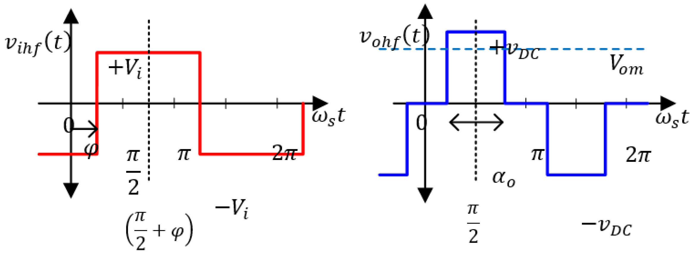
The DABSR DC-DC converter performs the average DC-link voltage control and the APD. For this purpose, the modulating signal presented in Figure 2 are as follows:
For the DC-source Active Bridge (AB):
s 1 = s g n sin ω s t φ ,
For the DC-link AB:
s 2 = s g n cos ω s t α o 2 s 3 = s g n cos ω s t + α o 2     ,
where ω s is the switching frequency, and the function s g n x is defined as:
s g n x = 1 ,           x 0 0 ,           x < 0   ,
The modulated voltages are shown in Figure 3. Note that two command signals are used: the duty ratio (DR) angle α o and the phase-shift (PS) angle φ . Hence, from the Fourier Series expansion, the fundamental components of the modulated voltages of Figure 3 can be expressed as presented in (6).
v i h f , 1 = 4 π V i sin ω s t φ v o h f , 1 = 4 π V o m sin ω s t                 ;   V o m = v d c sin α o 2
The time-variation of v d c can be considered constant during one switching period since   ω s 2 ω b , where ω b is the grid frequency. Note in (6) that V o m is affected by the DC-link voltage v d c , which is time-variant a cause of the high ripple Δ V d c , and the DR angle α o 2 . In the proposed modulation, the voltage V o m is controlled, in open loop, to have a constant value throughout the grid period.
On the other hand, with the aim of having high selectivity at the switching frequency ω s , the tank circuit inductance and capacitance, L r and C r are sized considering a high-quality factor Q 4 and a resonance frequency   ω r close to ω s ( ω s 1.1   ω r ) [38]. These parameters are defined as:
Q = Z 8 n 2 π 2 V i 2 P   ;             ω r = 1 L r C r ;           Z r = L r / C r ,
where Z r is the characteristic impedance of the tank circuit, n is the turns-ratio of the high frequency (HF) transformer, and P the nominal power.
To analyze the impact of LFR in the battery current, calculate the average input non-filtered current i i l f in the DABSR DC-DC converter (see Figure 2) in one switching period as follows:
i i l f = 1 2 π 0 2 π n i o h f × s 1   d ( ω s t ) ,
where s 1 is defined in (3). Since the LC filter on the battery side, shown in Figure 2, is sized to filter the switching frequency, then it is possible to make the equivalence I i i i l f . Solving (8), the battery current results in:
I I i i l f = K v d c sin α o 2 s i n φ = K V o m sin φ
where V o m is defined in (6), and the constant K given by:
K = 8 n π 2 Z F 1 / F ,           F = ω s ω r
On the other terminal, the average output non-filtered current i i l f (presented in Figure 2) is calculated in a similar way as for i i l f for one switching period, obtaining:
i o l f = I o φ sin α o 2 ,             I o φ = K o sin φ
In (11), K o = K V i , with K defined in (10), and V i is the DC source voltage. Additionally, the HF transformer turns-ratio is sized as:
n = V o m / V i ,
with the aim of matching the controlled voltage on the HF transformer secondary side V o m with the DC source V i . This minimizes the HF current in the series-resonant circuit, as will be explained in the control strategy in Section 4. The two-stage DC-AC converter elements are summarized in Table 2 for a 2 kW prototype.

3. DC-AC Control: Single-Phase GFM with Improved Stability

The proposed single-phase GFM control, implemented at the DC-AC stage, is designed in a per unit (p.u.) system [39]. As shown in Figure 4, this is organized in three main levels: the power-related control, the virtual impedance, and the inner inverter control [40].

3.1. Power-Related Control

The GFM control presented is intended to operate in both grid-tied and islanded modes, but this implies two different line impedances and therefore different dynamics. Nevertheless, as discussed in [30] for dual-loop-controlled GFM converters with an LCL output filter, the control bandwidth decoupling between AC voltage and power loops is worse in a grid-tied operation in comparison to an islanded operation. When the generic power-related control is designed considering the critical case, it means it is a grid-tied operation.
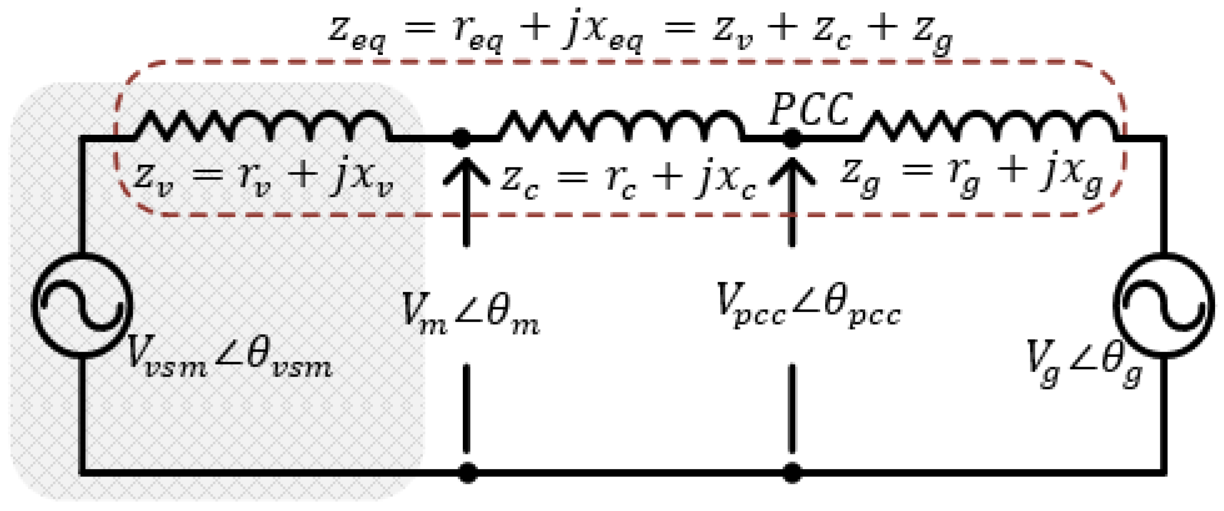
The circuit model for the grid-tied converter is shown in Figure 5, where the source V v s m θ v s m represents the VSM emf; V p c c θ p c c is the voltage in the PCC,]; V g θ g is the grid voltage; and z v ,   z c , and z g are the virtual impedance, the inverter filter impedance, and the grid impedance, respectively.
Considering an inductive line in Figure 5, the p.u. total reactance x e q = x g + x c + x v is much greater than the p.u. total resistance ( r g + r c + r v ) , where x c = ω b L 1 / Z b + ω b L 2 / Z b is the sum of the per unit filter reactances of the converter. If the power angle Δ θ = θ v s m θ g and the voltage difference V v s m V g are small, then the approximate expressions of the active and reactive power are as presented in (13) and (14), from which it can be seen that a mainly inductive line decouples the control of active and reactive power [41]:
P V v s m V g x e q Δ θ ,
Q V v s m V v s m V g x e q ,

3.1.1. Droop Control

According to the P-Q decoupling expressed in (13) and (14), frequency and amplitude droops are implemented as presented in (15) and (16), respectively, to enable parallel operation with other VSGs and SGs and load sharing (see Figure 4). At their outputs’ active power and reactive power control references, p o * and q o * are set according to the frequency and amplitude deviations in v p c c :
p o * = p o * * + k ω ω * + ω p c c ,
q o * = q o * * + k V V * + V p c c ,
where, p o * * , q o * * , ω * , and V * are the input references set by the charger’s user. According to the nominal power of the designed converter, it is established that it must provide frequency support by injecting 4.2% of its nominal power (in W) for every 0.1 Hz reduction in v p c c frequency, or by injecting 4.5% of its nominal power (in VAR) for every volt reduction in v p c c amplitude, similar to [31]. Thus, the droop gains 𝑘𝜔 and 𝑘𝑉 are set to 0.04 (4%) and 0.1 (10%), respectively.

3.1.2. Active Power Control

The mechanical part of the SM is implemented in a block that incorporates the small signal model of the swing equation, setting ω * = 1   p . u . as the frequency operation point as shown in Figure 4 [34]. Directly from Newton’s second law for rotary motion that relates the electrical and mechanical torque in a SM, results of the swing equation are expressed in terms of electrical and mechanical powers:
ω r = 1 2 H   s p o * p o k d ω r ω p c c ,
where ω r represents the angular frequency of the SM rotor in electrical rad/s, H is the inertia constant, and k d is the damping factor for a frequency deviation in the PCC.
For active power control (APC), the PLL-free grid forming presented in [35] is taken as reference, since it allows the tuning of its parameters setting a desired bandwidth, based on a second order model of the equivalent simplified swing equation:
ω v s m = 1 2 H   s p o * p o k p p o ,
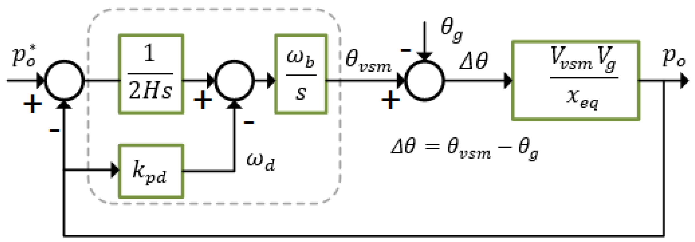
For tuning effects, the simplified swing equation model is treated as an IP controller. For a plant based on an approximation of the power sharing dependent on the angle difference Δ θ in the two-source converter-grid model [35], this is shown in Figure 6.
According to Figure 6 and considering that the grid frequency is practically constant, the second order model for the active power is given by:
p o s p o * s = 1 2 H   x e q ω b s 2 + 2 H k p s + 1 ,
for the second-order system presented in (19), the following design conditions are established: bandwidth B W P = 2 π 5   rad / s and damping coefficient ζ = 0.7 .

3.1.3. Reactive Power Control

For reactive power control (RPC), PI controller is used, which offers a stiff regulation of the reference voltage amplitude to get a certain desired reactive power [42]. Like APC, the plant for the linear model results from the approximation of the reactive power flow in inductive lines for the two-source converter-grid model, but in this case, considering the impedances instead of only reactances, performs a zero-pole elimination for tuning the PI gains. For the plant model, the approximation of the nominal voltage presented in [42] is employed. Based on these considerations, the RPC loop is as shown in Figure 7.
The PI controller gains k p q and k i q are established to set an open-loop transfer function cutoff frequency with a similar speed than the active power, ω c q = 2 π 5   rad / s .

3.2. Virtual Impedance and Stability Improvement

The active and reactive power controllers are tuned based on a linearized static model of the AC system expressed in (13) and (14), which neglects the P-Q coupling under the condition that the transmission line between the two sources is mainly inductive ( X R ). To ensure that condition, a virtual impedance z v that emulates the stator impedance of a physical synchronous machine is implemented, generating a bandwidth reduction in power control. The virtual impedance produces a voltage drop in the VSM machine EMF ( v v s m ), then the reference voltage at the output of the virtual impedance block is:
v m = v v s m i c z v ;                 z v = r v + j ω v s m x v ,
To avoid noise amplification due to voltage drop in the virtual reactance requiring a derivative of the current, quasi-stationary approximation is employed, as described in [43], using the quadrature current i c , β from the power measurement block. In that way, the output reference voltage results in:
v m = v v s m i c r v + ω v s m i o , β x v ,
A typical reactance value of 0.3 p.u. is chosen for x v , as in a grid-connected synchronous machine [44]. To set and inductive stator impedance, virtual resistance is chosen following r v < x v / 5 .

Stability Improvement Using Transitory Virtual Resistance

Although the linear static model is a good approximation for Δ θ < 30 ° , it hides fast dynamics that can affect the stability of smaller AC systems. As explained in [45] for an AC system as the one shown in Figure 5, the dynamics analysis around the operation point reveals that the relations between the variation of the active and reactive powers ( Δ p o and Δ q o ), with respect to the amplitude and phase variations of the voltage at the output of the active bridge ( Δ V m and Δ θ m ), share the same second-order characteristic polynomial in Laplace domain:
Δ p o Δ q o = N 1 D s N 2 D s N 3 D s N 4 D s Δ θ m Δ V m ,
where N 1 ,   N 2 ,   N 3 and N 4 are second-order polynomials, and D s is the characteristic polynomial:
D s = x e q ω p c c s + r e q 2 + ω p c c x e q 2 ,  
the polynomial D s shows that the oscillatory modes of the converter-grid AC system are mainly dependent of the line impedance, whose damping coefficient is:
ζ A C = r e q r e q 2 + x e q ω p c c 2 ,
In the case that ζ A C results are too small that the system is prone to destabilization, then the addition of a virtual damping resistance r v d in series with the physical filter impedance may stabilize the AC system, damping the resonance peaks. Hence, the addition of r v d virtually in series with the filter resistance r c establishes a new characteristic polynomial D * s = x e q s / ω p c c + r e q + r v d 2 + ω p c c x e q 2 that allows the selection of a desired new damping value ζ A C * . Then the virtual damping resistance will be designed according to:
r v d = ζ A C * x e q ω p c c 1 ζ A C * 2 r e q ,
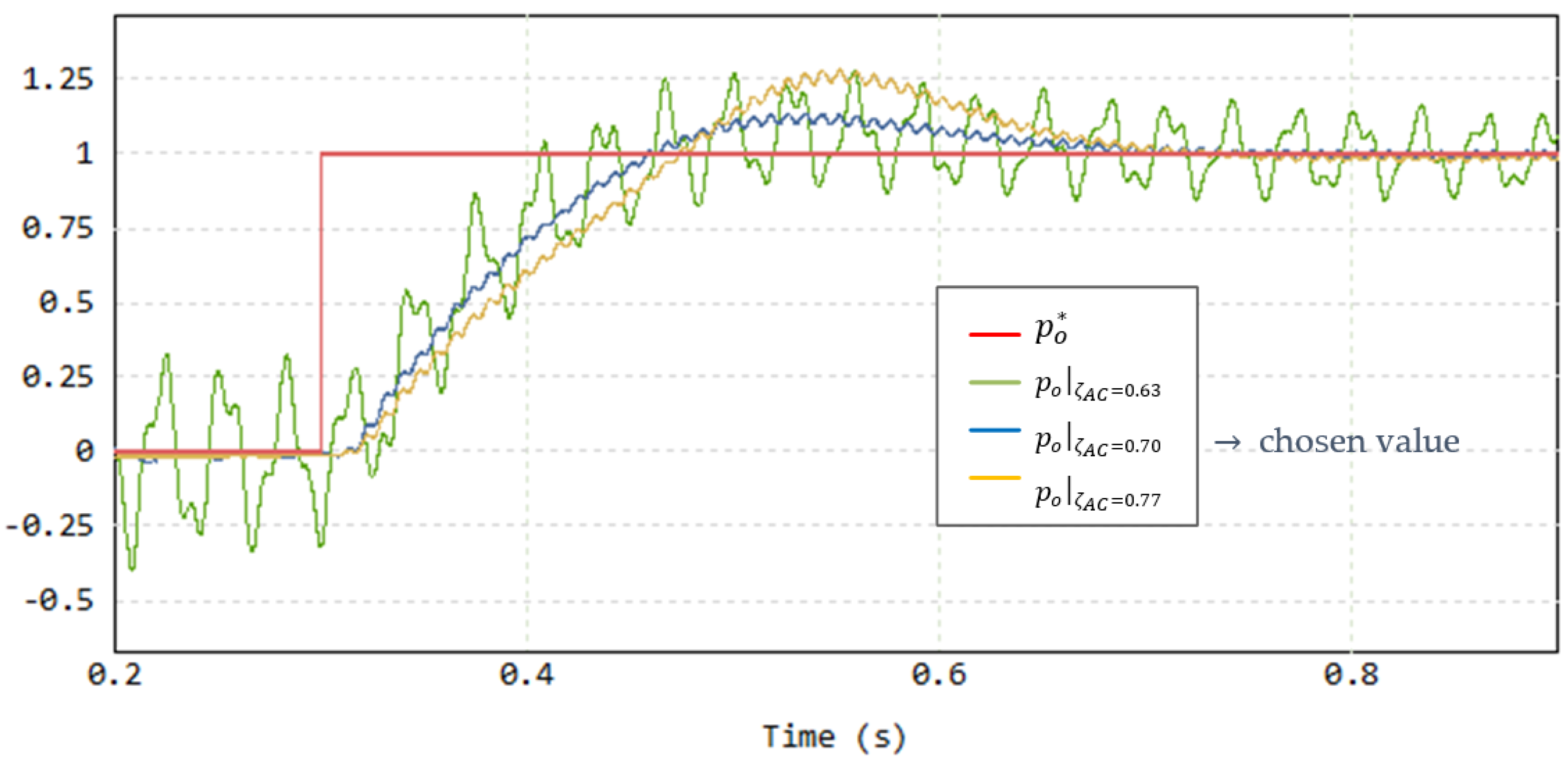
However, the addition of r v d affects the low-frequency response of the AC system, and therefore the model used by the P-Q controllers. To avoid this effect, a high-pass filter (HPF) must be added in series, conforming the Transitory Virtual Resistor (TVR) as shown in Figure 4, whose cutoff frequency must be less than the frequencies at which the AC system could resonate: ω c , H P F ω g / 2 [45]. The dynamics enhancement for three values of ζ A C in the grid-tied operation of the designed system is shown in the time-domain simulations presented in Figure 8. In islanded operation, the addition of the TVR improves the converter stability in low passive damping conditions, i.e., very low or no load is connected at the PCC.

3.3. Inner Inverter Control

The system is capable of operating without an inner inverter control, using directly v c * as the modulating signal in SPWM block. However, due to the use of small DC-link film capacitors, the high double-line frequency ripple (DLFR) in v d c leads to high THD in the current injected into the grid. This fact makes it advisable to use a dual loop control capable of attenuate the main harmonic components of the injected current. Therefore, a dual control loop of voltage and current is incorporated as the most internal loop, and therefore the fastest of the designed system. Its reference signal v c * comes from the TVR.
To reduce the sensors number, the smaller capacitance C f is chosen to approximate i c i o , and the voltage drop on the grid-side inductor is neglected allowing the approximation of v p c c v c .Then, the inner voltage controller gains are tuned considering the approximations for i o and v p c c , taking the filter capacitor C f as the plant and using the symmetrical optimum method to maximize the phase margin [34]. Then, the open-loop bandwidth set by the cutoff frequency ω c v = 10 ω b is chosen to calculate k p v and k r v , resulting in a phase margin equal to 59° for its open-loop transfer function. In addition, compensation feedforwards are added to enhance the signal tracking and to compensate external disturbances in both the voltage control loop and current control loop, as explained in [34].
The inner current control loop model is presented in Figure 9. However, for implementation, as shown in Figure 4, signal feedback ( i c ) can be bypassed since it is canceled by the compensation feedforward signal ( i o i c ), thus avoiding feeding back the signal with higher THD and related stability problems [30]. A multi-resonant controller P + R ω + R 3 ω is used to control i c and obtain zero error in a steady state [46]. This controller is chosen due to the high presence of the third harmonic, which appears due to the high DLFR in the DC-link. Given the DC-link voltage v d c t V d c + 0.5   Δ V d c cos ( 2 ω b t θ ) and the generated PWM voltage v m m v d c sin ω b t θ , where m is the modulation index, then the third harmonic appears as indicated in (26):
v m = m V d c sin ω b t θ + m Δ V d c 4 sin ω b t θ + m Δ V d c 4 cos 3 ω b t 2 θ ,
it can be appreciated that oscillations at ω b = 2 π 60   rad / s and at 3 ω b are noticeable and resonant controller at ω b and at 3 ω b are required to obtain zero error in steady-state response.
In Figure 9, R ω s and R 3 ω s are the resonant controllers centered at the frequencies ω b = 2 π 60 and 3 ω b , g P W M s represents the delay generated by modulation sampling, and the plant g l 1 s comes from the converter-side inductor. The tuning of the controller PR1 is performed with its equivalent PI controller in a synchronous reference frame [47,48] to get to a desired bandwidth. By performing a zero-pole elimination and setting a cutoff frequency ω c c = 5 ω c v , the controller gains k p c and k r are obtained.
Since the reference current given by the voltage controller has very low harmonic distortion, a resonant controller centered at 3 ω b is added to track/reject the third harmonic component in the AC output current. In this case, the gain k 3 r is selected equal to three times k r since it achieves a high gain in the peak at 3 ω b , without modifying the bandwidth and phase margin. The frequency response of the open loop transfer function for the inner current control loop g c c s is shown in Figure 10.
In Figure 9, the modulating signals are disabled while the synchronization process takes place with the signal ‘EN’. This action avoids integrator saturation and keeps the output voltage and current at zero during initialization.

4. DC-DC Control: DC-Link Control and Active Power Decoupling

In the proposed control strategy, the average DC-link voltage is controlled by the DC-DC converter and not by the DC-AC as is usual in GFO control strategies [20,49]. Therefore, the average DC-link voltage control along with the APD algorithm are shown in Figure 11.

4.1. Active Power Decoupling Based on DR Modulation

The expression (9) implies that if no power decoupling is performed and considering that sin φ does not present low frequency variations, the LFR on v d c will be reflected in the battery current I i . Hence, in the proposed APD, the DR angle α o / 2 changes in such a way that V o m takes a constant value in all the grid period. For this purpose, according to (6), the DR angle is calculated as follows:
α o 2 = sin 1 V o m v d c
which implies the restriction v d c V o m . Applying (27) in (9), the LFR of v d c will be canceled in the battery current I i since V o m is a set constant.
Furthermore, the HF current is expected to have a constant value amplitude throughout the grid period compared to systems that do not employ the proposed APD algorithm, since the voltage seen in the DC-link side by the resonant circuit is reduced to V o m . In that way, according to (6) and (27):
i o h f t = 4 π X r n V i cos ω s t φ V o m cos ω s t ,
where X r = X L r + X C r = Z o F 1 / F is the total reactance of the resonant circuit. Hence, from (28) the peak value of the HF current can be estimated according to:
I o h f ,   p k = 4 π X r V o m 2 + n V i 2 2 n V i V o m cos φ
The DC-link side power can be calculated as follows:
P o = v d c i o l f = K V i V o m sin φ ,
showing that, whenever sin φ is free of low-frequency ripple, the APD algorithm decouples the low-frequency oscillations in both DABSR terminals.

4.2. DC-Link Voltage Control

In the proposed control strategy, the average DC-link voltage V d c is controlled by the DABSR DC-DC converter. For this purpose, the average DC-link voltage model is shown in Figure 12, where i o l f is given by (11).
In Figure 12a, the VSI input current i d c has a low frequency component I o cos 2 ω g t and a DC component I o , which means:
i d c = I o + I o cos 2 ω g t ,  
where I o = V d c / R d c , whereas R d c = V d c 2 / P o ; R d c is the output load at nominal power P o , V d c is the average DC-link voltage, and C d c is the DC link capacitor. Then, according to (11) and (27), i o l f is given by:
i o l f = I o φ sin α o 2 = I o φ V o m v d c = I o φ V o m V d c 1 + 0.5 Δ V d c V d c c o s 2 ω g t ,  
where V o m is controlled by the DR angle α o according to (6), and V d c ,   Δ V d c are the averaged DC-link voltage and ripple, respectively. Hence, considering 1 0.5 Δ V d c / V d c , the DC component of i o l f , i o l f d c can be rewritten as:
i o l f d c = β I o φ ,           where   β = V o m V d c ,  
resulting in the average model of the average DC-link circuit shown in Figure 12b. Then, the plant transfer function employed for tuning the controller is:
V d c s I o φ s = β R d c 1 + R d c C d c s
With these considerations, the average DC-link voltage control diagram is shown in Figure 13. The notch-filter H N F s , centered at 2 ω g = 2 π 120   rad / s , is implemented with the aim of increasing the bandwidth of the PI controller [8]. For this model, it is required that the function sin φ in (11) does not present low-frequency variations. Then, if necessary, it is possible to add another notch-filter on the control signal I o φ . Nevertheless, consider that notch-filter limit the bandwidth of the PI controller to be less than 2 ω g .
According to Figure 13 the open-loop transfer function of the system is:
h d c s = k p 1 + T i s T i s β R d c 1 + R d c C d c s ,
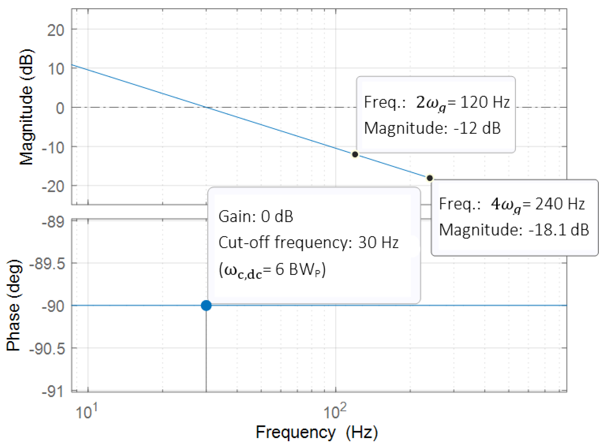
The controller gains k p and k i = k p / T i are determined by performing a zero-pole elimination to establish a chosen cut-off frequency of ω c , d c . Two criteria are used to select the cut-off frequency ω c , d c : inferiorly, to avoid interfering with transient stability, it must be much larger than the power control bandwidth B W P , since it is the loop with the slowest dynamics; and superiorly, due to the component 2 ω g being canceled by the notch-filter, it must be much smaller than the subsequent harmonic, 4 ω g . Hence, a proper relationship is achieved when:
5 B W P ω c , d c 4 ω g / 5
In the presented control strategy, it has been considered that ω c , d c = 6   B W P . Finally, since I o φ is linked to the PS φ according to (11), the control signal φ is calculated as:
φ = sin 1 I o φ K o
In Figure 14 the open-loop frequency response is presented. The controller parameters are summarized in Table 3.

5. Experimental Results Using Hardware-in-the-Loop

Experimental tests have been realized using Typhoon Hardware-in-the-Loop (HIL) 402 to emulate the electronic power circuit in real time, whereas the control was performed by Texas Instruments DSP F28335. The signals used in the control are scaled for digital processing before entering the ADC, whereas the internal control signals are scaled in a 12-bit DAC to have a good resolution when displayed on the oscilloscope. In summary, the scales of the signals shown in the graphs are presented in Table 4.
In Table 4, the scale 0.1 Hz/1V, for example, means that 1V ion the oscilloscope screen represents 0.1 Hz in real signal, and in the same way for the other signals.

5.1. Dynamic Response to Frequency Events

The transient response of active power, reactive power, and frequency of the designed system is shown in Figure 15, where p o * , p o , and q o are the signals employed in the control presented in Section 3, and Δ f p c c is the frequency deviation (in Hertz) in the PCC. It can be seen that p o develops a damped dynamic with 20% overshoot at the transitions from 0 p.u. to 1 p.u, in V2G operation, with a settling time of approximately 350   ms . Grid-to-vehicle (G2V) operation shows a more damped response with no overshoot and faster settling of around 250   ms since G2V mode has a different dynamic behavior than V2G mode [7]. It can be noticed there is no interference in the transient dynamics of p o and q o , since the power control bandwidth is distanced six times with respect to the DC-link voltage control.
On the other hand, frequency support and inertial response are tested in Figure 16, operating bidirectionally for events of step variations in the grid frequency Δ f g , and such frequency events can be realized by the advantage provided by the HIL device. Delivering power to the grid at 80% of nominal power, a step down of 0.5 Hz in grid frequency is tested, increasing the output power to its nominal value according to the 4% frequency droop gain with no overshoot and an approximate settling time of 150   ms . In the opposite direction, charging the battery at 80% of the nominal power, the step up of 0.5 Hz in grid frequency forces the battery to be charged at an extra 20% of power.
Reactive power support for amplitude deviations in the grid voltage are tested in Figure 17. On the left is the case of a 10% increase in the amplitude of the network voltage V g , forcing the absorption of 1 p.u. of reactive power by the converter according to the 10% voltage droop gain. Conversely, on the right, the case of a 10% decrease in the amplitude forces the injection of 1 p.u. of reactive power to support the grid.
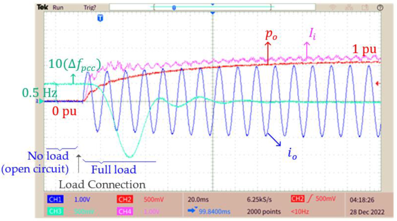
Figure 18 displays the transition from open circuit to full load that occurs when a load of 100% ( 24.2   Ω ) is connected at the output of the converter operating in islanded mode (stand-alone V2H mode). The transient response is faster than grid-tied operation as expected due to the missing of grid line impedance [30], with a settling time of 200   ms . To operate within the normal operating frequency band for small power systems, as mentioned in the network codes of Australia, China, or Great Britain [50], where a maximum frequency deviation of ± 0.5   Hz is allowed, for this stand-alone test the frequency droop gain is reduced to k ω = 0.83 % to get a maximum frequency deviation of 0.5   Hz if the difference between generation and demand is 1 p.u. However, it can be noted that for this test, the frequency reaches a minimum point of 48.5 Hz momentarily. Moreover, the frequency droop gain can be reduced if the maximum frequency deviation is ± 0.2   Hz , as in the European grid code [50]. Note that before load connection, the stability of the system relies on the active damping strategies implemented in the control system.

5.2. Power Decoupling Capability

The responses of the DC-link voltage with DC coupling ( v d c , red signal) and AC coupling ( Δ v d c , cyan signal) to a unit step in the reference power are shown in Figure 19a,b for DC-link capacitors of 240   μ F and 120   μ F , respectively, for testing the robustness of the designed system. Since in the second case the DC-link capacitor is halved, the PI gains change to maintain a bandwidth ω c , d c = 2 π 30   rad / s , while the DC-link ripple increases to double due to the DC-link film capacitor being reduced by half. The DC bus voltage stabilizes smoothly with an approximate settling time of 320   ms , in the presence of high LFR, as in Figure 19a, and very high LFR, as in Figure 19b. Since both tests are designed for the same bandwidth, the settling times are similar.
To illustrate the advantage of using the APD algorithm, the steady-state performance at nominal power using two different capacitors in the DC-link is compared in Figure 20. For the first case, the film capacitor of 240   μ F , and hence a high LFR ripple, is presented in the DC-link voltage. Meanwhile, the APD is performed by varying the DR angle α o according to (27) to decouple the single-phase power ripple. For the second case, an electrolytic capacitor of 1.2   mF is used, hence small LFR is presented in the DC-link, and the APD is removed, being α o = π / 2 .
Note in Figure 20a that the high DC-link voltage ripple Δ V d c is allowed to use a small film capacitor, but due to the APD the DC current I i and envelope amplitude of the HF current i o h f is quasi-constant. Because of the high DC-link ripple Δ V d c = 50   V , the average DC-link voltage is controlled to V d c = 450   V , and the APD is performed by the DR angle α o with the aim of obtaining V o m = 380   V for the resonant circuit, as presented in Figure 11. Conversely, in Figure 20b, the average DC-link voltage is controlled to V d c = 380   V with passive decoupling performed by a large DC-link capacitor, which is Δ V d c = 15   V small. Hence, according to (6) and (12), the series-resonant circuit and the HF transformer are identical for both cases. The PI controller would change according to the average DC link voltage and the DC-link capacitor. As a consequence, it is possible to compare their HF series-resonant circuit and battery currents, i o h f and I i , for both converters.
In Figure 20, for both cases the rated value of the average battery current I i is 4.6   A . For the film capacitor ( C d c = 240   μ F ) the peak-to-peak ripple in the battery current is Δ I i 0.4   A , which is 8.7 % of the rated average value. However, for the electrolytic capacitor ( C d c = 1.2   mF ) Δ I i 3.5   A , which is 75% of rated average value.
From Figure 20a, the peak value of the HF current is I o h f , p k 8.2   A , which is near to the expected value I o h f , p k = 8.5   A calculated by (29). In comparison, in Figure 20b the HF current gets a peak value I o h f , p k = 10.8   A . For the same DABSR design, the film capacitor with APD brings 5.2   A less peak-to-peak HF current than the electrolytic capacitor without APD, which implies reducing not only the DC-link capacitor volume but also the HF transformer and the resonant tank inductor volumes. Furthermore, in terms of electrical performance and lifetime, the film capacitor ( C d c = 240   μ F ) offers better characteristics than the electrolytic capacitors. It can be concluded that the proposed APD presents a notable performance, decreasing the HF current amplitude as well as the LFR on the DC current, and shows a better performance than the passive decoupling of an electrolytic capacitor with five times higher capacitance.
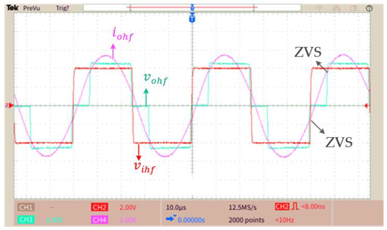
The ZVS mode is analyzed operating at nominal power in Figure 21, where high frequency AC voltages, produced by actives bridges, and the tank current are shown. For the V2G direction, ZVS is fulfilled in both active bridges according to the ZVS condition presented in (38). However, for the battery charging direction, ZVS mode can be lost in one leg if the DR angle α o takes small values.
i o h f > 0 ;       ω s t = π 2 α o 2 i o h f < 0 ;       ω s t = φ                
From the graphical results of Figure 21, a phase shift φ 27 ° is measured, which agrees with the estimated phase shift based on the calculation using (30).

6. Comparison with Previous Works

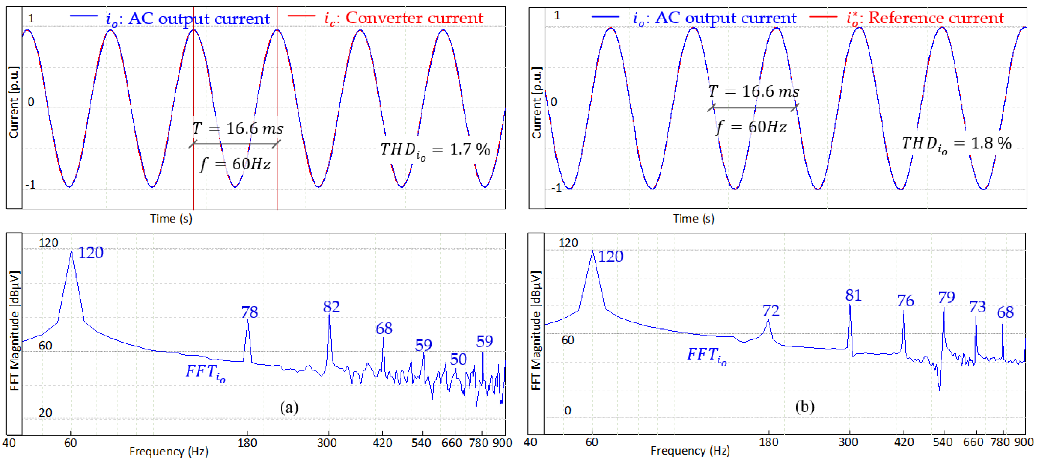
With the aim of comparing the GFM and the GFO performances with respect to the THD in the current injected into the grid, the GFO control strategy presented in [20] was set up using the same power circuit presented in Figure 2 to compare using simulation software. For both cases, the analysis has been done using a critical film capacitor C d c = 120   μ F in the DC-link. For its current controller, a multi-resonant controller P+R1+R3 is also implemented, like the inner current control loop presented in Figure 4.
Comparing Figure 22a with Figure 22b, it can be noticed that the THD of the current injected to the grids is quite similar, near to 1.8%. Note that the harmonics distributions are quite different between both control strategies. This is because in a GFO control the grid current reference comes from the v d c control loop [8], unlike the GFM control where the grid current reference comes filtered from the virtual impedance and the low-frequency power loop.
Therefore, it is shown that the GFM strategy can be implemented in a two-stage DC-AC with high ripple in the DC-link, obtaining similar grid current performances than GFO control strategies. The results obtained are relevant because it is known that the GFM control strategies performs better in weak grid conditions [25] and, due to their behave as controlled voltage sources, they can operate stand-alone to provide V2H services, unlike the GFO control strategies which behave like controlled current sources [27].
Finally, with the aim of highlighting the proposed converter and control strategy for SBC, a brief comparison with other DC-AC structures is presented in Table 5.
In [2], a control strategy for SBC is presented using a DC-DC composed of a bidirectional Boost converter DC-linked by electrolytic capacitors with a VSI. For this structure, V2G and stand-alone V2H have been reported in the literature. However, it does not have galvanic isolation and suffers from limited durability due to the use of electrolytic capacitors. Galvanic isolation is added used a DC-DC DAB in [7]. However, it has the same drawback of having limited durability by the usage of electrolytic capacitors in the DC-link. With the aim of increasing the converter durability, a similar structure of the proposed converter, using film capacitors in the DC-link, is presented in [20]. However only active power support for V2G services is reported. This structure has the drawback of having the double control loop DC-link voltage–grid current for the VSI, which can increase the THD in the grid current, since the grid current reference comes from the DC-link voltage loop, which has a high DC-link ripple [8]. Finally, a two-stage DC-AC converter with a different isolated DC-DC structure is presented in [22] for fuel cell applications, but only stand-alone control is presented. Therefore, with the previous comparison, the proposed DC-AC converter is a good candidate for single-phase SBC, because it integrates V2G and stand-alone V2H capability in a unified GFM control strategy that offers high-quality power in its terminals, with the additional advantages of having galvanic isolation and high durability.

7. Conclusions

In this paper, a PLL-free single-phase GFM control strategy with active power decoupling for an isolated and bidirectional two-stage DC-AC converter considering high DC-link voltage ripple due to the use of film capacitors is presented. For a simplified tuning of the controllers, a distinction is made between low, medium, and high-speed controllers. The single-phase GFM control is tuned to operate with damped behavior against strong ripple from the DC link and low damping situations, such as when feeding small loads in stand-alone mode and avoiding the bandwidth coupling between their loops and with the DC-DC control. The active power decoupling, galvanic isolation, and soft switching features are combined with the grid forming characteristic to bring V2G and stand-alone V2H services. The proposed GFM strategy, average DC-link voltage control, and active power decoupling have been validated for grid events and stand-alone operation. The grid current of the proposed single-phase GFM control has been compared with an equivalent GFO control using the same power circuit. Results show that similar performances in the grid current THD are obtained. The results obtained are relevant because it is known that the GFM control strategies perform better in weak grid conditions and can operate stand-alone to provide V2H services, unlike the GFO control strategies. On the other hand, the proposed APD along with the average DC-link voltage control has been validated for different capacitance values in the DC-link. Results show that the proposed APD suppresses the LFR in the battery current as well as reduces the HF tank current amplitude in comparison with the typical passive power decoupling using electrolytic capacitors. ZVS mode is obtained by allowing high efficiency in the DABSR DC-DC converter. The proposed control strategy has been compared with similar structures, showing better features. Hence, the proposed converter along with the single-phase GFM strategy can be implemented in SBCs for V2G and stand-alone V2H applications. Finally, it is important to highlight that the proposed converter may work for unbalanced three-phase systems, which will be validated in future works.

Author Contributions

D.S.y.R. and A.Z. contributed to the research, investigation, results analysis, resources, and writing—review and editing. All authors have read and agreed to the published version of the manuscript.

Funding

This research was supported by Concytec-Prociencia by the project “Manufactura Avanzada de Estaciones de recarga rápida de vehículos eléctricos basada en Sistemas Fotovoltaicos Inteligentes” [Contract N° 007-2021].

Data Availability Statement

All the reported data are included in the manuscript.

Conflicts of Interest

The authors declare no conflict of interest.

References

  1. Hu, Q.; Bu, S.; Terzija, V. A Distributed P and Q Provision-Based Voltage Regulation Scheme by Incentivized EV Fleet Charging for Resistive Distribution Networks. IEEE Trans. Transp. Electrif. 2021, 7, 2376–2389. [Google Scholar] [CrossRef]
  2. Restrepo, M.; Morris, J.; Kazerani, M.; Cañizares, C.A. Modeling and Testing of a Bidirectional Smart Charger for Distribution System EV Integration. IEEE Trans. Smart Grid 2018, 9, 152–162. [Google Scholar] [CrossRef]
  3. Monteiro, V.; Pinto, J.G.; Afonso, J.L. Operation Modes for the Electric Vehicle in Smart Grids and Smart Homes: Present and Proposed Modes. IEEE Trans. Veh. Technol. 2016, 65, 1007–1020. [Google Scholar] [CrossRef] [Green Version]
  4. Monteiro, V.; Exposto, B.; Ferreira, J.C.; Afonso, J.L. Improved Vehicle-to-Home (iV2H) Operation Mode: Experimental Analysis of the Electric Vehicle as Off-Line UPS. IEEE Trans. Smart Grid 2017, 8, 2702–2711. [Google Scholar] [CrossRef] [Green Version]
  5. Sfakianakis, G.E.; Everts, J.; Lomonova, E.A. Overview of the requirements and implementations of bidirectional isolated AC-DC converters for automotive battery charging applications. In Proceedings of the Ecological Vehicles and Renewable Energies (EVER) Conference, Monte Carlo, Monaco, 31 March–2 April 2015. [Google Scholar]
  6. Zhang, Y.; Fang, J.; Gao, F.; Gao, S.; Rogers, D.J.; Zhu, X. Integrated High- and Low-Frequency Current Ripple Suppressions in a Single-Phase Onboard Charger for EVs. IEEE Trans. Power Electron. 2021, 36, 1717–1729. [Google Scholar] [CrossRef]
  7. Iyer, V.M.; Gulur, S.; Bhattacharya, S. Small-Signal Stability Assessment and Active Stabilization of a Bidirectional Battery Charger. IEEE Trans. Ind. Appl. 2019, 55, 563–574. [Google Scholar] [CrossRef]
  8. Gautam, A.R.; Fulwani, D.M.; Makinen, R.R.; Rathore, A.K.; Singh, D. Control Strategies and Power Decoupling Topologies to Mitigate 2ω-Ripple in Single Phase Inverters: A Review and Open Challenges. J. IEEE Access 2020, 8, 147533–147559. [Google Scholar] [CrossRef]
  9. Sun, Y.; Liu, Y.; Su, M.; Xiong, W.; Yang, J. Review of Active Power Decoupling Topologies in Single-Phase System. IEEE Trans. Power Electron. 2016, 31, 4778–4794. [Google Scholar] [CrossRef]
  10. Liu, Y.; Zhang, W.; Sun, Y.; Su, M.; Xu, G.; Dan, H. Review and Comparison of Control Strategies in Active Power Decoupling. IEEE Trans. Power Electron. 2021, 36, 14436–14455. [Google Scholar] [CrossRef]
  11. Wang, H.; Wang, H.; Zhu, G.; Blaabjerg, F. An Overview of Capacitive DC-Links-Topology Derivation and Scalability Analysis. IEEE Trans. Power Electron. 2020, 35, 1805–1829. [Google Scholar] [CrossRef]
  12. Kisacikoglu, M.C.; Kesler, M.; Tolbert, L.M. Single-Phase On-Board Bidirectional PEV Charger for V2G Reactive Power Operation. IEEE Trans. Smart Grid 2015, 6, 767–775. [Google Scholar] [CrossRef]
  13. De Melo, H.N.; Trovao, J.P.F.; Pereirinha, P.G.; Jorge, H.M.; Antunes, C.H. A Controllable Bidirectional Battery Charger for Electric Vehicles with Vehicle-to-Grid Capability. IEEE Trans. Veh. Technol. 2018, 67, 114–123. [Google Scholar] [CrossRef]
  14. Kazemtarghi, A.; Dey, S.; Mallik, A. Optimal Utilization of Bidirectional EVs For Grid Frequency Support in Power Systems. IEEE Trans. Power Deliv. 2022, 1–13. [Google Scholar] [CrossRef]
  15. Zhang, Z.; Liu, B.; Song, S. Power Decoupling Control for V2G/G2V/PV2G Operation Modes in Single-Phase PV/Battery Hybrid Energy System with Low DC Link Capacitance. J. IEEE Access 2021, 9, 160975–160986. [Google Scholar] [CrossRef]
  16. Xu, J.; Soeiro, T.B.; Gao, F.; Tang, H.; Bauer, P. Minimum Switching Losses Discontinuous PWM Strategy for Bidirectional Single-Phase AC–DC Converter with Active Power Decoupling. IEEE Trans. Power Electron. 2021, 36, 6118–6132. [Google Scholar] [CrossRef]
  17. Sal y Rosas, D.; Frey, D.; Schanen, J.-L.; Ferrieux, J.-P. Isolated Single Stage Bidirectional AC-DC Converter with Power Decoupling and Reactive Power Control to Interface Battery with the Single-Phase Grid. In Proceedings of the 2018 IEEE Applied Power Electronics Conference and Exposition (APEC), San Antonio, TX, USA, 4–8 March 2018; 2018; pp. 631–636. [Google Scholar] [CrossRef]
  18. Patil, D.; Agarwal, V. Compact Onboard Single-Phase EV Battery Charger with Novel Low-Frequency Ripple Compensator and Optimum Filter Design. IEEE Trans. Veh. Technol. 2016, 65, 1948–1956. [Google Scholar] [CrossRef]
  19. Nguyen, H.V.; To, D.-D.; Lee, D.-C. Onboard Battery Chargers for Plugin Electric Vehicles with Dual Functional Circuit for Voltage Battery Charging and Active Power Decoupling. J. IEEE Access 2018, 6, 70212–70222. [Google Scholar] [CrossRef]
  20. Pantaleon, E.; y Rosas, D.S.; Espinoza, R. Modulation and Control Strategy for an isolated and bidirectional two-stage DC-AC converter with high ripple on the DC-Link to interface battery with the single-phase grid. In Proceedings of the PEDG Conference, Chicago, IL, USA, 28 June–1 July 2021. [Google Scholar]
  21. Liu, B.; Li, G.; He, D.; Chen, Y. DC and AC Power Quality Control for Single-Phase Grid-Tied PEMFC Systems with Low DC-Link Capacitance by Solution-Space-Reduced MPC. IEEE Trans. Ind. Electron. 2022, 69, 5625–5636. [Google Scholar] [CrossRef]
  22. Liu, X.; Li, H. An Electrolytic-Capacitor-Free Single-Phase High-Power Fuel Cell Converter with Direct Double-Frequency Ripple Current Control. IEEE Tran. Ind. Appl. 2015, 51, 297–308. [Google Scholar] [CrossRef]
  23. Meng, L.; Shu, Z.; Lei, Y.; Yan, H.; Li, Z.; Ma, L.; Yin, X.; He, X. Optimal Input and Output Power Quality Control of Single-Phase AC–DC–DC Converter with Significant DC-Link Voltage Ripple. IEEE Trans. Ind. Electron. 2020, 67, 10366–10376. [Google Scholar] [CrossRef]
  24. Lasseter, R.H.; Chen, Z.; Pattabiraman, D. Grid-Forming Inverters: A Critical Asset for the Power Grid. IEEE J. Emerg. Sel. Top. Power Electron. 2020, 8, 925–935. [Google Scholar] [CrossRef]
  25. Zhang, H.; Xiang, W.; Lin, W.; Wen, J. Grid Forming Converters in Renewable Energy Sources Dominated Power Grid: Control Strategy, Stability, Application, and Challenges. J. Mod. Power Syst. Clean Energy 2021, 9, 1239–1256. [Google Scholar] [CrossRef]
  26. Rathnayake, D.B.; Akrami, M.; Phurailatpam, C.; Me, S.P.; Hadavi, S.; Jayasinghe, G.; Zabihi, S.; Bahrani, B. Grid Forming Inverter Modeling, Control, and Applications. J. IEEE Access 2021, 9, 114781–114807. [Google Scholar] [CrossRef]
  27. Rosso, R.; Wang, X.; Liserre, M.; Lu, X.; Engelken, S. Grid Forming Converters: Control Approaches, Grid-Synchronisation and future Trends-A Review. IEEE Open J. Ind. Appl. 2021, 2, 93–109. [Google Scholar] [CrossRef]
  28. Kwon, M.; Park, S.; Oh, C.-y.; Lee, J.; Choi, S. Unified Control Scheme of Grid-Connected Inverters for Autonomous and Smooth Transfer to Stand-Alone Mode. IEEE Trans. Power Electron. 2022, 37, 416–425. [Google Scholar] [CrossRef]
  29. Liu, J.; Miura, Y.; Bevrani, H.; Ise, T. A Unified Modeling Method of Virtual Synchronous Generator for Multi-Operation-Mode Analyses. IEEE J. Emerg. Sel. Top. Power Electron. 2021, 9, 2394–2409. [Google Scholar] [CrossRef]
  30. Deng, H.; Fang, J.; Qi, Y.; Tang, Y.; Debusschere, V. A Generic Voltage Control for Grid-Forming Converters with Improved Power Loop Dynamics. IEEE Trans. Ind. Electron. 2022, 1–13. [Google Scholar] [CrossRef]
  31. Suul, J.A.; D’Arco, S.; Guidi, G. Virtual Synchronous Machine-Based Control of a Single-Phase Bi-Directional Battery Charger for Providing Vehicle-to-Grid Services. IEEE Trans. Ind. Appl. 2016, 52, 3234–3244. [Google Scholar] [CrossRef] [Green Version]
  32. Ashtiani, N.A.; Khajehoddin, S.A.; Karimi-Ghartemani, M. Modeling and Stability Analysis of Single-Phase Microgrids Controlled in Stationary Frame. IEEE Trans. Power Electron. 2022, 37, 7759–7774. [Google Scholar] [CrossRef]
  33. Karimi-Ghartemani, M.; Sharma, R.; Zakerian, A.; Khajehoddin, S.A. A Single-phase Enhanced Grid-forming Controller with Converter Current Limiting. In Proceedings of the ECCE Conference, Vancouver, BC, Canada, 10–14 October 2021. [Google Scholar]
  34. Zarate, A.; Peña, J.C.U.; y Rosas, D.S. Isolated and Bidirectional two-stage DC/AC converter with grid-forming virtual inertia and high ripple on the DC bus for Single-Phase Grid applications. In Proceedings of the PEDG 2021, Chicago, IL, USA, 28 June–1 July 2021. [Google Scholar]
  35. Qoria, T.; Rokrok, E.; Bruyere, A.; Francoi, B.; Guillaud, X. A PLL-Free Grid-Forming Control with Decoupled Functionalities for High-Power Transmission System Applications. IEEE Access J. 2020, 8, 197363–197378. [Google Scholar] [CrossRef]
  36. Ruan, X.; Wang, X.; Pan, D.; Yang, D.; Li, W.; Bao, C. Control Techniques for LCL-Type Grid-Connected Inverters; CPSS Power Electronics Series; Springer: Singapore, 2018. [Google Scholar] [CrossRef]
  37. IEEE Standards Coordinating Committee. In IEEE Standard for Interconnection and Interoperability of Distributed Energy Resources with Associated Electric Power Systems Interfaces; IEEE: Piscataway, NJ, USA, 2018. [CrossRef]
  38. Li, X.; Bhat, A.K.S. Analysis and Design of High-Frequency Isolated Dual-Bridge Series Resonant DC/DC Converter. IEEE Trans. Power Electron. 2010, 25, 850–862. [Google Scholar] [CrossRef]
  39. Kundur, P. Power System Stability and Control; Balu, N.J., Ed.; McGraw-Hill: New York, NY, USA, 1994. [Google Scholar]
  40. Dokus, M.; Mertens, A. On the Coupling of Power-Related and Inner Inverter Control Loops of Grid-Forming Converter Systems. IEEE Access 2021, 9, 16173–16192. [Google Scholar] [CrossRef]
  41. Laaksonen, H.; Saari, P.; Komulainen, R. Voltage and Frequency Control of Inverter Based Weak LV Network Microgrid. In Proceedings of the 2005 International Conference on Future Power Systems, Amsterdam, The Netherlands, 18 November 2005; p. 6. [Google Scholar] [CrossRef]
  42. Taul, M.G.; Wang, X.; Davari, P.; Blaabjerg, F. Current Limiting Control with Enhanced Dynamics of Grid-Forming Converters During Fault Conditions. IEEE J. Emerg. Sel. Top. Power Electron. 2020, 8, 1062–1073. [Google Scholar] [CrossRef] [Green Version]
  43. Matas, J.; Castilla, M.; de Vicuna, L.G.; Miret, J.; Vasquez, J.C. Virtual Impedance Loop for Droop-Controlled Single-Phase Parallel Inverters Using a Second-Order General-Integrator Scheme. IEEE Trans. Power Electron. 2010, 25, 2993–3002. [Google Scholar] [CrossRef]
  44. Rodriguez, P.; Candela, I.; Citro, C.; Rocabert, J.; Luna, A. Control of Grid-Connected Power Converters Based on a Virtual Admittance Control Loop. In 2013 15th European Conference on Power Electronics and Applications (EPE); Lille, France, 2–6 September 2013, 2013. [Google Scholar] [CrossRef]
  45. Qoria, T. Grid-Forming Control to Achieve a 100% Power Electronics Interfaced Power Transmission Systems. Ph.D. Thesis, HESAM Université, Paris, France, 2020. [Google Scholar]
  46. Pereira, L.F.A.; Flores, J.V.; Bonan, G.; Coutinho, D.F.; da Silva, J.M.G. Multiple Resonant Controllers for Uninterruptible Power Supplies—A Systematic Robust Control Design Approach. IEEE Trans. Ind. Electron. 2014, 61, 1528–1538. [Google Scholar] [CrossRef]
  47. Zmood, D.N.; Holmes, D.G.; Bode, G.H. Frequency-Domain Analysis of Three-Phase Linear Current Regulators. IEEE Trans. Ind. Appl. 2001, 37, 601–610. [Google Scholar] [CrossRef]
  48. Teodorescu, R.; Blaabjerg, F.; Liserre, M.; Loh, P.C. Proportional-Resonant Controllers and Filters for Grid-Connected Voltage-Source Converters. IEE Proc.-Electr. Power Appl. 2006, 153, 750–762. [Google Scholar] [CrossRef] [Green Version]
  49. Yang, Z.; Zeng, J.; Yu, D.; Zhang, Q.; Zhang, Z. Two-Stage Power Decoupling for a Single-Phase Photovoltaic Inverter by Controlling the DC-Link Voltage Ripple in the DQ Frame. In Proceedings of the 2020 IEEE Applied Power Electronics Conference and Exposition (APEC), New Orleans, LA, USA, 15–19 March 2020. [Google Scholar] [CrossRef]
  50. Fang, J.; Li, H.; Tang, Y.; Blaabjerg, F. On the Inertia of Future More-Electronics Power Systems. IEEE J. Emerg. Sel. Top. Power Electron. 2019, 7, 2130–2146. [Google Scholar] [CrossRef]
Figure 1. Instantaneous power for single-phase two-stage DC-AC converter.
Energies 16 00894 g001
Figure 2. Two-stage DC-AC charger structure and control overview.
Energies 16 00894 g002
Figure 3. DABSR DC-DC converter modulated voltages.
Energies 16 00894 g003
Figure 4. Proposed single-phase GFM control with improved dynamic response.
Energies 16 00894 g004
Figure 5. Model of VSM connected to the grid by a mainly inductive line.
Energies 16 00894 g005
Figure 6. Block diagram for APC tuning.
Energies 16 00894 g006
Figure 7. Block diagram for RPC tuning.
Energies 16 00894 g007
Figure 8. Active power response for 1 p.u. step under three different damping ζ A C conditions.
Energies 16 00894 g008
Figure 9. Inner current loop control strategy.
Energies 16 00894 g009
Figure 10. Bode diagram of current control open-loop transfer function g c c s . Same bandwidth for P+R1 controller (blue), and for P+R1+R3 controller (red).
Energies 16 00894 g010
Figure 11. DC-DC average v d c control with active power decoupling.
Energies 16 00894 g011
Figure 12. DC-link model: (a) Model considering the high LFR, (b) Average model with APD.
Energies 16 00894 g012
Figure 13. Simplified control block diagram of the average DC-link voltage control.
Energies 16 00894 g013
Figure 14. Bode diagram of V d c control open-loop transfer function.
Energies 16 00894 g014
Figure 15. Response of p o ,   q o and Δ f p c c to a 100% step for (a) V2G, and (b) G2V operation.
Energies 16 00894 g015
Figure 16. Active power support in cases of grid frequency deviation of: (a) 0.5 Hz step down operating at 0.8 p.u., and (b) −0.5 Hz step up operating at −0.8 p.u.
Energies 16 00894 g016
Figure 17. Reactive power support in cases of grid voltage amplitude deviation of: (a) 10% step up, and (b) 10% step down.
Energies 16 00894 g017
Figure 18. Islanded operation to provide stand-alone services in full load range considering a maximum frequency deviation of ± 0.5   Hz .
Energies 16 00894 g018
Figure 19. Transient response in the battery current ( I i ), DC-link ( v d c and Δ v d c )for unit step in p o * . Comparison for C d c : (a) 240   μ F and (b) 120   μ F , critical case.
Energies 16 00894 g019
Figure 20. Comparison in I i and i o h f envelope (a) Using APD algorithm with C d c = 240   μ F , (b) Removing APD, only passive decoupling with C d c = 1.2   mF . Both with the same HF transformer and series-resonant circuit.
Energies 16 00894 g020
Figure 21. DC-DC ZVS at nominal power operating in V2G.
Energies 16 00894 g021
Figure 22. AC output current i o in time and frequency comparison using identical power circuit with different control strategies: (a) Proposed GFM and (b) GFO control strategy from [20].
Energies 16 00894 g022
Table 1. DC Link comparison for passive decoupling considering S o = 2   kVA and ω g = 2 π 60 .
ParameterDC Link Capacitance Value Capacitor Technology
V d c = 380   V ;   Δ V d c = 3 %
C d c = 1.2   mF
Electrolytic
V d c = 450   V ;   Δ V d c = 11 %
C d c = 240   μ F
Filmic
Table 2. Converter parameters.
SymbolParameter DescriptionValue
S b Nominal apparent power 2000   VA
V b Nominal RMS voltage 220   V
ω b Nominal grid angular frequency 2 π 60   rad / s
f s VSI and DAB switching frequency 20   kHz
L 1 ,   C f ,   L 2 LCL filter elements values 2   mH , 4.7   μ F ,   0.3   mH
L g Grid infinite bus model inductance 1.5   mH
C d c DC-link film capacitance 240   μ F
Δ V d c Peak-to-peak DC-link voltage ripple 50   V
V d c Average DC-link voltage 450   V
V o m Minimum DC-link voltage 380   V
Q Series-resonant circuit quality factor 4
L r ,   C r Series-resonant circuit elements values 1800   μ H ,   39 nF
n HF transformer turns-ratio 380 / 400
L i ,   C i Battery filter 0.5   mH ,   120   μ F
V i Battery voltage 400   V
Table 3. Controller parameters.
SymbolQuantityValue
k p c ,   k r ,   k 3 r PRR current controller gains 1.56 ,   58.7 ,   176 .2
k p v ,   k r v PR voltage controller gains 0.456 ,   324.2
r v ,   x v Virtual resistance and reactance 0.33 ,   0.066
r v d ,   ω c , H P F TVR and cut-off frequency 0.3 ,   75.4   rad / s
k ω ,   k V Frequency and amplitude droop gains 4 % ,   10 %
H ,   k p Inertia constant and damping factor 0.3452 ,   0.0530
k p q ,   k i q Reactive power controller gains 0.0324 ,   2.2594
k p ,   k i DC-link voltage controller gains 0.0452 ,   1.8617
B W P APC bandwidth 2 π 5 rad/s
B W d c DC-link voltage control bandwidth 2 π 30 rad/s
Table 4. Units and scales of signals plotted in oscilloscope.
SymbolValue
p o * ,   p o ,   q o 1 p.u./V
Δ f p c c ,   Δ f g 0.1 Hz/V
v d c ,   Δ v d c 100 V/V
v i h f ,   v o h f 100 V/V
i o h f 3 A/V
I i 2 A/V
i o 3.2141 A/V
Table 5. Proposed converter comparison with others two-stage DC-AC converter.
ParametersProposed
Converter
Non-Isolated DC-AC
[2]
Isolated
DC-AC
[7]
Isolated
DC-AC [20]
Isolated
DC-AC [22]
StructureDC-DC
DABSR + VSI
Bidirectional Boost + VSIDC-DC
DAB + VSI
DC-DC
DABSR + VSI
DC-DC
Three-phase DAB + VSI
DC-Link
Capacitor
FilmElectrolyticElectrolyticFilmFilm
DC-Link
Ripple
High (10%)Low (3%)Low (3%)High (10%)High (10%)
Galvanic
Isolation
YesNonYesYesYes
DurabilityHighLowLowHighHigh
Control
Strategy
V2G and Stand-Alone V2H in Unified
GFM strategy
V2G (GFO),
Stand-Alone AC Voltage
Control (V2H)
Only active power V2G
Reported
(GFO)
Only active power V2G
Reported
(GFO)
Only stand-alone AC voltage control reported
Disclaimer/Publisher’s Note: The statements, opinions and data contained in all publications are solely those of the individual author(s) and contributor(s) and not of MDPI and/or the editor(s). MDPI and/or the editor(s) disclaim responsibility for any injury to people or property resulting from any ideas, methods, instructions or products referred to in the content.