Article

High Step-Up Boost-Cuk-Forward Converter with Reduced Switch Voltage Stress and Ripple-Free Input Current

1
Mechatronics Engineering Department, Kyungsung University, Busan 48434, Republic of Korea
2
Electrical Engineering Department, University of Isfahan, Isfahan 8174673441, Iran
3
Electrical and Computer Engineering Department, Isfahan University of Technology, Isfahan 8415683111, Iran
*
Author to whom correspondence should be addressed.
Energies 2023, 16(17), 6391; https://doi.org/10.3390/en16176391
Submission received: 31 July 2023 / Revised: 30 August 2023 / Accepted: 31 August 2023 / Published: 3 September 2023
(This article belongs to the Section F3: Power Electronics)

Abstract

:
A new combined boost-Cuk-forward (CBCF) converter with ripple-free input current and low switch voltage stress is proposed for high step-up applications. Two coupled inductors are applied to achieve low switch voltage stress as well as balanced dc-link voltages, wherein the former is placed in series with the boost diode, and the latter is formed as a forward converter. Because these inductors are coupled with the output Cuk inductor, a ripple-free input current is also attained. The proposed converter is run at discontinuous conduction mode (DCM) by applying a low output-side Cuk inductance to reduce the switching loss by providing a ZCS turn-on of MOSFET and removing the diode reverse recovery current. In addition, the proposed converter does not have a problem with ground leakage current. The practical results verify the performance and effectiveness of the proposed CBCF high step-up converter.

1. Introduction

Nowadays, renewable energy source usage is fundamental to producing electricity since, unlike fossil fuels, they do not contaminate the environment and do not have negative effects on creatures’ lives. Among the renewable energy sources, solar panels have played a significant role owing to their accessibility throughout the world [1,2,3].
The terminal voltage of the photovoltaic (PV) cells is low. Various techniques have been presented to achieve an appropriate voltage level. Series connection of PV modules has been introduced for a string inverter; nonetheless, the MPPT attainment for each module is unfeasible in series connection [4,5]. The microinverter with a single PV module is the best method to achieve MPPT efficiently. As already mentioned, the terminal voltage of almost all renewable energy systems is low, and therefore, high step-up (HSU) dc–dc converters are vital to provide sufficient voltage for the dc-load or grid-tied inverters [2,3]. For instance, the dc-link voltage for the half-bridge inverter must be higher than twice the maximum grid voltage to transfer pure sinusoidal power to the network; otherwise, a distortion occurs at the peak point of the injected current due to a lack of sufficient voltage level.
In general, control-based [6] and topology-based [7,8,9,10,11,12] HSU converters have attracted much attention among scholars. Designing a highly efficient, highly reliable, and low-cost HSU converter is the main target of all scholars. In this regard, all losses should be analyzed to design an efficient converter.
The major sources of losses in these HSU converters for all renewable energy systems are MOSFET conduction loss and high turn-on and turn-off switching loss since the MOSFET passes high current while conducting and turns off under high current and voltage conditions. In addition, high-current and high-voltage MOSFETs are costly and come with a high drain-source resistance which brings about high MOSFET conduction loss [2].
To tackle these problems, researchers have introduced high-gain high step-up converters with a small duty cycle [7], a low-voltage turn-off technique [8], soft-switching conditions [9], as well as a combination of these strategies [10].
The leakage current of the ground owing to parasitic capacitors between the solar panel and the ground is another critical issue in connecting a PV panel to the grid. This problem can be resolved by utilizing isolated-type converters [13]; nevertheless, the efficiency of the isolated HSU is lower than that of non-isolated HSU converters [14]. To tackle ground leakage current, we must connect the grid ground to the PV ground [15]. Therefore, the voltage difference between parasitic capacitors on the PV side will be zero, and the ground leakage current is resolved. The best and easiest method to connect the grid ground to the PV ground is to use half-bridge inverters; however, the total dc-link voltage must be kept to twice the maximum network voltage to avoid any distortion in the current injection [16]. In this context, the topology of the HSU converter is of the essence.
Combining boost-based converters is considered by scholars as achieving a high-gain converter [17,18,19,20]. For instance, the combination of Cuk and SEPIC is introduced in [17,18]. As the input side of both converters is the same, a common MOSFET and inductor are used while the output voltage has a series connection. Since the output voltage polarity of these converters is opposite, the PV ground connects to the middle of the dc-link. By using a half-bridge inverter, the grid and PV grounds can be easily connected; however, the number of elements is high in this structure and the output SEPIK and Cuk inductors are too big and bulky.
The flyback converter is used by some scholars to achieve a new topology-based HSU converter [19,20]. However, the efficiency is low due to the isolated structure, and a separate snubber circuit is required to protect the MOSFET [21]. In addition to the abovementioned aspects, the switching loss influence on the converter efficiency is of high importance. A lossless passive snubber can incredibly enhance efficiency [22]; nevertheless, the number of elements has been increased. Another efficient method is to design the converter in the DCM operation since MOSFET is turned on under ZCS conditions, and the reverse recovery loss is removed. It should be mentioned that the converter has the highest efficiency when it is designed to operate near critical conditions since the RMS switch current is at the lowest value, which creates minor switch conduction loss [23].
Reducing MOSFET stress voltage is another major technique to decrease MOSFET conduction loss as low-voltage MOSFETs have lower drain-source resistance and lower rise and fall times which reduce the switch conduction loss as well as the switching loss [24,25,26].
Additionally, the input current should be low ripple for almost all renewable energy system applications like PV panels and UPS since their output power is constant. For high-ripple current converters, the input capacitor must provide the current ripple which results in a higher series equivalent resistance (SER) loss and reduced life span of the input capacitor [27,28,29,30]. In this context, an interleaved structure is applied in [27]. The ripple cancellation is achieved in this structure by using two similar input inductances with opposite operations [27]. When the first inductor is charging, the second inductor is discharging at the same rate; hence, the summation of these currents remains constant at a complete switching cycle.
In this paper, two step-up converters, boost and Cuk, are combined with the common input and series output. As proved, the voltage gain of these combined converters is different, and the dc-link voltages are unbalanced. Because the different voltage of the two output, dc-link voltages is not zero, a forward-based converter, coupled with the output Cuk inductor, is designed to charge the output forward converter as much as the voltage difference; hence, the summation of the output Cuk and forward converters equals the output boost converter. Therefore, a balanced dc-link voltage is guaranteed for vast input voltage variations. It should be mentioned that identical dc-link voltages are of the essence for a few applications like grid-tied applications. If the dc-link voltage is unbalanced, we have to keep one of them higher than the maximum phase grid voltage to avoid non-sinusoidal power injection; therefore, some energy is stored only in the dc-link to provide the grid connection capability. For the dc-load applications, however, the total dc-link voltage is important and by choosing an appropriate duty cycle, the required dc voltage level can be achieved.
Furthermore, the output Cuk inductance is designed at a small value to provide a DCM operation for the proposed CBCF. In the DCM operation, the MOSFET is turned on under ZCS and low voltage conditions, and the problem with the diode reverse recovery effect is removed.
Moreover, a coupled inductor is placed in series with the diode boost to decrease the voltage stress of the MOSFET. The conduction switch loss as well as switching loss are reduced as low-voltage MOSFETs have a lower drain-source resistance, fall time, and rise time. The simulation results of the two states, coupled inductor with input inductor and coupled inductor with the output Cuk inductor, are separately analyzed and scrutinized. As will be seen, the former provides a reduced voltage stress of MOSFET at a high-ripple input current while the latter provides the same voltage stress of MOSFET at a negligible low-ripple input current.
Finally, the experimental results of the proposed CBCF converter with the coupled inductor with output Cuk inductor are provided by a 150 W experimental prototype.

2. Combined Boost-Cuk-Forward Topology

In this section, two possible proposed topologies are analyzed and compared. In these topologies, the series inductor with boost diode is coupled with the input-side inductor (Figure 1) and the output-side Cuk inductor (Figure 2) to reduce MOSFET voltage stress. The analysis of both circuits is the same since the output Cuk inductor voltage is the same as the input inductor. Nonetheless, the second topology comes with a low-ripple PV-side current.
As depicted, the proposed CBCF is based on boost and Cuk converters where the first dc-link ( V O 1 ) belongs to the boost converter, and the second dc-link ( V O 2 ) is for the Cuk converter. The forward converter (red circuit in Figure 1) with the third dc-link ( V O 3 ) is applied to provide a balanced dc-link voltage. Also, the input inductor and MOSFET are common for both boost and Cuk converters.
As demonstrated, the PV ground is connected in between the dc-link voltages. By utilizing a half-bridge inverter, the grid ground can be simply connected to the PV ground. This is fundamental for connecting non-isolated converters to the grid to achieve an efficient converter by removing the PV-side ground leakage current. Having an identical ground corresponds to zero voltage over the PV-side parasitic capacitors.
A filter must be also applied between the inverter and the network to protect the inverter and suppress the current harmonics.
To provide a softer switching of MOSFET and suppress the reverse recovery effect of the boost and Cuk diodes, the proposed CBCF is designed to run on the DCM. In this context, the output Cuk inductance is low to guarantee the DCM operation of the proposed CBCF. MOSFET is turned on under ZCS and low-voltage conditions, and the reverse recovery current is zero in the DCM operation. Therefore, a more efficient converter is achieved compared to the continuous conduction mode (CCM) operation.

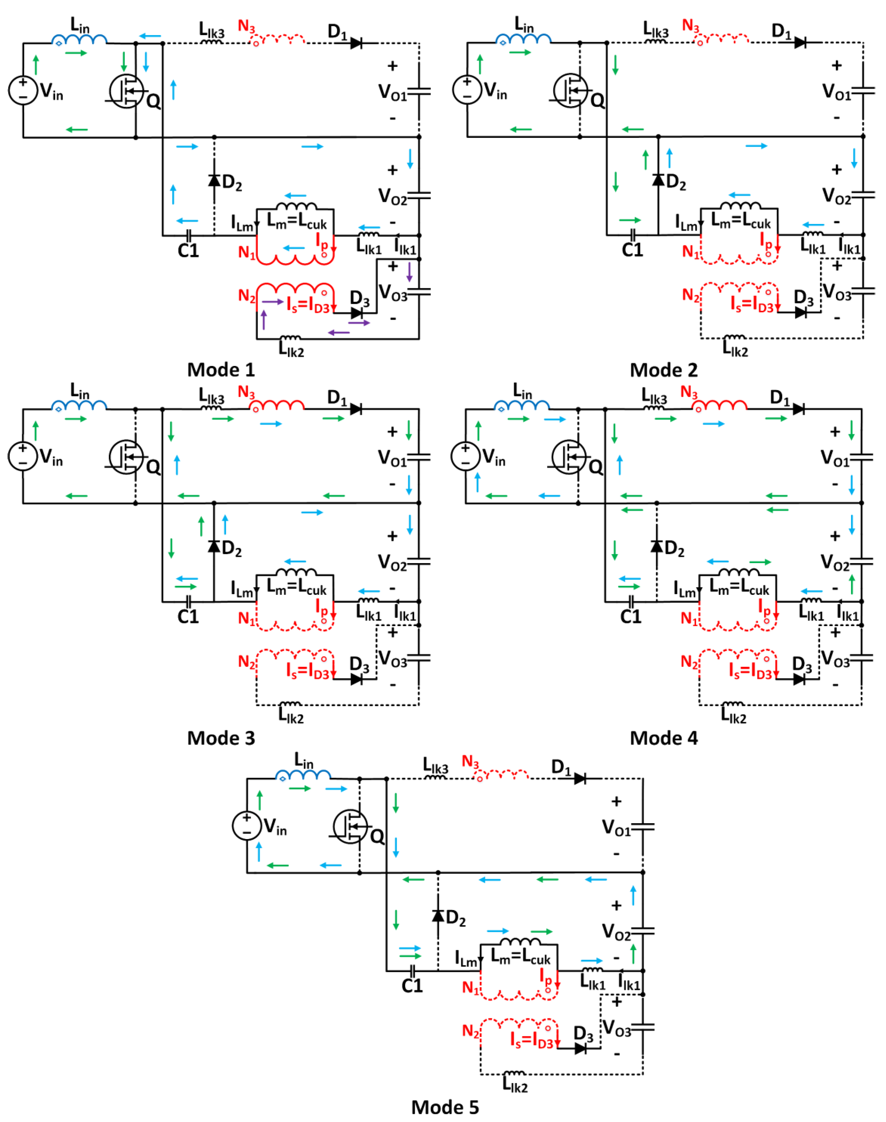
2.1. Operation Basics

The principles of the proposed CBCF converter are explored for one switching cycle in this subsection. In this analysis, all elements of the dc–dc converter are assumed ideal. In this analysis, the magnetizing inductance is considered an output-side Cuk inductance. In addition, all leakage inductances are in series connection with each winding. The winding turn is considered n 1 = N 3 / N i n for the first topology (Figure 1), n 1 = N 3 / N 1 for the second topology (Figure 2), and n 2 = N 2 / N 1 for both topologies. It is proven how to achieve a balanced dc-link voltage and reduced MOSFET voltage stress by the winding turn of the coupled inductors.
In general, the proposed method comprises five modes. The significant waveforms and the current direction of the proposed CBCF for each mode are illustrated in Figure 3 and Figure 4, respectively.
Mode 1 ( t 0 t 1 ): This mode starts with the ZCS turn-on of MOSFET owing to DCM operation and series connection to the output-side Cuk inductor. Both input inductance and output Cuk inductance are linearly charged during this mode.
The voltage of both inductors is the same where the input voltage charges the input inductance while the output Cuk inductance and dc-link capacitor are charged by the Cuk capacitor.
The MOSFET current is the summation of the Cuk inductance current and input current:
I s w = I i n + I l m
where
I i n = I L i n 0 + V i n L i n t
I L m = I L m 0 + V L m L m t = I L i n 0 + V L m L m t
As seen in Equation (3), the initial magnetizing current equals the input current since the primary current ( I P ) is zero at the beginning of this mode. During this mode, however, it is non-zero due to the conduction of D 3 and D 1 .
Moreover, the forward diode ( D 3 ) turns on to charge the third output dc-link capacitor ( C O 3 ).
Mode 2 ( t 1 t 2 ): At the beginning of the second mode, MOSFET is turned off, and the input and magnetizing inductance currents transfer to the Cuk diode ( D 2 ). The voltage of input and magnetizing inductances is reversed, and the voltage of boost and Cuk diodes reduces to zero.
Mode 3 ( t 2 t 3 ): The Cuk diode current transfers to the boost diode, and the boost diode ( D 1 ) experiences a ZCS turn-on. The Cuk diode current becomes zero at the end of the third mode. The first and second dc-link capacitors are charged through the PV voltage, input inductance, and magnetizing inductance, and the magnetizing and input inductance currents reduce linearly.
Mode 4 ( t 3 t 4 ): At the end of the fourth mode, boost and Cuk diodes turn off under ZCS and ZVZCS conditions, respectively. These diodes do not conduct anymore during this switching cycle; therefore, the reverse recovery current loss will be zero.
Mode 5 ( t 4 t 0 ): The voltage of input and magnetizing inductance reduces to zero as a result of DCM operation; hence, their currents remain constant, and the switch voltage reduces to the terminal PV voltage. The fixed input current passes through the Cuk capacitor and magnetizing inductance until the end of the fifth mode. The Cuk capacitor is charged through the input and second dc-link capacitor during this mode.

2.2. Voltage Gain

As previously mentioned, the proposed CBCF is an integration of Cuk, boost, and forward converters with common input for boost and Cuk converters and series output of all three converters. The voltage gain of each converter is extracted based on the voltage per second law in the inductors. In this regard, the voltage of both inductors is a key factor in achieving the voltage gain. According to the first mode in Figure 4, during t = D T , MOSFET is ON:
V L i n = V i n = V m p                                                             t = D T
V L m = V C 1 V o 2                                                               t = D T
The input voltage ( V m p ) is attained by the MPPT strategy from the PV panel. Based on Mode 3 in Figure 4, when the switch is OFF ( t = D ´ T ):
V L i n = V i n V o 1 1 + n 1                                                               t = D ´ T
V L m = V o 2                                                               t = D ´ T
V C 1 = V N 3 + V O 1                                                         t = D ´ T
Because of a low output-side Cuk inductance, CBCF operates in DCM, and the voltage of inductors is zero for the time interval t = T D T D ´ T :
V L i n = V L m = 0
Based on the voltage per second law of the input inductor, the boost voltage gain will be as follows:
V O 1 V i n = D ´ + ( 1 + n 1 ) D D ´ = ( 1 + n 1 ) D D ´ + 1
Similarly for the output Cuk inductor the result is as follows:
V O 2 V C 1 = D D + D ´
To achieve the Cuk voltage gain, the relation between the Cuk capacitor and input voltage can be derived by Equation (8):
V C 1 V i n = D + D ´ D ´
By substituting Equation (12) into Equation (11), the Cuk voltage gain is achieved:
V O 2 V i n = D D ´
As expected, these voltage gains are different; by applying a forward converter with an appropriate winding turn, however, a balanced dc-link voltage can be achieved. In this context, the winding turn n 1 should be first designed to attain the MOSFET low-voltage stress.
As evident, the switch voltage is as follows:
V s w = V C 1 = V N 3 + V O 1                                 t = D ´ T
Since V N 3 is negative when the MOSFET is OFF, we can decrease the MOSFET voltage stress by applying an appropriate winding turn. For example, the first output dc-link voltage for grid-tied application should be 311 V. By considering n 1 = 1 , V N 3 = V L i n = 133 V , the switch voltage will be about 178 V during t = D ´ T , and after this period, the switch voltage reduces to the input voltage. As explored, by selecting an appropriate low-voltage MOSFET, a more efficient converter is attained.
After setting the winding turn of the first coupled inductor, both converters should be compared in terms of voltage gain. According to Equation (10) and n 1 = 1 ,
V O 1 V i n = 311 45.4 = 7 = 1 + 2 D D ´           D D ´ = 3
According to Equations (10) and (13),
V O 1 V O 2 = 1 + 2 D D ´ D D ´ V i n = 1 + D D ´ V i n = 4 V i n
As the discrepancy between the boost and Cuk dc-link voltages is four times the input voltage, by selecting n 2 = N 2 / N 1 = 4 , the forward output dc-link capacitor ( V O 3 ) equals 4 V i n and can compensate for the voltage difference. It must be mentioned that the output Cuk inductance voltage is equal to the terminal PV voltage when MOSFET is ON.

3. Control of the Proposed Converter

3.1. DC–DC Stage

Control of MOSFET generally depends on the application. The proposed converter can be utilized for vast renewable energy storage systems. In this section, however, the PV application is explained. The appropriate voltage and current of a PV panel depends on some parameters like ambient temperature, solar radiation, and shadow effect. The MPPT is realized by techniques like perturb and observe (P & O) procedure. The attained current is the reference current. By comparing the input-side current with the reference current and passing the error of the current through the PI controller the duty cycle is achieved. By the pulse-width modulation (PWM) technique, an appropriate pulse is generated for the main switch. The switching frequency can be adjusted by the PWM method.

3.2. Grid-Side Stage

The grid-side control is also analyzed in this section. In general, the proposed converter can be connected by a half-bridge and a line reactor to the network. The inverter is controlled by grid current. In this context, the dc-link voltage must be passed through a low pass filter (LPF) to remove low-frequency oscillation in the dc-link voltage due to AC load in the output. By comparing this value with the reference voltage and passing through a PI controller, the magnitude of the command network current is achieved. Obviously, the network current is an alternating current. To inject only active power, the per-unit grid voltage is multiplied by the magnitude of the command network current to attain a sinusoidal command network current with a unity power factor. The half-bridge inverter can be controlled by hysteresis control. In this regard, the measured network current is compared to the command current, and then, the current error is passed through the hysteresis band. Figure 5 depicts the control procedure of both the input and network sides for PV applications.
As mentioned, the dc-link voltage has low-frequency oscillation. The amplitude of this oscillation depends on the injected power into the network. As microinverters are low-power, the oscillation of the dc-link voltage is lower than 10% of the total dc-link voltage. Hence, the voltage reference about V o * = 330 340 V is sufficient for this reference value. When V o * is compared with the minimum voltage level, it will be also valid for the higher one. Thus, a low THD current without any distortion is achieved.

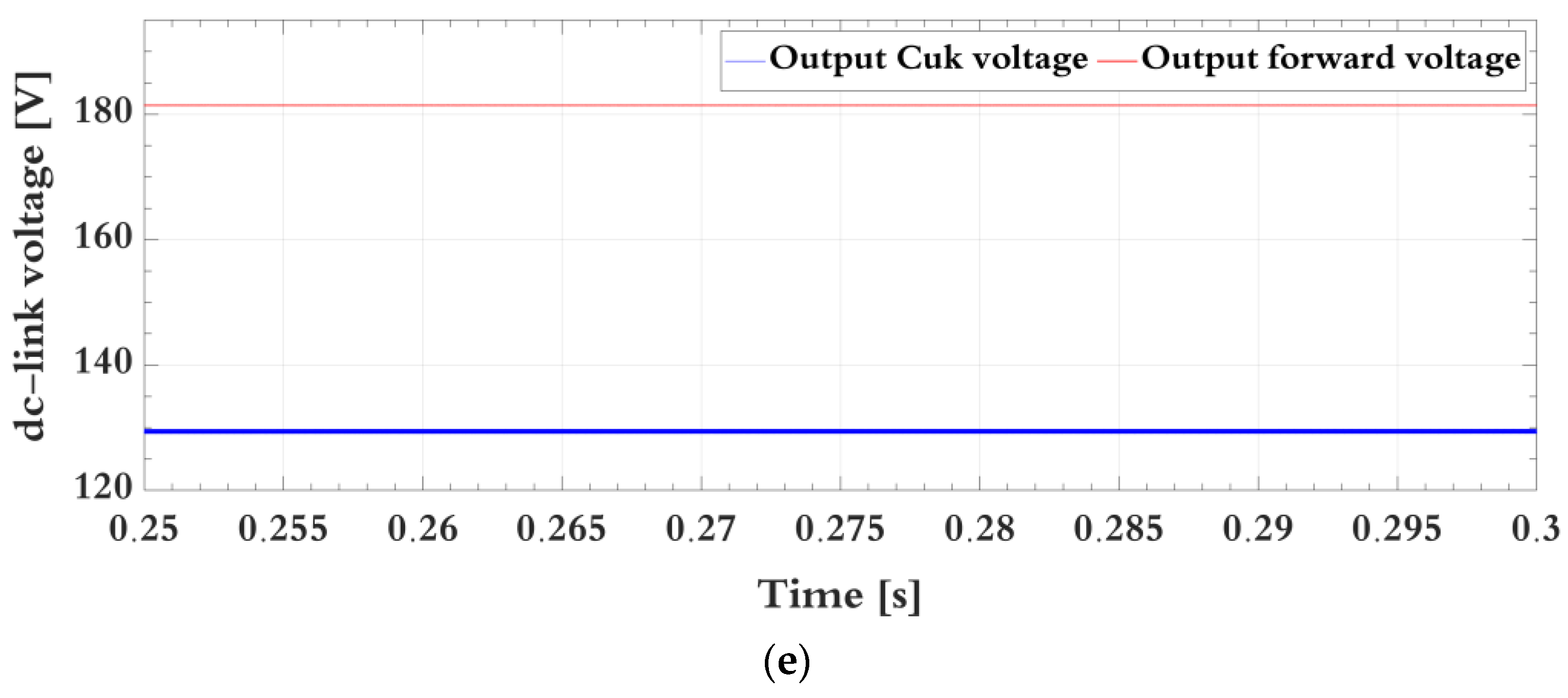
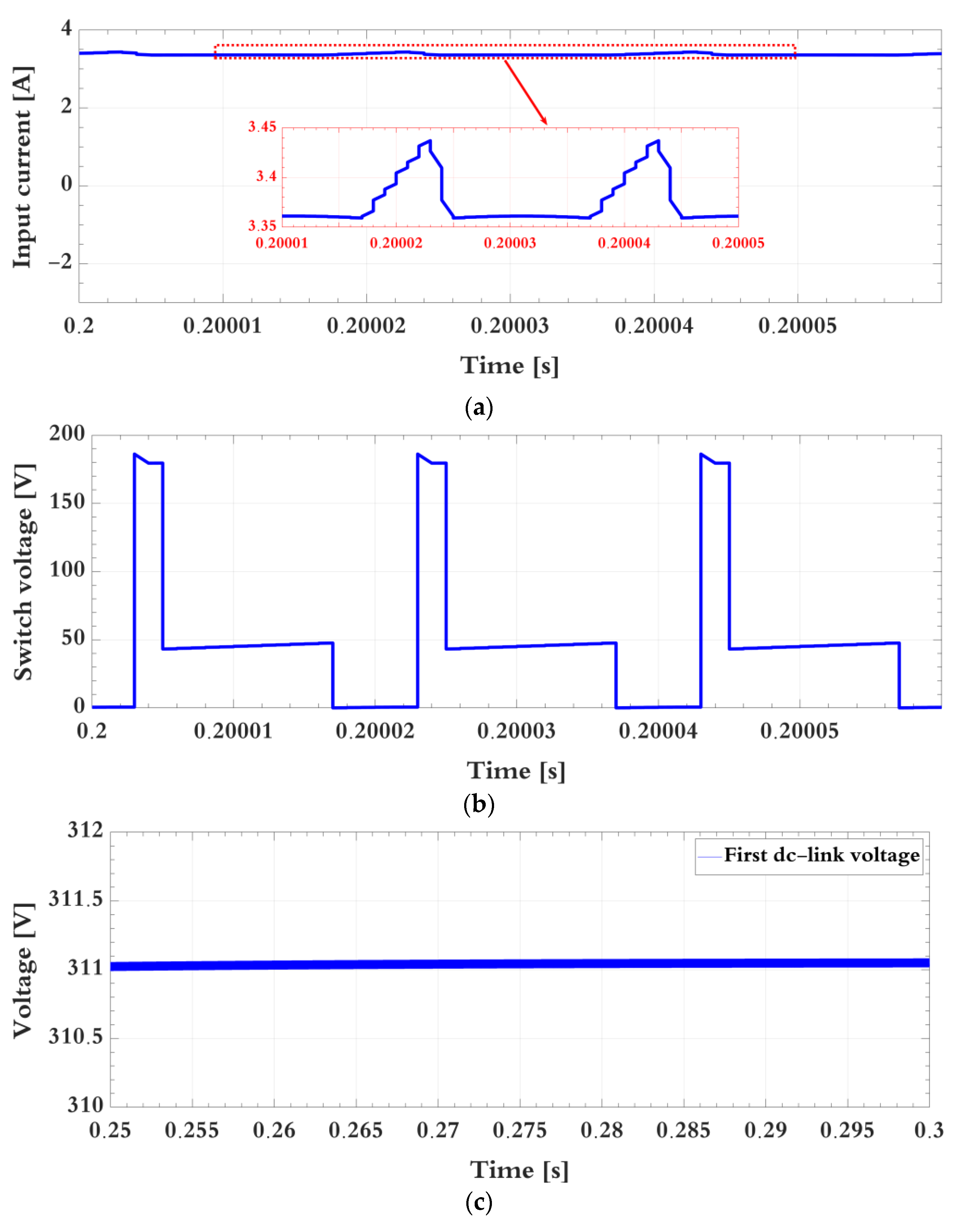
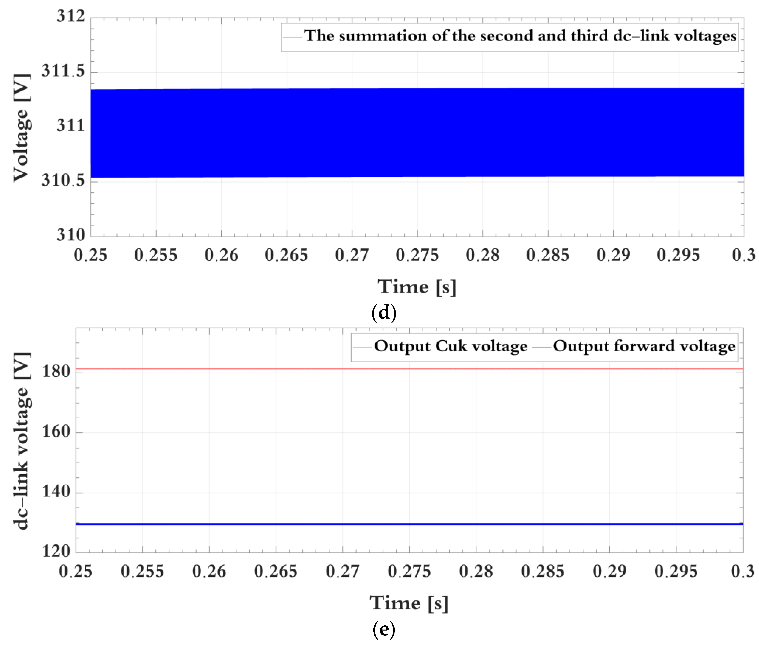
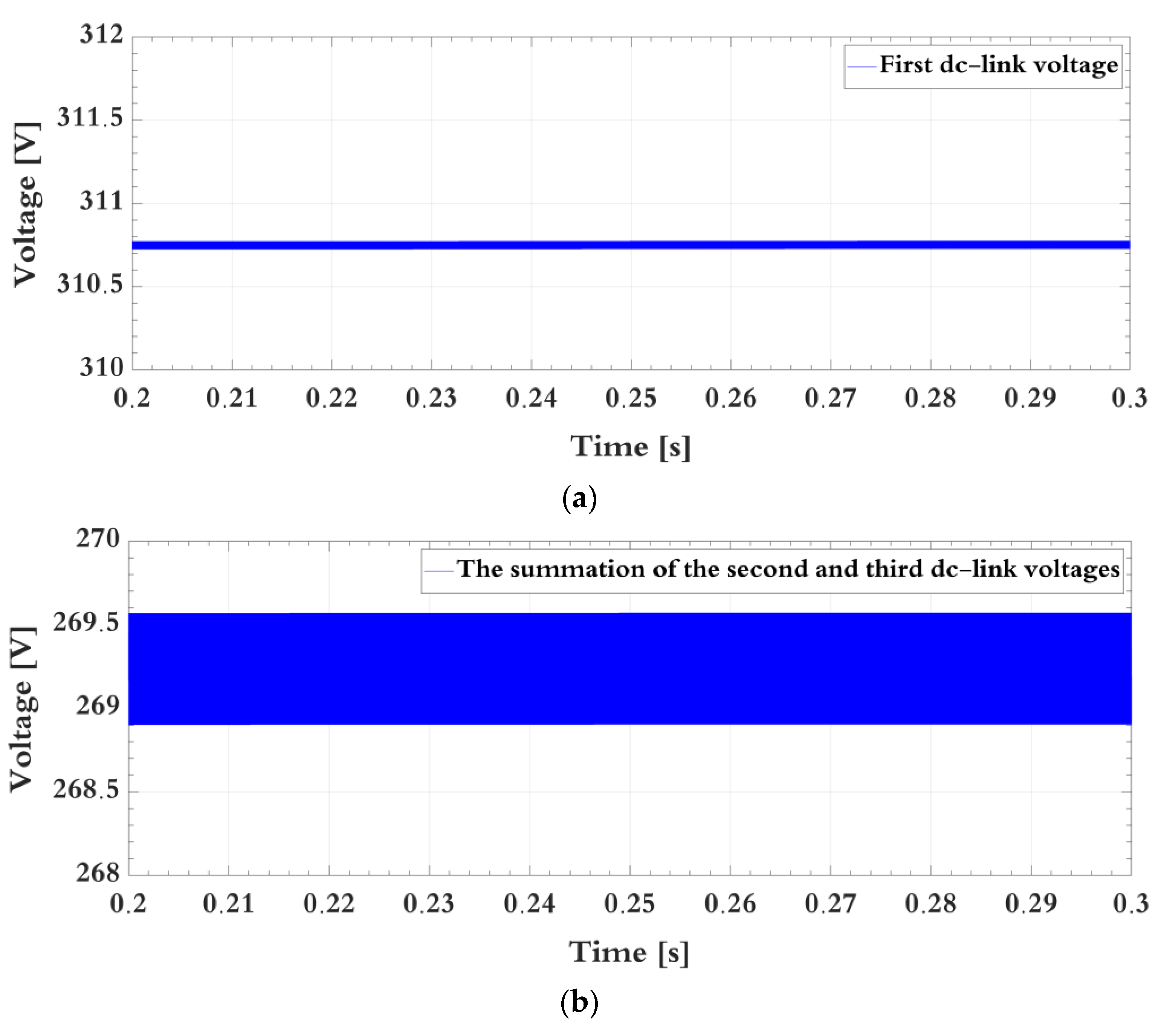
4. Simulation Outcomes

The simulation analyses of the proposed CBCF, which are illustrated in Figure 1 and Figure 2, are provided and compared. The elements used for experimental and simulation analyses are tabulated in Table 1. As already mentioned, the coupled inductor, which has a series connection with the boost diode, is applied to decrease the switch voltage stress. This inductor can be coupled with the input-side inductor or output Cuk inductor since the voltage of both inductors is the same. Figure 6 demonstrates the simulation analyses of the inductor coupled with the input inductor while Figure 7 shows the simulation results of the inductor coupled with the output Cuk inductor at the rate power of 150 W. As indicated, the input current is almost free ripple when the inductor is coupled with the output Cuk inductor (Figure 6a and Figure 7a). Free ripple input current is necessary for most renewable energy system applications. The output Cuk inductor in the proposed converter provides this ability to be coupled with the inductor, which is in series with the boost diode. As seen in Figure 6b and Figure 7b, both techniques have an acceptable performance to reduce the switch voltage stress. In addition, the balanced output dc-link voltages are investigated in Figure 6c,d and Figure 7c,d. Furthermore, the effect of input voltage variations on the dc-link voltage is explored in Figure 8. The stress voltage and current of all semiconductor elements are tabulated in Table 2.
The effect of input voltage variation is analyzed for the topology shown in Figure 2. In this regard, 30% input voltage reduction is considered ( V i n = 32 V ). According to Equation (15), the ratio D D ´ = 4.36 , and therefore, the winding turn ratio of the forward converter should be n 2 = 5.36 to achieve a balanced dc-link voltage; however, as we designed this ratio at n 2 = 4 , the voltage difference between the two dc-link voltages is 32 × 1.36 = 44 V. As seen, the voltage difference is lower than 10% of the total dc-link voltage (622 V). Also, for grid-tied applications, the reference dc-link voltage must be considered at a higher value since the dc-link voltage has low-frequency oscillations equal to twice the grid frequency. Thus, this difference is negligible.

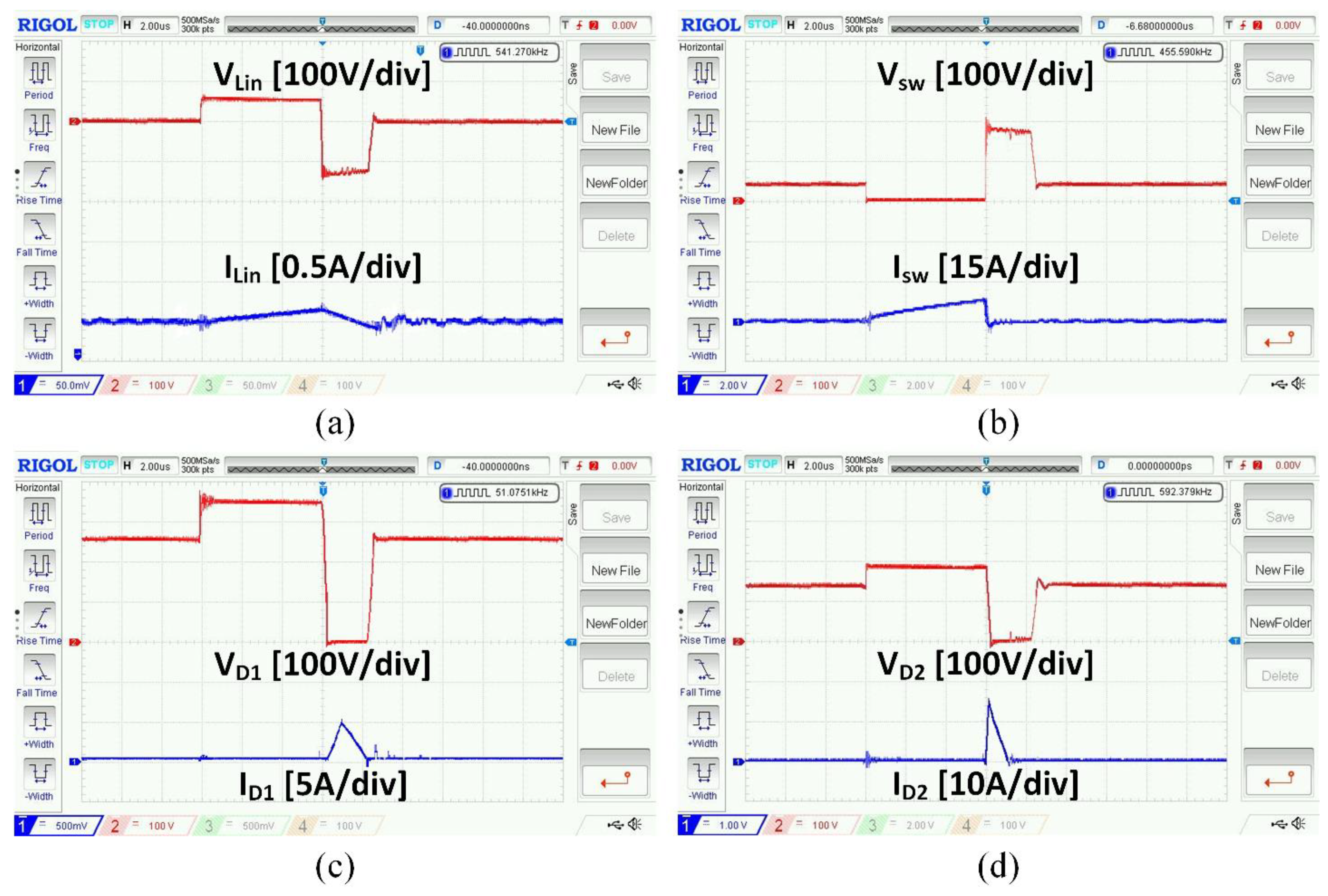
5. Experimental Verifications

The practical performance of the proposed CBCF depicted in Figure 2 is investigated in this section. Figure 9 shows the 150 W prototype of the proposed CBCF.

5.1. Performance of the Proposed Converter

The experimental results of the main elements at the rate power of 150 W are illustrated in Figure 10. The results substantiate the theoretical analyses provided in Section 2.
Figure 10a indicates the voltage (red) and current (blue) of the input inductance where the voltage per second law is valid. The duty cycle is about 30%. The current is almost ripple free which proves the proposed CBCF is operative for almost all renewable energy systems.
Moreover, Figure 10b proves MOSFET voltage stress is reduced by 180 V, which results in utilizing a low-resistance MOSFET and achieving a more efficient converter. Besides, MOSFET is turned on under ZCS and low-voltage conditions since the proposed converter operates at DCM. Removing the reverse recovery current loss is another advantage of the DCM operation of the proposed CBCF due to the ZVS turn-off of the boost diode and ZVZCS turn-off of the Cuk diode before MOSFET being turned on.
The voltage (red) and current (blue) of the boost and Cuk diodes are illustrated in Figure 10c,d, respectively. As seen, the Cuk diode first conducts as soon as MOSFET is turned off. Then, the boost diode passes the current. Finally, both diodes turn off under soft-switching conditions.
Figure 11a illustrates the balanced dc-link voltage. The blue curve corresponds to the output boost converter and the red curve shows the summation of Cuk and forward converters. In addition, the voltage of Cuk and forward is depicted in Figure 11b, which substantiates the theoretical analyses mentioned in Section 2.2.

5.2. Efficiency Analysis

The proposed converter is compared with other studies in terms of MOSFET voltage stress, input current ripple, number of elements, and efficiency (Table 3). As seen, the voltage difference between the output and input of the proposed converter is higher than other topologies. Also, the efficiency of the proposed converter is 93.07% while the MOSFET is not fully soft-switched because of hard turn-off conditions. It must be mentioned that the switching loss is the highest one in the HSU converters.
In addition, the proposed converter has only one MOSFET, which makes the control algorithm easier.

6. Conclusions

In this research, a new integrated boost-Cuk-forward HSU is proposed for renewable energy storage systems. In this topology, a common inductor and MOSFET are used on the PV side for boost and Cuk converters while the output capacitor of the boost is in series with the Cuk capacitor to lift the level of voltage effectively. As proved, the output voltage of these converters is not identical due to the different voltage gain of these converters. As the output-side Cuk inductor has a voltage similar to the input inductor, a forward-based inductor is coupled with the Cuk inductor to charge the output forward capacitor, balance the dc-link for extensive input voltage variations, and make the proposed CBCF appropriate for wider applications like grid-connected application. Additionally, as the PV ground is connected in between the dc-link in the proposed CBCF, the grid ground can be simply connected to the PV ground by a half-bridge inverter. Consequently, the PV-side ground leakage current will be removed in this CBCF.
To attain the low-voltage stress of MOSFET, another coupled inductor is applied in series with the boost diode. As illustrated, this coupled inductor provides a ripple-free input current which is another advantage of the proposed topology.
The output-side Cuk inductance is designed to be very small to provide DCM operation for the proposed converter. Hence, MOSFET is turned on under ZCS and low voltage conditions, and Cuk and boost diodes turn off before the main switch is turned on. Therefore, the reverse recovery current loss becomes zero and the converter operates efficiently. The practical performance of CBCF proves the proposed converter will be applicable for various renewable energy storage systems such as PV panels where a highly reliable and efficient converter is of the essence.

Author Contributions

Simulation, writing—original draft preparation, and writing—review and editing by R.H.; conceptualization, and formal analysis by M.A.G.; investigation, validation, and methodology by E.A., funding acquisition by K.-I.J.; supervision and project administration by J.-W.A.; All authors have read and agreed to the published version of the manuscript.

Funding

This study was supported by “Leaders in INdustry-university Cooperation 3.0” Project, supported by the Ministry of Education and National Research Foundation of Korea and Basic Science Research Program through the National Research Foundation of Korea (NRF) funded by the Ministry of Education (2020R1G1A1012756).

Institutional Review Board Statement

Not applicable.

Data Availability Statement

Not applicable.

Conflicts of Interest

There are no conflict of interest among authors.

References

  1. Son, S.; Montes, O.A.; Junyent-Ferré, A.; Kim, M. High Step-Up Resonant DC/DC Converter with Balanced Capacitor Voltage for Distributed Generation Systems. IEEE Trans. Power Electron. 2019, 34, 4375–4387. [Google Scholar] [CrossRef]
  2. Poorali, B.; Jazi, H.M.; Adib, E. Improved High Step-Up Z-Source DC–DC Converter with Single Core and ZVT Operation. IEEE Trans. Power Electron. 2018, 33, 9647–9655. [Google Scholar] [CrossRef]
  3. Hou, S.; Chen, J.; Sun, T.; Bi, X. Multi-input Step-Up Converters Based on the Switched-Diode-Capacitor Voltage Accumulator. IEEE Trans. Power Electron. 2016, 31, 381–393. [Google Scholar] [CrossRef]
  4. Pervez, I.; Antoniadis, C.; Ghazzai, H.; Massoud, Y. A Centralized Multi-String PV System Control with Multi-Dimensional MPPT Control. In Proceedings of the 2022 IEEE Asia Pacific Conference on Circuits and Systems (APCCAS), Shenzhen, China, 11–13 November 2022; pp. 304–308. [Google Scholar]
  5. Yagoub, M.A.; Elserougi, A.A.; Abdelhamid, T.H. Assessment of PV String Optimizer Circuit Versus String and Central Inverters During Partial Shading Conditions. In Proceedings of the 2021 22nd International Middle East Power Systems Conference (MEPCON), Assiut, Egypt, 14–16 December 2021; pp. 14–19. [Google Scholar]
  6. Xiao, H.; Xu, T.; Xiang, L.; Zhang, Z.; Xie, S.; Liu, D. A Variable Phase-Shift Control Scheme for Extended-Duty-Ratio Boost Converter with Automatic Current Sharing in High Step-up High Current Application. IEEE Trans. Ind. Electron. 2021, 68, 6794–6805. [Google Scholar] [CrossRef]
  7. Lei, H.; Hao, R.; You, X.; Li, F. Nonisolated High Step-Up Soft-Switching DC–DC Converter with Interleaving and Dickson Switched-Capacitor Techniques. IEEE J. Emerg. Selec. Top. Power Electron. 2020, 8, 2007–2021. [Google Scholar] [CrossRef]
  8. Hassan, W.; Lu, D.D.-C.; Xiao, W. Single-Switch High Step-Up DC–DC Converter with Low and Steady Switch Voltage Stress. IEEE Trans. Ind. Electron. 2019, 66, 9326–9338. [Google Scholar] [CrossRef]
  9. Abbasi, M.; Lam, J. A Modular SiC-Based Step-Up Converter with Soft-Switching-Assisted Networks and Internally Coupled High-Voltage-Gain Modules for Wind Energy System with a Medium-Voltage DC-Grid. IEEE J. Emerg. Selec. Top. Power Electron. 2019, 7, 798–810. [Google Scholar] [CrossRef]
  10. Li, X.; Zhang, Y.; Liu, J.; Gao, Y.; Cao, M. A Universal ZVT Design for a Family of Multiphase Interleaved High Step-Up Converters with Minimized Voltage Stress and Wide Operating Range. IEEE Trans. Power Electron. 2021, 36, 13779–13791. [Google Scholar] [CrossRef]
  11. Liu, J.; Wang, K.; Zheng, Z.; Li, C.; Li, Y. A Dual-Active-Clamp Quasi-Resonant Isolated Boost Converter for PV Integration to Medium-Voltage DC Grids. IEEE J. Emerg. Selec. Top. Power Electron. 2020, 8, 3444–3456. [Google Scholar] [CrossRef]
  12. Chao, K.-H.; Kuo, Y.-P.; Chen, H.-H. Design and Implementation of a Soft-Switching Converter with High Step-Up Ratio. IEEE Access 2023, 11, 48506–48516. [Google Scholar] [CrossRef]
  13. Jia, P.; Su, Z.; Shao, T.; Mei, Y. An Isolated High Step-Up Converter Based on the Active Secondary-Side Quasi-Resonant Loops. IEEE Trans. Power Electron. 2022, 37, 659–673. [Google Scholar] [CrossRef]
  14. Rajabi, A.; Rajaei, A.; Tehrani, V.M.; Dehghanian, P.; Guerrero, J.M.; Khan, B. A Non-Isolated High Step-Up DC-DC Converter Using Voltage Lift Technique: Analysis, Design, and Implementation. IEEE Access 2022, 10, 6338–6347. [Google Scholar] [CrossRef]
  15. Arshadi, S.A.; Poorali, B.; Adib, E.; Farzanehfard, H. High Step-Up DC–AC Inverter Suitable for AC Module Applications. IEEE Trans. Ind. Electron. 2016, 63, 832–839. [Google Scholar] [CrossRef]
  16. She, J.-M.; Jou, H.-L.; Wu, J.-C. Novel transformerless grid-connected power converter with negative grounding for photovoltaic generation system. IEEE Trans. Power Electron. 2012, 27, 1818–1829. [Google Scholar]
  17. Heidari, R.; Adib, E.; Jeong, K.-I.; Ahn, J.-W. Soft-switched Boost-cuk-type High Step-up Converter for Grid-tied with Half-bridge Inverter. IEEE J. Emerg. Selec. Top. Power Electron. 2022, 11, 786–795. [Google Scholar] [CrossRef]
  18. Nathan, K.; Ghosh, S.; Siwakoti, Y.; Long, T. A New DC-DC Converter for Photovoltaic Systems: Coupled-Inductors Combined Cuk-SEPIC Converter. IEEE Trans. Energy Conv. 2019, 34, 191–201. [Google Scholar] [CrossRef]
  19. Ferrera, M.B.; Litrán, S.P.; Durán Aranda, E.; Andújar Márquez, J.M. A Converter for Bipolar DC Link Based on SEPIC-Cuk Combination. IEEE Trans. Power Electron. 2015, 30, 6483–6487. [Google Scholar] [CrossRef]
  20. Tamyurek, B.; Kirimer, B. An Interleaved High-Power Flyback Inverter for Photovoltaic Applications. IEEE Trans. Power Electron. 2015, 30, 3228–3241. [Google Scholar] [CrossRef]
  21. Zhang, F.; Xie, Y.; Hu, Y.; Chen, G.; Wang, X. A Hybrid Boost–Flyback/Flyback Microinverter for Photovoltaic Applications. IEEE Trans. Ind. Electron. 2020, 67, 308–318. [Google Scholar] [CrossRef]
  22. Shirmohammadi, S.; Suh, Y. Multiwinding Flyback Clamp Snubber for 10 kV IGCT with Reduced Voltage Stress on Clamp Recovery Diodes. IEEE Trans. Ind. Appl. 2020, 56, 2729–2740. [Google Scholar] [CrossRef]
  23. Sathyan, S.; Suryawanshi, H.M.; Ballal, M.S.; Shitole, A.B. Soft-Switching DC–DC Converter for Distributed Energy Sources with High Step-Up Voltage Capability. IEEE Trans. Ind. Electron. 2015, 62, 7039–7050. [Google Scholar] [CrossRef]
  24. Gao, S.; Sang, X.; Wang, Y.; Liu, Y.; Guan, Y.; Xu, D. A DCM High-Frequency High-Step-Up SEPIC-Based Converter with Extended ZVS Range. IEEE J. Emerg. Selec. Top. Power Electron. 2022, 10, 7915–7924. [Google Scholar] [CrossRef]
  25. Kim, J.-K.; Moon, G.-W. Derivation, Analysis, and Comparison of Nonisolated Single-Switch High Step-up Converters with Low Voltage Stress. IEEE Trans. Power Electron. 2015, 30, 1336–1344. [Google Scholar] [CrossRef]
  26. Seshagiri, R.V.; Kumaravel, S. Ultra-Voltage Gain Bidirectional DC–DC Converter With Reduced Switch Voltage Stress and Improved Efficiency. IEEE Trans. Circuits Syst. II: Express Briefs 2022, 69, 4468–4472. [Google Scholar]
  27. Yang, P.; Xu, J.; Zhou, G.; Zhang, S. A new quadratic boost converter with high voltage step-up ratio and reduced voltage stress. In Proceedings of the 7th International Power Electronics and Motion Control Conference, Harbin, China, 2–5 June 2012; pp. 1164–1168. [Google Scholar]
  28. Zeng, T.; Wu, Z.; He, L. An Interleaved Soft Switching High Step-Up Converter with Low Input Current Ripple and High Efficiency. IEEE Access 2019, 7, 93580–93593. [Google Scholar] [CrossRef]
  29. Zheng, Y.; Brown, B.; Xie, W.; Li, S.; Smedley, K. High Step-Up DC–DC Converter with Zero Voltage Switching and Low Input Current Ripple. IEEE Trans. Power Electron. 2020, 35, 9416–9429. [Google Scholar] [CrossRef]
  30. Zaoskoufis, K.; Tatakis, E.C. Isolated ZVS-ZCS DC–DC High Step-Up Converter with Low-Ripple Input Current. IEEE J. Emerg. Selec. Top. Ind. Electron. 2021, 2, 464–480. [Google Scholar] [CrossRef]
Figure 1. Proposed converter where the inductor ( L 3 ) is coupled with the input-side inductor.
Energies 16 06391 g001
Figure 2. Proposed converter where the inductor ( L 3 ) is coupled with the output-side Cuk inductor.
Energies 16 06391 g002
Figure 3. Key waveforms of the main elements.
Energies 16 06391 g003
Figure 4. Five operating modes of the proposed method.
Energies 16 06391 g004
Figure 5. The control of the input-side dc–dc and grid-side stages for PV applications.
Energies 16 06391 g005
Figure 6. The simulations of the proposed CBCF topology depicted in Figure 1 at the rated power of 150 W: (a) Input-side current, (b) switch voltage, (c) first dc-link voltage ( V O 1 ), (d) the summation of Cuk and forward dc-link ( V O 2 + V O 3 ), and (e) Cuk and forward dc-link voltages.
Energies 16 06391 g006aEnergies 16 06391 g006b
Figure 7. The simulations of the proposed CBCF topology depicted in Figure 2 at the rated power of 150 W: (a) input-side current, (b) switch voltage, (c) first dc-link voltage ( V O 1 ), (d) the summation of Cuk and forward dc-link ( V O 2 + V O 3 ), and (e) Cuk and forward dc-link voltages.
Energies 16 06391 g007aEnergies 16 06391 g007b
Figure 8. The simulations of the proposed CBCF topology depicted in Figure 2 at 70% of the rated input voltage: (a) first dc-link voltage ( V O 1 ), (b) the summation of Cuk and forward dc-link ( V O 2 + V O 3 ), and (c) Cuk and forward dc-link voltages.
Energies 16 06391 g008aEnergies 16 06391 g008b
Figure 9. Experimental prototype of the proposed CBCF.
Energies 16 06391 g009
Figure 10. Experimental outcomes at the rated power of 150 W: (a) voltage (red) and current (blue) of the input inductor, (b) voltage (red) and current (blue) of MOSFET, (c) voltage (red) and current (blue) of the boost diode, and (d) voltage (red) and current (blue) of the Cuk diode.
Energies 16 06391 g010
Figure 11. Experimental outcomes of balanced dc-link voltage at the rated power of 150 W: (a) output boost converter (blue) and the summation of the output Cuk and forward converters (red), and (b) output Cuk converter (blue) and output forward converter (red).
Energies 16 06391 g011
Table 1. Applied elements in the proposed CBCF.
SignsParametersValue
PVSolar moduleNA-E130G
V m p Voltage at MPP45.4 v
I m p Current at MPP3.3 A
V g Grid voltage220 Vrms
L g Grid inductance4 mH
f s w Switching frequency50 KHz
L i n Input inductance800 uH
L m Cuk inductance17 uH
L l k 1 Cuk leakage inductance1 uH
L l k 2 Forward leakage inductance1 uH
L l k 3 Third leakage inductance2 uH
kCoupling coefficient0.96
n 1 First turn ratio1
n 2 Second turn ratio4
C o 1 ,   C o 2 ,   a n d   C o 3 Output capacitor66 uF
QMain switchIRFP4668
D 1 Boost diodeMUR860
D 2 Cuk diodeMUR860
D 3 Forward diodeUF5408
C 1 Cuk capacitance5.6 uF
L g Grid inductance3 mH
S 1 & S 2 H-bridge switchFGL40n120
Table 2. Stress voltage and current of all elements.
ElementsPeak VoltagePeak Current
Switch Q 0.5 ( V O 1 + V i n ) I L c u k , m a x + 1.1 I L i n
Diode   D 1 V O 2 + V i n 1.1 I L i n
Diode   D 2 V O 1 + V i n I L c u k , m a x + 1.1 I L i n
Diode   D 3 2 ( V O 1 V i n ) I D 3 m a x C O 3
Table 3. Comparison of the proposed converter with previous converters.
Ref.No. of Passive ElementsNo. of SemiconductorsSwitching ConditionInput Current RippleMOSFET
Stress Voltage
Efficiency
[23]
12 V/120 V
3 inductors
5 capacitors
2 switches
2 diodes
SoftHighHigh91.8%
[24]
24 V/250 V
2 inductors
3 capacitors
1 switch
3 diodes
HardHighLow89%
[28]
40 V/400 V
3 inductors
4 capacitors
2 switches
2 diodes
SoftLowHigh94.8%
[30]
30 V/200 V
5 inductors
5 capacitors
1 switch
4 diodes
SoftLowLow94.2%
Proposed
45 V/622 V
4 inductors
4 capacitors
1 switch
3 diodes
HardLowLow93.07%
Disclaimer/Publisher’s Note: The statements, opinions and data contained in all publications are solely those of the individual author(s) and contributor(s) and not of MDPI and/or the editor(s). MDPI and/or the editor(s) disclaim responsibility for any injury to people or property resulting from any ideas, methods, instructions or products referred to in the content.

