
Non-Isolated Current-Fed Series Resonant Converter with Hybrid Control Algorithms for DC Microgrid


Abstract
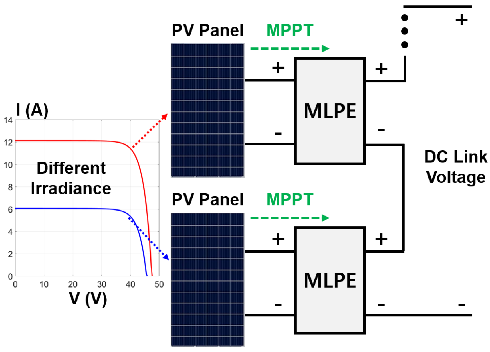
:1. Introduction
2. Analysis of Proposed Converter
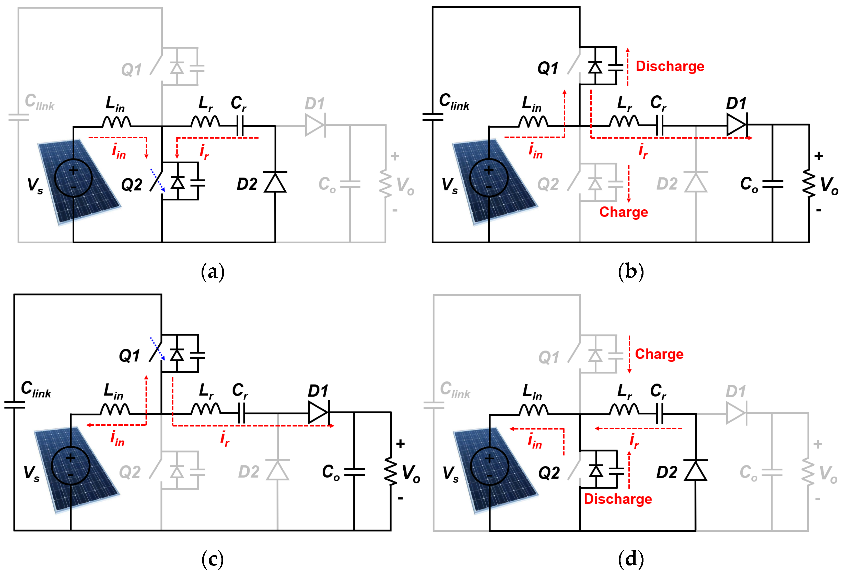
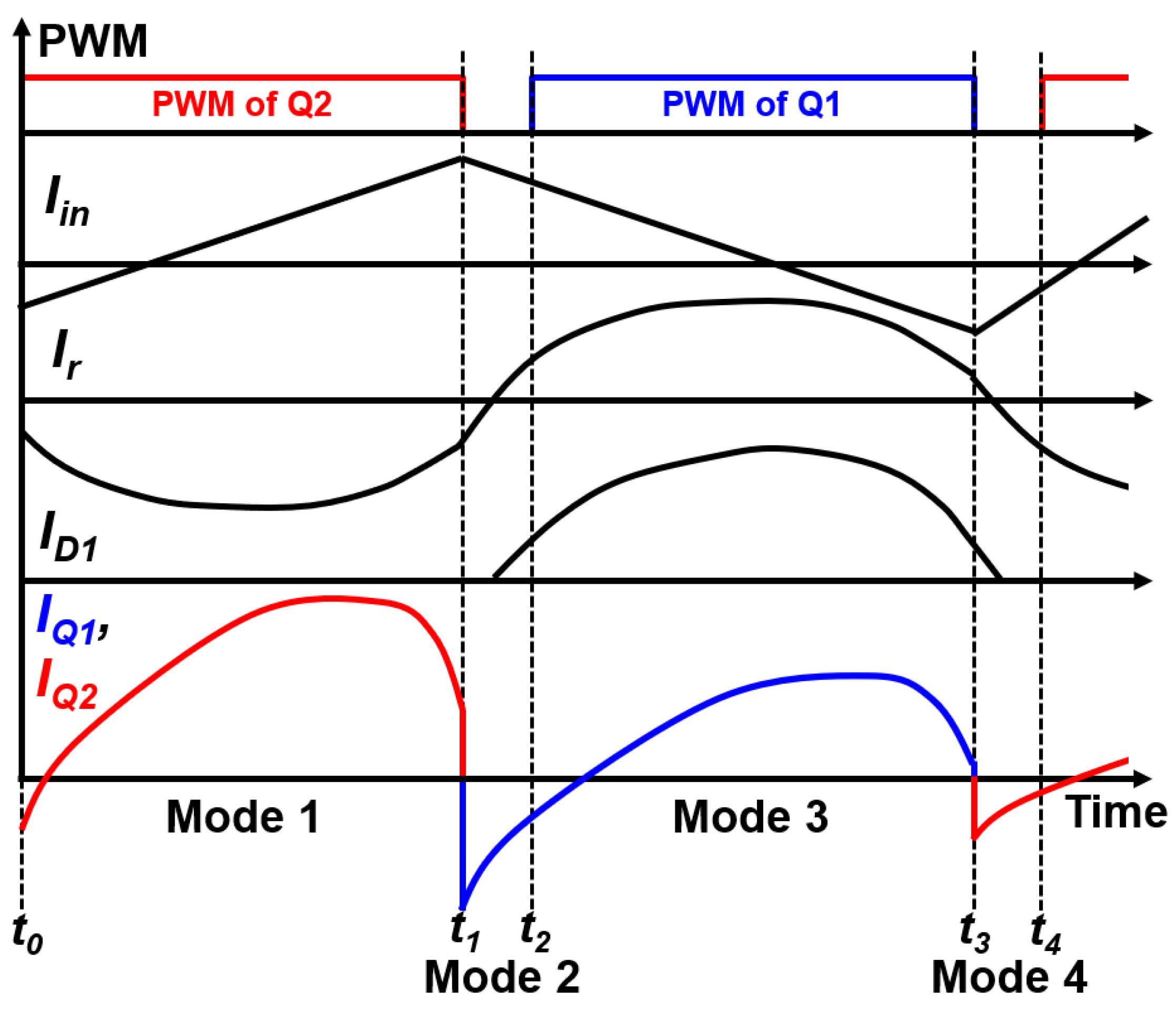
2.1. Mode 1 (t0 − t1)
2.2. Mode 2 (t1 − t2)
2.3. Mode 3 (t2 − t3)
2.4. Mode 4 (t3 − t4)
3. Design Methodology
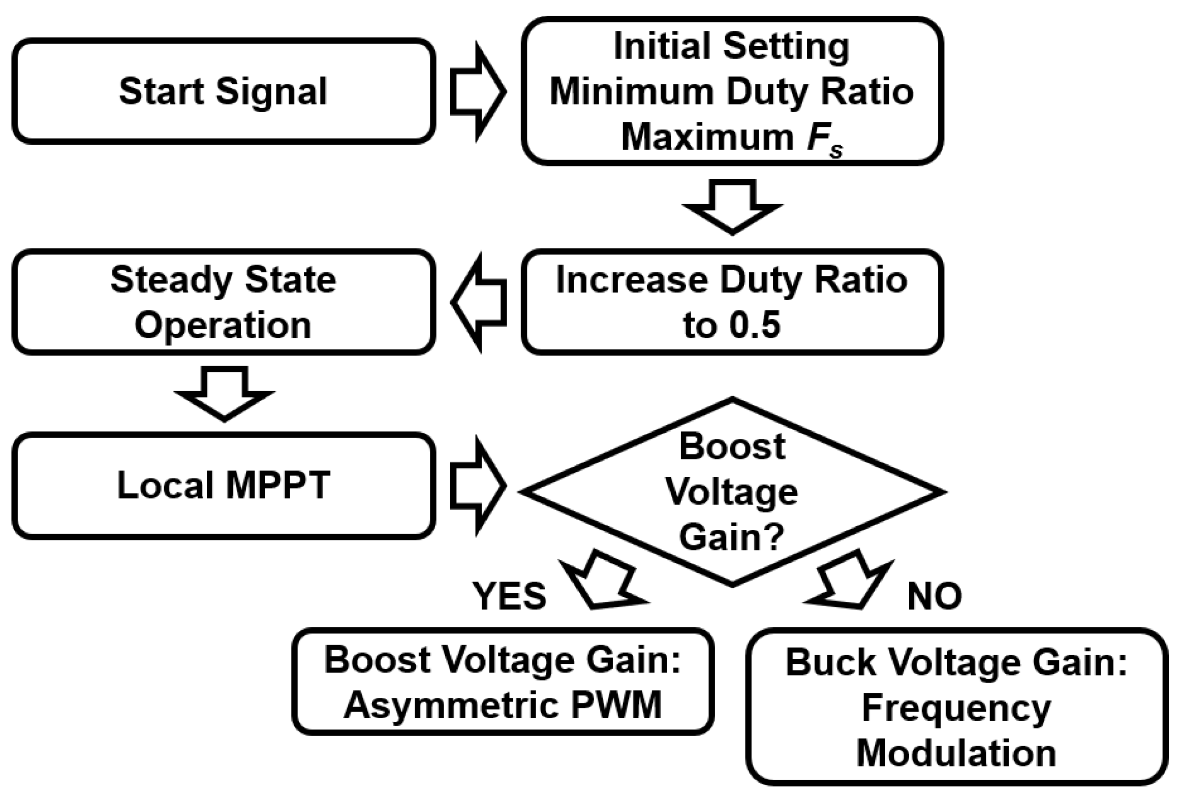
3.1. Control Algorithm
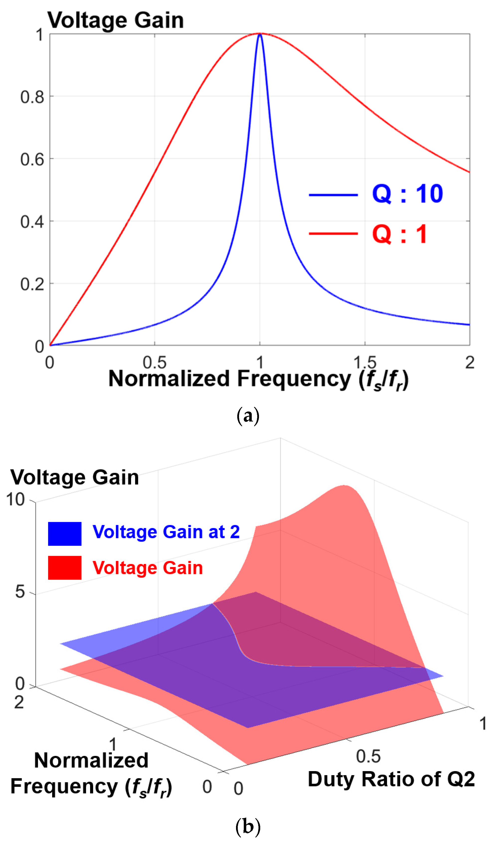
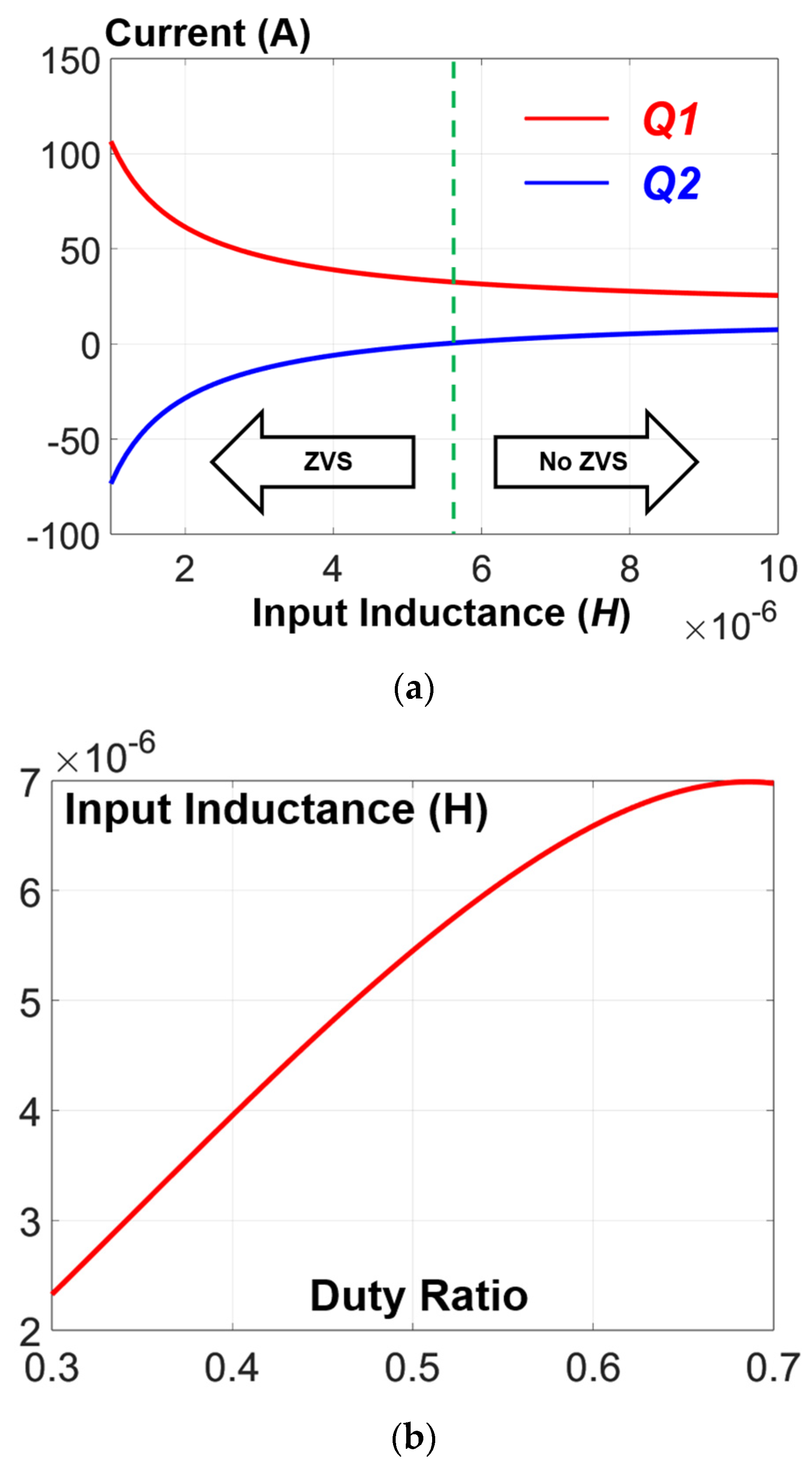
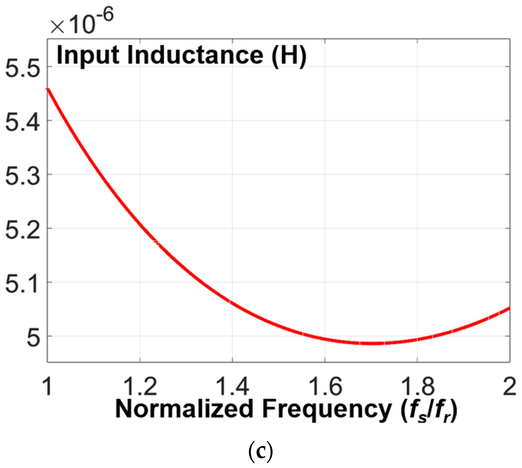
3.2. Soft Switching Capability
3.3. Analysis of RMS Current
3.4. Design Example
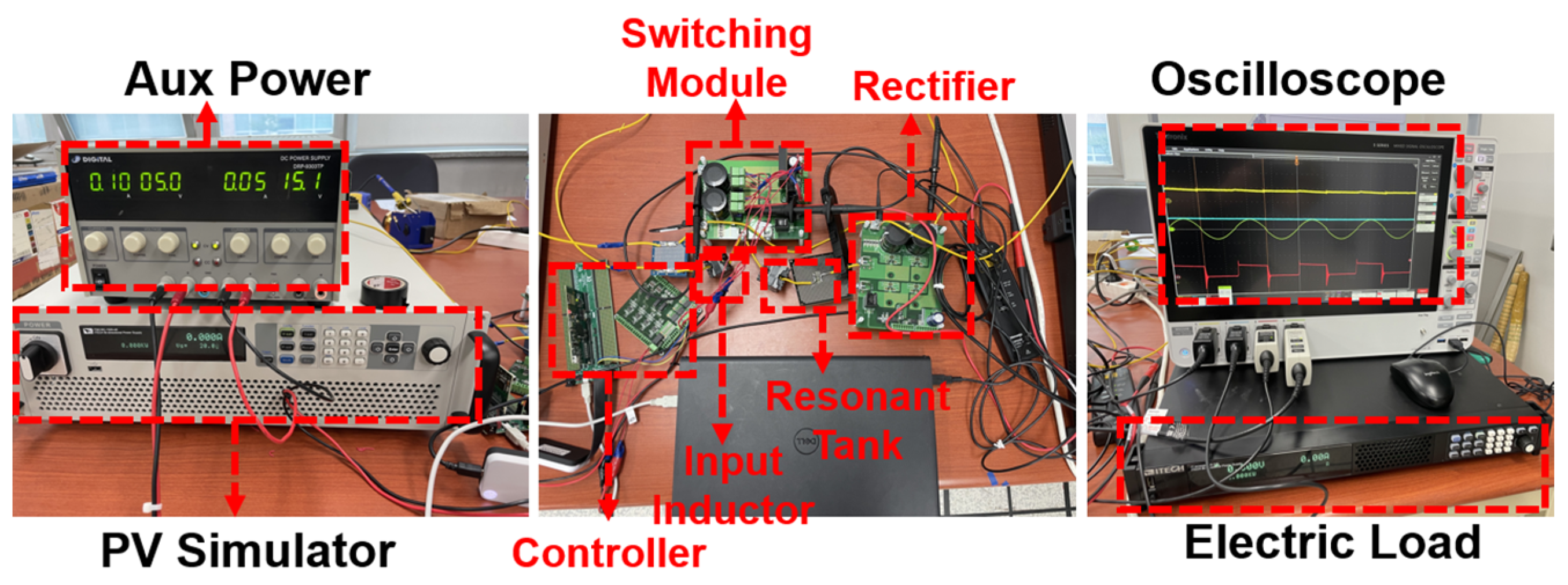
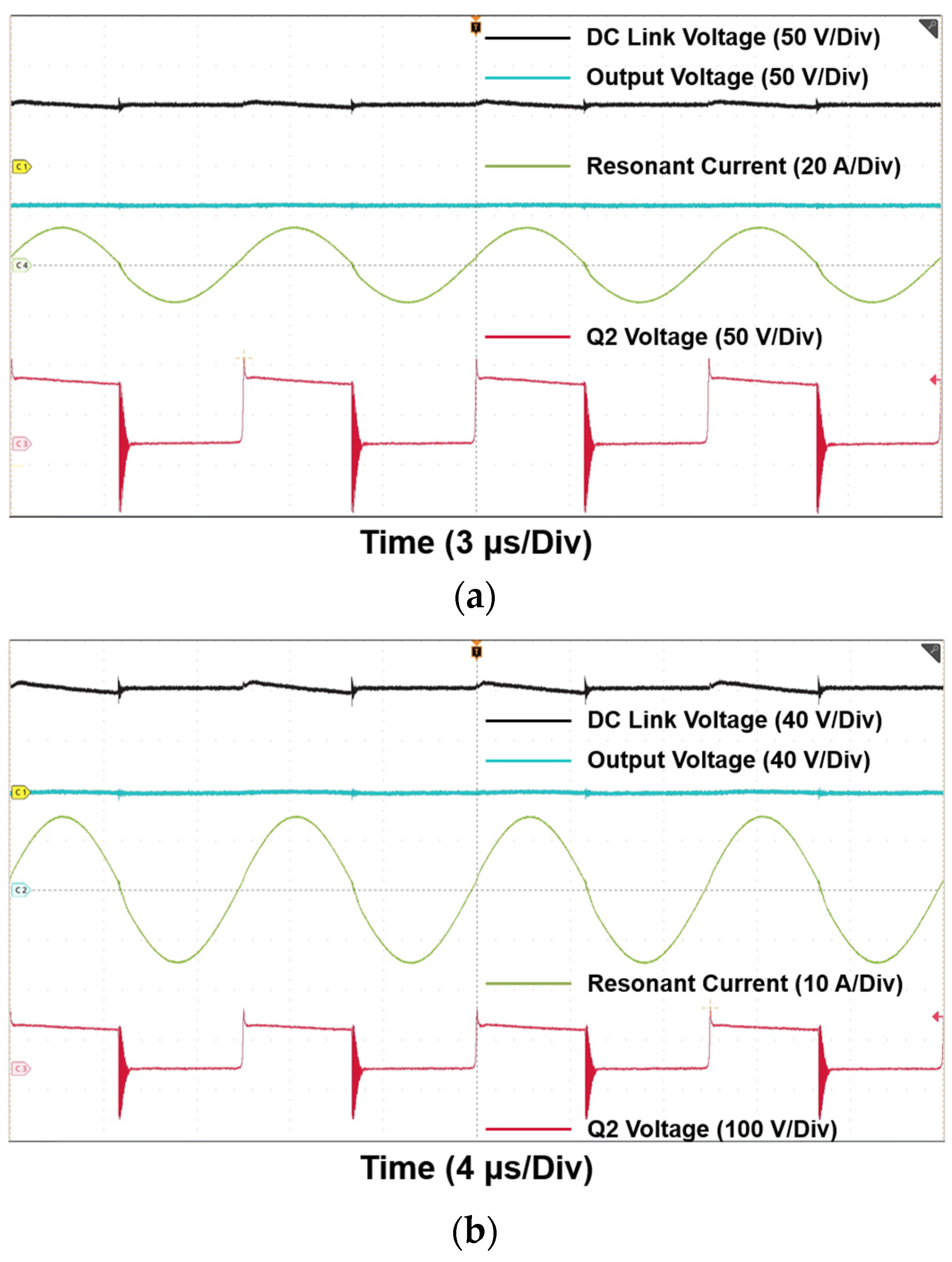
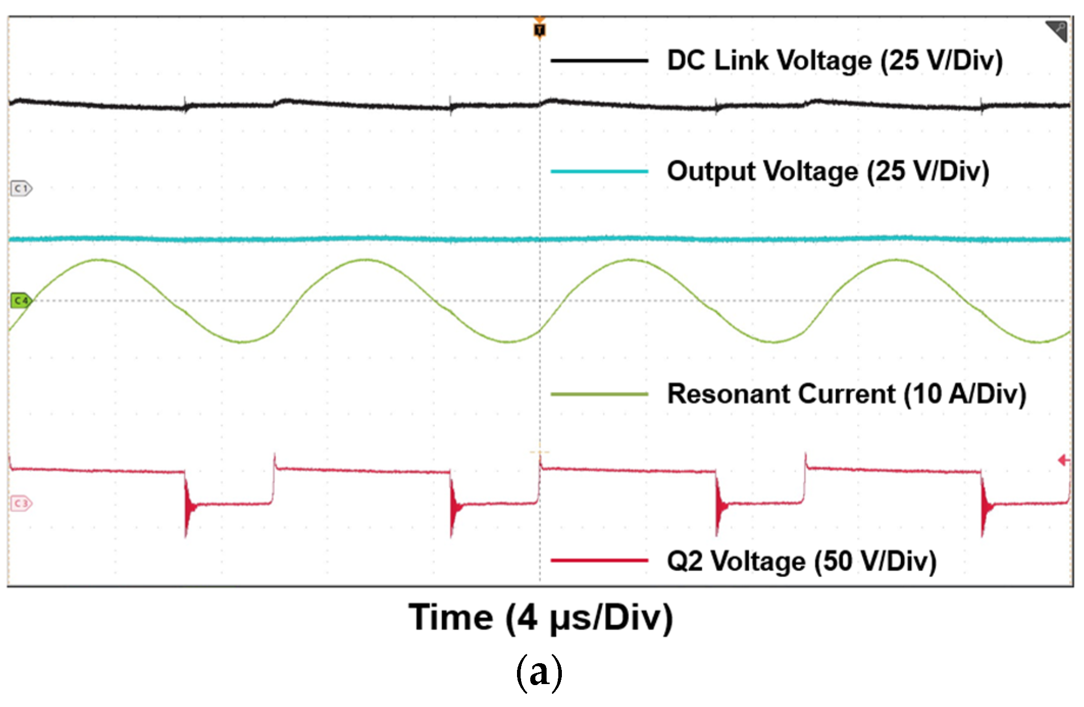
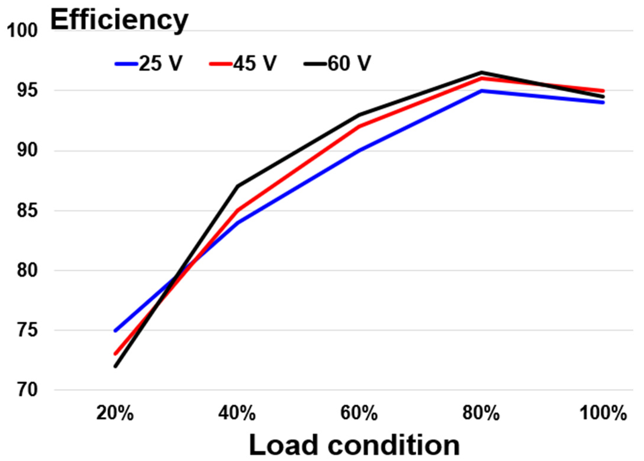
4. Experimental Verification
5. Discussion
5.1. Advantage of Proposed Converter
5.2. Operating Scenarios of Proposed Converter
- 1.
- Photovoltaic (PV) Systems Enhancement:
- 2.
- Battery Charging and Energy Storage Systems:
- 3.
- Electric Vehicle Charging Infrastructure:
6. Conclusions
Author Contributions
Funding
Data Availability Statement
Conflicts of Interest
References
- Marnay, C.; Venkataramanan, G.; Stadler, M.; Siddiqui, A.S.; Firestone, R.; Chandran, B. Optimal Technology Selection and Operation of Commercial-Building Microgrids. IEEE Trans. Power Syst. 2008, 23, 975–982. [Google Scholar] [CrossRef]
- Aslam, A.; Ahmed, N.; Qureshi, S.A.; Assadi, M.; Ahmed, N. Advances in Solar PV Systems; A Comprehensive Review of PV Performance, Influencing Factors, and Mitigation Techniques. Energies 2022, 15, 7595. [Google Scholar] [CrossRef]
- Vigni, V.L.; Manna, D.L.; Sanseverino, E.R.; Di Dio, V.; Romano, P.; Di Buono, P.; Pinto, M.; Miceli, R.; Giaconia, C. Proof of Concept of an Irradiance Estimation System for Reconfigurable Photovoltaic Arrays. Energies 2015, 8, 6641–6657. [Google Scholar] [CrossRef]
- Alajmi, B.N.; Marei, M.I.; Abdelsalam, I.; AlHajri, M.F. Analysis and Design of a Multi-Port DC-DC Converter for Interfacing PV Systems. Energies 2021, 14, 1943. [Google Scholar] [CrossRef]
- Elrefaey, M.S.; Ibrahim, M.E.; Eldin, E.T.; Hegazy, H.Y.; El-Kholy, E.E.; Abdalfatah, S. Multiple-Source Single-Output Buck-Boost DC–DC Converter with Increased Reliability for Photovoltaic (PV) Applications. Energies 2023, 16, 216. [Google Scholar] [CrossRef]
- Verbytskyi, I.; Lukianov, M.; Nassereddine, K.; Pakhaliuk, B.; Husev, O.; Strzelecki, R.M. Power Converter Solutions for Industrial PV Applications—A Review. Energies 2022, 15, 3295. [Google Scholar] [CrossRef]
- Kim, H.; Yu, G.; Kim, J.; Choi, S. PV String-Level Isolated DC–DC Power Optimizer with Wide Voltage Range. Energies 2021, 14, 1889. [Google Scholar] [CrossRef]
- Siouane, S.; Jovanović, S.; Poure, P. Open-Switch Fault-Tolerant Operation of a Two-Stage Buck/Buck–Boost Converter With Redundant Synchronous Switch for PV Systems. IEEE Trans. Ind. Electron. 2019, 66, 3938. [Google Scholar] [CrossRef]
- Urtasun, A.; Lu, D.D.-C. Control of a Single-Switch Two-Input Buck Converter for MPPT of Two PV Strings. IEEE Trans. Ind. Electron. 2015, 62, 7051. [Google Scholar] [CrossRef]
- Leppäaho, J.; Suntio, T. Characterizing the Dynamics of the Peak-Current-Mode-Controlled Buck-Power-Stage Converter in Photovoltaic Applications. IEEE Trans. Power Electron. 2014, 29, 3840. [Google Scholar] [CrossRef]
- Aghdam, F.H.; Abapour, M. Reliability and Cost Analysis of Multistage Boost Converters Connected to PV Panels. IEEE J. Photovolt. 2016, 6, 981. [Google Scholar] [CrossRef]
- Singh, K.A.; Prajapati, A.; Chaudhary, K. High-Gain Compact Interleaved Boost Converter With Reduced Voltage Stress for PV Application. IEEE J. Emerg. Sel. Top. Power Electron. 2022, 10, 4763. [Google Scholar] [CrossRef]
- Ahmad, M.W.; Gorla, N.B.Y.; Malik, H.; Panda, S.K. A Fault Diagnosis and Postfault Reconfiguration Scheme for Interleaved Boost Converter in PV-Based System. IEEE Trans. Power Electron. 2021, 36, 3769. [Google Scholar] [CrossRef]
- Das, D.; Madichetty, S.; Singh, B.; Mishra, S. Luenberger Observer Based Current Estimated Boost Converter for PV Maximum Power Extraction—A Current Sensorless Approach. IEEE J. Photovolt. 2019, 9, 278. [Google Scholar] [CrossRef]
- Chandra Mouli, G.R.; Schijffelen, J.H.; Bauer, P.; Zeman, M. Design and Comparison of a 10-kW Interleaved Boost Converter for PV Application Using Si and SiC Devices. IEEE J. Emerg. Sel. Top. Power Electron. 2017, 5, 610. [Google Scholar] [CrossRef]
- Callegaro, L.; Ciobotaru, M.; Pagano, D.J.; Turano, E.; Fletcher, J.E. A Simple Smooth Transition Technique for the Noninverting Buck–Boost Converter. IEEE Trans. Power Electron. 2018, 33, 4906–4915. [Google Scholar] [CrossRef]
- Zhang, Y.; Cheng, X.-F.; Yin, C. A Soft-Switching Non-Inverting Buck–Boost Converter with Efficiency and Performance Improvement. IEEE Trans. Power Electron. 2019, 34, 11526–11530. [Google Scholar] [CrossRef]
- Cong, L.; Liu, J.; Lee, H. A High-Efficiency Low-Profile Zero-Voltage Transition Synchronous Non-Inverting Buck-Boost Converter with Auxiliary-Component Sharing. IEEE Trans. Circuits Syst. I Regul. Pap. 2019, 66, 438–449. [Google Scholar] [CrossRef]
- Kanathipan, K.; Lam, J. A High Voltage Gain Isolated PV Micro-Converter with a Single-Voltage Maximum Power Point Tracking Control Loop for DC Micro-Grid Systems. IEEE J. Emerg. Sel. Top. Ind. Electron. 2022, 3, 755–765. [Google Scholar] [CrossRef]
- Goyal, V.K.; Shukla, A. Isolated DC–DC Boost Converter for Wide Input Voltage Range and Wide Load Range Applications. IEEE Trans. Ind. Electron. 2021, 68, 9527–9539. [Google Scholar] [CrossRef]
- Hassan, T.-U.; Abbassi, R.; Jerbi, H.; Mehmood, K.; Tahir, M.F.; Cheema, K.M.; Elavarasan, R.M.; Ali, F.; Khan, I.A. A Novel Algorithm for MPPT of an Isolated PV System Using Push Pull Converter with Fuzzy Logic Controller. Energies 2020, 13, 4007. [Google Scholar] [CrossRef]
- LaBella, T.; Lai, J.-S. A Hybrid Resonant Converter Utilizing a Bidirectional GaN AC Switch for High-Efficiency PV Applications. IEEE Trans. Ind. Appl. 2014, 50, 3468–3475. [Google Scholar] [CrossRef]
- Shen, Y.; Wang, H.; Shen, Z.; Yang, Y.; Blaabjerg, F. A 1-MHz Series Resonant DC–DC Converter with a Dual-Mode Rectifier for PV Microinverters. IEEE Trans. Power Electron. 2019, 34, 6544–6564. [Google Scholar] [CrossRef]
- Tang, C.-Y.; Wu, H.-J.; Liao, C.-Y.; Wu, H.-H. An Optimal Frequency-Modulated Hybrid MPPT Algorithm for the LLC Resonant Converter in PV Power Applications. IEEE Trans. Power Electron. 2022, 37, 944–954. [Google Scholar] [CrossRef]
- Wu, F.; Wang, K.; Luo, S. Hybrid-Three-Level Current-Fed Series-Resonant Isolated DC-DC Converter and its Optimization Modulation Strategy. IEEE Trans. Power Electron. 2022, 37, 196–205. [Google Scholar] [CrossRef]
- Gu, L.; Zhang, X.; Li, P. Hybrid-PWM-Controlled Current-Fed Bidirectional Series Resonant Converter with Low Current Ripple and Wide Voltage Gain. IEEE Trans. Ind. Electron. 2021, 68, 7125–7136. [Google Scholar] [CrossRef]
- Wu, H.; Sun, K.; Li, Y.; Xing, Y. Fixed-Frequency PWM-Controlled Bidirectional Current-Fed Soft-Switching Series-Resonant Converter for Energy Storage Applications. IEEE Trans. Ind. Electron. 2017, 64, 6190–6201. [Google Scholar] [CrossRef]
- Xu, J.; Sun, Y.; Xu, G.; Liang, X.; Su, M. Current-Fed LC Series Resonant Converter with Load-Independent Voltage-Gain Characteristics for Wide Voltage Range Applications. IEEE Trans. Power Electron. 2021, 36, 11509–11522. [Google Scholar] [CrossRef]


| Parameter | Value | |
|---|---|---|
| PV voltage | Open circuit | 49.5 V |
| MPP | 15–42.1 V | |
| Maximum Power of PV | 455 W | |
| Output Voltage of MLPE | <80 V | |
| Maximum short circuit current | 15 A | |
| Maximum efficiency | 97.5% | |
| Parameter | Value |
|---|---|
| Maximum Power | 500 W |
| Input Voltage Range | 15–60 V |
| Voltage Gain | 1–3 |
| Output Voltage | <80 V |
| Duty Control Range | 0.5–0.75 |
| Resonant Frequency (Fr) | 100 kHz |
| Maximum Switching Frequency | 150 kHz |
| Resonant Inductance | 66.8 μH |
| Resonant Capacitance | 37.8 nF |
| Input Inductance | 5 μH |
Disclaimer/Publisher’s Note: The statements, opinions and data contained in all publications are solely those of the individual author(s) and contributor(s) and not of MDPI and/or the editor(s). MDPI and/or the editor(s) disclaim responsibility for any injury to people or property resulting from any ideas, methods, instructions or products referred to in the content. |
© 2023 by the authors. Licensee MDPI, Basel, Switzerland. This article is an open access article distributed under the terms and conditions of the Creative Commons Attribution (CC BY) license (https://creativecommons.org/licenses/by/4.0/).
Share and Cite
Kim, B.; Park, H.-P. Non-Isolated Current-Fed Series Resonant Converter with Hybrid Control Algorithms for DC Microgrid. Energies 2023, 16, 6029. https://doi.org/10.3390/en16166029
Kim B, Park H-P. Non-Isolated Current-Fed Series Resonant Converter with Hybrid Control Algorithms for DC Microgrid. Energies. 2023; 16(16):6029. https://doi.org/10.3390/en16166029
Chicago/Turabian StyleKim, Byungki, and Hwa-Pyeong Park. 2023. "Non-Isolated Current-Fed Series Resonant Converter with Hybrid Control Algorithms for DC Microgrid" Energies 16, no. 16: 6029. https://doi.org/10.3390/en16166029
APA StyleKim, B., & Park, H.-P. (2023). Non-Isolated Current-Fed Series Resonant Converter with Hybrid Control Algorithms for DC Microgrid. Energies, 16(16), 6029. https://doi.org/10.3390/en16166029