1. Introduction
DC microgrids have become more popular in recent years as an effective way to distribute and use the electrical energy received from renewable energy sources like photovoltaic systems. Interestingly, the power electronic converters perfectly match the intermediate voltage level and are a crucial component of modern microgrid systems [
1]. High-gain DC–DC conversions are utilized in a variety of applications, such as fuel cells, Base Transceiver Station (BTS) loads [
2], and transportation [
3]. There are a variety of architectures for high-output DC–DC converters utilized in various applications. Still, several difficulties arise when the conversions are operated under high-stress conditions. DC conversions with a power amplifier often have a low-power side with a large input signal and an active electrical side with lower power. It requires switching devices with reduced ON state impedance and diodes with a strong reverse-bias voltage to boost efficiency.
High-gain-ratio conversions are available but they have many drawbacks, including huge switching devices and elements. There are various possibilities for connecting photovoltaic power to DC converters, including series, paralleled, or both [
4,
5,
6]. When panels are connected in a series manner, partial shadowing is avoided, power mismatching between parallel strings is minimized, and fewer blocking transistors are required. The photovoltaic module’s voltage level varies with solar irradiance, and the PV voltage is controlled by a converter for the best power production. The DC–DC converter’s outputs are kept at a constant potential with the connection to the corrected AC grid’s shared DC link [
7]. Furthermore, the BTS’s DC voltage is supplied to the network by a controlled DC–DC converter, resulting in legal constraints. A bi-directional conversion is also adopted to regulate the Battery Energy-Storing System (BESS). When using traditional boost conversions for high power density, the duty cycle must be high, resulting in significant ripple current and low system voltage on switching. Numerous different high-power-gain DC–DC topologies have been published for connecting the PV array. Non-isolated and isolated converters are two categories of high-amplitude converters that employ high-frequency transducers.
DC conversions with a voltage source inverter isolation and terminal voltage step-up are also available. Flyback full-bridge converters and half-bridge, push–pull inverters are separated by unidirectional large step-up DC transformers [
8]. In [
9], a high-amplitude converter with a transformer-connected dual input layout was proposed. Here, an inductor is presented for connecting the battery to a high-voltage terminal in a solar power system. Switching capacitors and inductor-based DC–DC converters use the overlapping approach to obtain large conversion ratios and lower input current distortion. Numerous works exist in the literature related to the proposed topic, certain drawbacks, including complexity issues, the need for special concerns, practically non-feasible characteristics, numerous restrictions, and high losses. Moreover, the conditions of increased system voltage demand high-rated switches. Added to this, high efficiency is achieved only with multiple diode–capacitor steps. Considering these issues, a novel converter with bi-directional operational mode and optimized control is proposed in this paper.
The main contributions of this research are given below.
A high-gain bi-directional DC–DC converter of the reduced count of components is designed in this article, thereby reducing system complexity.
An optimization model is also presented to improve the simulation outcomes of the introduced system, providing feasible characteristics.
The simulation outcomes are verified, and the outcomes show the higher performance of the proposed system by generating improved efficiency and voltage gain.
The structure of the research is listed in
Section 2 and illustrates the background of DC–DC converters, whereas the proposed converter for photovoltaic systems (HGBC-PVS) is designed and illustrated in
Section 3.
Section 4 discusses the software analysis and the system’s effectiveness.
Section 5 shows the conclusion with future scope.
2. DC–DC Converters—Background
When a transformer is used in an isolated conversion, the circuit becomes more complicated and oversized. Furthermore, the leakage current of the transformer causes a high voltage rise in semiconductor circuits. Such issues are avoided using non-isolated conversions, which avoid the usage of transformers. The suggested conversion in [
10] is a non-isolated converter, which is more effective and smaller in size. High gain can be achieved with switching capacitors (SCs) and inductors (L), but these add complexity in high-power situations. In [
11], an inductor minimized the circuit complexity while increasing gain and reducing ripple current. Its design has a large voltage increase and can handle a lot of power but is not flexible and is subjected to increased electromagnetic interference. Using the approach suggested in [
12], a high-gain converter with model predictive control was designed for increased voltage applications. The introduced converter exhibits superior advantages when compared to transformer-less counterparts but does not support variable switching frequency.
A high-efficiency converter was developed in [
13], adopting the concept of gain cell. Even though the proposed converter exhibits slightly better results, the issues related to power density and cost have to be considered. A hybrid-connected three-port converter was proposed in [
14] with reduced voltage stress and soft switching. However, the generated bi-directional port voltages are not so accurate.
Conventional boost converters can produce an unlimited boosting ratio in ideal conditions, but this is not the practice case. Many studies have achieved great step-up capability with high efficiency [
15]. A non-isolated DC–DC conversion is a cascaded enhanced conversion that increases the low-voltage source without needing a large switching frequency. However, a high-rated switch is necessary due to the high-voltage system. Topologies that use a switching inductor and a switching capacitor can provide a high amplifying ratio without requiring a maximum duty cycle. Another improvement to attain great step-up capabilities is the voltage-lift approach. It offers several benefits, including minimal system voltage on the electronic element and electrical gain. However, numerous diode–capacitor steps are necessary whenever the conversion efficiency is very big. Intermediary conversion is crucial for the proper functioning of a DC converter. A traditional boost converter results in severe restrictions, such as diode reversal recovery and unacceptably greater losses during step-up operations. Non-isolated high-output power converters easily solve these limitations.
Voltage multiplier cells (VMCs) are combined with an MPPT to improve the high gain and reduce voltage stress between the power components. However, numerous cells are necessary for achieving high step-up ratios [
16]. Moreover, increased power absorption across more components lowers the total conversion effectiveness. Quadratic boost converters (QBCs) are made by carefully stacking the well-known boost converters, resulting from the first framework feeding the second. As a result, the switch of QBCs is subjected to the same operating voltage as the terminal voltage. Hence, the switching stress is particularly high during the circuit operation. Added to this, the increased leakage current due to the increased voltage stress makes the QBC non-applicable for conditions that demand a conversion ratio greater than 10.
An interleaved construction improves the power controllability of a conventional boost converter or other derivative converters [
17]. Existing stress on the switching converter is reduced because the overall input power is shared among the overlapping phases. Furthermore, the current flowing is smooth and devoid of ripples by properly performing the phase-shift of switching used in each interleaved stage. The working duty cycle of the switching process and the issues related to excessive duty ratios limit the voltage output of the architecture. Coupled inductors (CIs) are utilized instead of isolated inductors to improve the voltage output and converter-generated interleaved structures. The switching frequency required in CI-based conversions is readily satisfied by appropriately altering the switching frequency of the CIs.
Microgrid applications use various DC–DC converters. A DC–DC converter with a multiport is suggested in [
18] for microgrid applications. The author of this study conducted research to minimize many conversions and components, and a thorough analysis was conducted. Yet, this architecture produces a low output while using more switches and passive parts than usual. To sustain the boosted output voltage with high frequency in the Dual Active Bridge converter, a new control method is used [
19]. This technique cannot be used in a non-linear system because classical techniques were used to construct the controller. In [
20], a converter with an extremely high gain was suggested. The gain of the proposed structure is six-times greater, but the circuit does not employ inductance components.
An explanation and demonstration of a DC microgrid with solar PV integration was presented in [
21]. An efficiency of 92.3% for the hybrid combination’s full load capacity was achieved. In this study, there are six operational modes and six switching devices, each of which suffers increased stress. For use with renewable grid applications, a reconfigurable structure was suggested in [
22].
This configuration is utilized to link a variety of regenerative loads; however, additional diodes and capacitors are used for more operating modes.
3. Proposed Converter Topology
Bi-directional conversions transmit power in both directions between two DC sources. The bi-directional DC–DC converters are widely utilized in various applications, including large fuel, hybrid cars, and uninterruptible power sources. These devices are constantly backed up and sustained by rechargeable resources like batteries. At the standard level, a bi-directional DC conversion is necessary to allow for energy flow in both directions. These converters are ready to step forward or backward and transfer voltage levels between their input and output. The bi-directional conversion sends photovoltaic energy to the system when the DC bus power is reduced.
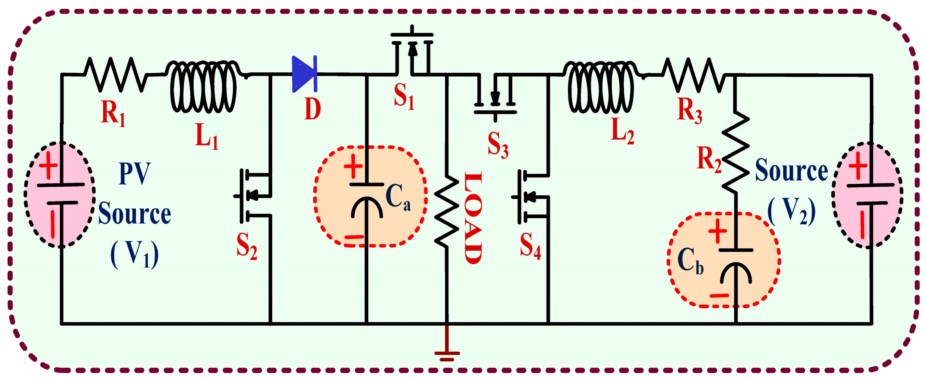
The bi-directional DC–DC converter is shown in
Figure 1. The circuit uses inductors, resistors, capacitors, diodes, and switches with two power supplies. The bi-directional model enhances the voltage gain. The boosting conversion is the first part of the network, while the reversible converter is the latter. To balance the inherent resistance level of the photovoltaic panel with the resistance of the loads, any converter (Speed, Bow, or Buck-boost) is utilized, which leads to the transfer of high energy. MPPT is attained by adjusting the switching frequency ratio of the DC converters, allowing the PV panel to function at its full capacity. The duty cycle is changed by the MPPT algorithms, whereby the PV array functions at the voltages corresponding to the highest power. In most cases, the supply to the power converter is a steady input voltage in locations other than photovoltaic. The duty factor is computed based on the amplification and the circuit characteristics are determined based on the permissible ripple spectrum.
First, the boost conversion must be designed to meet the required charge output voltage. The boosted converter’s functionality is tested by adjusting the load to a continuous power level. The loading currents and voltages change when the load voltages increase, but the converter’s terminal voltage and line current should remain the same. If there is a difference, it implies the existence of losses. The reversible DC conversion is the next level, which can function in both forward and backward directions.
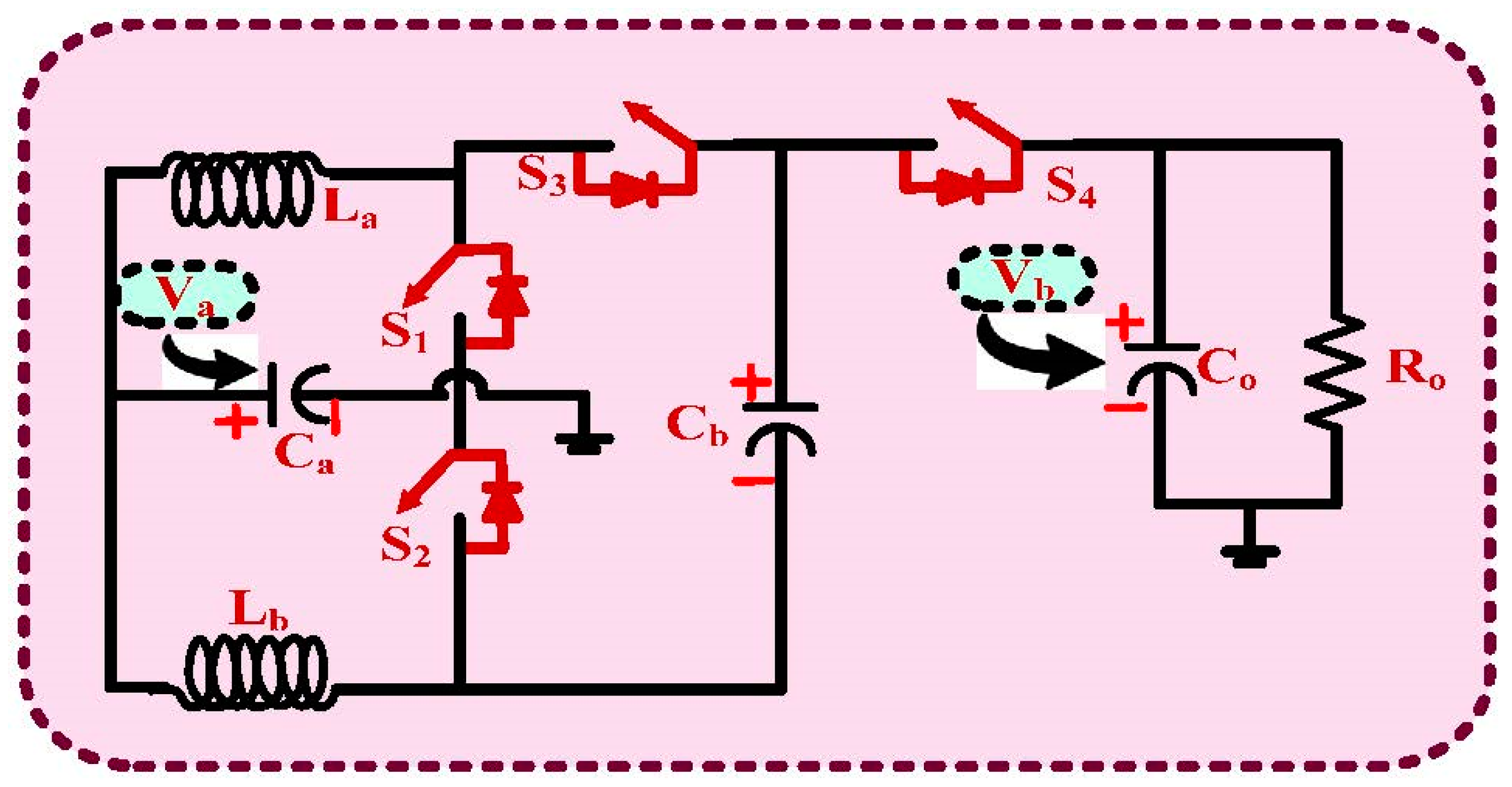
3.1. Bi-Directional Converter Circuit
One of the most well-known varieties of DC conversion is the bi-directional DC–DC conversion. It can conduct buck and boost operations, invert the circulating current orientation, and transmit power among two DC supplies. When charging the battery, it operates in buck style, and when discharging energy to the system, it operates in boost mode. This architecture includes a non-isolated bi-directional converter for the battery-charging process sectors. Two switches control the bi-directional energy supply for recharging and draining the batteries. A MOSFET is employed as a switch in this case.
In the above-mentioned proposed topology, two DC supplies are indicated as V1 and V2. V1 represents the solar PV panel while V2 represents the battery. Since the PV system’s power flow is primarily determined by poor weather, if PV generates higher electricity than the power demands. In this case, the excess energy is stored and should be utilized during the evening and in the event of weather-related changes. These conversions are commonly employed in hybrid energy circuits and energy storage solutions.
The bi-directional translation is carried out via two switches, which perform the control operation. Switch S1 is on during charging mode, whereas switch S2 is off in buck operation. In the first region of operation, the capacitor is charged to deliver the load at the boost level. Therefore, the S1 switch will be off, so, in this condition, switches S1 and S2 will be the series connection.
Cross-conduction concerns do not occur since load shedding is performed according to the set idle time. The outputs are delivered constantly to the load, depending on the demand due to the accessibility of the compensating source. With the aid of bi-directional architecture, the major goal of this suggested system is to deliver uninterruptible supply. The advantages of this proposed work are that it has fewer components, does not need a transformer, is inexpensive, and produces excellent results.
Figure 2 depicts the bi-directional converter design. S1, S2, S3, and S4 are the four switches that are utilised to regulate the converter’s activities. The transistor and diode together function as a relay component. The circuit uses three capacitors: the output capacitor C0, bypass capacitor Cb, and input capacitor Ca. Through a boosted converter controlled by MPPT, the PV component is connected to a lower-voltage bus. At the DC link, the bi-directional conversion is controlled to 48 V. A Voltage Source Converter (VSC) is used to connect the station’s AC to a 230 V AC grid.
This conversion requires the use of a high-sensitivity bi-directional DC conversion because the DC end of the conversion must be maintained at 400 V. This large-gain DC conversion stage permits lower rating valves and other devices in the emitter terminal. As the maximum voltage decreases, the efficacy of the converter increases, but the RDC-ON of switches decreases. The system is also more desirable due to the safety advantages of operating a solar and storage battery at low power.
These overall power practices make sure that the energy is sent to the AC grid when the PV-component-generated electricity exceeds the DC link. In these circumstances, the suggested bi-directional DC transformer works in charging mode converting the low-DC link voltage (48 V) to 400 V to connect to the 230 V AC grid. In contrast to the previous scenario, power must be shifted from the system to the lower-voltage bus necessitating the use of the suggested converter in reverse-biased conditions.
The suggested switching capacitor structure has a high-amplitude bi-directional interlaced boost conversion. To maximise the high gain, the two bi-directional power designs are combined with a switching capacitor, Ca and Cb. S1 and S2 control the converters’ alternating step-up action, while S3 and S4 control the converters’ step-down actions. The DC–DC converter is controlled by an adaptive incremental conductance method. The bi-directional boosting DC–DC conversion is adjusted to keep the DC link voltage () at the required level. If there is surplus power in the DC link, the converter is controlled in charging mode, and if electricity from the grids is required, it operates in the buck method.
3.2. Single-Stage Amplification
It is divided into two sections, one for inductor loading and one for the loading portion. During the on condition of a switch, a DC-link voltage is applied across the inductor, causing its current to grow linearly and, therefore, energizing the inductor. Throughout this time, the load capacitance reverse-biases the diode. When the toggle is switched off, the electricity flows to the loading section via diode
D, exchanging energy between the inductor and the loading area. The energy contained in the resonance is partially transmitted to the capacitance charging. In contrast, the load capacitance is discharged via the load impedance during the inductor’s energizing stage, and
D stands for the duty cycle. The duty cycle is denoted in Equation (1)
The input voltage is denoted
, the output voltage is denoted
, and the duty cycle is denoted as
. The denominator is one, so the power output is greater than the input signal; thus, the step-up chop is named. When the exchange stage is opened, the inductor is de-energized, resulting in a drop in flow
, which creates a voltage spike whose size can be calculated using Equation (2).
The inductor is denoted as
, the current across the inductor is denoted
, and the time is denoted
. Equation (3) can be used to assess the value of inductance.
Here, is duty cycle, is frequency, and resistance is denoted by .
3.3. Derivation of Voltage Gain
The reference voltage is calculated assuming that all the components are perfect. Let V1 be the voltage on the negative side, and V2 is the value on the positive terminal. S3 and S4 are maintained off, whereas S1 and S2 are maintained at a specific rate with a duty cycle of D. S1 and S2 are retained in the OFF state during the buck operations. In contrast, S3 and S4 are driven at a particular intensity with a load current. The suggested bi-directional DC–DC converter’s enhanced operating is investigated in three phases. Switches S3 and S4 employ antiparallel diodes D3 and D4 to free up the energy contained in inductances L1 and L2.
Mode 1: S1 and S2 are ON
This operating method is alternative modes 2 and 3. D3 and D4 are reverse-biased during this state, and the capacitance maintains the load. The charges on inductances L1 and L2 grow, as does the power through the inductances.
Mode 2: When S1 is ON, and S2 is OFF
The voltage across the inductance
throughout this phase is
. Here,
is the voltage applied, and
D indicates the platform’s duty frequency. D4 is on, and D3 is off.
supplies the load, and the corresponding equation is given by,
The input and output voltage are denoted and , and the voltage across the inductor is denoted .
Mode 3: When S1 is OFF and S2 is ON
Transistor D3 is ON, and transistor D4 is OFF. The output voltage equals the inductor voltage and it is represented as
. By simply applying KVL, Equation (5) is obtained.
The input voltage is denoted , the capacitor voltage is denoted , and the voltage across the inductor is denoted . The mean voltage across inductances and is zero during a period T, as per voltage-second balance. Inductor charges throughout the ON condition of the power switch, as indicated by the current and discharging during the OFF phase, as indicated by the lowering current .
For the inductance
, volt-sec balancing is used. The condition is expressed in Equation (6).
The input and capacitor voltage are denoted
and
. The duty cycle and the propagation time are expressed as
. Changing the phrases around, and expressed in Equation (7)
The input voltage is denoted as
and the duty cycle is expressed as
D. Inductance
charged during the ON phase switch S2, as indicated by the growing current
and discharging during the OFF phase, as indicated by the lower current
, for the inductance
, and denoted in Equation (8).
The voltage across the input and resistor
b is denoted as
and
, and the propagation period is
T. Equation (8) can be rearranged and expressed in Equation (9).
Changing the phrases around, the condition is expressed in Equation (10)
The duty cycle is expressed as D. The voltage across the input and resistor b is denoted as and . The state of charging (SoC) is computed for the batteries. The SoC is varied from 0% to 100%. When the battery is fully charged, the SoC is 100%, and when the battery is fully drained, the SoC is 0%. The charging life should be reduced so that the 100% SoC is achieved faster, and the discharging time should be higher so that the SoC takes more time to reach 0% from 100%. Placing the transistor across the switch reduces the flow of current in the cutoff region, which reduces the battery leakage. By adjusting the duty cycle, the SoC of the battery is controlled and adjusted.
3.4. Design of Elements
The ripple power for the interlaced inductors is calculated using the waveforms again for enhancing operation, as expressed in Equation (11)
The deviation in the inductor current is denoted as , and the inductor is denoted L. The inductance value is computed using a 5% fluctuation in the inductance current flow, a loading of 2 kW, and a 100% performance assumption. The inductance value is .
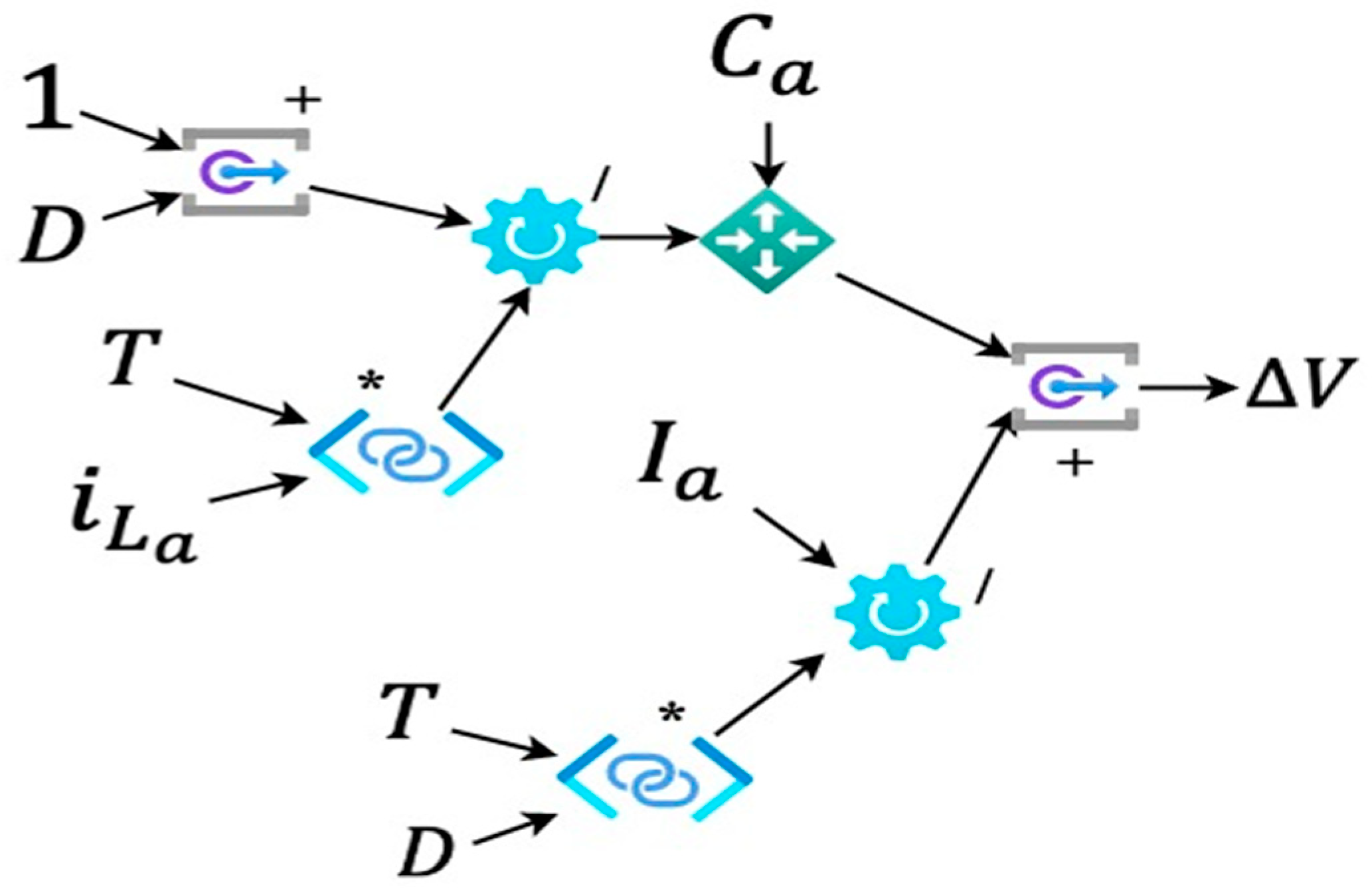
The induced voltage across the capacitance
during S2’s OFF time is expressed in Equation (12)
The total current from the source is denoted , and the input capacitor is denoted . The current at the input inductor is expressed as . The propagation time and duty cycle are expressed as .
A graphical view of the mathematical function
is shown in
Figure 3. The duty cycle, input capacitor, traveling time current at the input inductor, and the total input current are used to compute the function
. This value shows the deviation in the voltage or voltage drop that occurs in the circuit. The voltage fluctuation across output capacitance
is calculated using Equation (13).
The capacitance is set at 50 μF to provide a 5% ripple current. The output capacitance has a value of 100 μF and is intended to handle a 1% ripple current. The propagation time and duty cycle are expressed as . The voltage fluctuation at the input is expressed as .
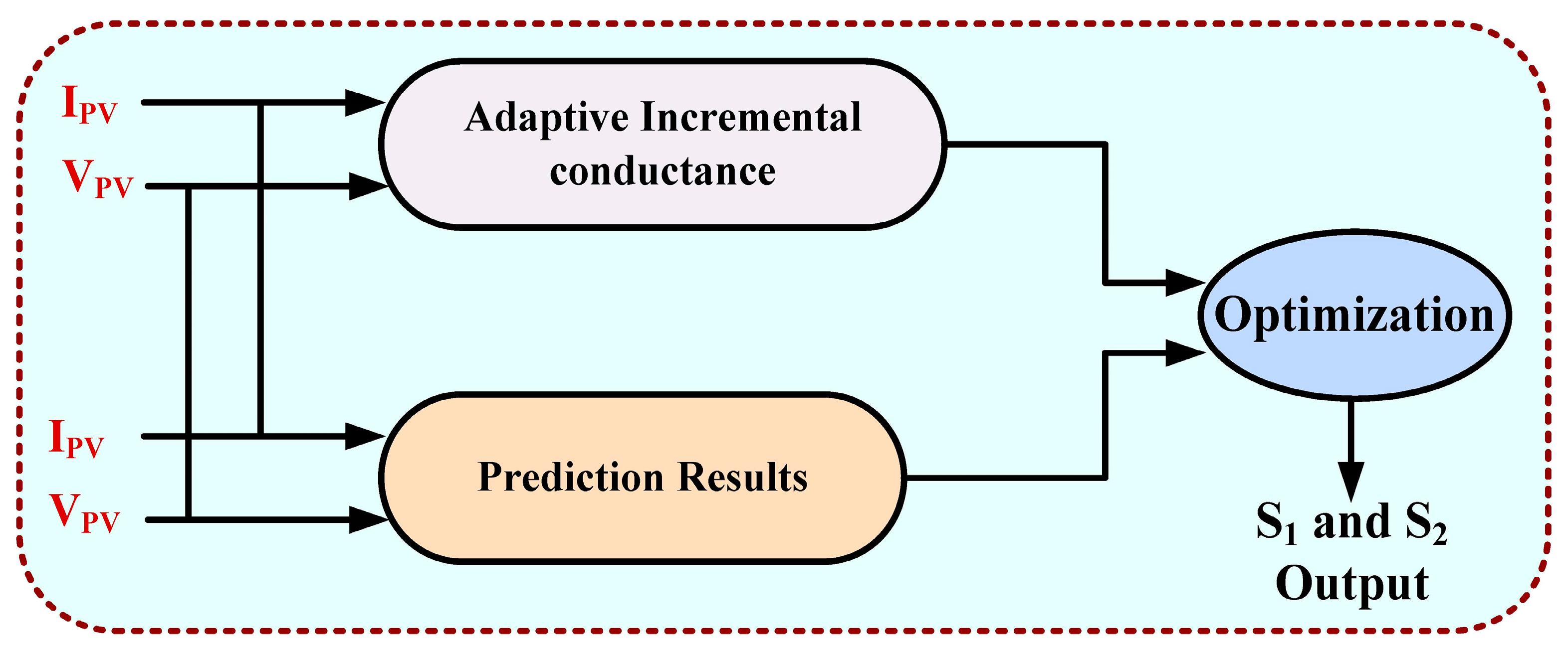
3.5. Optimization Method
It is a better regulator for plants; the plant is a DC–DC converter with several state variables that must be regulated. It sees the plant as a limited collection of linear programming.
The optimal method of the HGBC-PVS system is shown in
Figure 4. The system consists of adaptive incremental conductance-predicted results and a optimization block. Based on the conductance value, the gain of the system is increased. The prediction is used to speed up the computation process. The optimization module reduces the voltage drop in the converter circuit.
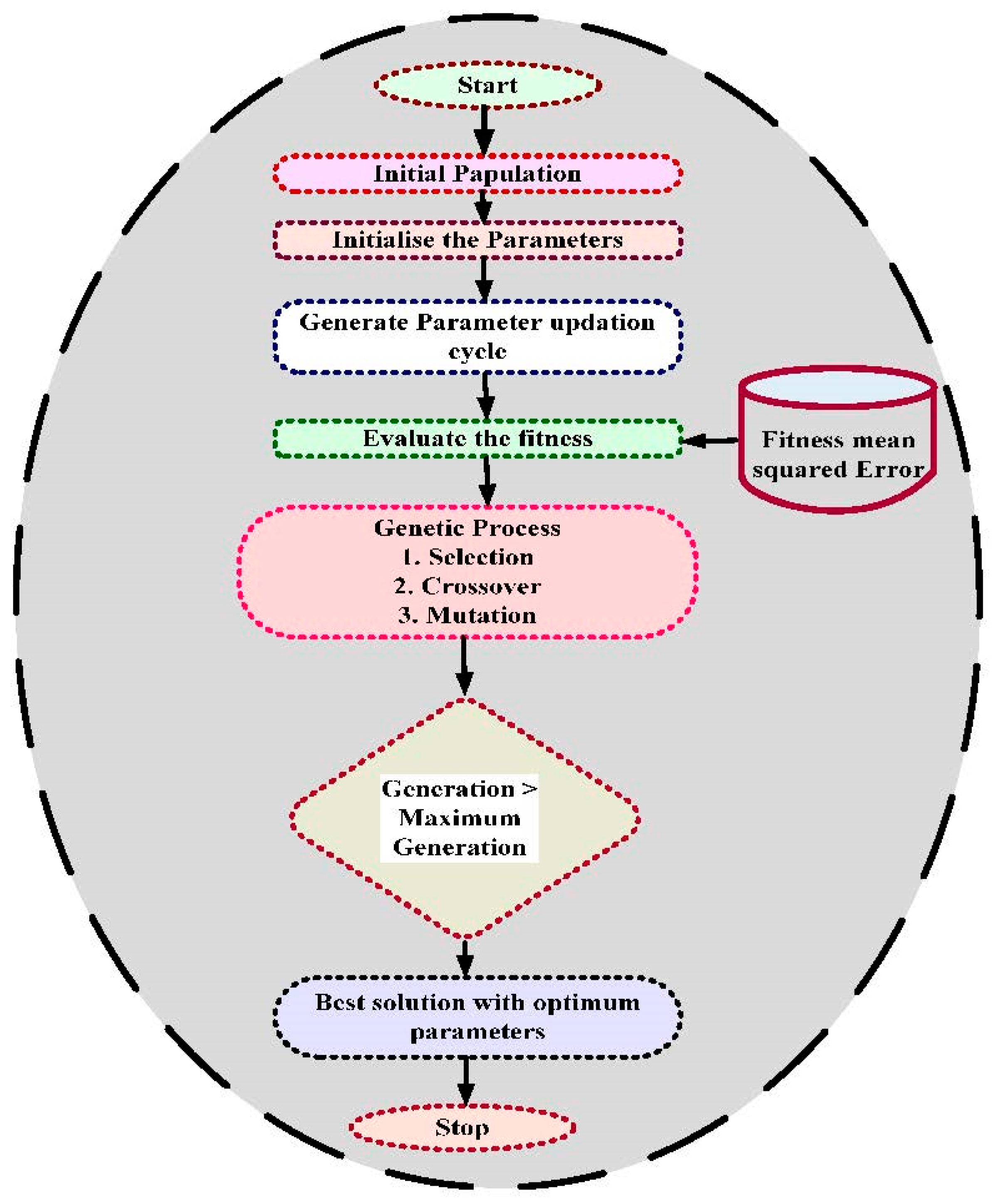
The updating algorithm of the HGBC-PVS system is designed and shown in
Figure 5. The initial population is analyzed, and the parameter values are initialized. The parameter-updating model is computed, and the fitness module for mean squared error is used. The fitness evaluation function is used to analyze and find better results using optimum parameters under the process of selection, crossover, and mutation. The final optimized solution is used for further analysis, and each model depicts a stage of transition. MPC determines the forecast of each switching cycle, and then the computational complexity undergoes the minimizing procedure, and the state with the least error is created and implemented in the plant.
The DC–DC converter is the recommended plant in a photovoltaic and it has two-state variables, owing to the continuous current operation. Three screens are necessary to forecast the future amount of PV power, which would raise the network’s cost and capacity. One voltmeter is removed due to this technology, which lowers the system cost while maintaining performance. The final stage in MPC management is to optimize all potential future situations and choose the best value with the least error.
The cost function is used to optimize and is expressed in Equation (14)
The optimization process, like selection, crossover, and mutation processes, is given in the above flowchart. Correspondingly, the cost function and standard current are denoted by f and . The proposed control method generates the reference current . The PV current is denoted . The scaling factor is denoted . The diagram shows that the algorithm merely senses the PV energy and voltage. It then uses a proposed control technique to build the reference signal in peak power performance. The MPC method starts to control the converter to keep it in sync with the current. The preceding section states that the voltage watcher ignores the battery voltage sensor.
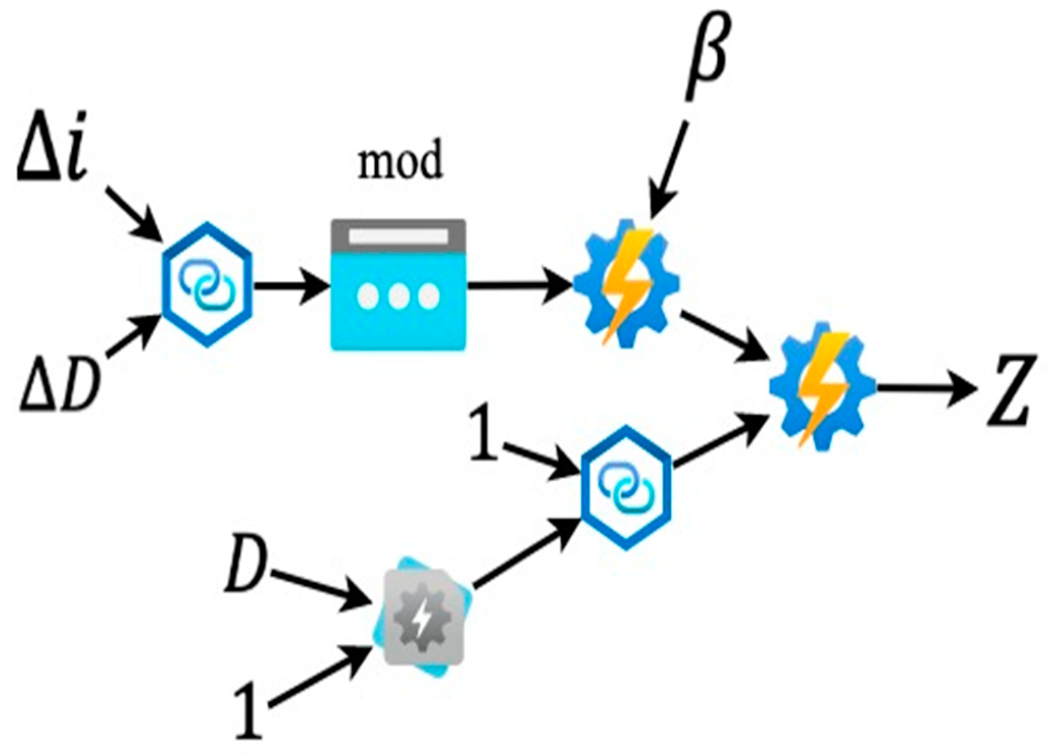
The perturbation step size represented as
Z is set to a constant value to create a constant step length MPPT, or it could be configured to be adaptive using Equation (15).
where
is the change in the present and prior amount of the reference signal,
is the differential between the present and prior value of a PV power supply, and
is a scale parameter.
A graphical model of the mathematical function
Z is shown in
Figure 6. The system uses current deviation, deviation in the duty cycle, the original duty cycle, and the scaling factor
to produce the final result
Z. In this way, the power is optimized in the proposed HGBC-PVS system. The HGBC-PVS system is designed in this section for photovoltaic systems with power optimization. The voltage drop and current variations at the output are reduced by the HGBC-PVS system. In the remaining part, the HGBC-PVS system’s simulation results are examined and evaluated.
Figure 3 represents that, while varying the duty cycle, the changing voltage occurs in the output terminal in the same way.
Figure 6 represents how the overall output is obtained.
Based on the duty cycle of the diode, the overall gain is obtained. The duty cycle ratio changes automatically, like change in the current, change in the voltage, and inductor output. So, the obtained efficiency of this converter is 97.5%, as shown in the comparison table.
4. Simulation Analysis and Performance Comparisons
The suggested converter and the photovoltaic solar networks are modeled and evaluated in the MATLAB 2021B SimPower Networks blocks. The input power is 18 V DC, and the output is tested using a load resistor. Pulse producers with a 180-degree pitch sequence are used to generate the discharge impulses for the switching. A voltage level supply on the positive terminal and a potentiometer on the emitter terminal are used to verify the reverse energy flow. The operating principles are recorded and displayed in MATLAB 2021B environment. The shifting waves are created at a frequency of 10 kHz, with a sample duration of 1 microsecond.
Table 1 indicates the simulation components and parameters used for the analysis. The PV voltage is 15–19 V, the sampling time is 12 μs, and two inductors with 5 mH and three capacitors with 250 μF are used. Four MOSFETs and four diodes are used in the proposed HGBC-PVS system. The circuit is designed, and the outcomes, such as voltage drop, current, efficient, and voltage gain, are computed.
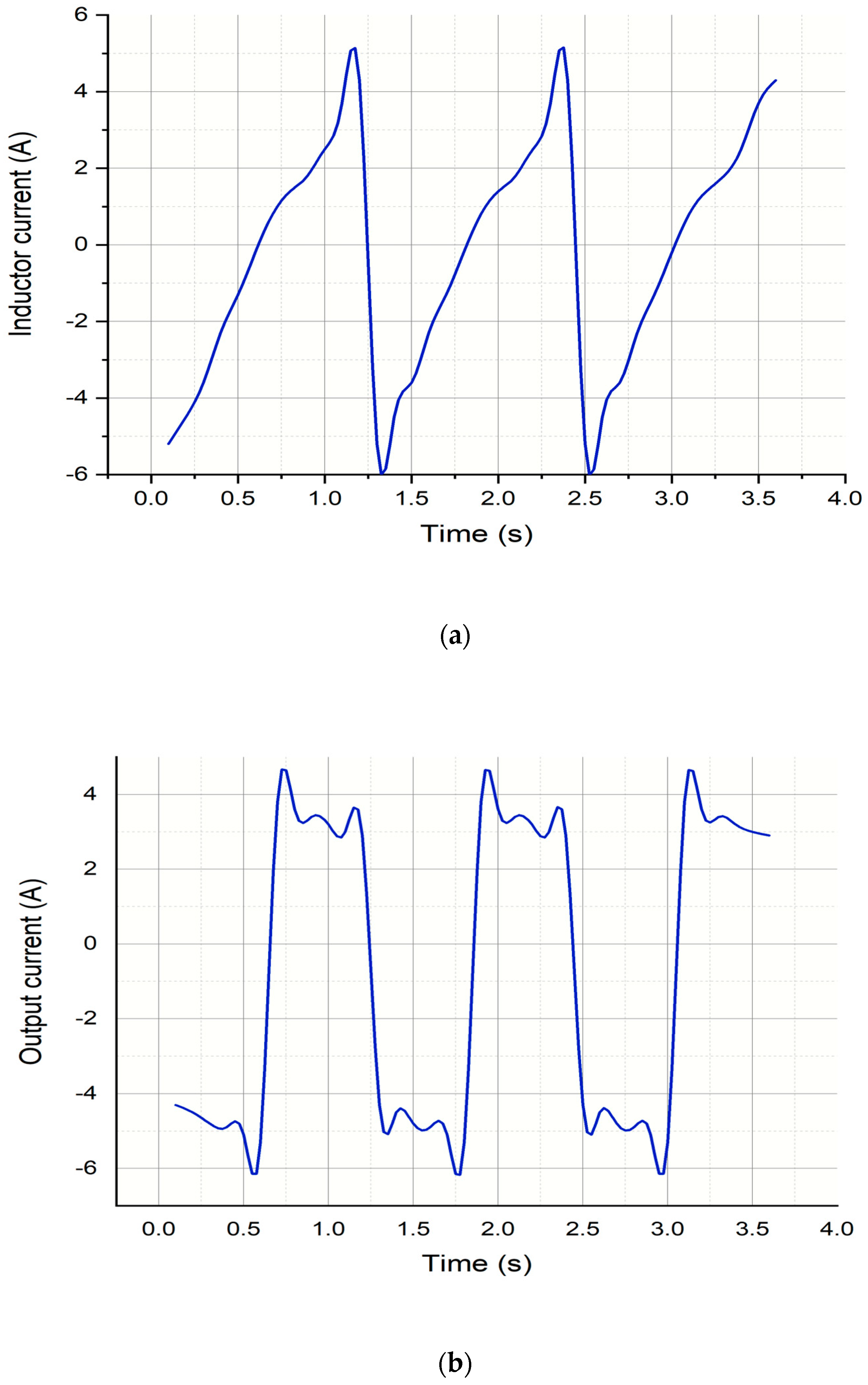
The inductor and output current analysis of the HGBC-PVS system is represented in
Figure 7a,b. The inductor current is analyzed at the input side, and the current at the output is measured across the resistor
. The inductor current graph looks like a trapezoidal function. When the inductor charges, the voltage increases, and when discharging occurs, the inductor voltage reduces. The output current is directly related to the inductor current and, hence, the current exhibits variations. The HGBC-PVS system produces a higher current at the output.
Table 2 indicates the efficiency analysis of the HGBC-PVS system. The measured efficiency and the computed efficiency of the HGBC-PVS system are analyzed and tabulated. The computed efficiency is calculated via
The simulation analysis is conducted by varying the input power from 10 W to 100 W with a step size of 10 W. As the input power increases, the respective efficiency of the measured efficiency decreases, and the computed efficiency also increases. The HGBC-PVS system with an optimized algorithm increases the voltage gain.
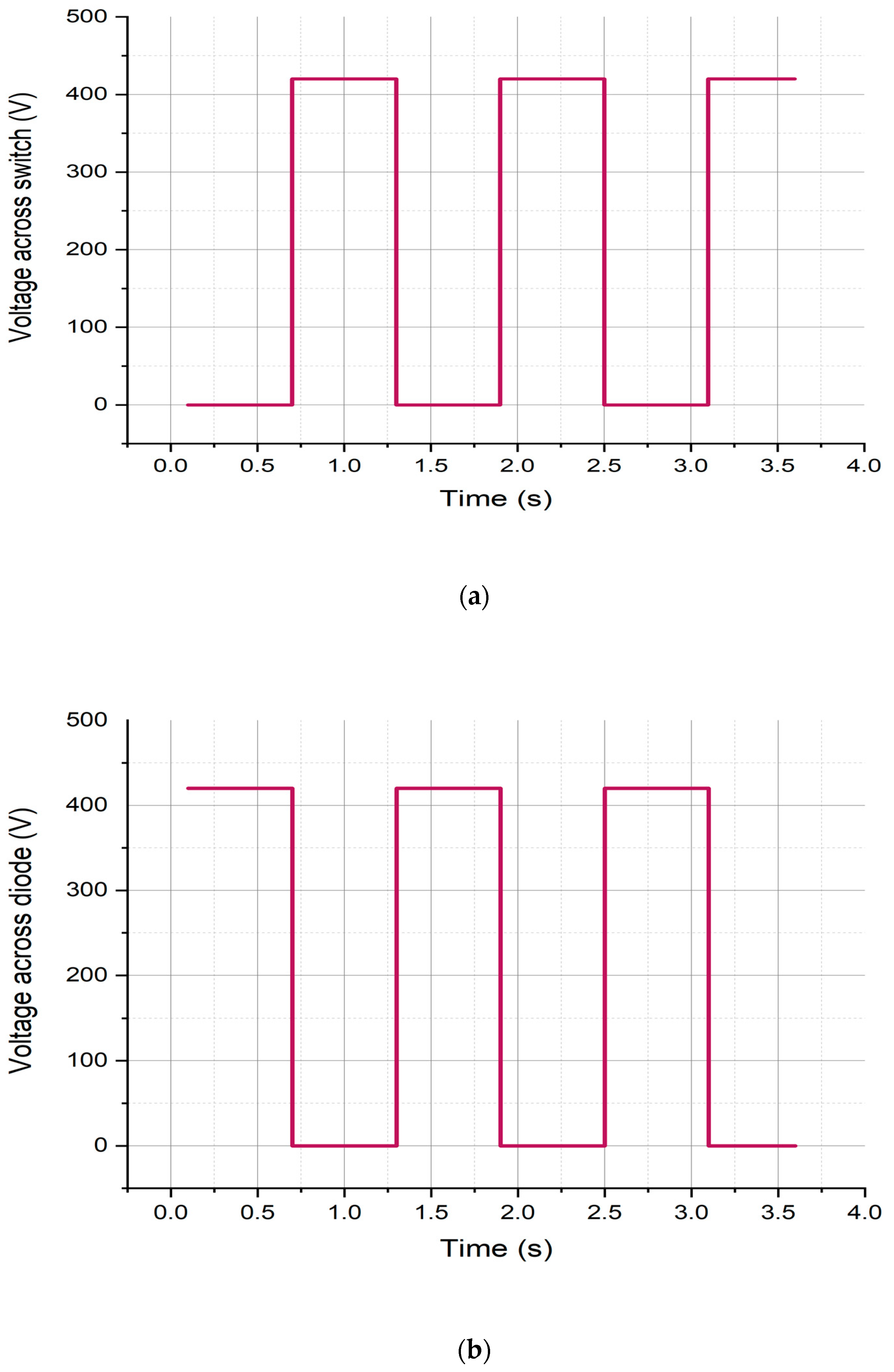
The voltage across the switch and diode analysis of the HGBC-PVS system are shown in
Figure 8a,b. The simulation time is continuously monitored, and the simulation outcome is monitored. The voltage across the switch and the diode is inversely related to each other. The diode is turned off when the switch is on and vice versa. The HGBC-PVS system ensures a high gain, and the system produces an enhanced output voltage. The optimization method reduces the voltage drop and current fluctuations.
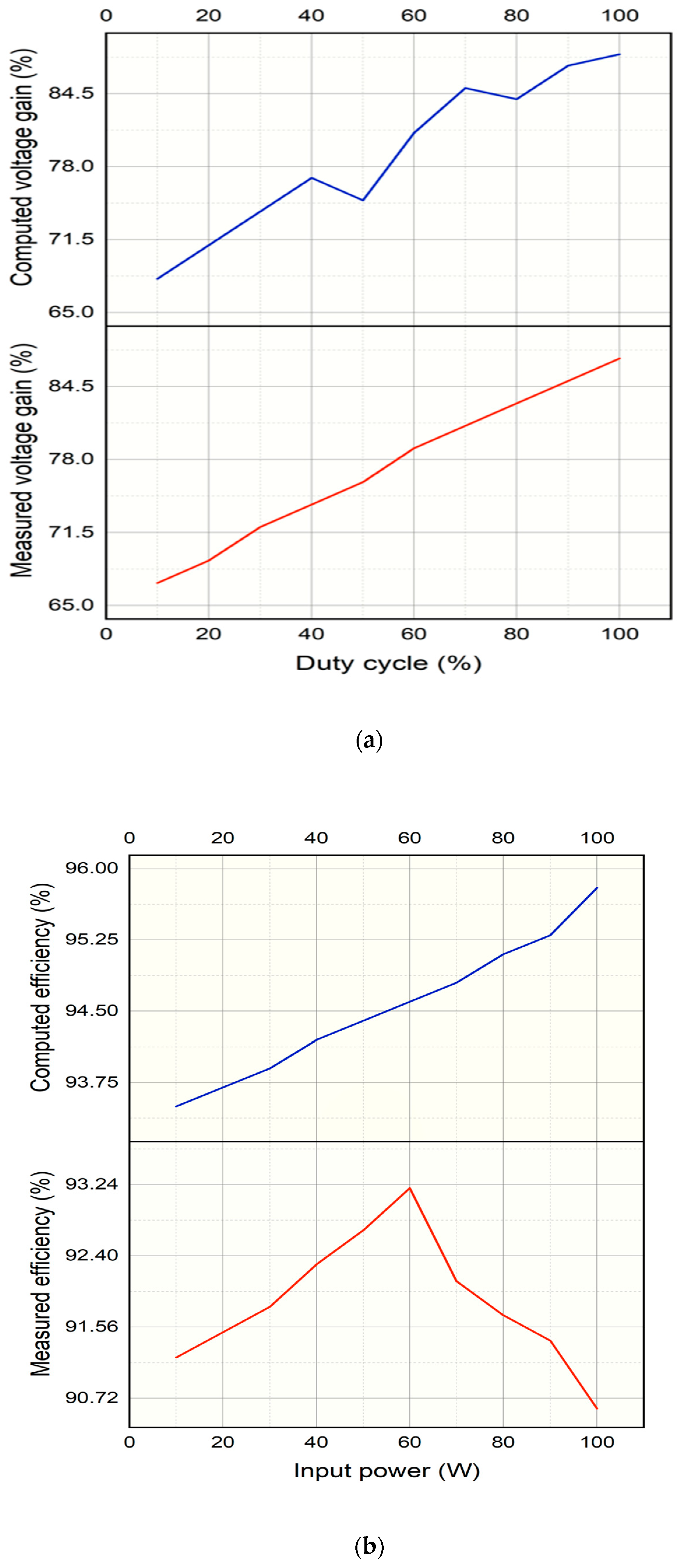
The voltage-gain analysis of the HGBC-PVS system is shown in
Table 3. The simulation outcomes, such as measured voltage gain and computed voltage gain, are attained, and the outcomes are tabulated. In simulation analysis, the duty cycle is varied from 10% to 100% with a step size of 10%. As the duty cycle increases, the on-time of the switch and off-time of the diode increase, which results in a higher duty cycle at the output. The HGBC-PVS system with a higher optimization method reduces the voltage drop and increases the voltage gain. The comparative analysis of existing converters with the proposed model is given in
Table 4.
The voltage and efficiency analysis of the HGBC-PVS system is represented in
Figure 9a,b. The input power for the simulation analysis is varied from 10 to 100 W, with an incremental level of 10 W. The simulation outcomes are compared with the measured results. The measured results are always higher with the optimized method. As the input power increases, the respective efficiency and voltage gain of the HGBC-PVS system also increase. The converter ensures a lesser drop and higher voltage gain in all the simulation environments.
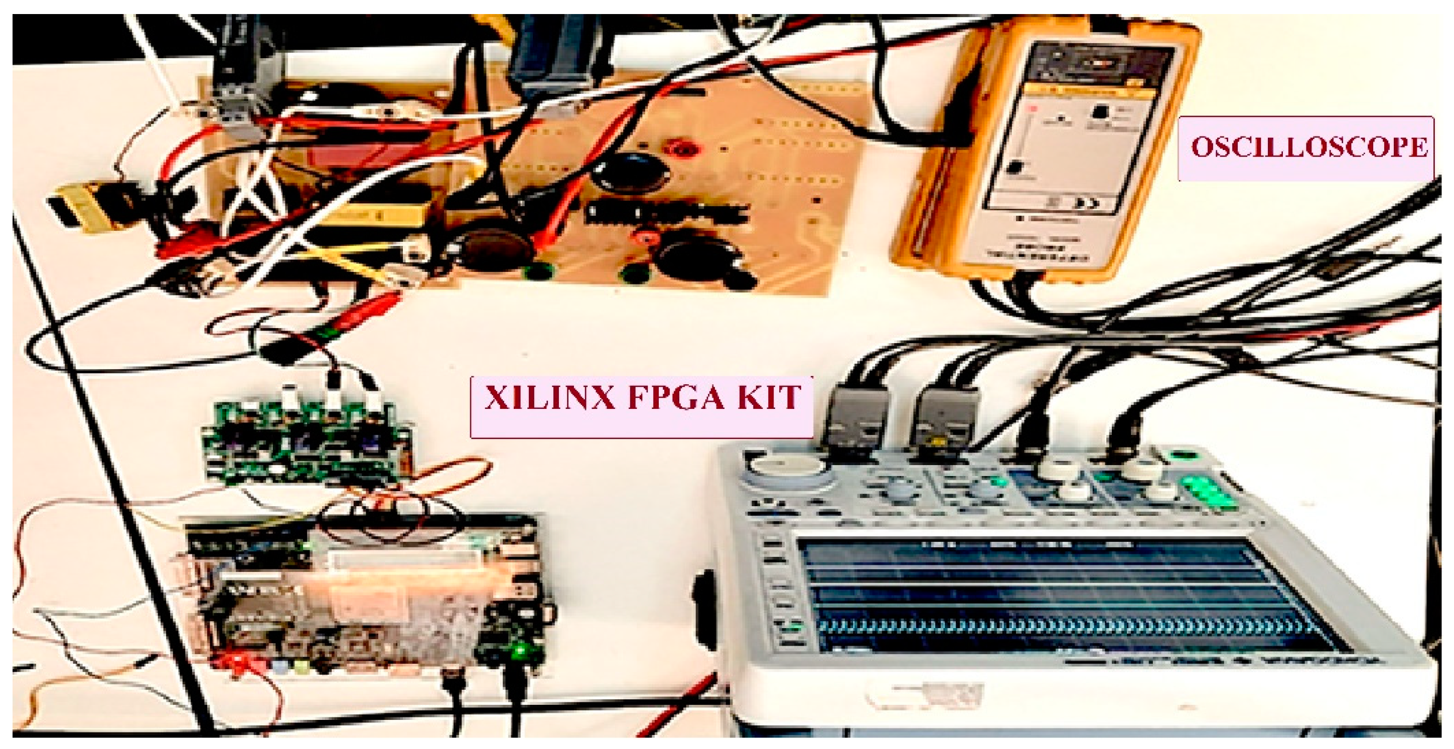
The system output of the real-time system is denoted in
Figure 10. The hardware components are shown, and the system uses optimized parameters. The output of the HGBC-PVS system is verified using the given high-gain DC–DC converters, reducing the system error, and the higher SoC is achieved using the optimized algorithm and parameters. The outcome is measured using Xilinx software for photovoltaic systems.
The HGBC-PVS system is designed and analyzed in this section. The simulation outcomes in terms of voltage across the switch, diode, and current in the inductor, output, efficiency, and voltage gain are computed and compared with the measured results. The HGBC-PVS system with the optimization method reduces the voltage drop and current fluctuations and, thus, increases the system outcomes.


