Article

Effect of GaN-Based Distributed Bragg Reflector on Optical Properties of CH3NH3PbBr3 Crystals

1
Faculty of Electronic information and Electrical Engineering, Dalian University of Technology, Dalian 116024, China
2
School of Physics, Dalian University of Technology, Dalian 116024, China
*
Author to whom correspondence should be addressed.
Energies 2023, 16(12), 4547; https://doi.org/10.3390/en16124547
Submission received: 4 May 2023 / Revised: 2 June 2023 / Accepted: 3 June 2023 / Published: 6 June 2023
(This article belongs to the Special Issue Advanced Materials for Sustainable Energy Applications)

Abstract

:
As a photoelectric material, the luminescent efficiency improvement of organic–inorganic perovskite material is a hot topic. This work fabricated a nanoporous distributed Bragg reflector based on GaN with a periodic structure using electrochemical etching methods. Considering the fact that hybrid perovskite materials are difficult to prepare on an inorganic GaN-based substrate, ultraviolet ozone treatment was implemented to enhance the surface activity of the prepared distributed Bragg reflector substrate. Cubic CH3NH3PbBr3 crystals with smooth surfaces and precise edges were successfully prepared on the ozone-treated distributed Bragg reflector substrate by a two-step immersion method in the air environment. The structural property of the prepared CH3NH3PbBr3 crystals was investigated using X-ray diffraction, scanning electron microscopy and Fourier-transform infrared spectroscopy. The structural analysis results showed that CH3NH3PbBr3 crystals grown on the prepared distributed Bragg reflector and reference substrates have the same structure, with a good crystal quality. The photoluminescence intensity of CH3NH3PbBr3 crystals grown on the distributed Bragg reflector was significantly enhanced. The enhancement is approximately 3.11-fold compared with CH3NH3PbBr3 crystals grown on the unetched reference GaN substrate. Moreover, there is a 7.2 nm spectral blue shift. The enhancement of the photoluminescence intensity could be attributed to the out-coupling of emission light in the prepared crystals, and the blue shift could be attributed to the stress relaxation caused by the nanoporous GaN structure of the distributed Bragg reflector substrate.

1. Introduction

Because of the low production cost and high efficiency, organic–inorganic hybrid perovskite materials have become one of the most popular photoelectric materials in recent years [1,2,3]. In 2009, Miyasaka prepared solar cells using hybrid perovskite materials (CH3NH3PbI3 or CH3NH3PbBr3) as the absorption layer for the first time, realizing a 3.81% photoelectric conversion efficiency (PCE) [4]. Since then, more and more research into hybrid perovskite-based solar cells has been reported and the PCE has increased continuously [5,6,7,8]. This is mainly because this kind of material has the characteristics of simple preparation, large carrier mobility, excellent light absorption ability and great chemical stability [9,10,11,12,13]. On the other hand, hybrid perovskite materials have been used as luminescent materials owing to their excellent photoelectric properties and their direct, adjustable band gaps [14,15,16,17,18]; however, the low luminescence efficiency limits their further development. Recently, researchers have tried to improve the luminescence efficiency of perovskite materials by adjusting the chemical constituent of perovskite materials [18,19]. Yan et al., studied the effect of the CH3NH3Br/PbBr2 ratio on the photoluminescence (PL) intensity of CH3NH3PbBr3 perovskite material, and they found that the PL intensity increases as the MABr/PbBr2 ratio increases [20]. Yan et al., reported the tremendous change of PL intensity in MAPbBr3-xClx only by adjusting the Cl/Br ratio [21]. Using additives is another method to increase the PL intensity for this kind of material. Li et al., introduced different concentrations of Pb(Ac)2 solution into MAPbI3 and observed a significant improvement of fluorescence intensity [22]; they also found that adding a certain proportion of Pb(Ac)2 can promote grain growth, well passivate the film surface, and improve its chemical stability. The previously reported methods to improve the luminescence efficiency of hybrid perovskite materials are basically achieved by changing the chemical composition of the materials. Enhancing the luminescence efficiency of hybrid perovskite materials without changing the structure of the materials, for example, only by changing the substrate, is rarely reported. Moreover, hybrid perovskite materials are easy to degrade under the influence of ambient humidity. Mosconi et al., researched the perovskite/water interface by theoretical simulation and found that surface passivation of perovskite materials and interfacial modification can increase the stability of perovskite materials [23].
Distributed Bragg reflectors (DBRs) are an essential component of optical devices, which have a periodical multilayer structure consisting of two optical materials with diverse refractive indexes [24,25,26]. Reflected lights at diverse interfaces can interfere and combine with each other so that the intensity of reflected lights is enhanced. Various kinds of DBRs based on GaN with a periodic structure have been reported one after another [26,27,28,29,30]. DBRs composed of (Ga, Al, In)N/GaN periodic heterostructures usually need 20 to 40 pairs of heterostructures to obtain a high peak reflectance due to the small contrast of the refractive index [31]. The periodic heterostructures are usually obtained by using the metal organic chemical vapor deposition (MOCVD) method. The large number of pairs and the low growth rate result in a long growth time [32]. Therefore, DBRs with these structures are difficult to use in commercial manufacturing. Recently, Carreno et al., fabricated a DBR by the alternate deposition of silica and titania layers on a glass slide by using electron beam evaporation technology [33]. This kind of DBR can greatly enhance the PL intensity of inorganic cesium lead halide perovskite. In 2020, Xiao’s research group prepared a nanoporous (NP) GaN DBRs sample by using electrochemical (EC) etching methods, which has a lot of advantages, such as low cost, broad area and high reflectivity [26], and they found that the PL intensity of the inorganic CsSnBr1.8I1.2 materials prepared on the DBR substrate presented a 4.3-fold enhancement compared with the films prepared on unetched GaN substrate. DBR have been used in devices as an optical platform to obtain remarkable optical gain and improve the performance of devices, such as light-emitting diodes, lasers and photodetectors [34,35,36].
However, the effects of NP-GaN DBR on the PL intensity of hybrid perovskite crystal material are rarely reported. This is due to the fact that the inorganic GaN-based substrate is hydrophilic rather than lipophilic. At present, the most frequently used preparation method of hybrid perovskite materials is the solution method, usually in a vacuum or inert gas environment. The perovskite materials prepared by using the solution method usually need to be dissolved in organic solvent, and therefore the precursor solution cannot be coated uniformly onto the hydrophilic GaN-based substrate.
In this paper, NP-GaN DBRs were prepared by using the EC etching method. Then, ultraviolet ozone (UV-O3) treatment was implemented to enhance the surfactivity of the prepared DBR substrate. CH3NH3PbBr3 crystals were successfully prepared on the UV-O3 treated NP-GaN DBR substrate by a two-step immersion method in an air environment [16]. The structures of CH3NH3PbBr3 crystals grown on the NP-GaN DBR and reference substrate were investigated by using scanning electron microscopy, X-ray diffraction and Fourier-transform infrared spectroscopy. The PL intensity of CH3NH3PbBr3 crystals grown on the NP-GaN DBR substrate showed a significant enhancement, compared with that of the sample on the reference substrate. Moreover, the PL peak of crystals on the prepared DBR substrate showed a clear blue-shift. The reasons for the PL intensity enhancement and the spectral blue shift were discussed. This work provides an alternative method of improving the PL quantum yield of hybrid perovskite crystals. It may be used in novel design of devices based on hybrid perovskite crystals, such as lasers and light-emitting diodes.

2. Materials and Methods

2.1. Fabrication of NP-GaN DBR

Normally, GaN is grown over an Si substrate using AlN as buffer layer because of the lattice mismatch [37,38]. In this work, the used substrate is c-surface sapphire instead of Si. That is because the Si substrate will be etched during the EC etching process if Si substrate is used. Ten periodic pairs of undoped GaN (u-GaN)/Silicon-doped GaN (n-GaN) layers are grown on a c-surface sapphire substrate with a 2-μm-thickness GaN low-temperature buffer layer by MOCVD method. The thickness of the u-GaN layer is 60 nm while that of the n-GaN is 80 nm, and the doping content of the doped layer is 1 × 1019 cm−3. Figure 1a shows the diagrammatic sketch of the etching process at room temperature using a 9 V etching voltage with a 35 min etching time. Generally, the EC etching originates from surface ‘defects’, e.g., localized nano-scale regions of impurity and high carrier concentration. When pits are formed, substantial numbers of holes gather at the tip of the patch, leading to avalanche breakdown (i.e., formation of nanopores) [39]. The NP-GaN DBR presents a periodic structure, which can be observed in Figure 1b. The reference substrate is an unetched GaN film on the c-surface sapphire substrate. Figure 1c is the high resolution SEM cross-section. Figure 1c shows that the NP-GaN DBR presents a periodic structure. The diameter of the etched pores is in the range of ~10 to ~50 nm. The non-uniform distribution of pore sizes is caused by the non-uniform EC etching process. The porosities of n-GaN and u-GaN layers are about 0% and 50%, respectively.

2.2. Preparation of CH3NH3PbBr3 Crystal on the DBR and Reference Substrate

The prepared DBR and reference substrates were wiped with anhydrous ethanol several times until the surfaces were clean and free of other impurities, and then they were placed in a UV-O3 chamber with a 15 min processing time. Figure 2 shows the preparation process diagram of CH3NH3PbBr3 crystals. All the substrates were moved onto a heating platform and kept at 50 °C for 15 min. The CH3NH3PbBr3 crystals were prepared by using the soak method. To obtain a Pb(Ac)2 saturated solution, 40 mg of lead acetate trihydrate (Pb(Ac)2·3H2O, 99%, Sigma) was dissolved in 300 μL methanol. To obtain a 5 mg/mL solution of CH3NH3Br/IPA, 40 mg of bromide methylamine (CH3NH3Br, 99.5%, Xi’an Polymer Light Technology Corp., Xi’an, China) powder was dissolved in super-dry isopropanol (IPA, C3H8O, 99.5%, J&K Scientific, Beijing, China). Then, 40 µL Pb(Ac)2 saturated solution was drop-casted onto the NP-GaN DBR and reference substrates. After that, the substrates were transferred to a heating platform and were annealed at 65 °C for 30 min in an atmosphere environment. After natural cooling, the substrate was placed into the 5 mg/mL solution of CH3NH3Br/IPA, with the coated side facing up. The reaction continued unabated for ~28 h. The prepared CH3NH3PbBr3 crystals were washed gently by super-dry IPA and then put into a vacuum drying oven at 32 °C for 12 h.

2.3. Materials Characterization

The morphologies of the CH3NH3PbBr3 crystals were investigated by scanning electron microscopy (SEM 450, FEI, Thermo Fisher, Waltham, MA, USA). The structural properties of the prepared CH3NH3PbBr3 crystal were investigated by X-ray diffraction (XRD, Shimadzu, Japan) and Fourier-transform infrared spectroscopy (FTIR, IS10, Thermo Fisher, Waltham, MA, USA). For the XRD test, the scanning speed is 4° per minute, with a 2θ range of 10°−70°, using Cu-kα radiation (λ = 1.54056 Å). The FTIR spectroscopy was recorded in the region of 650–4000 cm−1. The reflectance spectrum of NP-GaN DBR was acquired by using a UV-Visible spectrophotometer (Hitachi, U-4100, Tokyo, Japan) against a commercial Al mirror. The photoluminescence spectra were measured by a steady state fluorescence spectrometer (Hitachi, F-7000) with a 0.2 nm resolution, using a 325 nm laser. The PL decays were recorded using a steady-state/transient fluorescence spectrometer (model FLS920, Edinburgh Instruments, Edinburgh, UK).

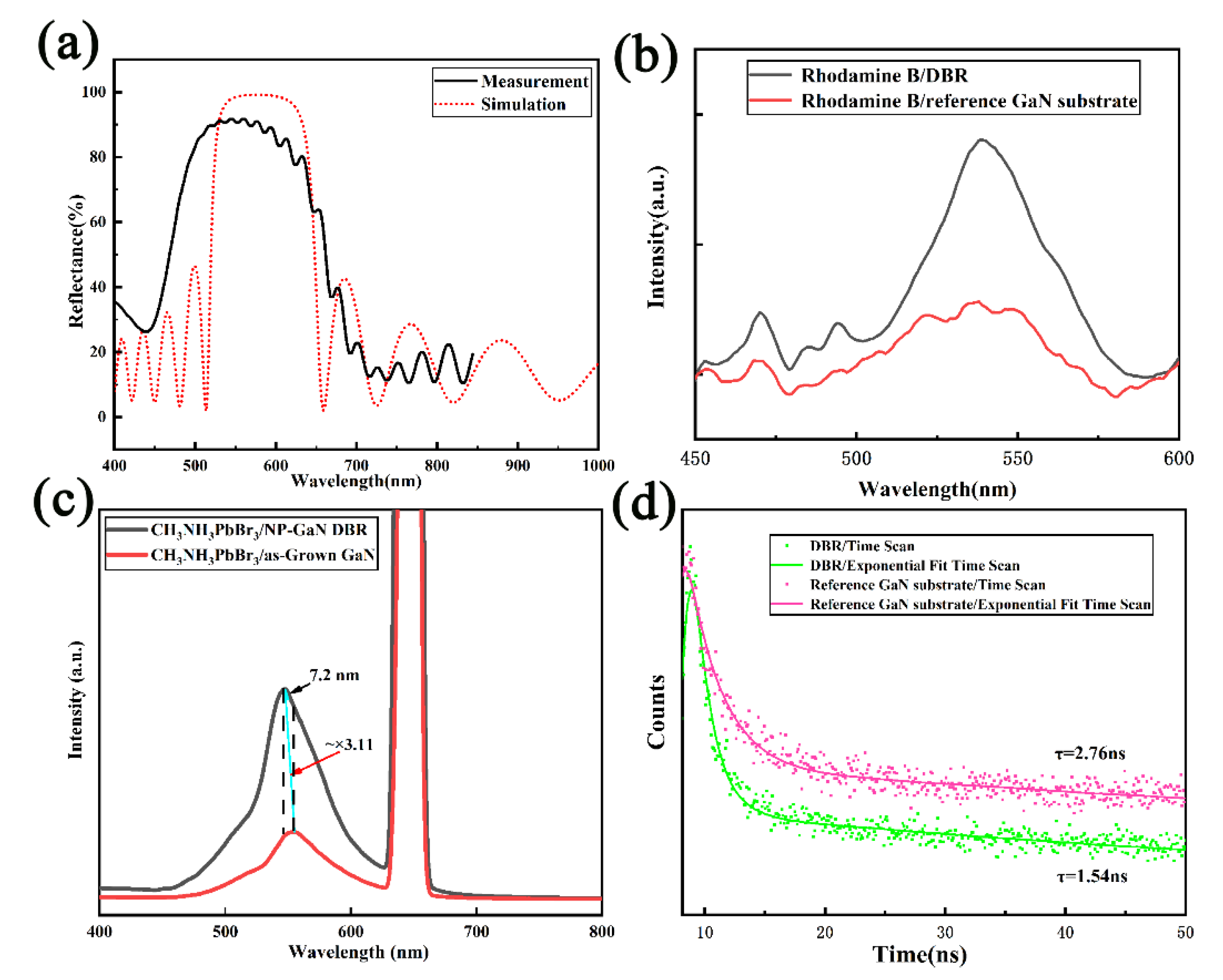
3. Results and Discussion

Figure 3a and b show the contact angles between the prepared DBR substrate and the saturated methanol solution of Pb(Ac)2 before and after the UV-O3 treatment. The surface of the prepared DBR substrate without treating by UV-O3 cannot form a good contact with the saturated methanol solution of Pb(Ac)2, as shown in Figure 3a. When the saturated methanol solution of Pb(Ac)2 contacts the untreated DBR substrate, it cannot spread out well, which makes it easy to accumulate on the DBR substrate. Therefore, it is difficult to form a uniform film after annealing treatment using a saturated methanol solution of Pb(Ac)2 on the untreated DBR substrate. The non-uniform Pb(Ac)2 film also does not react easily with the solution of CH3NH3Br/IPA uniformly. UV-O3 treatment of NP-GaN DBR substrate enhances the surface activity and affinity. UV-O3 treatment makes the contact angle reduce from 22° to 10°. After UV-O3 treatment, the saturated methanol solution of Pb(Ac)2 can rapidly spread on the substrate, which can be observed from Figure 3b. Figure 3c is the XRD patterns of the prepared DBR substrate before and after UV-O3 treatment. It can be seen that UV-O3 treatment does not break the chemical composition of the substrate, meaning that the UV-O3 treatment forms a physical adsorption of O3 on the surface of the substrate, enhancing surfactivity and moisturizing properties [40].
After UV-O3 treatment, a uniform Pb(Ac)2 film can be prepared on the DBR substrate, and the uniform Pb(Ac)2 film can react thoroughly with CH3NH3Br to form highly crystallized CH3NH3PbBr3 crystal. Figure 4a and b are the SEM images of CH3NH3PbBr3 crystals grown on the prepared DBR and reference substrates, respectively. As shown in the SEM images, the CH3NH3PbBr3 crystals on the prepared DBR and reference substrates are regular and large cubic particles with smooth surfaces and clear edges. During the formation of CH3NH3PbBr3 crystal, Pb(Ac)2 is slowly converted to CH3NH3PbBr3 through a two-step growth process. Firstly, the solid Pb(Ac)2 film reacts with Br ions in CH3NH3Br/IPA solution to form PbBr42− ions. Secondly, PbBr42− ions react with CH3NH3+ ions to form solid CH3NH3PbBr3 crystals. With the slow consumption of solid Pb(Ac)2 film, Pb precursor (PbBr42−) with a low concentration is combined with CH3NH3+ in the immersion solution to maintain the low supersaturated condition of CH3NH3PbBr3 crystal growth, which makes the CH3NH3PbBr3 crystal grow slowly and form a regular shape [16]. The CH3NH3PbBr3 crystal growth process can be shown using the following equation [16]:
PbAc2 (s) + 4Br (sol) → PbBr42− (sol) + 2Ac (sol)
PbBr42− (sol) + CH3NH3+ (sol) → CH3NH3PbBr3 (s) + Br (sol)
Figure 4c is the cross section of CH3NH3PbBr3 crystals prepared on prepared DBR substrate measured by SEM. Stacked CH3NH3PbBr3 crystals with clear edges can be observed from the cross-sectional SEM image; the periodic structure of the prepared DBR substrate can also be seen.
Figure 5a is the XRD spectra of the CH3NH3PbBr3 crystals grown on the prepared DBR and reference substrates. The firm peaks locate at 2θ = 15.2°, 21.4°, 30.4°, 37.5°, 43.3°, 46.1°and 62.8°, which are indexed to (100), (110), (200), (211), (220), (300) and (400) lattice planes of CH3NH3PbBr3 crystal [41,42,43], meaning that the prepared CH3NH3PbBr3 crystals belong to cubic space group Pm-3m [44]. The diffraction peaks of the (100) and (200) lattice planes are stronger than the others, indicating that the prepared CH3NH3PbBr3 crystals preferentially grow along (100) and (200) planes, and the other weaker diffraction peaks indicate that the prepared CH3NH3PbBr3 crystals are acceptable and perfect crystals [42,45]. The full width at half-maximum (FWHM) of (100) lattice plane is only 6 arcmin. The narrow FWHM and the straight baseline also state clearly that the prepared CH3NH3PbBr3 crystals have a good crystal quality. The peaks located at 18.5°, 25.5°, 30.4° which correspond to Pb(Ac)2 do not exist in the XRD patterns [16]. The reaction process continued for ~28 h. The long reaction time ensures that Pb(Ac)2 is transformed into CH3NH3PbBr3 completely, and there is no residue of Pb(Ac)2 in the prepared crystals. Compared with the XRD patterns of the prepared DBR substrate, the diffraction peaks locate at 2θ = 17.5°, 28.0°, 28.9°, 31.4°, 34.9°, 38.0°, 40.0°, 41.9°, 59.5° which are not marked in the XRD spectra and simultaneously present in the prepared DBR, CH3NH3PbBr3/NP-GaN DBR and CH3NH3PbBr3/reference substrate are the diffraction peaks of the GaN, sapphire substrate and the GaN epitaxial impurities. The two highest diffraction peaks, located at 34.9° and 41.9°, are indexed to GaN (0002) and c-surface sapphire (0006) of the substrate [46].
Figure 5b shows the FTIR spectra of CH3NH3PbBr3 crystals grown on the prepared DBR and reference substrates. The peak located at 910 cm−1 is regarded as the CH3-NH3+ rock (ν12) [47]. The peaks appearing at 1470, 1560, 3130 cm−1 can be accounted for by the NH3-related vibrations, which in order are related to the sym-NH3+ bend (ν3), asym-NH3+ bend (ν9) and sym-NH3+ stretch (ν1), respectively [47]. The peaks of the FTIR spectra are simultaneously present in the CH3NH3PbBr3 crystals grown on the prepared DBR and reference substrates. FTIR spectra indicate that CH3NH3PbBr3 crystals grown on the prepared DBR and reference substrates have the same structure.
When the scattering factor (χ = π d / λ , where d and λ   are pore diameter and wavelength of wave, respectively) of the nanoporous GaN layer is less than 0.2, the effective refractive index of nanoporous GaN layer can be obtained by the following formula [48]:
n p o r = ( 1 φ ) n 2 G a N + φ n 2 a i r
In the formula, φ stands for porosity of the nanoporous GaN layer, and npor, nGaN and nair stand for the effective refractive index of the nanoporous GaN layer, refractive index of GaN and refractive index of air, respectively. Based on the cross section of the prepared DBR substrate shown in Figure 1b, the porosity of the n-GaN layer is about 50%, and the porosity of the u-GaN layer is about 0%, while the refractive index of GaN at 550 nm is 2.40 and the one of air is 1. Therefore, according to the above formula, the refractive indexes of the doped layer and the undoped layer are calculated to be 1.83 and 2.40, respectively. The reflectance spectrum is simulated based on the above data. That is also the reason why the thicknesses of the n-GaN and u-GaN layers in the NP-GaN DBR are designed to be ~80 nm and ~60 nm, respectively, according to the formula that thickness is equal to λ/(4n). Figure 6a is the simulated and measured reflectance spectra of NP-GaN DBR. The simulated reflectance spectrum shows that the peak reflectivity is greater than 99%, and the stop band is from ~ 510 nm to ~ 655 nm. The experimental reflection spectrum shows that the reflectivity of the prepared DBR is about 92% at 550 nm and has a wider stop band (490–655 nm). The small differences between the experimental and simulated results are caused by the non-uniform EC etching process. In addition, the light interference signals in the reflectance spectrum can be seen, which could be attributed to the light reflected between the bottom GaN/NP-GaN DBR and top air/GaN interferences [39].
To verify the effect of the DBR substrate on PL intensity, rhodamine B thin layers with the same solution concentrations and the same thickness were spin-coated onto the DBR and reference substrates. Figure 6b is the PL spectra of rhodamine B spin-coated on the prepared DBR and reference substrates. The PL peaks of rhodamine B on the prepared DBR and reference substrates are all located at ~ 540 nm. The PL peak position of rhodamine B is consistent with the previously reported literature, which is located within the range of the stop band for the prepared DBR. It can be seen that the PL intensity of rhodamine B on the DBR substrate is ~3.2 times that of the film on the reference substrate. The enhancement of PL intensity is due to out-coupling of emission light in the film, according to previous literature [26,49].
Figure 6c is the PL spectra of CH3NH3PbBr3 crystals grown on the prepared DBR and reference substrates. The PL peak positions of CH3NH3PbBr3 crystals grown on the reference and prepared DBR substrate are located at 555.2 nm and 548 nm, respectively, similar to those of the cubic CH3NH3PbBr3 crystalline phase [42]. The PL intensity of CH3NH3PbBr3 crystals grown on the prepared DBR substrate shows a significant enhancement, approximately 3.11-fold, compared with that of CH3NH3PbBr3 crystals grown on the reference substrate. In order to exclude the effect of sample thickness, sample position, and local defects on the luminescence intensity, we collected the PL spectra of CH3NH3PbBr3 crystals grown on the DBR and reference substrates by changing the testing positions. The PL intensities of CH3NH3PbBr3 crystals grown on the prepared DBR substrate all show a significant enhancement, compared with that of CH3NH3PbBr3 crystals grown on the reference substrate. The photoluminescence enhancement is therefore not due to the sample thickness, sample position, or local defects. The PL intensity enhancement of CH3NH3PbBr3 crystals on a NP-GaN DBR substrate is caused by the out-coupling of emission light by constructive interference of reflected light at different interfaces of periodic NP-GaN layers [26,50,51]. Moreover, the PL peak of crystals on the prepared DBR substrate shows a ~7.2 nm blue-shift. The boundary effects and quantum size effects of quantum dots usually can have an effect on the peak position of the PL spectrum. The grain sizes of CH3NH3PbBr3 crystals grown on the DBR and reference substrates are almost the same and are in the order of microns, as shown in Figure 4. With such a large grain size, the boundary effect is almost absent. The blue shift of CH3NH3PbBr3 crystals grown on the DBR substrate is attributed to the stress relaxation [52,53]. According to the lattice constant of cubic CH3NH3PbBr3 and hexagonal GaN, the lattice mismatch between the CH3NH3PbBr3 and the NP-GaN DBR substrate is calculated to be ~7%. The CH3NH3PbBr3 crystals grown on the GaN substrates should have a considerable compressive stress. GaN film grown on sapphire substrate has high compressive stress, and it can be released due to the formation of a nanoporous GaN structure [54,55]. Therefore, the crystals grown on the prepared DBR substrate have lower stress compared with that on reference substrate. In addition, a very strong and narrow peak appears at 650 nm in the PL spectra of CH3NH3PbBr3 crystals grown on both the prepared DBR and reference substrate, which is an overtone related to the excitation laser of 325 nm. The wavelength of 650 nm is exactly twice that of the used laser.
Figure 6d shows the experimental and fitting PL decay profiles of CH3NH3PbBr3 crystals grown on the prepared DBR and reference substrates. The fitting short PL lifetime of CH3NH3PbBr3 crystals grown on the reference substrate is 2.76 ns, while the value of CH3NH3PbBr3 crystals grown on the DBR substrate is decreased to 1.54 ns. The relationship of the fluorescence quantum yield (ΦF), the rate constants for radiative (kr) and nonradiative (knr) deactivation, the fluorescence lifetime (τF) can be described by the following equation [56,57]:
Φ F = k r / k r + k n r = k r τ F
From this equation, we can see that the shorter τF corresponds to a larger kr, resulting in a bigger ΦF. This is consistent with the PL testing results in Figure 6c. According to previous literature, the spectral blue-shift of the PL spectrum is also associated with the shorter PL lifetime of CH3NH3PbBr3 crystals [58]. The enhancement of the PL intensity caused by the prepared DBR substrate demonstrates that NP-GaN DBR substrate can be used as an impactful platform for PL intensity enhancement of hybrid perovskite materials, and also provides a simple and effective new idea for the design and development of perovskite devices for large-area and broadband applications, e.g., CH3NH3PbX3-based lasers, photodetectors, light-emitting diodes and so on.

4. Conclusions

In summary, the EC etching method was used to fabricate nanoporous DBR. UV-O3 treatment of the substrate enhances the surfactivity of the NP-GaN DBR substrate. CH3NH3PbBr3 crystals were prepared on the UV-O3 treated nanoporous DBR substrate using a two-step immersion method. The SEM image shows that the CH3NH3PbBr3 crystals are regular, large cubic particles with smooth surfaces and clear edges. The XRD pattern indicates a good crystal quality of the CH3NH3PbBr3 crystals. The PL intensity of CH3NH3PbBr3 crystals grown on the nanoporous DBR substrate achieves a significant enhancement, compared with that on the reference substrate. This work provides an alternative way to develop or design optoelectronic devices based on hybrid perovskite materials. It may be used as an optical platform to obtain remarkable optical gain in hybrid perovskite-based devices, such as light-emitting diodes, lasers, photodetectors and multifunctional spintronic devices.

Author Contributions

Conceptualization, F.J.; Data curation, J.S. and Z.L.; Investigation, Y.D. and J.S.; Methodology, F.J. and J.S.; Writing—original draft, F.J.; Writing—review and editing, F.J. and Y.D. All authors have read and agreed to the published version of the manuscript.

Funding

This research was funded by the National Natural Science Foundation of China, grant number 11804043.

Data Availability Statement

The data presented in this study are available on request from the corresponding author.

Acknowledgments

The authors thank Liguo Gao for his support and advice.

Conflicts of Interest

The authors declare no conflict of interest.

References

  1. Huang, Y.X.; Tan, Q.S.; Fu, L.B.; Wang, X.G. Coherence dynamics of a two-mode Bose-Einstein condensate coupled with the environment. Phys. Rev. A 2013, 88, 063642. [Google Scholar] [CrossRef]
  2. Ki, W.; Li, J. A semiconductor bulk material that emits direct white light. J. Am. Chem. Soc. 2008, 130, 8114–8115. [Google Scholar] [CrossRef] [PubMed]
  3. Ki, W.; Li, J.; Eda, G.; Chhowalla, M. Direct white light emission from inorganic-organic hybrid semiconductor bulk materials. J. Mater. Chem. 2010, 20, 10676–10679. [Google Scholar] [CrossRef]
  4. Kojima, A.; Teshima, K.; Shirai, Y.; Miyasaka, T. Organometal halide perovskites as visible-light sensitizers for photovoltaic cells. J. Am. Chem. Soc. 2009, 131, 6050–6051. [Google Scholar] [CrossRef]
  5. Kim, H.S.; Lee, C.R.; Im, J.H.; Lee, K.B.; Moehl, T.; Marchioro, A.; Moon, S.J.; Humphry-Baker, R.; Yum, J.H.; Moser, J.E.; et al. Lead iodide perovskite sensitized all-solid-state submicron thin film mesoscopic solar cell with efficiency exceeding 9%. Sci. Rep. 2012, 2, 591. [Google Scholar] [CrossRef] [Green Version]
  6. Liu, M.Z.; Johnston, M.B.; Snaith, H.J. Efficient planar heterojunction perovskite solar cells by vapour deposition. Nature 2013, 501, 395–398. [Google Scholar] [CrossRef]
  7. He, Z.; Zhou, Y.; Liu, A.M.; Gao, L.G.; Zhang, C.; Wei, G.Y.; Ma, T.L. Recent progress in metal sulfide-based electron transport layers in perovskite solar cells. Nanoscale 2021, 13, 17272–17289. [Google Scholar] [CrossRef]
  8. Shoukat, F.; Kang, J.; Khan, Y.; Park, Y.; Lee, J.; Walker, B.; Seo, J. Solution-processed metal ion polyelectrolytes as hole transport materials for efficient inverted perovskite solar cells. Adv. Mater. Interfaces 2023, 2300043. [Google Scholar] [CrossRef]
  9. Stranks, S.D.; Eperon, G.E.; Grancini, G.; Menelaou, C.; Alcocer, M.J.P.; Leijtens, T.; Herz, L.M.; Petrozza, A.; Snaith, H.J. Electron-hole diffusion lengths exceeding 1 micrometer in an organometal trihalide perovskite absorber. Science 2013, 342, 341–344. [Google Scholar] [CrossRef] [Green Version]
  10. Cheng, Z.Y.; Lin, J. Layered organic-inorganic hybrid perovskites: Structure, optical properties, film preparation, patterning and templating engineering. Crystengcomm 2010, 12, 2646–2662. [Google Scholar] [CrossRef]
  11. Chen, J.N.; Zhou, S.S.; Jin, S.Y.; Li, H.Q.; Zhai, T.Y. Crystal organometal halide perovskites with promising optoelectronic applications. J. Mater. Chem. C 2016, 4, 11–27. [Google Scholar] [CrossRef]
  12. Rong, Y.G.; Mei, A.Y.; Liu, L.F.; Li, X.; Han, H.W. All-solid-state mesoscopic solar cells: From dye-sensitized to perovskite. ACTA Chim. Sin. 2015, 73, 237–251. [Google Scholar] [CrossRef] [Green Version]
  13. Rezaee, E.; Zhang, W.; Silva, S.R.P. Solvent engineering as a vehicle for high quality thin films of perovskites and their device fabrication. Small 2021, 17, 2008145. [Google Scholar] [CrossRef]
  14. Li, Y.W.; Meng, L.; Yang, Y.; Xu, G.Y.; Hong, Z.R.; Chen, Q.; You, J.B.; Li, G.; Yang, Y.; Li, Y.F. High-efficiency robust perovskite solar cells on ultrathin flexible substrates. Nat. Commun. 2016, 7, 10214. [Google Scholar] [CrossRef] [PubMed] [Green Version]
  15. Han, T.H.; Tan, S.; Xue, J.L.; Meng, L.; Lee, J.W.; Yang, Y. Interface and defect engineering for metal halide perovskite optoelectronic devices. Adv. Mater. 2019, 31, 1803515. [Google Scholar] [CrossRef]
  16. Zhu, H.M.; Fu, Y.P.; Meng, F.; Wu, X.X.; Gong, Z.Z.; Ding, Q.; Gustafsson, M.V.; Trinh, M.T.; Jin, S.; Zhu, X.Y. Lead halide perovskite nanowire lasers with low lasing thresholds and high quality factors. Nat. Mater. 2015, 14, 636–642. [Google Scholar] [CrossRef]
  17. Wong, A.B.; Lai, M.L.; Eaton, S.W.; Yu, Y.; Lin, E.; Dou, L.; Fu, A.; Yang, P.D. Growth and anion exchange conversion of CH3NH3PbX3 nanorod arrays for light-emitting diodes. Nano Lett. 2015, 15, 5519–5524. [Google Scholar] [CrossRef]
  18. Zhang, F.; Zhong, H.Z.; Chen, C.; Wu, X.G.; Hu, X.M.; Huang, H.L.; Han, J.B.; Zou, B.S.; Dong, Y.P. Brightly luminescent and color-tunable colloidal CH3NH3PbX3 (X = Br, I, Cl) quantum dots: Potential alternatives for display technology. ACS Nano 2015, 9, 4533–4542. [Google Scholar] [CrossRef]
  19. Levchuk, I.; Herre, P.; Brandl, M.; Osvet, A.; Hock, R.; Peukert, W.; Schweizer, P.; Spiecker, E.; Batentschuk, M.; Brabec, C.J. Ligand-assisted thickness tailoring of highly luminescent colloidal CH3NH3PbX3 (X = Br and I) perovskite nanoplatelets. Chem. Commun. 2017, 53, 244–247. [Google Scholar] [CrossRef]
  20. Yan, J.; Ke, X.H.; Chen, Y.L.; Zhang, A.; Zhang, B. Effect of modulating the molar ratio of organic to inorganic content on morphology, optical absorption and photoluminescence of perovskite CH3NH3PbBr3 films. Appl. Surf. Sci. 2015, 351, 1191–1196. [Google Scholar] [CrossRef]
  21. Yan, J.; Zhang, B.; Chen, Y.L.; Zhang, A.; Ke, X.H. Improving the photoluminescence properties of perovskite CH3NH3PbBr3,Cl-x films by modulating organic cation and chlorine concentrations. ACS Appl. Mater. Interfaces 2016, 8, 12756–12763. [Google Scholar] [CrossRef] [PubMed]
  22. Li, M.H.; Zhang, R.X.; Guo, Y.; Huan, Y.H.; Xi, J.H.; Li, Y.; Bai, Z.M.; Yan, X.Q. Introducing lead acetate into stoichiometric perovskite lewis acid-base precursor for improved solar cell photovoltaic performance. J. Alloys Compd. 2018, 767, 829–837. [Google Scholar] [CrossRef]
  23. Mosconi, E.; Azpiroz, J.; Angelis, F. Ab initio molecular dynamics simulations of methylammonium lead iodide perovskite degradation by water. Chem. Mater. 2015, 27, 4885–4892. [Google Scholar] [CrossRef]
  24. Sharma, R.; Choi, Y.S.; Wang, C.F.; David, A.; Weisbuch, C.; Nakamura, S.; Hu, E.L. Gallium-nitride-based microcavity light-emitting diodes with air-gap distributed Bragg reflectors. Appl. Phys. Lett. 2007, 91, 211108. [Google Scholar] [CrossRef]
  25. Sharma, R.; Haberer, E.D.; Meier, C.; Hu, E.L.; Nakamura, S. Vertically oriented GaN-based air-gap distributed Bragg reflector structure fabricated using band-gap-selective photoelectrochemical etching. Appl. Phys. Lett. 2005, 87, 051107. [Google Scholar] [CrossRef]
  26. Liu, J.; Liu, D.; Shen, Y.; Yang, X.; Zhao, C.; Chen, R.; Yang, Z.; Liu, J.; Ma, J.; Xiao, H. Fabrication and applications of wafer-scale nanoporous GaN near-infrared distributed Bragg reflectors. Opt. Mater. 2020, 107, 110093. [Google Scholar] [CrossRef]
  27. Wang, G.J.; Hong, B.S.; Chen, Y.Y.; Yang, Z.J.; Tsai, T.L.; Lin, Y.S.; Lin, C.F. GaN/AlGaN ultraviolet light-emitting diode with an embedded porous-AlGaN distributed Bragg reflector. Appl. Phys. Express 2017, 10, 122102. [Google Scholar] [CrossRef]
  28. Ng, H.M.; Doppalapudi, D.; Iliopoulos, E.; Moustakas, T.D. Distributed Bragg reflectors based on AlN/GaN multilayers. Appl. Phys. Lett. 1999, 74, 1036–1038. [Google Scholar] [CrossRef]
  29. Gacevic, Z.; Fernandez-Garrido, S.; Hosseini, D.; Estrade, S.; Peiro, F.; Calleja, E. InAlN/GaN Bragg reflectors grown by plasma-assisted molecular beam epitaxy. J. Appl. Phys. 2010, 108, 113117. [Google Scholar] [CrossRef]
  30. Ng, H.M.; Moustakas, T.D.; Chu, S.N.G. High reflectivity and broad bandwidth AlN/GaN distributed Bragg reflectors grown by molecular-beam epitaxy. Appl. Phys. Lett. 2000, 76, 2818–2820. [Google Scholar] [CrossRef]
  31. Chen, D.; Han, J. High reflectance memebrane-based distributed Bragg reflectors for GaN photonics. Appl. Phys. Lett. 2012, 101, 221104. [Google Scholar] [CrossRef]
  32. Mishkat-Ul-Masabih, S.; Luk, T.S.; Rishinaramangalam, A.; Monavarian, M.; Nami, M.; Feezell, D. Nanoporous distributed Bragg reflectors on free-standing nonpolar m-plane GaN. Appl. Phys. Lett. 2018, 112, 041109. [Google Scholar] [CrossRef]
  33. Carreno, J.M.; Passarelli, N.; Otero-Martinez, C.; Polavarapu, L.; Perez, L.A.; Reparaz, J.S.; Alonso, M.I.; Mihi, A. Enhanced Photoluminescence of Cesium Lead Halide Perovskites by Quasi-3D Photonic Crystals. Adv. Opt. Mater. 2022, 10, 2101324. [Google Scholar] [CrossRef]
  34. Chen, S.; Zhang, C.; Lee, J.; Han, J.; Nurmikko, A. High-Q, low-threshold monolithic perovskite thin-film vertical-cavity lasers. Adv. Mater. 2017, 29, 1604781. [Google Scholar] [CrossRef] [PubMed]
  35. Liu, Q.; Yang, Y.; Wang, X.; Song, W.; Luo, X.; Guo, J.; Shi, J.; Cheng, C.; Li, D.; He, L.; et al. High-performance UV–visible photodetectors based on CH3NH3PbI3-xClx/GaN microwire array heterostructures. J. Alloys Compd. 2021, 864, 158710. [Google Scholar] [CrossRef]
  36. Yang, Y.; Lin, Y.; Xiang, P.; Liu, M.; Chen, W.; Han, X.; Hu, G.; Hu, G.; Zang, W.; Lin, X.; et al. Vertical-conducting InGaN/GaN multiple quantum wells LEDs with AlN/GaN distributed Bragg reflectors on Si(111) substrate. Appl. Phys. Express 2014, 7, 042102. [Google Scholar] [CrossRef]
  37. Zambrano-Serrano, M.A.; Hernandez, C.A.; de Melo, O.; Behar, M.; Gallardo-Hernandez, S.; Casallas-Moreno, Y.L.; Ponce, A.; Hernandez-Robles, A.; Bahena-Uribe, D.; Yee-Rendon, C.M.; et al. Effects of heavy Si doping on the structural and optical properties of n-GaN/AlN/Si(111) heterostructures. Mater. Res. Express 2022, 9, 065903. [Google Scholar] [CrossRef]
  38. Ni, Y.Q.; He, Z.Y.; Yang, F.; Zhou, D.Q.; Yao, Y.; Zhou, G.L.; Shen, Z.; Zhong, J.; Zhen, Y.; Wu, Z.S. Effect of AlN/GaN superlattice buffer on the strain state in GaN-on-Si(111) system. Jpn. J. Appl. Phys. 2015, 54, 015505. [Google Scholar] [CrossRef]
  39. Cao, D.Z.; Yang, X.K.; Shen, L.Y.; Zhao, C.C.; Luan, C.N.; Ma, J.; Xiao, H.D. Fabrication and properties of high quality InGaN-based LEDs with highly reflective nanoporous GaN mirrors. Photonics Res. 2018, 6, 1144–1150. [Google Scholar] [CrossRef]
  40. Lim, K.T.P.; Deakin, C.; Ding, B.N.; Bai, X.Y.; Griffin, P.; Zhu, T.T.; Oliver, R.A.; Credgington, D. Encapsulation of methylammonium lead bromide perovskite in nanoporous GaN. APL Mater. 2019, 7, 021107. [Google Scholar] [CrossRef] [Green Version]
  41. Huang, H.; Susha, A.S.; Kershaw, S.V.; Hung, T.F.; Rogach, A.L. Control of emission color of high quantum yield CH3NH3PbBr3 perovskite quantum dots by precipitation temperature. Adv. Sci. 2015, 2, 1500194. [Google Scholar] [CrossRef] [PubMed]
  42. Han, L.P.; Liu, C.; Wu, L.L.; Zhang, J.Q. Observation of the growth of MAPbBr(3) single-crystalline thin film based on space-limited method. J. Cryst. Growth 2018, 501, 27–33. [Google Scholar] [CrossRef]
  43. Ghosh, S.; Rana, D.; Pradhan, B.; Donfack, P.; Hofkens, J.; Materny, A. Vibrational study of lead bromide perovskite materials with variable cations based on Raman spectroscopy and density functional theory. J. Raman Spectrosc. 2021, 52, 2338. [Google Scholar] [CrossRef]
  44. Tang, Y.; Yan, N.; Wang, Z.W.; Yuan, H.D.; Xin, Y.L.; Yin, H.F. Precursor solution volume-dependent ligand-assisted synthesis of CH3NH3PbBr3 perovskite nanocrystals. J. Alloys Compd. 2019, 773, 227–233. [Google Scholar] [CrossRef]
  45. Li, X.J.; Wang, K.Y.; Chen, M.M.; Wang, S.S.; Fan, Y.B.; Liang, T.; Song, Q.H.; Xing, G.C.; Tang, Z.K. Stable whispering gallery mode lasing from solution-processed formamidinium lead bromide perovskite microdisks. Adv. Opt. Mater. 2020, 8, 2000030. [Google Scholar] [CrossRef]
  46. Xin, Y.; Gao, Z.; Shang, X.; Wu, J.; Yu, D.; Xiu, J.; Li, Z. Effect of thermal annealing on the structural and optical properties of ZnGa2O4 films deposited on sapphire by magnetron sputtering. J. Alloys Compd. 2023, 933, 167760. [Google Scholar] [CrossRef]
  47. Yu, W.; Jiang, Y.; Zhu, X.; Luo, C.; Jiang, K.; Chen, L.; Zhang, J. Diversity of band gap and photoluminescence properties of lead halide perovskite: A halogen-dependent spectroscopic study. Chem. Phys. Lett. 2018, 699, 93. [Google Scholar] [CrossRef]
  48. Braun, M.M.; Pilon, L. Effective optical properties of non-absorbing nanoporous thin films. Thin Solid Films 2006, 496, 505–514. [Google Scholar] [CrossRef]
  49. Liu, J.; Yang, X.; Zhao, C.; Chen, R.; Luan, C.; Xiao, H. Eu-doped Lu2O3 epitaxial films with an embedded nanoporous GaN distributed Bragg reflectors. Ceram. Int. 2021, 47, 22693. [Google Scholar] [CrossRef]
  50. Chen, Y.C.; Yeh, H.; Lee, C.J.; Chang, W.H. Distributed Bragg reflectors as broadband and large-area platforms for light-coupling enhancement in 2D transition-metal dichalcogenides. ACS Appl. Mater. Interfaces 2018, 10, 16874–16880. [Google Scholar] [CrossRef]
  51. Lien, D.H.; Kang, J.S.; Amani, M.; Chen, K.; Tosun, M.; Wang, H.P.; Roy, T.; Eggleston, M.S.; Wu, M.C.; Dubey, M.; et al. Engineering light outcoupling in 2D materials. Nano Lett. 2015, 15, 1356–1361. [Google Scholar] [CrossRef]
  52. Wang, W.J.; Yang, G.F.; Chen, P.; Yu, Z.G.; Liu, B.; Xie, Z.L.; Xiu, X.Q.; Wu, Z.L.; Xu, F.; Xu, Z.; et al. Characteristics of nanoporous InGaN/GaN multiple quantum wells. Superlattices Microst. 2014, 71, 38–45. [Google Scholar] [CrossRef]
  53. Wang, Q.; Zhu, C.R.; Zhou, Y.F.; Wang, X.S.; Liu, B.L.; Wang, X.L.; Lv, Y.J.; Feng, Z.H.; Xu, X.G.; Ji, Z.W. Fabrication and photoluminescence of strong phase-separated InGaN based nanopillar LEDs. Superlattices Microst. 2015, 88, 323–329. [Google Scholar] [CrossRef]
  54. Chen, R.; Wang, D.; Liu, J.; Feng, B.; Zhu, H.; Han, X.; Luan, C.; Ma, J.; Xiao, H. Ta-Doped Ga2O3 Epitaxial Films on Porous p-GaN Substrates: Structure and Self-Powered Solar-Blind Photodetectors. Cryst. Growth Des. 2022, 22, 5285–5292. [Google Scholar] [CrossRef]
  55. Cao, D.Z.; Xiao, H.D.; Gao, Q.X.; Yang, X.K.; Luan, C.N.; Mao, H.Z.; Liu, J.Q.; Liu, X.D. Fabrication and improved photoelectrochemical properties of a transferred GaN-based thin film with InGaN/GaN layers. Nanoscale 2019, 9, 11504–11510. [Google Scholar] [CrossRef]
  56. Chouhan, L.; Ito, S.; Thomas, E.M.; Takano, Y.; Ghimire, S.; Miyasaka, H.; Biju, V. Real-time blinking suppression of perovskite quantum dots by halide vacancy filling. ACS Nano 2021, 15, 2831. [Google Scholar] [CrossRef]
  57. Park, S.; Kwon, J.; Park, S.; Kwon, O.; Kim, J.; Yoon, S.; Chung, J.; Whang, D.; Park, S.; Lee, D.; et al. Grystallization-induced emission enhancement and amplified spontaneous emission from a CF3-containing excited-state intramolecular-proton-transfer molecule. Adv. Opt. Mater. 2017, 5, 1700353. [Google Scholar] [CrossRef]
  58. Zhang, Z.; Ghimire, S.; Okamoto, T.; Sachith, B.M.; Sobhanan, J.; Subrahmanyam, C.; Biju, V. Mechano-optical modulation of excitons and carrier recombination in self-assembled halide perovskite quantum dots. ACS Nano 2022, 16, 160. [Google Scholar] [CrossRef]
Figure 1. (a) The diagrammatic sketch of etching process at room temperature; (b) The cross section of NP-GaN DBR by SEM; (c) The high-resolution SEM cross section of NP-GaN DBR.
Energies 16 04547 g001
Figure 2. Preparation process diagram of CH3NH3PbBr3 crystals.
Energies 16 04547 g002
Figure 3. The contact angles between the prepared DBR substrate and the saturated methanol solution of Pb(Ac)2 (a) before and (b) after the UV-O3 treatment; (c) The XRD patterns of the prepared DBR substrate before and after the UV-O3 treatment.
Energies 16 04547 g003
Figure 4. The SEM image of CH3NH3PbBr3 crystals grown on (a) prepared DBR and (b) reference substrates; (c) The cross section of CH3NH3PbBr3 crystals grown on DBR substrates measured by SEM.
Energies 16 04547 g004
Figure 5. (a) The XRD spectra of the CH3NH3PbBr3 crystals grown on the NP-GaN DBR and reference unetched GaN substrates; (b) FTIR spectra of the CH3NH3PbBr3 crystals grown on the NP-GaN DBR and reference unetched GaN substrates.
Energies 16 04547 g005
Figure 6. (a) The simulated and measured reflectance spectra of NP-GaN DBR; (b) The PL spectra of rhodamine B spin-coated on the prepared DBR and reference substrate; (c) The PL spectra of CH3NH3PbBr3 crystals grown on the prepared DBR and reference substrates; (d) PL decay profiles of CH3NH3PbBr3 crystals grown on the prepared DBR and reference substrates.
Energies 16 04547 g006
Disclaimer/Publisher’s Note: The statements, opinions and data contained in all publications are solely those of the individual author(s) and contributor(s) and not of MDPI and/or the editor(s). MDPI and/or the editor(s) disclaim responsibility for any injury to people or property resulting from any ideas, methods, instructions or products referred to in the content.

