Article

Compensation-Voltage-Injection-Based Neutral-Point Voltage Fluctuation Suppression Method for NPC Converters †

1
School of Electronic Information and Electrical Engineering, Shanghai Jiao Tong University, Shanghai 200240, China
2
Collage of Electrical Engineering, Shanghai University of Electric Power, Shanghai 200090, China
3
Shanghai Xilong Technology Co., Ltd., Shanghai 201109, China
4
Shanghai Chint Power Systems Co., Ltd., Shanghai 201614, China
*
Author to whom correspondence should be addressed.
This paper is an extended version of our paper published in 2022 Asia Power and Electrical Technology Conference (APET), Shanghai, China, 11–13 November 2022.
Energies 2023, 16(11), 4409; https://doi.org/10.3390/en16114409
Submission received: 8 March 2023 / Revised: 19 May 2023 / Accepted: 25 May 2023 / Published: 30 May 2023

Abstract

:
Three-level neutral-point clamped (NPC) inverters are widely used in the new energy power generation, motor drive, and many other occasions. However, the neutral-point voltage imbalance of an NPC inverter will affect the output of the inverter system, and the control of the neutral point voltage has become a popular research topic. In this paper, a compensation-voltage-injection-based neutral-point voltage balancing method is proposed. During the switching cycle, the average value model of the neutral-point current under different voltage vectors is applied to calculate the value of the compensation voltage that needs to be injected. The self-balance of the neutral-point voltage based on a switching cycle is realized, and the influence of modulation ratio and power factor on equalization ability is discussed. A MATLAB/Simulink simulation model and a small power prototype are established to verify the effectiveness of the method, and the simulation and experimental results show that the proposed method can effectively suppress the neutral-point voltage fluctuation in a wide range of modulation ratios and power factors.

1. Introduction

Compared with the two-level inverter, the three-level neutral-point-clamped (NPC) [1,2] inverter has the advantages of less switching stress and less harmonic content of output voltage. It is widely used in the new energy power generation, active power filter (APF), flexible AC transmission system (FACTS), motor drive, and other medium high-voltage, high-power occasions.
However, there is a key technical problem in this topology, which is the balance of the neutral-point voltage [3]. This topology requires two capacitors in series on the DC side to output three levels of phase voltage on the AC side. Under ideal conditions, the voltage of each capacitor is half the voltage of the DC bus. However, there will be current flowing out of the neutral point, causing voltage fluctuation. The unbalance of neutral-point voltage results in low-frequency harmonics in the output voltage, which reduces the waveform quality of the output voltage. At the same time, the voltage stress of the power switching device is inconsistent, which may damage the switching device and affect the normal operation of the system [4]. Therefore, capacitor voltage balance control becomes one of the key points in the research of three-level NPC inverters.
To solve this problem, many hardware methods such as increasing the capacitance value or replacing the capacitor with a DC source can effectively reduce or even eliminate the fluctuation of the neutral-point voltage. This problem can also be ameliorated by modifying the modulation strategy, which greatly reduces the cost and volume of the system compared with the hardware methods. Many scholars have studied the balance control of capacitor voltage in NPC inverters. The proposed balance control method can be summarized as a space vector pulse width modulation (SVPWM) method and a carrier-based pulse width modulation (CBPWM) method [5,6,7]. The former usually adopts the method of adjusting the action time of a pair of redundant small vectors to adjust the neutral-point voltage under the condition of keeping the output line voltage unchanged [8,9], while the latter mostly adopts the method of injecting compensation voltage to realize the balance of capacitor voltage [10,11,12].
Refs. [13,14] proposed a hybrid modulation technique of virtual SVPWM and SVPWM. SVPWM is used when the neutral-point voltage is balanced; otherwise, virtual SVPWM is used. However, under the conditions of high-modulation ratio and low-power factor, the proportion of virtual SVPWM exceeds 80%. The switching loss of virtual SVPWM is much larger than that of CBPWM or SVPWM, so virtual SVPWM can balance the midpoint voltage, but it will bring huge switching losses.
Refs. [15,16] proposed proportional integral (PI)-based regulation. The control method of the capacitor can suppress the DC voltage deviation and reduce the low-frequency fluctuation through PI parameter matching, but the instantaneous control effect of voltage balancing regulation is weakened when the load changes. According to the SVPWM principle of nearest three vector (NTV), a CBPWM voltage balancing control strategy with zero-sequence component injection is proposed in [17]. This method can reduce the switching loss and reduce the low-frequency oscillation of neutral-point voltage in a certain range of working conditions, but it sacrifices the quality of AC output waveform.
Ref. [18] proposed an algebraic modulation strategy using a math model to transform the gate signal into a general modulation matrix solution with three free parameters. By designing free parameters and arranging switching patterns, the neutral-point voltage is achieved without any other controllers. Ref. [19] used low common-mode voltage vectors to generate a PWM signal. The neutral-point current was controlled by selecting limited vectors and modulation mode. The leakage current was suppressed during the balancing process.
In [20], a harmonic voltage-injection-based DC-Link imbalance compensation technique method was proposed. The offset voltage consisted of double the frequency harmonic and the voltage difference of the two DC capacitors. Ref. [21] found that the amplitude of neutral-point voltage fluctuation was a function of load current amplitude, power angle, and modulation ratio. In [22], an offset voltage injection based on a modified min–max function was proposed. The min–max function limited the modulation ratio, and a further adjustable voltage signal of the difference of capacitor voltage was added to balance the neutral-point voltage.
In this paper, a compensation voltage injection method in a switching cycle based on CBPWM is proposed. By analyzing the neutral-point current under different voltage vectors, an average model of neutral-point current and voltage fluctuation is built to estimate the relationship between the voltage fluctuation and the load current, and the expected compensation voltage is calculated to minimize the fluctuation. Compared to the method of adjusting the voltage vectors to suppress the fluctuation, the compensation voltage injection based on the switching cycle method has a better suppression extent and a faster response. The influence of modulation ratio and power factor is analyzed, and the voltage can be self-equalized within a switching cycle in a wide range of modulation ratios and power factors. The simulation model on MATLAB/Simulink and a small power prototype are established to verify the effectiveness of the proposed method.

2. Analysis and Modeling of Neutral-Point Voltage Fluctuation

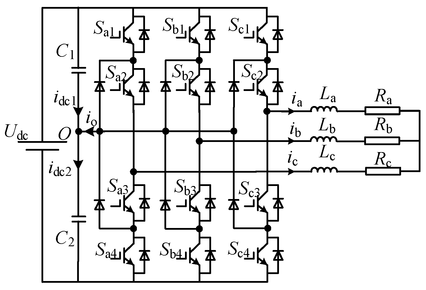
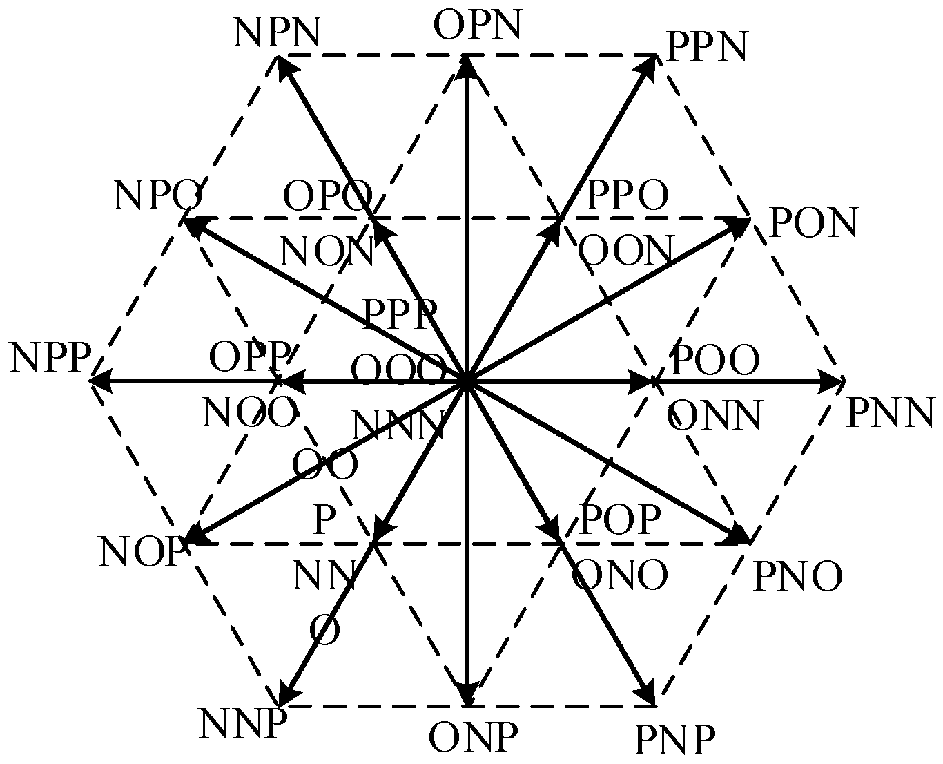
2.1. Principle of Modulation Strategy for NPC Inverter

Figure 1 shows the topology of a three-phase, three-level NPC inverter, with each phase arm consisting of four switching tubes and two clamped diodes. C 1 and C 2 are bus capacitors, and U d c is the DC source voltage. The switching variable S a , S b , and S c are defined as the bridge arm output level state of phase a, b, and c. Table 1 shows the corresponding relationship between the output voltage u a o and the switching state variable S a .
The output level state of a three-phase three-level inverter is a combination of S a , S b , and S c , so there are 27 kinds of switching status, known as 27 voltage vectors. Figure 2 shows the corresponding relationships of 27 space vectors in the vector diagram.
Under different voltage vectors, the NPC circuit topology is different due to the influence of voltage on the neutral point. The 27 voltage vectors in Figure 2 are generally divided into four categories. A typical example of how voltage vectors influence the neutral-point current is shown in Figure 3 in each category.
Based on Figure 2 and Figure 3, 6 of 27 vectors are large vectors (PPN, PNN, PNP, NPP, NPN, NNP), which have no influence on the neutral-point voltage; 3 of 27 vectors are zero vectors (PPP, OOO, NNN), which will also cause no current to flow in or flow out from the neutral point; and 12 small vectors (POO PPO…) and 6 medium vectors (PON, OPN…) will cause current to flow into or out from the neutral point, thus causing the voltage fluctuation. According to the reference direction of neutral-point current i o and load current i a , i b , and i c shown in Figure 3, the relationship between i o and i a , i b , i c under switching status of medium vectors and small vectors is shown in Table 2.

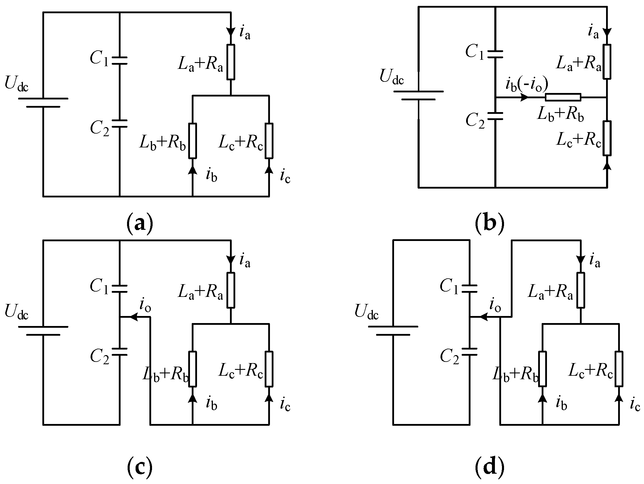
2.2. Modeling of Neutral-Point Voltage Fluctuation

As shown in Figure 1, according to the circuit principle we have the formula:
i dc 1 = C 1 d u dc 1 d t i dc 2 = C 2 d u dc 2 d t i o = i dc 2 i dc 1 Δ U = u dc 1 u dc 2 2 d u dc 1 + d u dc 2 = 0
Assuming that C 1 = C 2 = C , we thus acquire the voltage fluctuation of the neutral point:
Δ U = 1 2 i o d t C
According to (2), the fluctuation of the neutral-point voltage is related to the direction and value of i o . During a switching period, the switching status is usually a process of vectors changing among large vectors, medium vectors, and small vectors. As can be seen from Table 2, i o depends on the switching state and the magnitude and direction of the load current. To analyze the switching states, firstly, suppose a set of modulation signals are given as (3) and ideal current output as (4):
u a = m cos ( ω t ) u b = m cos ( ω t 2 3 π ) u c = m cos ( ω t + 2 3 π )
i a = I cos ( ω t φ ) i b = I cos ( ω t 2 3 π φ ) i c = I cos ( ω t + 2 3 π φ )
where m is the modulation ratio, I is the amplitude of the output current, and φ is the power angle. Under the modulation wave of (3), the generation process and the neutral-point current of a certain period is shown in Figure 4.
From Figure 4, it can be seen that there are 4 states (OOO, OON, PON, PNP) during this switching cycle under CBPWM. For each switching period, d a , d b , d c respectively represent the time when S a , S b , S c are not equal to 0. For the switching status of OON, i o = i c , and the duration is d c d a ; for the switching status of PON, i o = i b , and the duration is d a d b ; for the switching status of OOO and PPN, i o = 0, and the duration is 1 d c + d b . So, we can obtain the neutral-point fluctuation based on (2) during this switching period:
Δ U = 1 2 C ( d c d a i a d t + d a d b i b d t + 1 d c + d b 0 d t )
Suppose that the switching cycle is relatively short enough; thus, there is very little change of reference signal and load current during one switching cycle, and it can be assumed that both remain constant during one switching cycle. Thus, the following assumptions can be made:
u a = u a T s T s u a d t = u a T s T s = u a T s d a = u a = u a s i g n ( u a )
where u a T s means the average value of u a during a switching period of T s , s i g n ( u a ) means the positivity or negativity of u a . According to Figure 4, the voltage variation can be calculated:
Δ U = 1 2 C [ ( d a d c ) T s i a + ( d c d b ) T s ( i b ) ]
Combining (6) and (7), the voltage variation can be replace with:
Δ U = 1 2 C T s u a i a s i g n ( u a ) + u b i b s i g n ( u b ) + u c i c s i g n ( u c ) d t
More generally, it can be found that (8) not only applies to the switching state in Figure 4, but also to every switching period based on CBPWM modulation.
Figure 5 is a simple simulation verification for (8) during a power frequency cycle. It can be seen that there are only very few discretization errors in each switching cycle.

3. Proposed Voltage Fluctuation Suppression Method

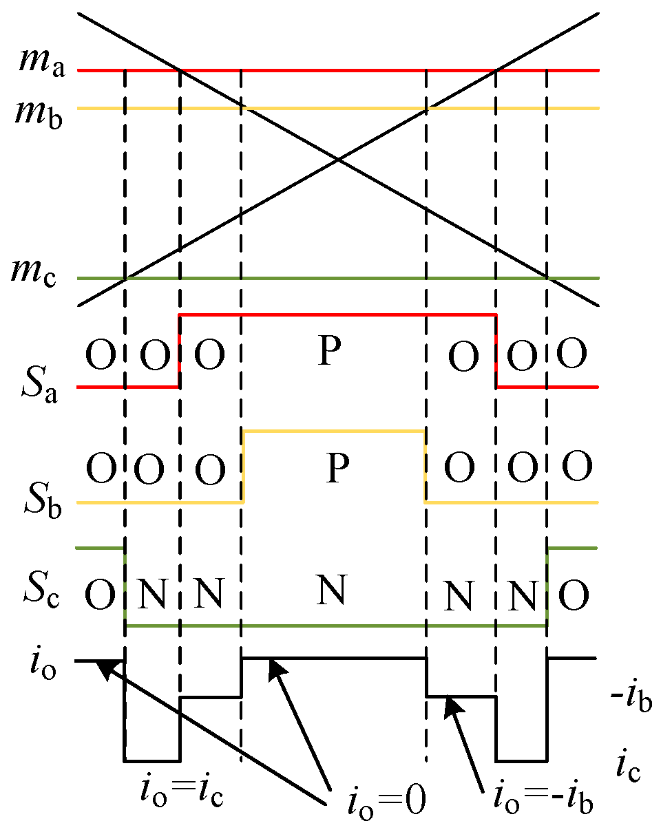
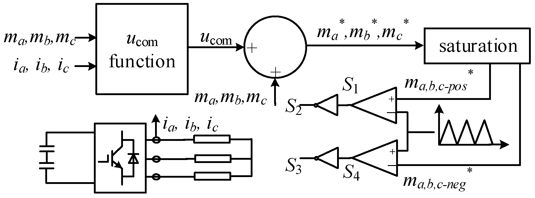
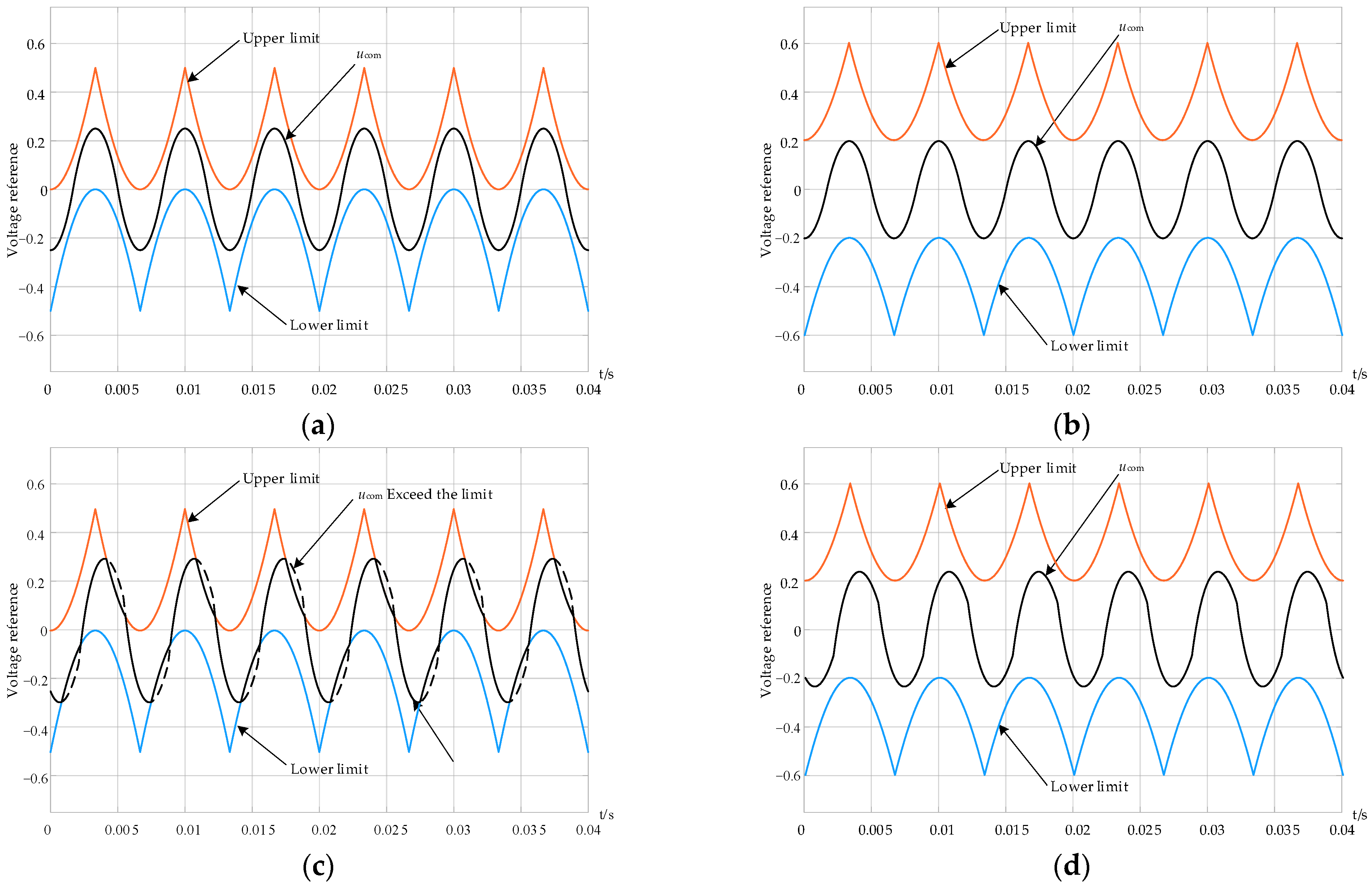
3.1. Switching-Cycle-Based Compensation Voltage Injection Method

From (8), we can see that during one switching cycle, the voltage variation is the function of voltage reference and load current. If a compensation signal u c o m is injected into the three-phase reference voltage, then the voltage variation during one switching cycle will be:
Δ U = 1 2 C T s ( u a + u com ) i a s i g n ( u a + u com ) + ( u b + u com ) i b s i g n ( u b + u com ) + ( u c + u com ) i c s i g n ( u c + u com ) d t
To minimize the neutral-point voltage fluctuation, one effective method is to minimize voltage variation within each switching cycle, which means minimizing the absolute value of Δ U . Considering Δ U = 0 , we can solve (9) and obtain:
u com = A B A = u a i a s i g n ( u a + u com ) + u b i b s i g n ( u b + u com ) + u c i c s i g n ( u c + u com ) B = i a s i g n ( u a + u com ) + i b s i g n ( u b + u com ) + i c s i g n ( u c + u com )
As for (9), the key to solving this equation is whether the value of sign function changes after adding u c o m to u a b c . In general, the case of sign function change after u c o m is added to u a b c occurs on the signal which is closest to 0. Therefore, to solve (10), firstly, suppose the value of “sign” function does not change after compensation of u c o m , thus, (10) can be solved as in (11):
u com = A B A = u a i a s i g n ( u a ) + u b i b s i g n ( u b ) + u c i c s i g n ( u c ) B = i a s i g n ( u a ) + i b s i g n ( u b ) + i c s i g n ( u c )
Then, sort u a , u b , and u c as u m i n , u m i d , and u m a x . Substitute the value of u c o m into s i g n ( u m i d + u c o m ) to check whether it changes after compensation. If not, then the value of u c o m is the correct compensation voltage signal need to inject into the reference signal. If the value of sign function has changed, then s i g n ( u m i d + u c o m ) = s i g n ( u m i d ) , map u m i d to u a b c and resolve it using (10).
Since the signal u a , u b , u c , and u c o m are the modulation reference signals, then we have the limitations for u c o m in (12):
1 u a + u com 1 1 u b + u com 1 1 u c + u com 1
Therefore, the process of solving the compensation voltage is a process of “Assumption—Verification—Correction—Limitation”.
Assumption: assume that the sign function does not change after compensation and solve the compensation voltage using (11).
Verification: sort u a , u b , and u c . Check whether s i g n ( u m i d + u c o m ) satisfies the assumption that it does not change after compensation.
Correction: if it satisfies, skip this step. If not, correct the value s i g n ( u m i d + u c o m ) = s i g n ( u m i d ) and recalculate the compensation voltage using (10).
Limitation: check that the compensation voltage does not exceed the limit in (12). If so, correct it to the maximum or minimum limit.
Figure 6 shows the control block diagram of the proposed method. The sampled three-phase current signal and the original modulation signal are the input to the u c o m calculation function. Through (10) to (12) and the above process, the compensated voltage is obtained. The compensated voltage is injected into the modulation wave signal m a b c . The mabc* is the modulation signal after injection and the gate signal of the switch is obtained after amplitude limiting and comparison with the triangular carrier.

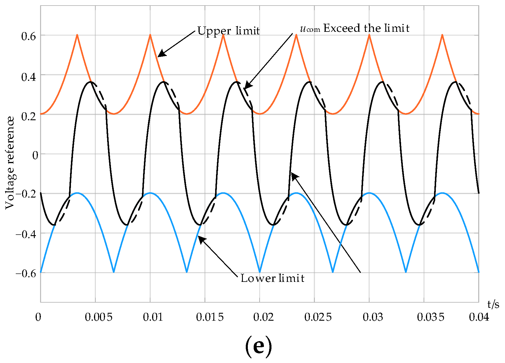
3.2. Influence of Modulation Rate and Power Factor

Based on the analysis in Section 3.1, the neutral-point voltage can be self-balanced by making the voltage variation Δ U = 0 within each switching cycle. At the same time, since the time scale of balance is the switching period, even if the value of busbar capacitor C 1 and C 2 is very small, the voltage variation Δ U caused by the neutral-point current will be still very low according to (2).
However, it is not always possible for the voltage variation Δ U = 0 . The value of u c o m is greatly affected by the modulation ratio m and the power factor c o s ( φ ) . As it is affected by the amplitude limit shown in (12), when u c o m exceeds the limit, the voltage variation Δ U is no longer equal to 0, and so there will be much larger voltage fluctuation.
Figure 7 shows the compensation voltage calculated using the proposed method under different modulation ratios and power angles. By contrasting (a) with (b), it can be seen that the compensation voltage will not exceed the limit even if the modulation ratio m is 1 when cos φ = 1 . When the modulation ratio m is reduced to 0.8, the compensation voltage has a looser limit. Therefore, the proposed method is more suitable for the situation of a lower modulation ratio m. The lower the modulation ratio, the more likely the voltage variation Δ U is to be 0 in the switching cycle.
By contrasting (a) with (c), when the power angle φ changes to π / 6 , the condition voltage variation Δ U = 0 can no longer be satisfied because the voltage to be compensated exceeds the limit of the modulating wave. Therefore, the proposed method is more suitable for the situation of a larger value of power factor cos φ . The closer | cos φ | is to 1, the more likely the voltage variation Δ U is to be 0 in the switching cycle.
In Figure 7d, although the power angle is still π / 6 , the condition voltage variation Δ U = 0 can still be satisfied because of the reduction in the modulation ratio m. However, with the further change of the power factor cos φ , the compensation voltage still exceeds the limit under the lower modulation ratio m, so the voltage variation Δ U = 0 in the switching cycle cannot be satisfied at this time, and there will be voltage fluctuation at the neutral point. However, the fluctuation amplitude is still much smaller than that without voltage compensation, because the voltage variation Δ U during the switching cycle has been limited to the minimum.

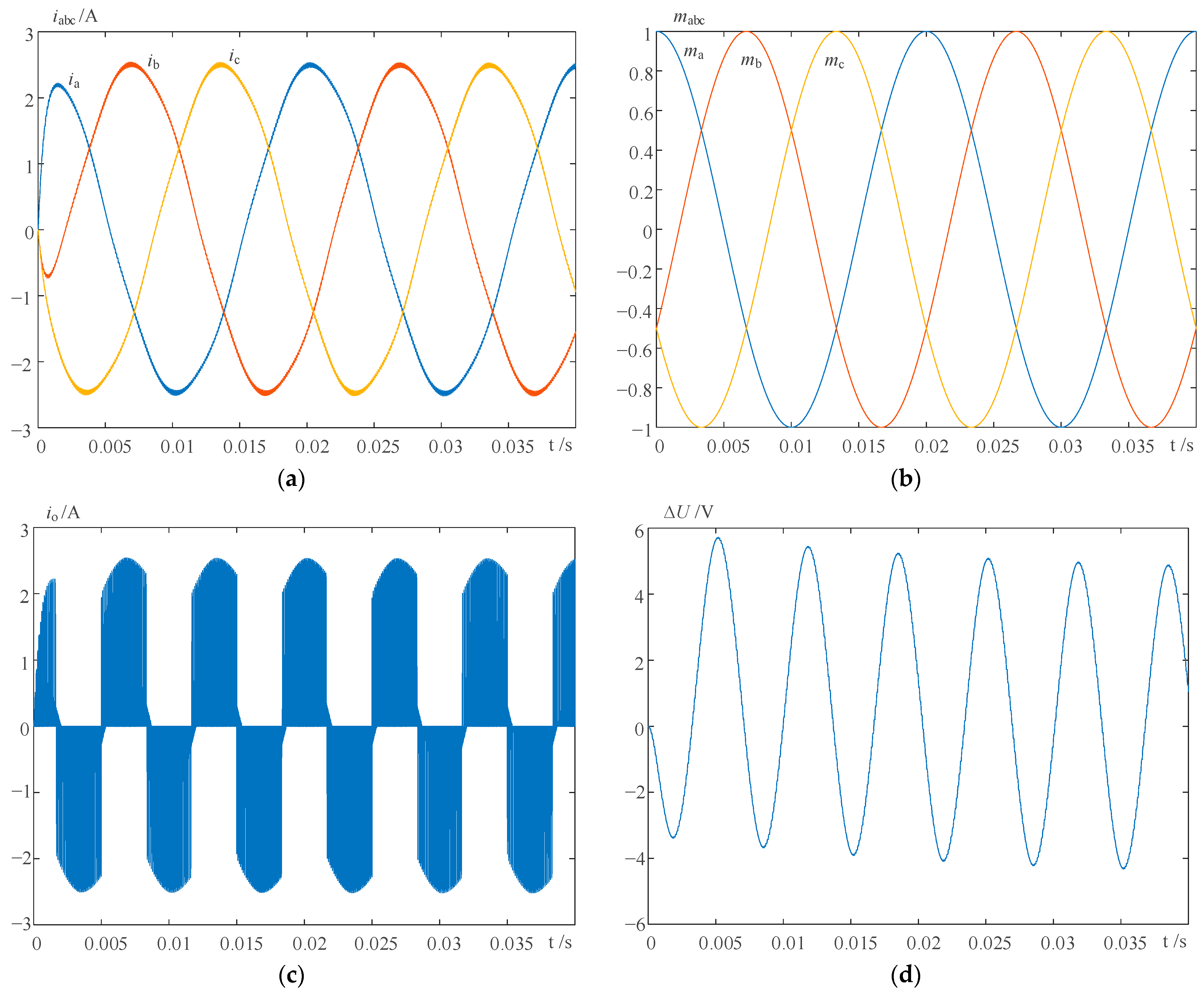
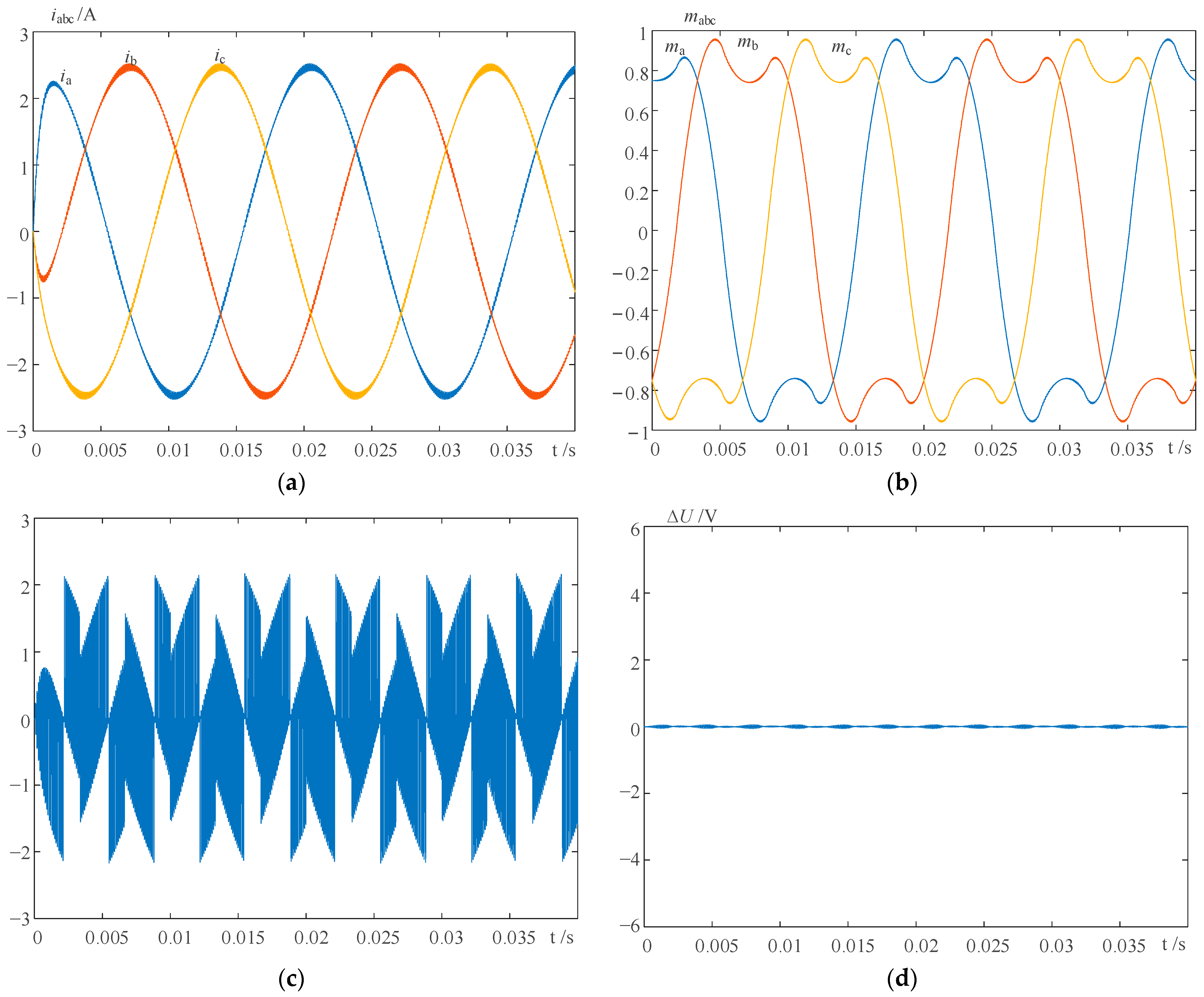
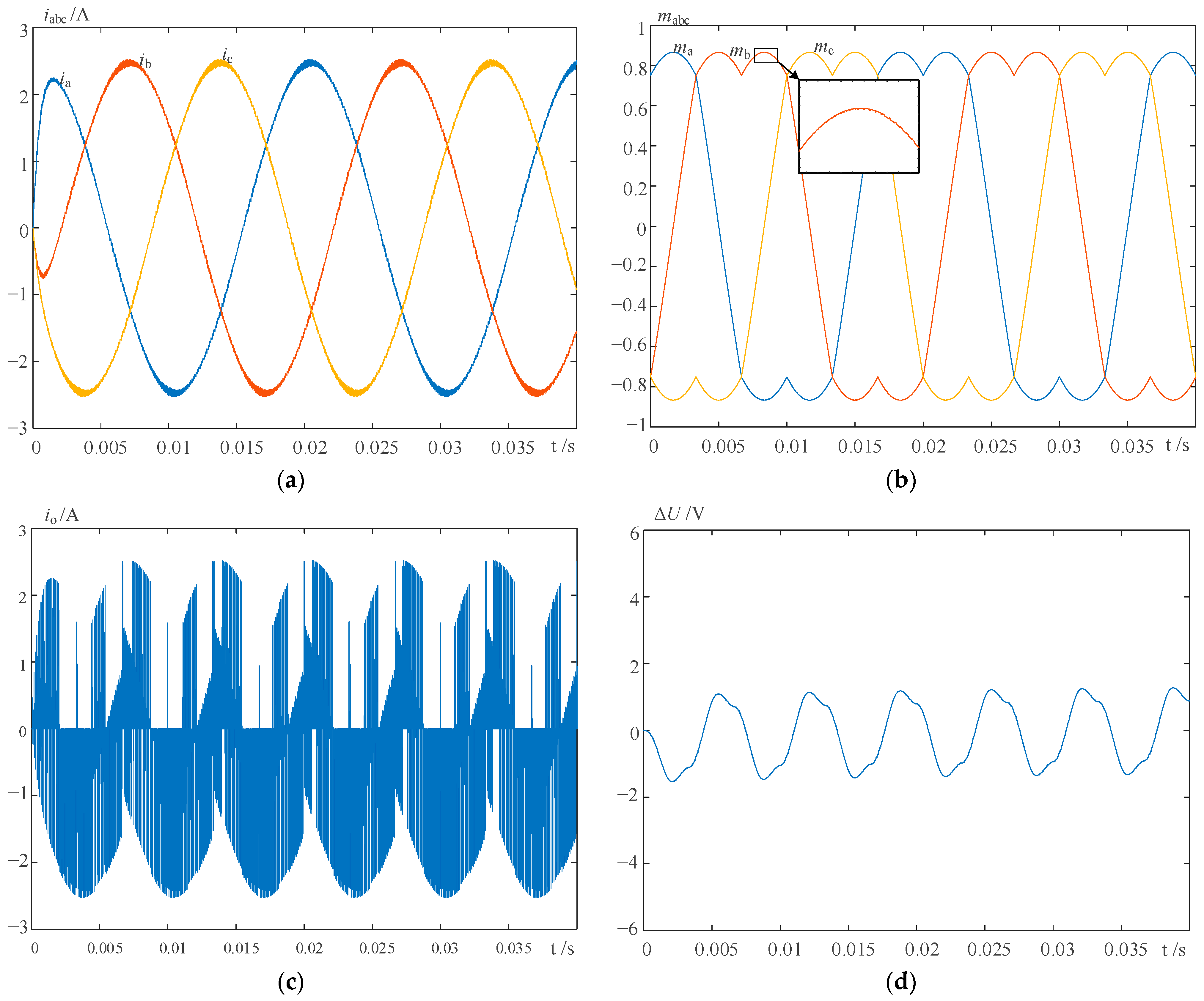
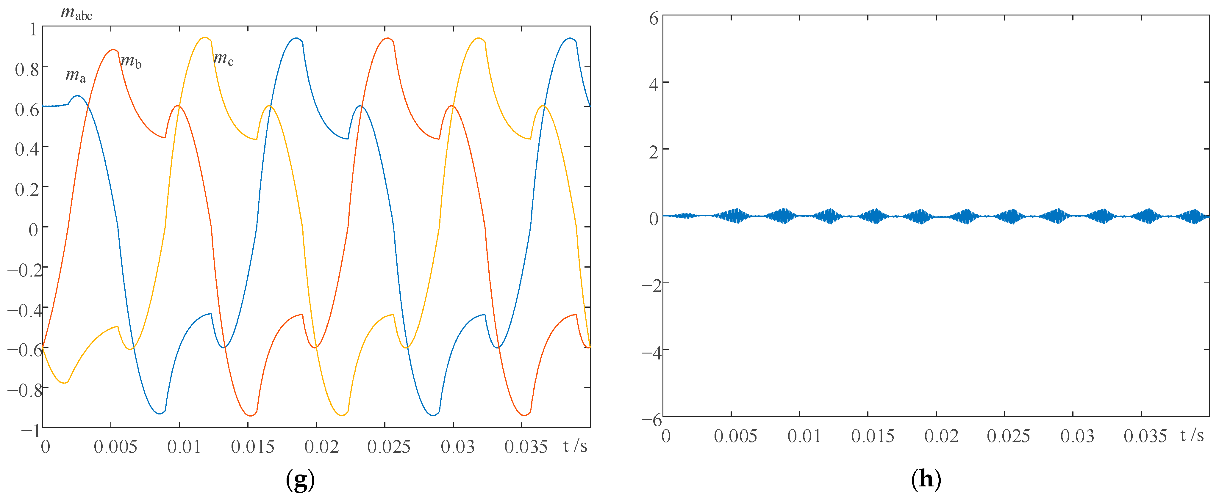
4. Simulation and Experimental Results

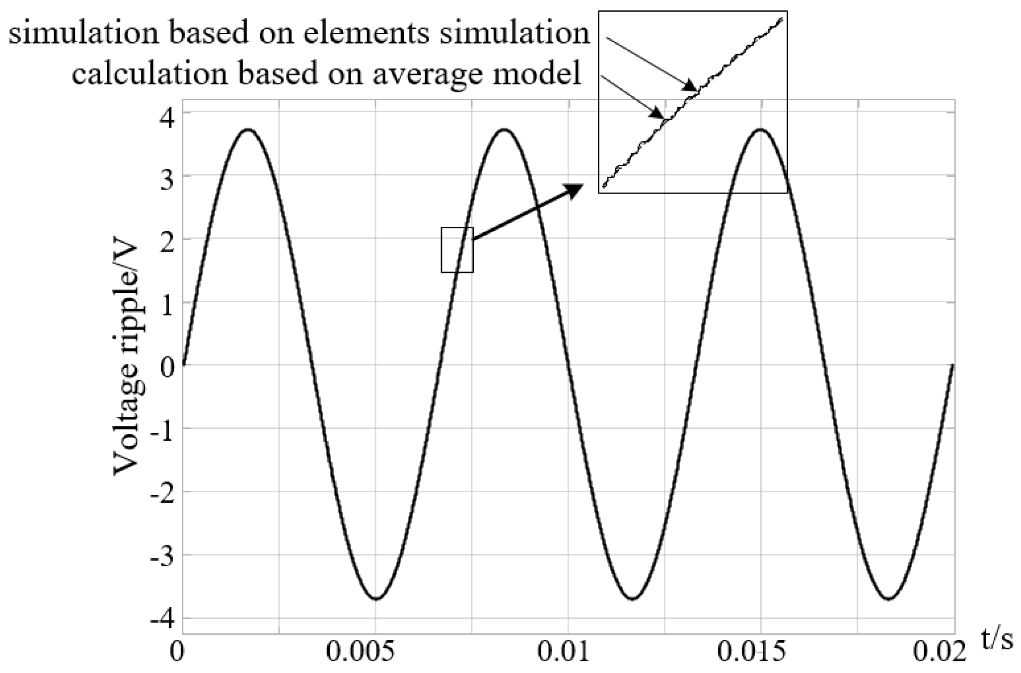
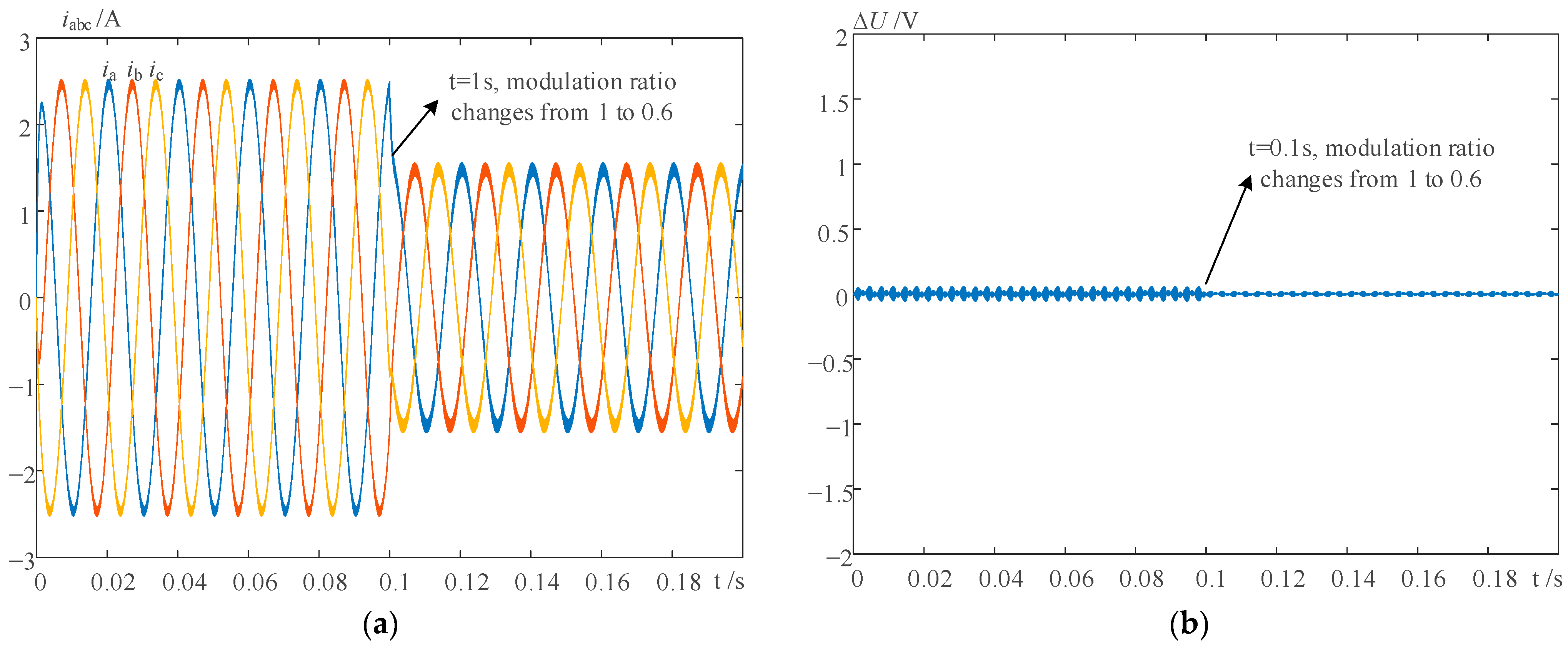
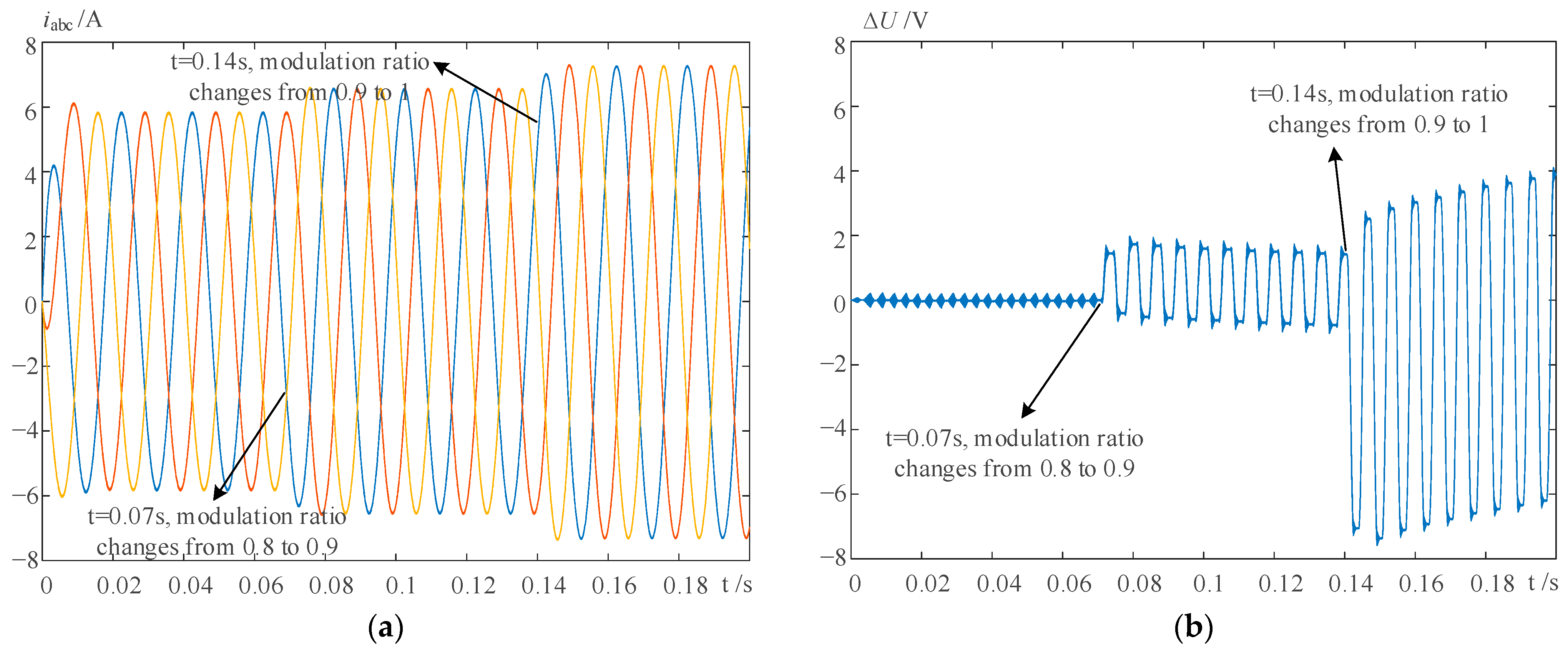
4.1. Simulation Results

To test the feasibility of the proposed method, a three-level NPC inverter system based on MATLAB/Simulink shown in Figure 1 is established. The simulation parameters are presented in Table 3.
Figure 8 shows the simulation results under CBPWM modulation without compensation voltage injection. Among them, i a , i b , and i c are the load current; m a , m b , and m c are the voltage reference signals for modulation; and it can be seen that it is a tradition CBPWM modulation. The neutral-point current fluctuates at three times the frequency. Under this modulation mode, the neutral-point current i o is always positive in some periods and always negative in some periods, and the polarity of positive and negative changes three times in each power frequency cycle. Based on the waveform of i o , it is obvious that there will be three times the frequency of fluctuation on the neutral-point voltage. Additionally, from Figure 8d, the amplitude of three times the frequency of voltage fluctuation is very high.
Figure 9 shows the simulation results under modulation after compensation voltage injection. Among them, i a , i b , and i c are the load current and m a , m b , and m c are the voltage reference signals for modulation, and they are no longer standard sine waves after being injected with a compensation voltage. Figure 9b shows that the modulation wave after compensation does not exceed the limit, so it can achieve self-balance in each switching cycle. For the waveform of i 0 , there are both positive and negative of i 0 during every switching cycle. In addition, the integral of the current i o in each switching cycle is 0. Based on the waveform of i o , it is obvious that the voltage fluctuation on the neutral point is at switching frequency, and the amplitude of this high-frequency voltage fluctuation is almost 0.
Figure 10 shows the simulation results of the proposed method in [22] with the same parameters. The proposed method in [22] uses a PI controller to acquire the adjustable compensation voltage based on the neutral-point voltage. By comparing Figure 9 and Figure 10, the neutral-point voltage fluctuation decreases significantly after the compensation voltage injection of the proposed method [22], but the suppression effect is still far less than that of the method in Figure 9.
Figure 11 shows the influence of the modulation rate m and power angle φ on the fluctuation suppression ability of the proposed method. By contrasting Figure 11b,d, when φ changes from 12 ° to 41 ° , m = 1 can no longer satisfy the requirement of compensation voltage, and there is a lower frequency and much larger amplitude voltage fluctuation in Figure 11b. After the modulation is reduced from 1 to 0.9 in Figure 11e, the amplitude of voltage fluctuation greatly decreased in Figure 11f. In Figure 11g,h, with the further reduction of m = 0.8, the voltage fluctuation is almost 0.
Table 4 shows the THD analysis of the simulation results under different cases. It was observed that the THD is very low and complies with international standards.
Figure 12 and Figure 13 show the dynamic performance of the proposed method. Figure 12 shows the rapid change of the modulation ratio when φ = 12 ° . Based on the pervious analysis, the neutral-point current can achieve self-balance under both modulation ratios. In Figure 11b, there is almost no change of amplitude of neutral-point fluctuation.
Figure 13 shows the rapid change of the modulation ratio when φ = 41 ° . It was observed that, with the change of m from 0.8 to 0.9 and 1, the neutral point starts to show small fluctuations at the time 0.07 s. At 0.14 s, with the m further increased, the amplitude of fluctuation also increased.
To sum up, the proposed method is suitable for low-modulation ratios and high-power factors, and it can achieve voltage variation self-balance in each switching cycle. Even in high-modulation ratios and low-power factor conditions, the proposed method is subject to some limitations. The fluctuation amplitude is still much smaller than that without compensation.

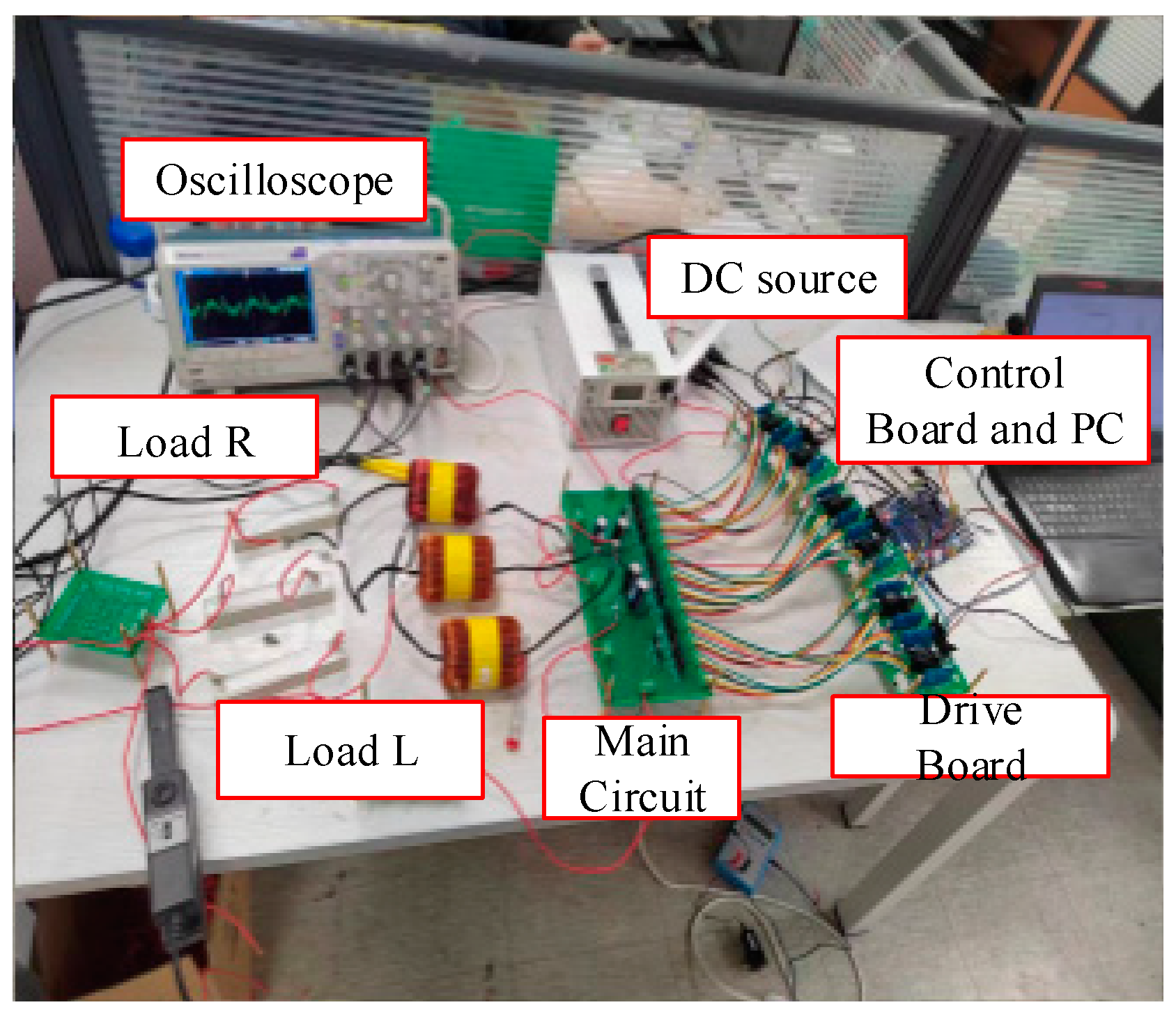
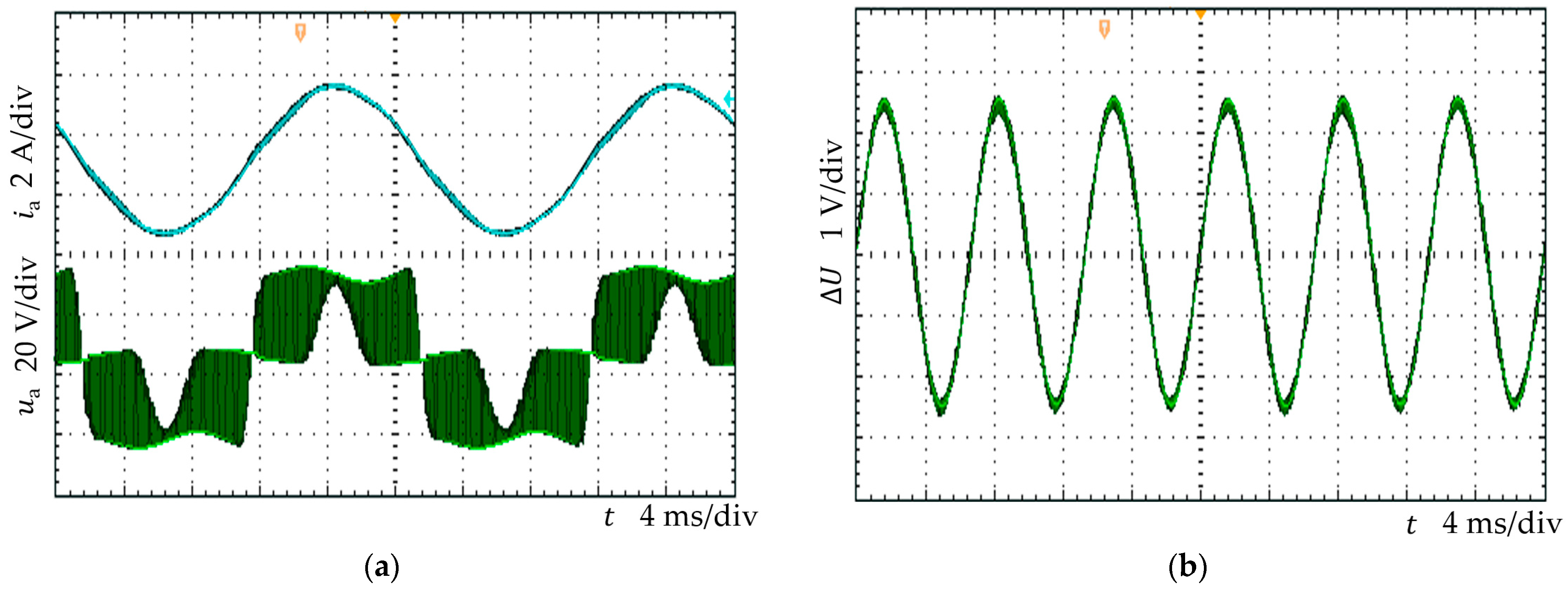
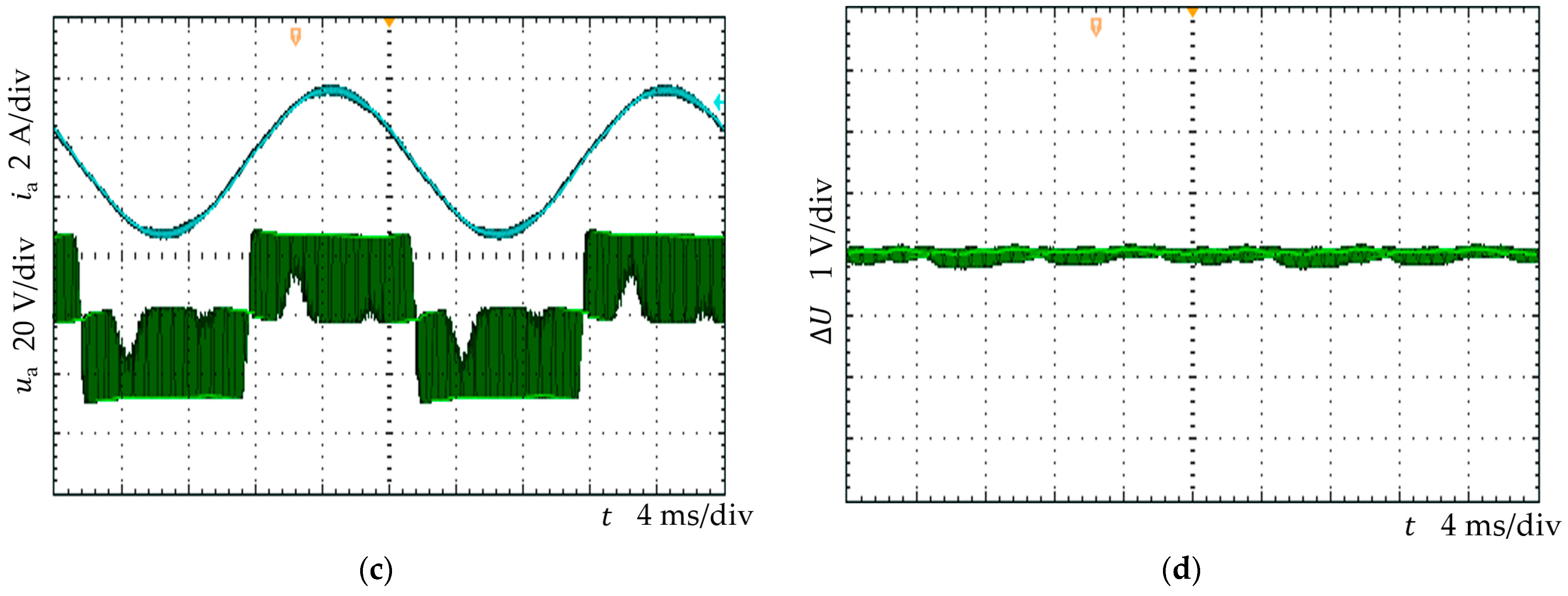
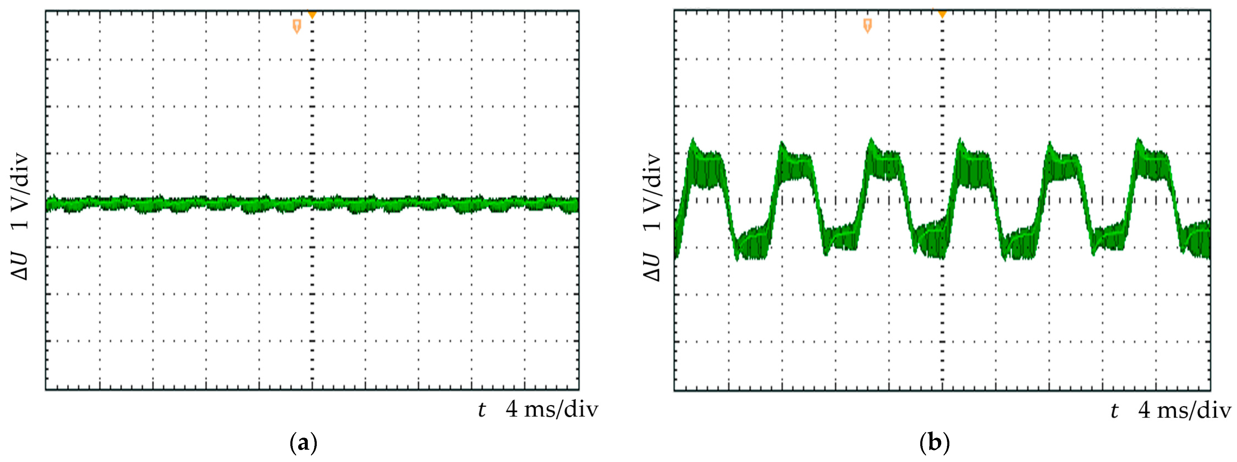
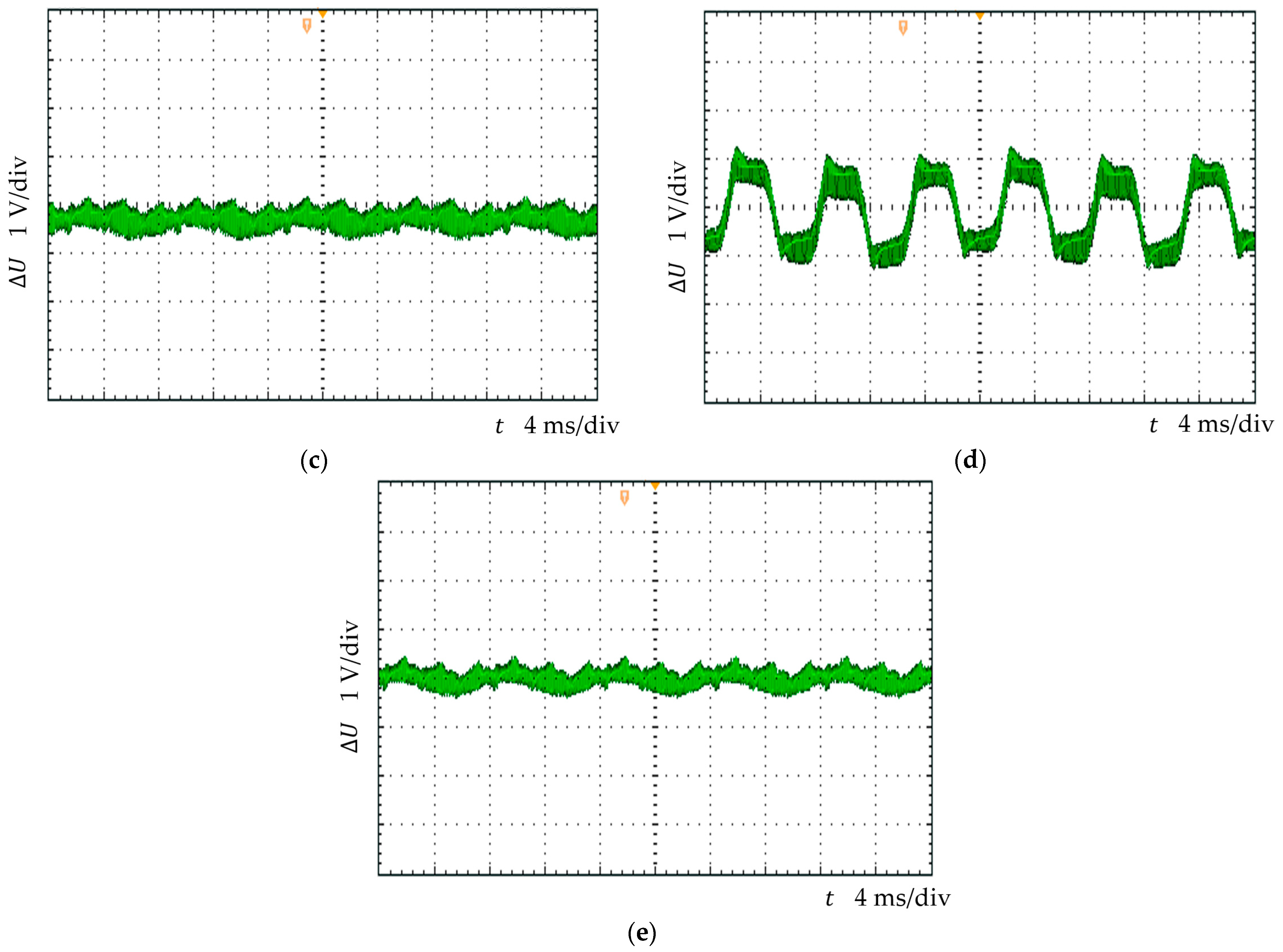
4.2. Experimental Results

To further verify the effectiveness of the proposed method, the low-power prototype in Figure 1 was established as shown in Figure 14. The prototype parameters are presented in Table 5. The prototype components’ specifications are: MOSFET: IRFP260N (50 A/200 V), Diode: RHRP3060 (30 A/600 V), DC-Capacitor: AISHI WH 300 uF, 200 V.
Figure 15 shows the suppression effect of the proposed method on neutral-point voltage fluctuation; (a) and (b) are waveforms before the compensation voltage is injected, while (c) and (d) are waveforms after the compensation voltage is injected according to the proposed method. It is observed that, in Figure 15a, the voltage amplitude of each PWM period fluctuates, and the current also has a large distortion, which is caused by the fluctuation of the neutral-point voltage shown in Figure 15b. However, after the compensating voltage injection using the proposed method, it is observed that the large voltage fluctuation is almost invisible in Figure 15d, and only the high-frequency fluctuation based on the switching period is left. Therefore, the phase voltage amplitude in Figure 15c is more stable among each PWM period and the current waveform has less distortion.
Figure 16 shows the how the modulation rate m and power angle φ influence the fluctuation suppression effectiveness of the proposed method in the prototype experiment. Figure 16a shows that the proposed method can effectively suppress neutral-point voltage fluctuation when m = 1 and φ = 12 ° . As the power angle φ increases to 32 ° , the condition that the compensation voltage does not exceed the limit can no longer be satisfied. The voltage fluctuation as shown in (b) appears at the neutral point under the condition of not completed compensated. At this time, when lowering modulation ratio to 0.9, the condition of compensation voltage is satisfied again, and the neutral-point fluctuation is suppressed again, as shown in Figure 16c. With further increase of φ = 41 ° , the neutral-point fluctuation appears again in (d) and disappears after reducing modulation m = 0.85 shown in (e). By comparing Figure 16a,c, the voltage fluctuation increases because the load resistance is reduced to a quarter and the load current increases to 4 times.

5. Conclusions

This paper proposed a compensation voltage injection method for the suppression of the amplitude of neutral-point voltage fluctuation for a three-level NPC inverter. From the view of neutral-point current, using a mean value model for the neutral-point current during each switching cycle, the voltage fluctuations could be calculated accurately. Then, a high-frequency, switching-cycle-based compensation voltage was calculated and injected into the modulation signal to minimize the voltage variation in each switching cycle. The calculation process of compensation voltage was given, and the influence of the modulation ration and power factor on compensation voltage was analyzed. A MATLAB/Simulink simulation model and a small power prototype were established to verify the proposed method. The conclusions are as follows:
(1)
The proposed average model can accurately calculate the voltage fluctuation of the neutral point. There are only very few discretization errors.
(2)
The proposed method can effectively suppress the voltage fluctuation of the neutral point. In the condition of high-power factor and low-modulation ratio, the voltage variation in each switching cycle can be self-balanced. The amplitude of the voltage fluctuation of the neutral point is much lower than that without compensation.
(3)
The power factor and modulation ratio have a great influence on the suppression ability of the proposed method. Usually, the higher the power factor and the lower the modulation ratio, the better the suppression effect. However, even the proposed method cannot achieve completed compensation in the condition of low-power factor and high-modulation ratio. The amplitude of the neutral-point voltage fluctuation is still much lower than without compensation.

Author Contributions

Writing and editing, G.C. Review, C.G. Funding acquisition, J.B. and L.Z. Supervision and project administration, Z.W. All authors have read and agreed to the published version of the manuscript.

Funding

This research is funded by the National Key R&D Program Funding Projects (2018YFB1503001), the Fund of Shanghai Science and Technology Development (21DZ1207300), and the Shanghai Municipal Commission of Economy and Informatization (GYQJ-2022-1-14).

Data Availability Statement

No new data were created or analyzed in this study. Data sharing is not applicable to this article.

Conflicts of Interest

The authors declare no conflict of interest. The funders had no role in the design of the study; in the collection, analyses, or interpretation of data; in the writing of the manuscript; or in the decision to publish the results.

References

  1. Nabae, A.; Takahashi, I.; Akagi, H. A New Neutral-Point-Clamped PWM Inverter. IEEE Trans. Ind. Appl. 1981, 17, 518–523. [Google Scholar] [CrossRef]
  2. Chen, G.; Gong, C.; Bao, J.; Zhu, L.; Wang, Z. Compensation Voltage Injection Based Neutral Point Voltage Fluctuation Suppression for NPC Converter. In Proceedings of the 2022 Asia Power and Electrical Technology Conference (APET), Shanghai, China, 13 November 2022; pp. 203–208. [Google Scholar]
  3. Liu, P.; Duan, S.; Yao, C.; Chen, C. A Double Modulation Wave CBPWM Strategy Providing Neutral-Point Voltage Oscillation Elimination and CMV Reduction for Three-Level NPC Inverters. IEEE Trans. Ind. Electron. 2018, 65, 16–26. [Google Scholar] [CrossRef]
  4. Oghorada, O.; Li, Z.; Esan, A.; Egbune, D.; Uwagboe, J. Inter-cluster Voltage Balancing Control of Modular Multilevel Cascaded Converter Under Unbalanced Grid Voltage. Prot. Control. Mod. Power Syst. 2022, 6, 289–299. [Google Scholar] [CrossRef]
  5. Wang, Z.; Cui, F.; Zhang, G.; Shi, T.; Xia, C. Novel Carrier-Based PWM Strategy with Zero-sequence Voltage Injected for Three-Level NPC Inverter. IEEE J. Emerg. Sel. Top. Power Electron. 2016, 4, 1442–1451. [Google Scholar] [CrossRef]
  6. Xia, C.; Zhang, G.; Yan, Y.; Xin, G.; Shi, T.; He, X. Discontinuous Space Vector PWM Strategy of Neutral-Point-Clamped Three-Level Inverters for Output Current Ripple Reduction. IEEE Trans. Power Electron. 2017, 32, 5109–5121. [Google Scholar] [CrossRef]
  7. Tsai, M.J.; Chen, H.C.; Tsai, M.R.; Wang, Y.B.; Cheng, P.T. Evaluation of Carrier-based Modulation Techniques with Common-Mode Voltage Reduction for Neutral Point Clamped Converter. IEEE Trans. Power Electron. 2017, 33, 3268–3275. [Google Scholar] [CrossRef]
  8. Jiang, W.; Wang, P.; Ma, M.; Wang, J.; Li, J.; Li, L.; Chen, K. A Novel Virtual Space Vector Modulation With Reduced Common-Mode Voltage and Eliminated Neutral Point Voltage Oscillation for Neutral Point Clamped Three-Level Inverter. IEEE Trans. Ind. Electron. 2020, 67, 884–894. [Google Scholar] [CrossRef]
  9. Jayakumar, V.; Chokkalingam, B.; Munda, J. A Comprehensive Review on Space Vector Modulation Techniques for Neutral Point Clamped Multi-Level Inverters. IEEE Access 2021, 9, 112104–112144. [Google Scholar] [CrossRef]
  10. Li, F.; He, F.; Ye, Z.; Fernando, T.; Wang, X.; Zhang, X. A Simplified PWM Strategy for Three-Level Converters on Three-Phase Four-Wire Active Power Filter. IEEE Trans. Power Electron. 2017, 33, 4396–4406. [Google Scholar] [CrossRef]
  11. Giri, S.K.; Chakrabarti, S.; Banerjee, S.; Chakraborty, C. A Carrier-Based PWM Scheme for Neutral Point Voltage Balancing in Three-Level Inverter Extending to Full Power Factor Range. IEEE Trans. Ind. Electron. 2017, 64, 1873–1883. [Google Scholar] [CrossRef]
  12. Ding, W.; Qiu, H.; Duan, B.; Xing, X.; Cui, N.; Zhang, C. A Novel Segmented Component Injection Scheme to Minimize the Oscillation of DC-Link Voltage Under Balanced and Unbalanced Conditions for Vienna Rectifier. IEEE Trans. Power Electron. 2019, 34, 9536–9551. [Google Scholar] [CrossRef]
  13. Jiang, W.D.; Du, S.W.; Shi, X.F.; Bao, X.H. Hybrid PWM Strategy of SVPWM and VSVPWM for Neutral Point-clamped Three-level Voltage Source Inverter. Proc. CSEE 2009, 29, 47–53. [Google Scholar]
  14. Xia, C.; Shao, H.; Zhang, Y.; He, X. Adjustable Proportional Hybrid SVPWM Strategy for Neutral-Point-Clamped Three-Level Inverters. IEEE Trans. Ind. Electron. 2013, 60, 4234–4242. [Google Scholar] [CrossRef]
  15. Bendre, A.; Venkataramanan, G.; Rosene, D.; Srinivasan, V. Modeling and design of a neutral-point voltage regulator for a three-level diode-clamped inverter using multiple-carrier modulation. IEEE Trans. Ind. Electron. 2006, 53, 718–726. [Google Scholar] [CrossRef]
  16. Chaturvedi, P.; Jain, S.; Agarwal, P. Carrier-Based Neutral Point Potential Regulator With Reduced Switching Losses for Three-Level Diode-Clamped Inverter. IEEE Trans. Ind. Electron. 2014, 61, 613–624. [Google Scholar] [CrossRef]
  17. Pou, J.; Zaragoza, J.; Ceballos, S.; Saeedifard, M.; Boroyevich, D. A Carrier-Based PWM Strategy With Zero-Sequence Voltage Injection for a Three-Level Neutral-Point-Clamped Converter. IEEE Trans. Power Electron. 2012, 27, 642–651. [Google Scholar] [CrossRef]
  18. Xiong, W.; Zhu, X.; Lin, J.; Xie, S.; Sun, Y.; Liu, Y.; Su, M. An Algebraic Modulation Strategy for 3L-NPC Converters With Inherent Neutral-Point Voltage Balance Capability. IEEE Trans. Power Electron. 2022, 37, 7533–7539. [Google Scholar] [CrossRef]
  19. Yu, T.; Wan, W.; Duan, S. A Modulation Method to Eliminate Leakage Current and Balance Neutral-Point Voltage for Three-Level Inverters in Photovoltaic Systems. IEEE Trans. Ind. Electron. 2023, 70, 1635–1645. [Google Scholar] [CrossRef]
  20. Kang, K.P.; Cho, Y.; Ryu, M.H.; Baek, J.W. A Harmonic Voltage Injection Based DC-Link Imbalance Compensation Technique for Single-Phase Three-Level Neutral-Point-Clamped (NPC) Inverters. Energies 2018, 11, 1886. [Google Scholar] [CrossRef]
  21. Hammami, M.; Rizzoli, G.; Mandrioli, R.; Grandi, G. Capacitors Voltage Switching Ripple in Three-Phase Three-Level Neutral Point Clamped Inverters with Self-Balancing Carrier-Based Modulation. Energies 2018, 11, 3244. [Google Scholar] [CrossRef]
  22. Odeh, C.; Kondratenko, D.; Lewicki, A.; Jąderko, A. Modified SPWM Technique with Zero-Sequence Voltage Injection for a Five-Phase, Three-Level NPC Inverter. Energies 2021, 14, 1198. [Google Scholar] [CrossRef]
Figure 1. Topology of three-level NPC inverter.
Energies 16 04409 g001
Figure 2. Space vector diagram of three-level inverter.
Energies 16 04409 g002
Figure 3. Simplified topology under different voltage vectors. (a) Large vectors (11-1); (b) medium vectors (10-1); (c) small vectors (100); (d) zero vectors (000).
Energies 16 04409 g003
Figure 4. Modulation wave generation process and corresponding neutral-point current.
Energies 16 04409 g004
Figure 5. Contrast of average model and element simulation.
Energies 16 04409 g005
Figure 6. Control block diagram of proposed compensation voltage injection method.
Energies 16 04409 g006
Figure 7. Compensation voltage under different modulation ratios m and power angles φ . (a) m = 1, φ = 0. (b) m = 0.8, φ = 0. (c) m = 1, φ = π / 6 . (d) m = 0.8, φ = π / 6 . (e) m = 0.8, φ = π / 3 .
Energies 16 04409 g007aEnergies 16 04409 g007b
Figure 8. Simulation results without proposed voltage compensation when m = 1 and φ = 12 ° . (a) Load current: i a , i b , and i c . (b) Modulation waveform: m a , m b , and m c . (c) Neutral-point current i o . (d) Neutral-point voltage fluctuation Δ U .
Energies 16 04409 g008
Figure 9. Simulation results with proposed voltage compensation when m = 1 and φ = 12 ° . (a) Load current: i a , i b , and i c . (b) Modulation waveform: m a , m b , and m c . (c) Neutral-point current i o . (d) Neutral-point voltage fluctuation Δ U .
Energies 16 04409 g009
Figure 10. Simulation results with proposed voltage compensation when m = 1 and φ = 12 ° . (a) load current: i a , i b , and i c . (b) Modulation waveform: m a , m b , and m c . (c) Neutral-point current i o . (d) Neutral-point voltage fluctuation Δ U .
Energies 16 04409 g010
Figure 11. Simulation results with proposed voltage compensation under different m and φ . (a) Modulation wave m a b c when m = 1 and φ = 12 ° . (b) Neutral-point voltage fluctuation Δ U when m = 1 and φ = 12 ° . (c) Modulation wave m a b c when m = 1 and φ = 41 ° . (d) Neutral-point voltage fluctuation Δ U when m = 1 and φ = 41 ° . (e) Modulation wave m a b c when m = 0.9 and φ = 41 ° . (f) Neutral-point voltage fluctuation Δ U when m = 0.9 and φ = 41 ° . (g) Modulation wave m a b c when m = 0.8 and φ = 41 ° . (h) Neutral-point voltage fluctuation Δ U when m = 0.8 and φ = 41 ° .
Energies 16 04409 g011aEnergies 16 04409 g011b
Figure 12. Dynamic response of the inverter for step changes in the modulation ratio when φ = 12 ° . (a) Load current response. (b) Neutral-point voltage fluctuation response.
Energies 16 04409 g012
Figure 13. Dynamic response of the inverter for step changes in the modulation ratio when φ = 41 ° . (a) Load current response. (b) Neutral-point voltage fluctuation response.
Energies 16 04409 g013
Figure 14. A photo of the established prototype.
Energies 16 04409 g014
Figure 15. Experiment results for the proposed method when m = 1 and cos φ = 0.98 . (a) Waveform of phase voltage u a and phase current i a under modulation without proposed method. (b) Waveform of neutral-point voltage fluctuation Δ U under modulation without proposed method. (c) Waveform of phase voltage u a and phase current i a under modulation with proposed method. (d) Waveform of neutral-point voltage fluctuation Δ U under modulation with proposed method.
Energies 16 04409 g015aEnergies 16 04409 g015b
Figure 16. Neutral-point voltage fluctuation Δ U with proposed voltage compensation under different m and φ . (a) m = 1, φ = 12 ° and R = 10 Ω . (b) m = 1, φ = 32 ° and R = 2.5 Ω . (c) m = 0.9, φ = 32 ° and R = 2.5 Ω . (d) m = 0.9, φ = 41 ° and R = 2.5 Ω . (e) m = 0.85, φ = 41 ° and R = 2.5 Ω .
Energies 16 04409 g016aEnergies 16 04409 g016b
Table 1. Output levels and switching states.
u a o Q 1 Q 2 Q 3 Q 4 S a
+ U d c /2ONONOFFOFF1
0OFFONONOFF0
U d c /2OFFOFFONON−1
Table 2. Relationship between voltage vectors and neutral-point current.
Vector i o Vector i o Vector i o
ONN i a POO i a ONP i a
POP i b ONO i b PON i b
NNO i c OOP i c PNO i c
OPP i a NOO i a OPN i a
NON i b OPO i b NOP i b
PPO i c OON i c NPO i c
Table 3. Simulation parameters.
ParametersValue
DC voltage U d c /V50
Switching frequency/kHz10
DC capacitor C 1 /μF300
DC capacitor C 2 /μF300
( φ = 12 ° ) Inductor L/mH5
( φ = 12 ° ) Resistor R10
( φ = 41 ° ) Inductor L/mH7
( φ = 41 ° ) Resistor R2.5
Table 4. THD analysis of the simulation results.
THD of iabc under Different CasesTHD, Amp of 2nd, Amp of 5th
Case1: m = 1, φ = 12 ° (SPWM without compensation)
Case2: m = 1, φ = 12 °
1.90%, 0.32%, 1.60%
1.32%, 0%, 0.007%
Case3: m = 1, φ = 41 ° 0.69%, 0.12%, 0.49%
Case4: m = 0.9, φ = 41 ° 0.45%, 0.16%, 0.12%
Case5: m = 0.8, φ = 41 ° 0.45%, 0.01%, 0%
Table 5. Experimental parameters.
ParametersValue
DC voltage U d c /V50
Switching frequency/kHz10
DC capacitor C 1 /μF300
DC capacitor C 2 /μF300
( φ = 12 ° ) Inductor L/mH5
( φ = 12 ° ) Resistor R10
( φ = 41 ° ) Inductor L/mH7
( φ = 41 ° ) Resistor R2.5
Disclaimer/Publisher’s Note: The statements, opinions and data contained in all publications are solely those of the individual author(s) and contributor(s) and not of MDPI and/or the editor(s). MDPI and/or the editor(s) disclaim responsibility for any injury to people or property resulting from any ideas, methods, instructions or products referred to in the content.

