1. Introduction
A DC-DC boost converter is a solution of great importance in applications with a noninsulated power supply and power factor correction (PFC) systems [
1]. The converter can be used in a wide range of applications and can be designed to use different types of switches, including IGBTs. IGBTs remain a very advantageous solution considering the cost-per-watt calculation in the appropriate frequency range. Therefore, IGBT switches with a rated voltage of 650 V can be found in single-phase applications with front PFCs, such as on-line uninterruptible power supplies (UPSs) or AC-AC drive systems.
An important portion of boost converter power losses are associated with its turn-off process. However, they can be reduced by implementing soft switching. The publication [
2] presents an analysis of the soft switching process of an IGBT transistor and shows that it allows the reduction of power losses in the boost converter.
The reduction of switching losses can be achieved by using low-complex additional circuits implemented in a classic converter. The switching turn-off loss decrease based on the idea of an auxiliary switching cell (ASC), which reduces the voltage rise across the transistor (
duDS/
dt), was demonstrated in three-level neutral-point-clamped (NPC) inverters (VSI) in [
3]. In [
4], the method for turn-off loss reduction was demonstrated in a boost converter with auxiliary circuits. The principle of turn-off loss reduction, proposed in [
4], assumes that the rate of increase in the
UCE collector–emitter voltage during the shutdown of the transistor is slow enough to complete the current commutation with a low part of the power loss. The increase in
UCE voltage is reduced by an additional capacitor charged to the output voltage before the shutdown process. The optimal voltage value across the auxiliary capacitor is at the level of the output voltage. These conditions are obtained when the converter shown in [
4] operates with a voltage gain of less than double. At higher gain, the boost converter presented in [
4] requires other auxiliary circuits to achieve effective reduction of turn-off losses. The implementation of the ASC concept for a DC-DC converter has been demonstrated in [
4] and previously in patents [
5,
6,
7]. An advantageous feature of the system proposed in [
4] is its relatively simple ASC system, consisting of two diodes and an auxiliary capacitor and inductor. However, for voltage amplification greater than two, such passive ASC does not provide optimal conditions to reduce switching losses.
In a boost topology, the soft switching technique can be achieved by implementing different kinds of auxiliary commutation circuits and control [
8,
9,
10,
11,
12,
13,
14,
15,
16,
17,
18,
19,
20,
21,
22,
23,
24,
25,
26,
27,
28,
29,
30,
31,
32,
33,
34]. The concepts presented in the literature [
8,
9,
10,
11,
12,
13,
14] are based on the use of passive auxiliary circuits. The implementation of soft switching in a suitable controlled interleaved circuit with output capacitances of transistors is shown in [
8,
9,
10,
11]. In [
8], soft switching operation in boundary conduction mode (BCM) was demonstrated, and in [
9], ZVS near the critical conduction mode (CRM). In the DC-DC converter presented in [
10], the current of inductors is continuous to achieve ZVS in an auxiliary inductor.
Publications [
12,
13] present auxiliary circuits based on
L,
C elements and diodes using resonant circuits. These circuits are characterized by a low number of elements and low complexity. However, some inductive elements are located in the power circuit in series with the transistor. The snubber system shown in [
14] provides the zero-voltage transition (ZVS) and zero-current switching (ZCS) of the boost converter. The circuit uses a capacitor, coupled chokes, and diodes, and the inductive element and diode are placed in the converter power circuit.
Publications [
15,
16,
17,
18,
19,
20,
21,
22,
23,
24,
25,
26,
27,
28,
29,
30,
31,
32,
33,
34] present concepts for the implementation of zero-voltage commutation (ZVT) in a boost converter with auxiliary circuits, controlled by switches and diodes. In the area of these active systems, solutions based on circuits containing transistors and diodes, as well as the
L and
C passive components, are also used. Magnetically coupled elements [
19,
20,
21,
22,
23] are also implemented in active auxiliary circuits for ZVT which may require a more complex design approach. In [
24,
25,
26,
27,
28,
29], resonant circuits are also implemented in active auxiliary circuits for ZVT where [
24,
25,
26,
27] demonstrate development of a ZVT snubber topology, [
28] an auxiliary resonant circuit configured in H-bridge, and [
29] a concept of topology characterized by low-voltage ringing.
Soft-switching operation in a PWM DC-DC boost converter can be also achieved with the implementation of switched-capacitor-based (SC) circuits [
30,
31]. In [
30], the operation of a boost converter with a capacitor-switched snubber attached is demonstrated. The snubber circuit is achieved without any inductive components which is a benefit of some SC circuits. In [
31], a converter with embedded SC circuits and its soft-switching ability is demonstrated.
Since the boost topology is a typical part of PFC rectifiers, active snubbers allow a reduction in switching losses in PFC systems as well, which is demonstrated in [
32,
33,
34].
The soft-switching concept method proposed in this paper is based on an active ASC system where improved conditions for the soft shutdown of the transistor over a large range of output voltage regulation are achieved. Compared to the converter capabilities presented in [
4], the proposed system allows for the effective reduction of turn-off losses for a larger voltage gain range (also for
G > 2). The investigated converter uses an active auxiliary circuit with low complexity and simple control, which is a beneficial feature of this solution. The presented method can be used in a continuous conduction model (CCM) as well as in a discontinuous conduction mode (DCM) of the boost converter operation at variable duty cycles and it does not require regulation of the switching frequency when the load varies. The proposed system improves the parameters of the converter proposed in [
4]. It uses the analogous concept of reducing the rate of voltage increase across the transistor and the auxiliary discharge circuit of the auxiliary capacitor. However, a new active circuit and control method for auxiliary capacitor charging is proposed, supporting the operation of the system presented in [
4], which improves the ZVT for
G > 2.
This article is organized as follows.
Section 2 demonstrates the concept of the proposed circuit and control method for soft switching in the boost converter.
Section 3 presents analyses related to the selection of converter parameters, and
Section 4 presents experimental results with waveforms and measured efficiency.
2. Principle of Operation
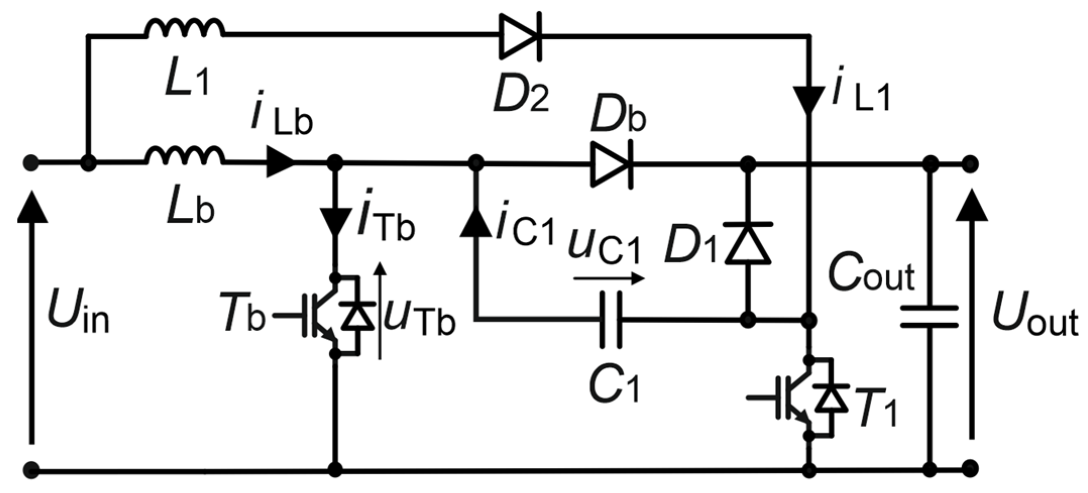
The proposed DC-DC boost converter is presented in
Figure 1. The operation of the power circuit of the converter is the same as in the classic boost DC-DC converter. The voltage gain (
Uout/
Uin) depends on the duty cycle of the main transistor switching.
In the proposed boost converter (
Figure 1), the auxiliary circuits composed of the devices
T1,
D1,
D2,
C1, and
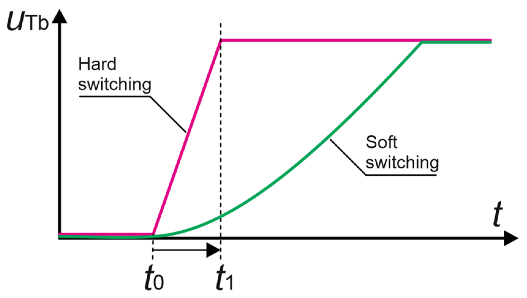
L1 are used for soft-switching implementation. The soft switching is achieved in the proposed circuit when the voltage across the main transistor rises slowly enough to reduce turn-off losses (
Figure 2). The function of the auxiliary circuit components is described in
Table 1.
2.1. Zero-Voltage-Switching ZVS of Turn-Off Condition
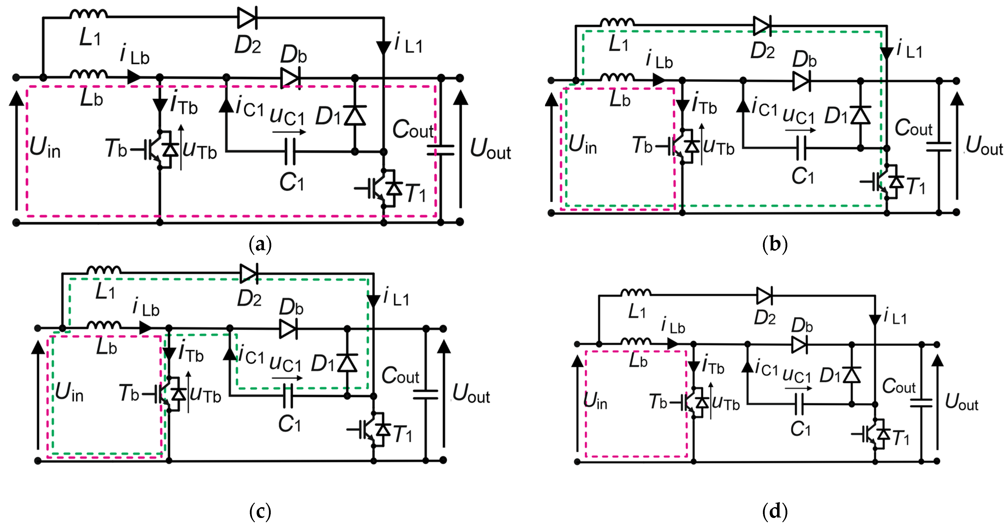
Figure 3 presents stages of operation in the converter when the main transistor is turned off. In the proposed circuit, ZVS occurs during the turning off of the main transistor
Tb. From
Figure 3 it can be seen that voltage across the
Tb is:
where
uout is the output voltage and
uC1 is the voltage across the capacitor
C1.
If the capacitor
C1 is charged to the output voltage, the slow voltage rise across the
Tb transistor starts at zero, which creates optimal conditions for ZVS operation (at the time-point indicated as
t0 in
Figure 2):
where
uTb(
t0) and
uC1(
t0) is the voltage across the transistor
Tb and the capacitor
C1 at the time-point
t0.
ZVS turn-off is not achieved when the
C1 capacitor voltage is below the output voltage level at beginning of
Tb turn-off.
Figure 4 presents model waveforms at the turn off of the
Tb transistor in the boost converter in the case when the auxiliary capacitor is properly charged (
Figure 4a) and when its charging is below the output voltage level (
Figure 4b).
2.2. Optimal ZVS Conditions
The proposed converter contains the circuit which allows for auxiliary capacitor
C1 charging. The charging circuit is composed of the resonant choke
L1, the
C1 capacitor, diodes
D2, and components of the power circuit
Tb as well as the active component
T1. When the
T1 transistor is not used, the
C1 capacitor is charged from the input voltage in an oscillatory circuit to the following value:
where
Uin is the supply voltage, and
uC1max and
uC1init is the maximum and initial voltage of the capacitor
C1.
At rated conditions, the initial voltage of the C1 capacitor is zero and the capacitor can be charged to 2Uin. In such a case, the ZVS conditions may not be assured for two following reasons:
- -
The converter operates with voltage gain G > 2. In such a case, the maximal voltage across the C1 capacitor is below the output voltage: uC1max = 2Uin(t0) < GUin. Assuming low voltage ripple across the input capacitor, this relationship can be simplified to the following form: uC1max = 2Uin < GUin.
- -
Nonzero initial voltage in the C1 capacitor charging process. This can occur when the converter operates in a light load and therefore has insignificant importance from an efficiency optimization viewpoint.
Therefore, the ZVS conditions are not accomplished in the case where the converter operates with voltage gain G > 2 when C1 capacitor is charging with the use of an auxiliary diode-inductor circuit (D2, L1). To create fair ZVS conditions for Tb, an active C1 capacitor charging circuit can be used. The active charging circuit utilizes an additional T1 transistor along with D2, L1 components.
2.3. The Active Auxiliary Circuit for ZVS Operation
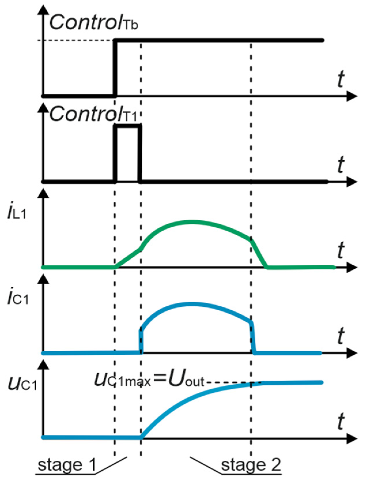
Operation of the active auxiliary charging circuit assumes the use of the T1 transistor to improve C1 capacitor charging through an increase in the initial current of the L1 inductor. This leads to an increase in the charging voltage of capacitor C1 to meet the conditions of ZVS in the system (2).
Figure 5 shows the idealized waveforms related to the operation of an auxiliary circuit with the transistor
T1 to obtain a nonzero value of the initial current when charging the capacitor
C1. During this process of charging the
C1 capacitor, the following stages are used:
- -
Stage 1 (
Figure 6b): the main switch
Tb is turned on along with the
T1 transistor. The
C1 capacitor is not charged in this state, but the current of the
L1 inductor rises.
- -
Stage 2 (
Figure 6c): after a sufficient time, the transistor
T1 is switched off and the process of charging
C1 from the nonzero initial current conditions in the
L1 choke begins. The switching time of transistor
T1 is much shorter than the half-period of the pulse of the main transistor
Tb.
The charging of
C1 is continued in the resonant circuit and after the charge current (
iL1) disappears, the converter remains in the typical main circuit state, in which the main transistor
Tb is switched on (
Figure 6d). The process of the
C1 capacitor is controlled in the same way in CCM and DCM modes of operation.
3. Parameters of Auxiliary Circuit Devices and Control
The capacitance of the auxiliary capacitor
C1 determines collector–emitter voltage rise across the
Tb transistor (d
uTb/d
t—
Figure 4). Directly after the
Tb is turned off, the inductor
Lb current (
iL1) flows through the
C1 capacitor. During this time interval the
C1 is being discharged and the voltage across the
Tb transistors rises according to (1) (
Figure 4). Assuming a constant value of the inductor’s current during the commutation time interval, the
uC1 voltage derivative is the following:
where
ILb is the average
Lb inductor’s current during the time when the
C1 capacitor is discharging (for
uTb <
Uin the inductor’s current is still rising, therefore the current
ILb is slightly below the maximum
ILbm; however, for the model of capacitor selection it can be assumed that
ILb =
ILm).
At rated conditions, the
C1 capacitor is charged to the output voltage. Therefore, the
C1 capacitance is selected according to the following formula:
where
tC is the time period when the
C1 capacitor is discharging (
Figure 3c).
The ILm and Uout are determined by design requirements, but the time interval when uC1 rises is set based on the rate of switching-losses reduction.
The most critical issue for the ZVS operation of the converter is the
C1 capacitor charging process. The
C1 capacitor is charged from the input voltage source. When the voltage gain of the converter is
GU > 2, the
C1 capacitor must be charged with the use of the auxiliary active circuit which allows it to achieve the optimal ZVS conditions:
The charging of the
C1 capacitor starts by switching the transistor
T1 simultaneously with the transistor
Tb. As a result, the
L1 choke current increases to (
Figure 5 and
Figure 6) the value:
where
tl is the time when the transistor
T1 is switched on.
In the next stage, after switching off the transistor
T1, the capacitor
C1 is charged in a circuit composed of elements
L1,
D2,
C1, and
Tb, with initial current conditions
I0 =
IL1max, and voltage
UC10 which should be rated 0. The waveform of the voltage across the capacitor and its current, for the given initial conditions, is described by the following relationships:
The charging ends after one oscillation time, i.e., for
. It denotes that the capacitor
C1 is charged to the value:
The initial condition of the
C1 capacitor charging current, assuming that the capacitor should be charged to the value of the output voltage, is the following:
The duration of the switching pulse of the transistor
T1, in which the choke
L1 current increases linearly, should be as follows:
For the converter’s voltage gain
the relationship (14) can be expressed in the following form:
From Equation (15), it follows that the duration of the T1 transistor on-state pulse-switching varies along with the voltage gain of the converter. However, it can be tuned using the relation (15) and feedback from the duty cycle or the voltage gain measurement.
The use of the ASC system does not change the voltage stress across the transistor and the diode in the power circuit of the converter
UTbm =
UDbm =
Uout. Based on the analysis of the operating stages of the system shown in
Figure 3 and
Figure 6, it also follows that the voltage stress across the active elements
T1 and
D1 of the ASC circuit is also equal to the value of the output voltage. Voltage stress across the
D2 diode reaches the value equal to a difference in output and input voltage. The stages of operation from which this follows are shown in
Table 2.
4. Experimental Results
The new concept of the boost system with soft turn-off and the efficiency of the converter have been experimentally verified.
Table 3 lists semiconductor and passive components used in experimental systems, while
Figure 7 shows a photograph of the laboratory setup.
The supply voltage of the converter was set at the level of Uin = 100 V, with the output at the level of Uout = 400 V, so that it was possible to inspect the operation of the proposed system at high gain. The tests were carried out for different switching frequencies of the transistor and load power up to 3.5 kW. The maximum junction temperature of the semiconductor elements used are typical (150 °C and 175 °C).
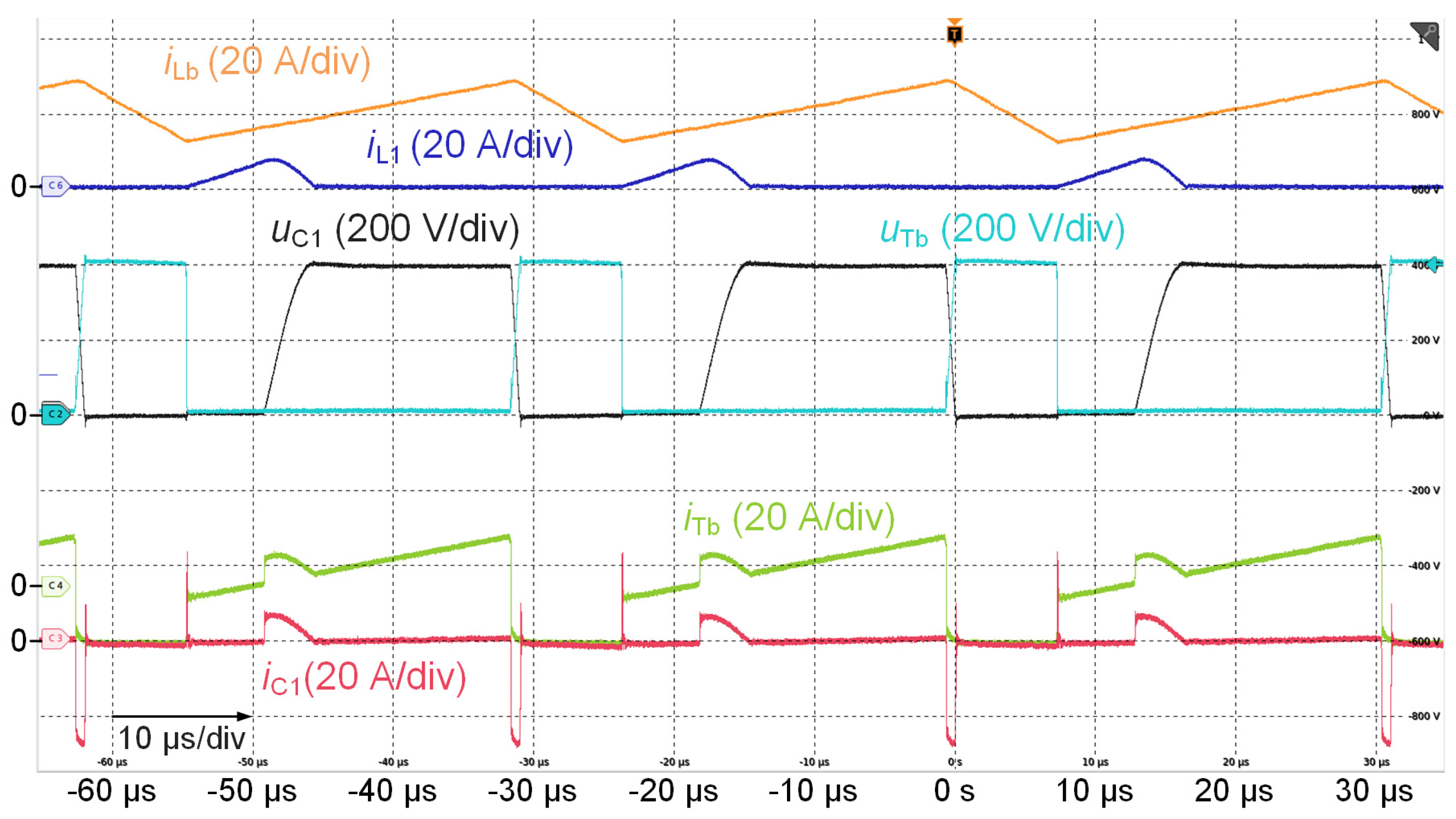
Figure 8 shows a set of waveforms demonstrating the operation of the system according to the soft switching concept. These results show that the main current waveform of the converter choke is analogous to that of a classic boost converter. The current of the auxiliary choke increases linearly in the first stage after switching on the transistor
Tb, and then participates in the oscillation charging the capacitor
C1. In the current waveform of capacitor
C1, its charging with nonzero initial current conditions and discharge with the main choke current
Lb are seen. Similarly, the correct operation of the soft-switching circuits can be determined from the DCM waveforms shown in
Figure 9. The waveforms shown in
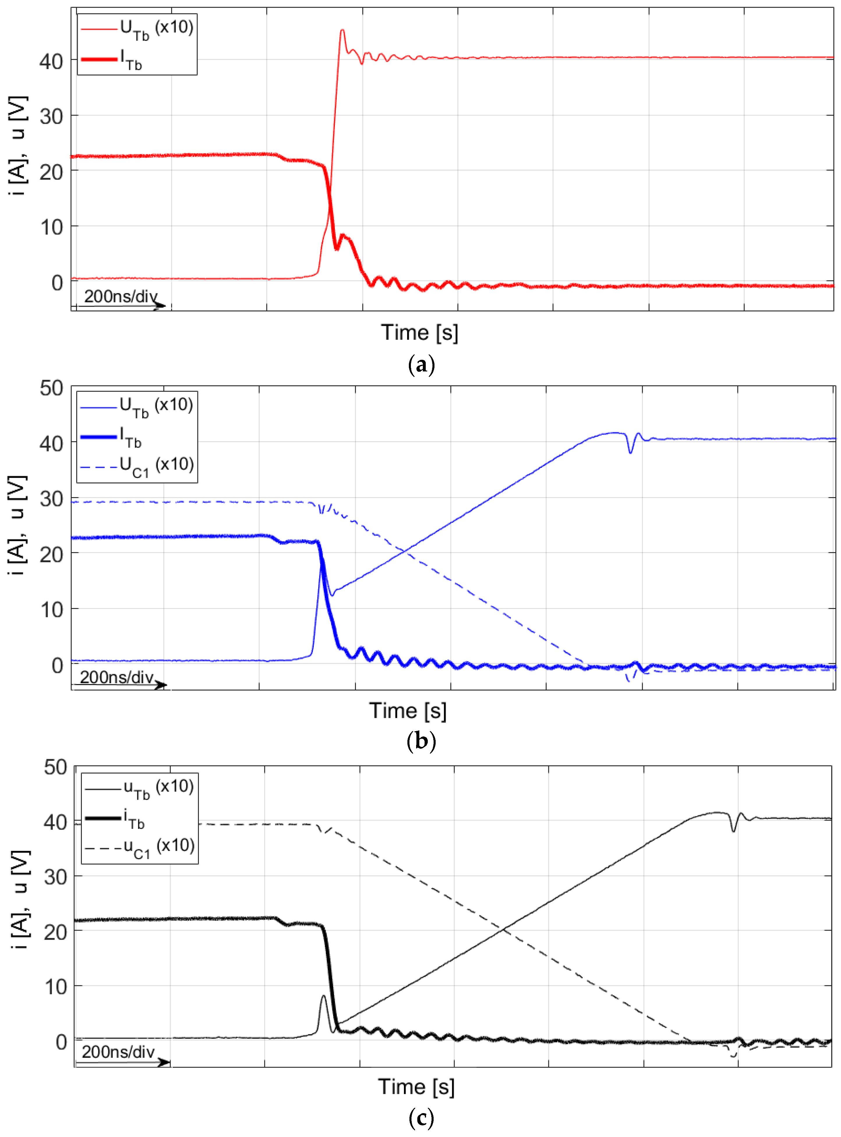
Figure 10 demonstrate the effectiveness of the applied loss-reduction concept when the transistor is turned off in the boost converter for
GU > 2 gain. The proposed system slows down the collector–emitter voltage across the
Tb transistor and the improvement over [
4] is very clear. Of course, this is also a solution that significantly reduces switching losses compared to the classic boost system. In the tests, the results of which are shown in
Figure 8 and
Figure 9, the transistors
Tb and
T1 are switched on simultaneously (in the time-instant where the drain-source voltage of Tb falls down), and when the
T1 transistor is turned off the
C1 current starts to flow and the
C1 capacitor is charged.
The efficiency measurements confirm the reduction of energy losses by applying the soft turn-off concept, as shown in
Figure 11,
Figure 12 and
Figure 13. The proposed converter efficiency is compared to the classic boost converter and the converter presented in [
4]. In all cases, results of efficiency were achieved in the same basic setup for the voltage gain
GU = 4; thus, this article also expands the knowledge of the system studied in the literature [
4].
Figure 11 and
Figure 12 present results of efficiency versus power at 32.2 kHz and 48.7 kHz according to typical characteristics, while the results shown in
Figure 13 show the efficiency relationship versus switching frequency. From the results presented in
Figure 11,
Figure 12 and
Figure 13 it can be seen that the proposed system is more efficient than both the boost converter and the concept from [
4].
The difference becomes greater as the switching frequency increases, which creates greater possibilities for designing boost converters with a higher switching frequency and smaller volume of passive components. The ASC system introduces additional switching losses, as can be seen in the results shown in the
Figure 12 where, for low power, the proposed system is less efficient than the converter shown in [
4]. However, the switching losses of the ASC circuit are so insignificant that at 2kW increasing the switching frequency is beneficial for the proposed system (
Figure 13).
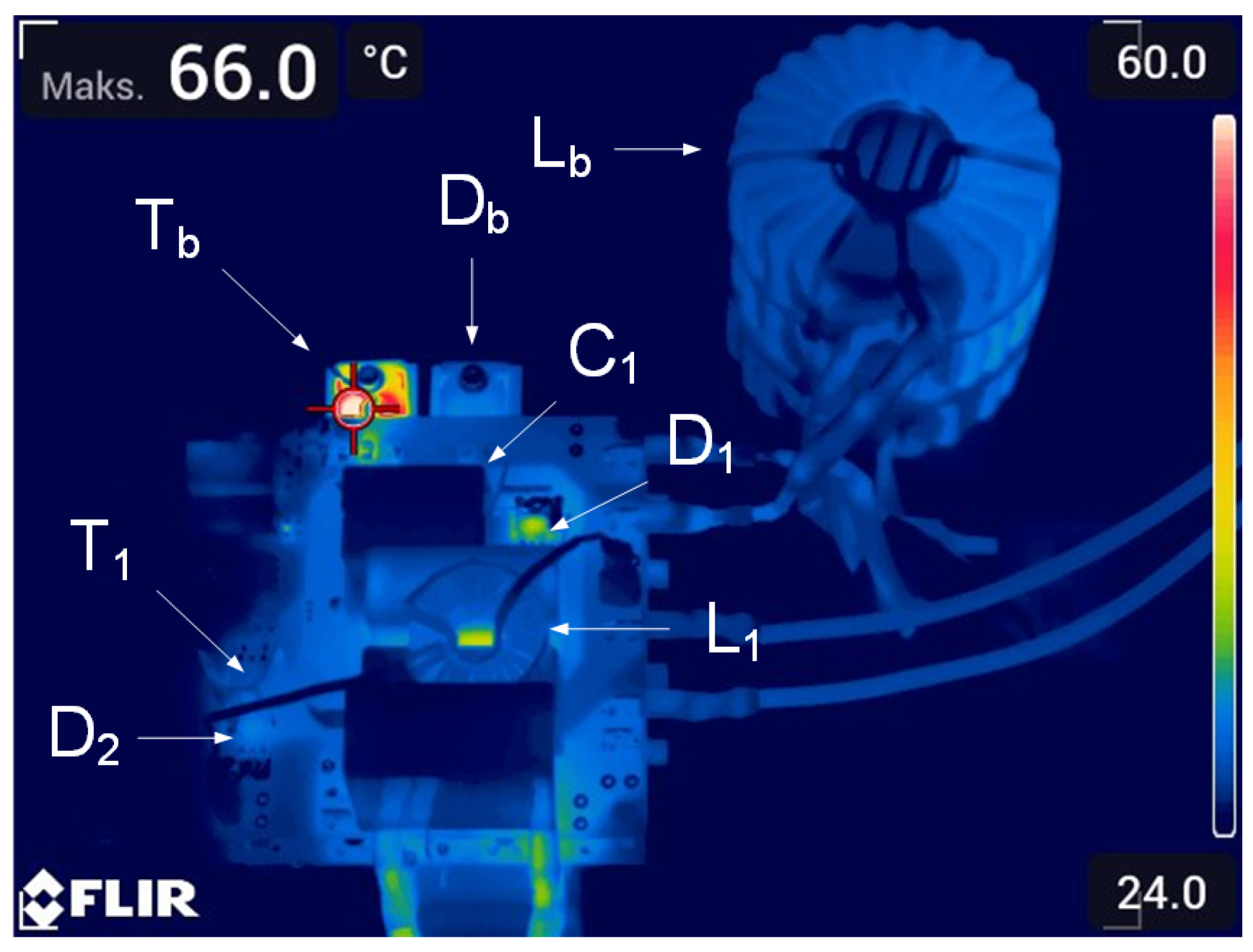
Figure 14 presents a thermal photo of the proposed laboratory converter. The recording was performed with a Flir E96 thermal imaging camera. The parameters of the camera were: resolution 640 × 480, emissivity 0.98, and range of temperature from −20 °C to +120 °C. The reflected and the ambient temperature was 20 °C. The converter and chokes were placed on a nonreflective rubber bench mat. The measurement was performed from approximately 1 m distance using neutral white LED light illumination. The measurements were made in steady state for supply voltage
Uin = 100 V, output power
Pout = 2 kW, and pulse frequency
fsw = 32.2 kHz. The output voltage was 400 V. The highest temperature occured on the transistor
Tb and was about 60 °C. Another element with a noticeable temperature of about 35 °C was the diode
D1. The temperature of the remaining elements did not exceed 30 °C.
Figure 14 exhibits that the power losses of the boost elements outside the
Tb transistor are insignificant, and the power losses of the additional system are negligible.
5. Conclusions
This article presents a new concept of turn-off power losses reduction in the boost converter for operation with voltage gain higher than two. The proposed auxiliary commutation circuit allows for ZVS during transistor turn-off. An active part of the auxiliary circuit assures its proper operation at high voltage gain.
It was shown that the proposed system has a higher efficiency than the classic IGBT-based boost converter. It was also shown that the new solution allows for higher efficiency than a reference circuit that implements soft switching in a way that is effective for gains lower than two.
The proposed system is relatively simple and uses a low number of components. Its control is synchronized with the switching of the main transistor. At low voltage gains the auxiliary circuit operates effectively as a passive circuit.
This article presents experimental results in the form of current and voltage waveforms as well as the results of heating the circuit obtained via thermal imaging measurement. From the heating results, it is clear that the most lossy element in the tested system is the IGBT transistor; therefore, reducing its losses is justified to obtain a more even distribution of losses in the real system.
The proposed system can be very advantageous in boost converter systems with IGBT transistors with high Eoff energy lost during turn-off and allows for an increase in the switching frequency of the boost converter and a reduction in the volume of passive components.
