Article

Evaluation of Voltage-Matched 2T Multi-Junction Modules Based on Monte Carlo Ray Tracing

1
Istituto per la Microelettronica e Microsistemi, Consiglio Nazionale delle Ricerche (CNR-IMM), VIII Strada, 5, Z.I., 95121 Catania, Italy
2
Dipartimento di Fisica e Astronomia, Università degli Studi di Catania, Via S. Sofia, 64, 95123 Catania, Italy
3
Enel Green Power, Contrada Blocco Torrazze sn—Z.I., 95121 Catania, Italy
*
Author to whom correspondence should be addressed.
Energies 2023, 16(11), 4292; https://doi.org/10.3390/en16114292
Submission received: 21 April 2023 / Revised: 16 May 2023 / Accepted: 22 May 2023 / Published: 24 May 2023
(This article belongs to the Topic Photovoltaic Materials and Devices)

Abstract

:
As Si single-junction technology is approaching its Shockley–Queisser theoretical limit, relevant efforts are being expended towards the development of multi-junction modules. In this work, we employ an optical model based on Monte Carlo ray tracing to compare four different multi-junction modules in a voltage-matched two-terminal (VM2T) configuration. In particular, we took into consideration the VM2T coupling of crystalline silicon cells with CuInxGa1-xSe2 (CIGS), CdTe, GaAs and perovskite (PVK) solar cells. We optimized the thicknesses of each layer in the top sub-module and determined the performance of VM2T modules in the Shockley–Queisser theoretical limit. We also considered the possibility of using modules in which the top Si surface is flat to determine the performance drop due to the absence of the texturization on the top Si surface. Moreover, we determined the optimal bandgap energy of PVK in a VM2T PVK/Si module as well as the highest efficiency achievable. Lastly, we show that when using state-of-the-art cells, the highest VM2T efficiency achievable for the considered materials is 34.2% under standard test conditions.

1. Introduction

While the conventional Si single junction is currently the prevalent technology in the photovoltaic (PV) market [1], research is also focusing on alternative module designs in order to achieve higher efficiencies. One of these alternatives is represented by multi-junction modules, PV systems, in which two or more technologies with different bandgaps are connected in order to harvest solar light more efficiently. The two main connection schemes are the four-terminal (4T) design, in which the sub-modules are electrically independent, and the tandem design, in which the component solar cells are connected in series. In both cases, it is necessary to split the solar spectrum so that each portion of the spectrum is harvested by the cell it is most suited to; this can be achieved by employing optical elements [2] or by stacking the sub-modules one upon the other (with high-bandgap materials at the top and low-bandgap materials at the bottom) [3]. Dichroic mirrors and holographic lenses [4] are the most commonly used optical elements for the former implementation, with demonstrators at laboratory scale having already been developed and tested [5].
The two sub-modules of the 4T design can be connected by putting the two modules in series (which requires sub-module current matching for optimum coupling), in parallel (which requires voltage matching) or separately connected to two maximum power point (MPP) tracking systems and then opportunely sent to the electrical load. In a previous experimental paper, we demonstrated that the parallel connection of the two sub-modules is extremely efficient in transforming the solar energy into electrical power, even in the presence of very large variations in the solar spectrum or when the bottom sub-module is operating in bifacial mode [5]. Given such high efficiency, among the various possible 4T connections, we decided to consider the parallel connection between the two sub-modules. Therefore, in this paper, we consider two-terminal (2T) voltage-matched sub-modules for all the calculations.
As far as the modeling of multi-junction PV devices is concerned, one of the most common approaches is the transfer matrix method [6], in which every layer and interface is represented by a matrix operator and the optical properties of the system can be derived from the product of the operators. However, this method is not entirely suited to simulating textured surfaces, which are especially common in Si cells, and modifications or mixed approaches are usually adopted for these systems [7].
In this work, we present a Monte Carlo ray-tracing algorithm developed specifically for textured surfaces. Ray tracing has already been used to analytically determine the reflectivity of Si surfaces textured with upward or inverted pyramids [8,9] by considering all possible paths light can take according to geometric optics, and it has been applied to Monte Carlo simulations of light to determine the optical properties of solar cells [10,11]. The model we propose in this work aims to provide accurate predictions of the optical and electrical response of a solar cell with a limited number of parameters, as most of the material-dependent electrical parameters are expressed in a single coefficient, which will be introduced in the final section of the work.
In the present work, we employ our model to evaluate the power conversion efficiency (PCE) of four voltage-matched two-terminal (VM2T) modules: GaAs/Si, CdTe/Si, CuIn1−xGaxSe2/Si (we will examine the case for x = 1, which is referred to as CGS in the rest of the work) and perovskite (PVK)/Si. In the next sections of the work, we will describe the optical simulation protocol and the assumptions about the electrical model that we considered to calculate the current–voltage (I-V) characteristics of each sub-cell and the multi-junction modules. Then, we will determine the optimal thicknesses of the semiconductors as well as of the transparent conductive oxide (TCO) layers for the case of the CdTe/Si module. Moreover, we will investigate the possibility of using modules with a flat Si surface to determine the contribution of Si surface texturization to the overall system efficiency. We will examine the dependence of the PVK/Si module efficiency on the bandgap energy of PVK. Lastly, we will determine the theoretical and practical PCE of the aforementioned modules in the optimized thickness configuration.

2. Optical Model

In the context of solar cells, Monte Carlo simulations have been used to determine reflectance and absorbance profiles, with the fundamental physical laws being Snell’s Law, Lambert–Beer’s Law and the Fresnel equations [12]. To determine when the simulation should end, several simulation tools consider the intensity as a continuous parameter (which decreases when the ray travels through absorbing media), and the end of a run is determined at a certain threshold [13], while in others, the ray is either simulated or ended based on probabilities calculated from the aforementioned processes up to a definite number of steps (after which the simulation is ended) [10]. The model proposed in this work follows the latter approach, but otherwise it does not impose any limit on the optical path length of the ray.
The whole VM2T system is depicted in Figure 1. For the top cell, as TCO layers, we assumed Al-doped ZnO (AZO), since this is a common high-quality and low-cost TCO for thin-film PV. In the top cell, we omitted emitters, back surface fields, etc. We assume that the whole top cell is optically represented only by the semiconductor absorber layer and the two AZO films. Between the two cells, we assumed a dielectric interlayer with n = 1.5 and k = 0, such as glass [14], or polymeric films such as PMMA [15]. For the bottom cell, we assumed a Si heterojunction technology (HJT) PV cell. For the Si cell TCO layers present, in particular In2O3:Sn (ITO), we simplified the HJT structure by omitting the top and bottom thin hydrogenated amorphous Si layers. However, we considered the texturization of the Si cell, i.e., the presence of Si pyramids on the Si surface, since this has a major effect on light trapping. This point is described in more detail below.
Some of the thicknesses of specific layers in the system are fixed: in particular, the Si layer is 160 μm thick and the second ITO layer below the latter is 80 nm thick. The height of the Si pyramids on both sides is 1 μm. Both glass layers are 4 mm thick. The above values are typical in current state-of-the-art Si HJT cells.
All the other variables were allowed to vary. In particular, the thicknesses of the AZO layers in the top sub-module and of the top ITO layer in the Si sub-module ranged from 40 to 200 nm, while the semiconductor layer thickness ranged from 0.1 µm to 4 µm. Moreover, the interlayer thickness was allowed to vary from 50 µm to 300 μm.
The system is divided into layers, where each layer j is characterized by the dispersive complex refractive index n j ( λ ) + i k j ( λ ) of its material and its thickness l j . With respect to the crystalline Si (c-Si) substrate, the flat interfaces are represented by (100)-oriented planes of the Si crystal, whereas for the case of the textured c-Si layer, the surfaces are (100) planes roughened by pyramids with (111)-oriented faces [16]. All pyramids were assumed to be equal, 1 µm tall and non-intersecting. The first and last layers are semi-infinite air layers; the top sub-module is made up of a top-cell semiconductor (TCS) layer between two AZO layers and the bottom sub-module is a textured ITO/c-Si/ITO cell. The VM2T multi-junction module is encapsulated in glass on both sides.
To simulate a structure that is infinite on the xy plane, a unit cell is defined by considering the (110) planes that include the base of the pyramids in the textured Si surface. This cell can be repeated infinitely along the x and y direction by applying periodic boundary conditions, and this approach allows the simulation of a large number of pyramids [10]. Rays are expressed in terms of position p = ( p x , p y , p z ) and direction v = ( v x , v y , v z ) . The origin of the coordinate system is in the center of the base of the upward pyramid on the top Si surface.
To implement the algorithm described in this section, we wrote a Python script, which runs on a standard laptop with a I7 6 core processor and 16 GB RAM. For each wavelength in the 300–1200 nm range with a 10 nm step, 1000 rays are simulated. At each iteration, the ray is initialized with a random position and v = ( 0 , 0 , 1 ) in the first layer (j = 1). There is no set order in the simulation steps, but the possible situations are the following:
  • When the ray is traveling through an absorbing medium, an absorption probability a ( λ ) = 1 e α j d is calculated, with α j being the absorption coefficient defined by Lambert–Beer’s Law and d = l j / c o s θ , where θ is the angle between v and the ( 0 , 0 , 1 ) direction. A random number is generated to determine whether the ray is actually absorbed into the current layer or not. In the former case, a new iteration is initialized, whereas in the latter case, the position of the ray is updated and the iteration continues;
  • When the ray reaches an interface, reflection and transmission probabilities are calculated from the Fresnel Equation [6] and a random number is generated to determine if the ray is reflected or transmitted. In the former case, the ray remains in the current layer and its direction is updated according to [17]; in the latter case, the layer is changed, and the ray direction is updated according to [17];
  • When the ray approaches a pyramid, that is, when p z is in the range of the z values of the points of the pyramid, the intersections between the v and the faces of the pyramid and of the unit cell are calculated, if present. The closest point p is selected, and, if the ray is traveling through an absorbing medium, a new absorption event is carried out as described above, with d = p p . If the ray has not been absorbed and p lies on the pyramid, a new reflection/transmission event is carried out, whereas if p lies on the face of the unit cell, periodic boundary conditions are applied and the position is updated as p = p + u ^ · s , where u ^ is the unit vector perpendicular to the face pointing inwards and s is the length of the edge of the base of the pyramid. The geometry of this step is summarized in Figure 2;
  • If the ray travels from one surface of the Si layer to the other without being absorbed, its p x and p y will be randomized with respect to the pyramid of the new surface. This step reflects the fact that the position of pyramids obtained through chemical etching of Si is not correlated with the two surfaces of the layer;
  • If the ray is in one of the two semi-infinite air layers and is traveling away from the system, it is considered either reflected (if j = 1 ) or transmitted (if j = 11 ), and a new iteration is initialized.
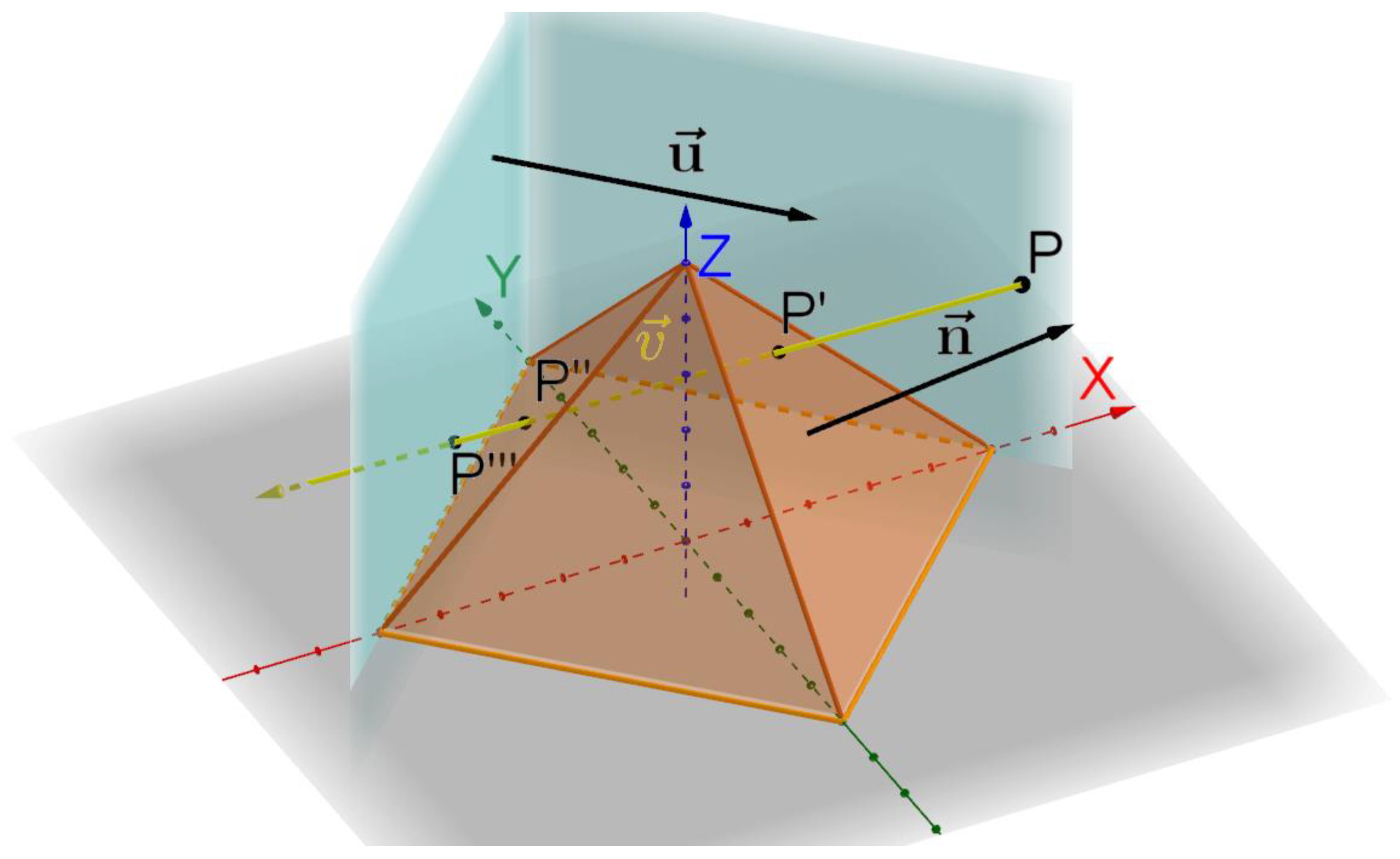
Figure 2. Interaction of the ray with a textured Si pyramid. Starting from the initial point P, the ray direction v intersects the pyramid at the points P′ and P″ as well as the boundary of the unit cell at P‴. The closest point to P is P′, which will be selected for the next step of the algorithm. n and u are the unit vectors perpendicular to the face of the pyramid and the unit cell, respectively.
Energies 16 04292 g002
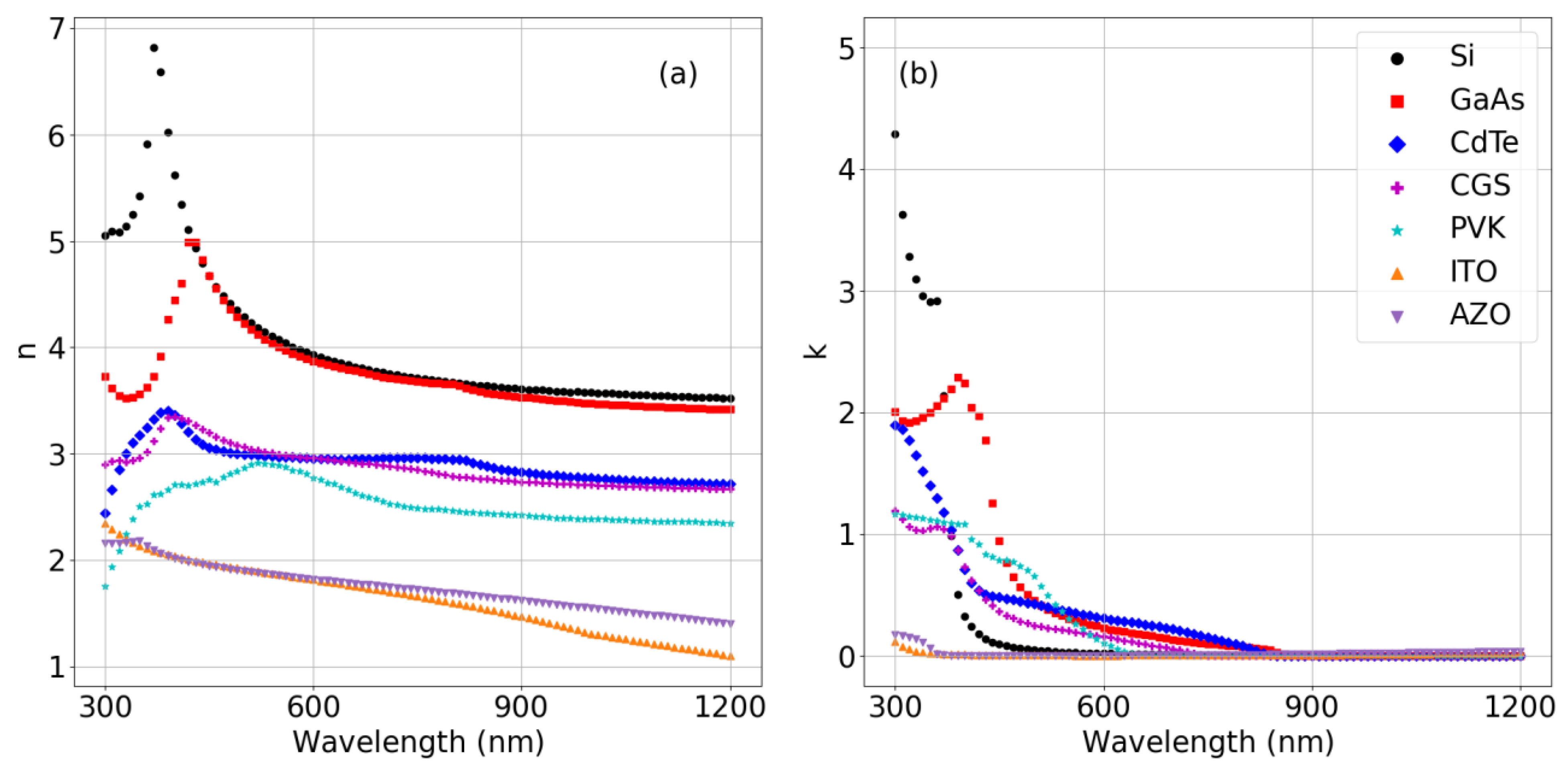
The refractive indices of the materials considered in this work can be found in [7,18,19,20,21,22] and are reported in Figure 3.
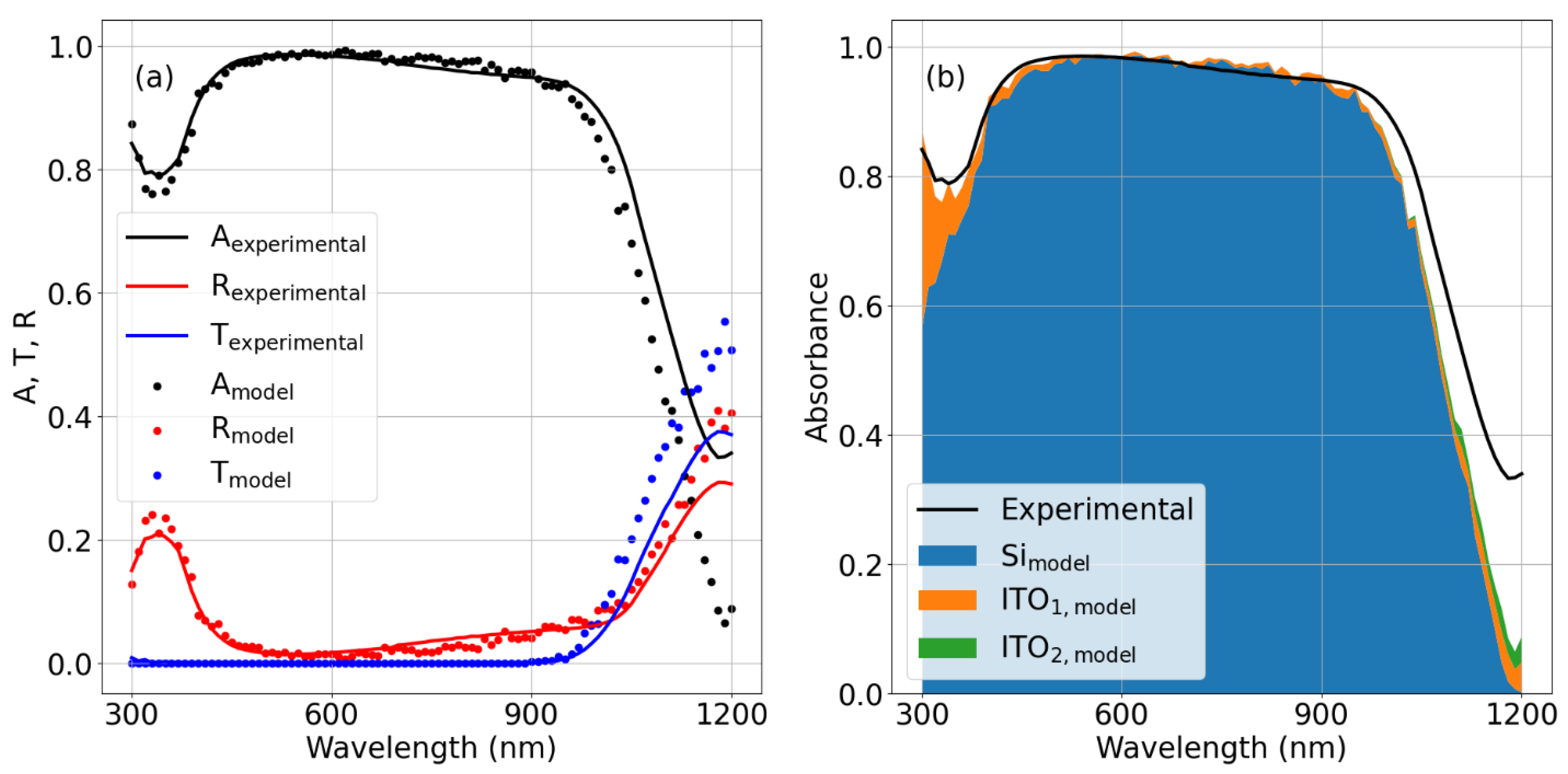
To verify the optical model, we tested it by considering a textured 160 μm silicon sample covered with ITO1 (80 nm) and ITO2 (100 nm), manufactured by Enel Green Power. Experimental data of reflectivity and transmissivity taken with a Bentham PVE300 for this structure were compared to the reflectivity and transmissivity spectra calculated through the present model. The results, reported in Figure 4, show that good agreement between the model and experimental data was found (Figure 4a), thus confirming the good accuracy of the proposed model, as well as the contribution of each layer in the sample system to the total absorbance (Figure 4b). More relevant deviations between model and data were found in the near-infrared region around 1000 nm, where an underestimate of absorbance was found. Such deviation is most likely due to relevant scattering effects occurring when the wavelength is close to the pyramid feature size, which cannot be accurately modeled using ray tracing, as shown in [23].

3. Electrical Model

The fractions of reflected, transmitted and absorbed rays determine the reflectivity R ( λ ) , the transmittivity T ( λ ) of the multi-junction module and the absorbance A j ( λ ) of each layer. Then, the short-circuit current ( I s c ) of each sub-module is calculated as
I s c = q S A s ( λ ) · ϕ ( λ ) · d λ
where q is the electron charge, S is the cell area, A s ( λ ) is the semiconductor absorbance and ϕ ( λ ) is the photon flux. The ideal I–V characteristics of the sub-module are determined by the lumped element model:
I ( V ) = I s c I 0 ( e q V k b T 1 )
with I 0 being the dark saturation current, k b being the Boltzmann constant and T being the temperature of the sub-module. To evaluate the performance of the multi-junction module in standard test conditions (STC), ϕ ( λ ) is the photon flux of the standard ASTM G-173-03 solar spectrum [24] and T = 25 °C.
To evaluate I 0 we considered the Shockley–Queisser (SQ) limit [25], in which non-radiative recombination phenomena are neglected and I 0 is therefore
I 0 = q 2 S Q T
where Q T is the blackbody radiation at the temperature of the cell due to radiative recombination processes; this radiation emits from both sides of the cell, explaining the geometric factor 2 S in the previous formula, as reported in the reference. Other important phenomena, including non-radiative recombination processes such as Auger recombination [26], as well as positive ones, such as photon recycling [27], are not accounted for in the case of an ideal SQ limit, but will be included heuristically in the last section of this work.
In the case of VM2T modules, different numbers of cells must be connected in series in each sub-module in order to match the voltage outputs and maximize the performance increase from the parallel connection. We considered 72 cells of M2 pseudo-square geometry [28] with a cell area SSi of 241.4 cm2 in the Si sub-module, as this is a common case in commercial modules [29], and the number of cells in the top sub-module can then be obtained using
n t o p = r o u n d ( V o c , S i · n S i V o c , T C S )
where n t o p and n S i are the number of cells connected in series and V o c , T C S and V o c , S i are the open-circuit voltages of a single cell in each sub-module, respectively. The areas of the two sub-modules are equal; therefore, the top cell area Stop is equal to 72 · S S i / n t o p . It is important to note that losses due to cell spacing in the module and the metallic grid shadowing are ignored.
Once the cell areas SSi and Stop are known, Equations (2) and (3) are used to calculate the I–V characteristics of a single cell; then, in each sub-module, the voltage in the I-V curve is multiplied by n t o p and n S i , respectively, as the cells are connected in series with the assumptions that series resistance is negligible and that all cells are exactly equal in each sub-module. Finally, the I-V curves of the two sub-modules are summed in terms of current as these are connected in parallel, and the VM2T module’s efficiency in converting solar power to electrical power is then calculated as
P C E = max ( P V M 2 T ) 72 · A S i · 1000   W / m 2
where max ( P V M 2 T ) is the maximum power point of the power–voltage characteristics of the whole VM2T module, 72 · S S i corresponds to the area of the whole module (as the two sub-modules have an equal area) and 1000 W / m 2 is the optical irradiance of the standard solar spectrum.
The advantage of our approach based on Monte Carlo ray tracing, negligible series resistances and a V o c equal to the Shockley–Queisser limit is that it requires a very limited number of parameters. Only the real and imaginary parts of the refractive index are actually required, since only the optical absorbance of the solar cells is actually evaluated. Aspects such as doping profiles, carrier lifetimes and surface recombination velocities, which are important parameters in other widely used solar cell simulation programs [30,31,32,33], are not considered in our model, since they are cumulatively incorporated by considering the open-circuit voltage of the cell, either in the Shockley–Queisser limit or, as will be discussed in more detail in the next sections, in the case of the record, current state-of-the-art solar cells.

4. Results and Discussion

4.1. VM2T Module Optimization

To optimize the thicknesses of AZO1, AZO2, ITO1 and the interlayer of the VM2T module, we considered the case of the CdTe/Si module, since the refractive index of CdTe is close to the average of all the considered semiconductors for the top module, as can be seen from Figure 3. Rather than simulating all the possible combinations of the four parameters, we optimized one layer at a time, while keeping each optimal thickness fixed in the following steps (a similar approach was employed in [34,35]). Starting from the initial configuration l A Z O 2 = 100   nm , l I T O 1 = 80   nm , l i n t e r l a y e r = 100   μ m and l C d T e = 2   μ m , we first varied the thicknesses of the TCO layers and the interlayer.
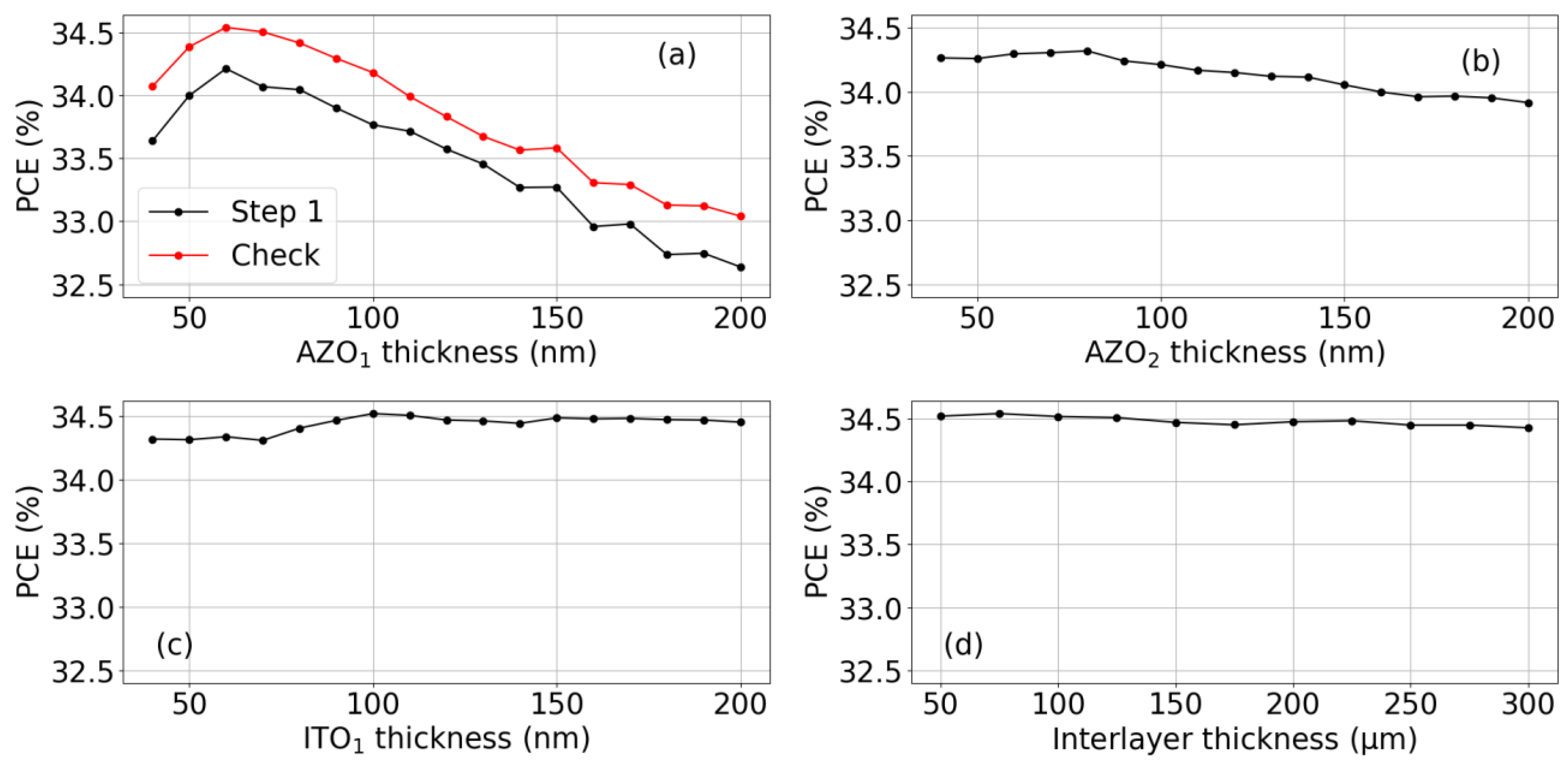
In the first step of the optimization process, the thickness of the first AZO layer was varied while the other thicknesses were fixed to the values reported above; the results shown in Figure 5a indicate that the optimal thickness of this layer is 60 nm, and this value was fixed for the following steps. In the next step, the thickness of the second AZO layer was varied to obtain an optimal value of 80 nm (Figure 5b). In the same fashion, the optimal thickness of the top ITO layer (Figure 5c) was determined to be 100 nm (similar results for the ITO layer have already been reported in [36]), and the optimal interlayer thickness was 75 µm (Figure 5d). At the end of the process, a new optimization iteration was performed on the first AZO layer to check that the optimal value had not changed due to the optimization of the following layers (Figure 5a).
It has to be noted that the order in which the layers were optimized was determined by the impact of each layer on the optics of the overall system; in fact, by comparing the scales of the y-axis of the subfigures, it can be seen that each layer had less influence on the PCE of the module than the previous one. In particular, the most relevant parameter among AZO1, AZO2, ITO1 and interlayer thicknesses was the AZO1 thickness.
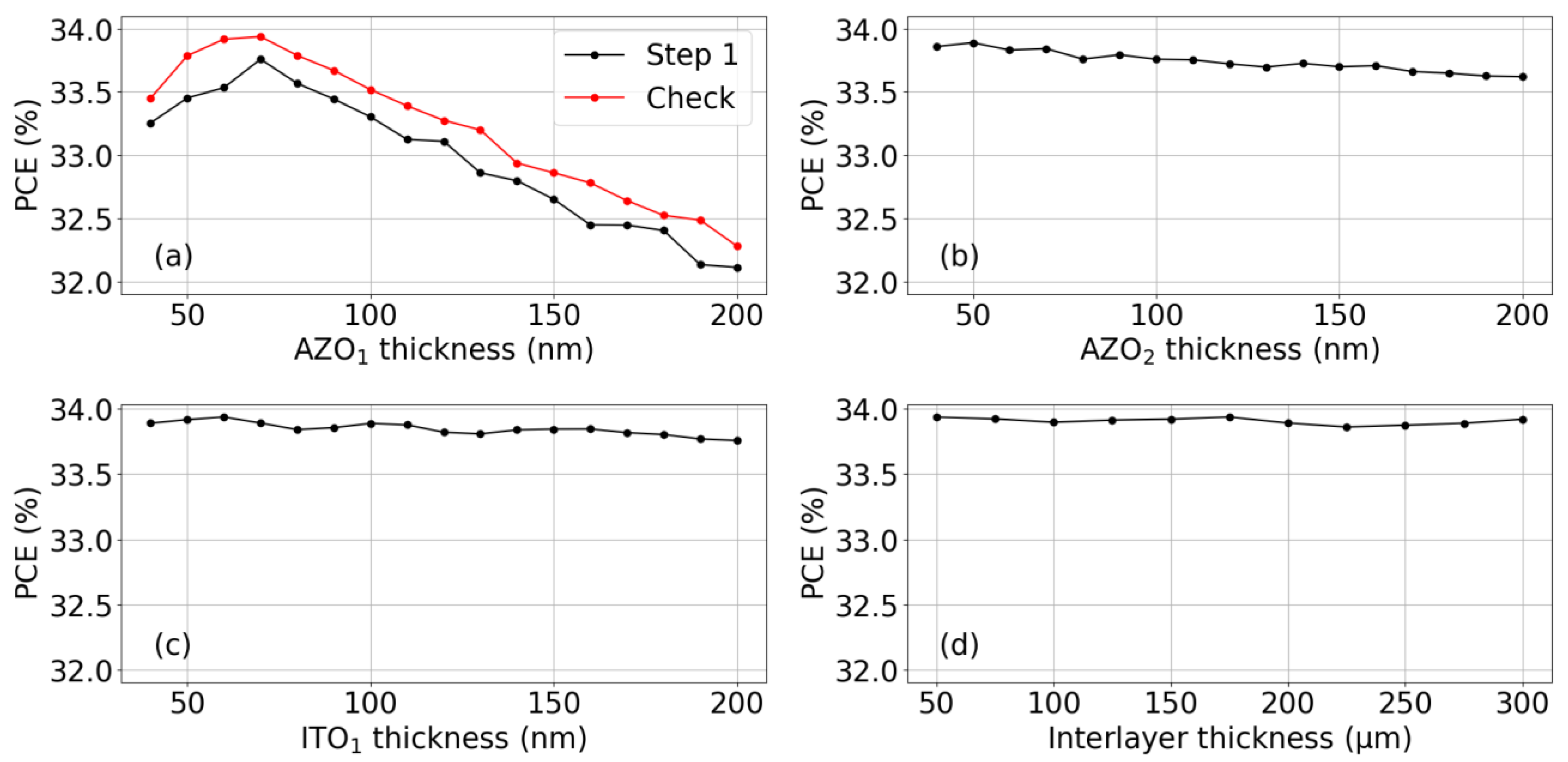
As is well known, Si texturization is widely used in PV technology to trap light by increasing the number of reflections and enhancing the optical path before light can escape the surface, therefore increasing the current output [16]. However, to facilitate the device manufacturing for the realization of a mechanically stacked 2T device and even more so in the case of a 2T tandem cell, it may be desirable to avoid Si texturization. Therefore, we evaluated the impact of texturization on the overall device performance. To this end, we considered a VM2T CdTe/Si module where the top ITO layer and the top Si surface were flat (whereas the bottom surfaces were still textured), and we optimized the system with the same procedure reported above.
The values reported In Figure 6 indicate the optimal thickness of the first AZO layer was 70 nm (Figure 6a), the optimal thickness of the second AZO layer was 50 nm (Figure 6b), the optimal thickness of the first ITO layer (which is now flat) was 60 nm (Figure 6c) and the optimal thickness of the interlayer was 175 µm (Figure 6d). Again, the first optimization step was repeated to check that the optimal value did not change during the process. As for the case of the textured Si shown in Figure 5, in this case the impact of each layer decreased at each step, with the interlayer having the smallest effect on the PCE of the module as it served no optical purpose and was mostly transparent to the wavelength range of interest.
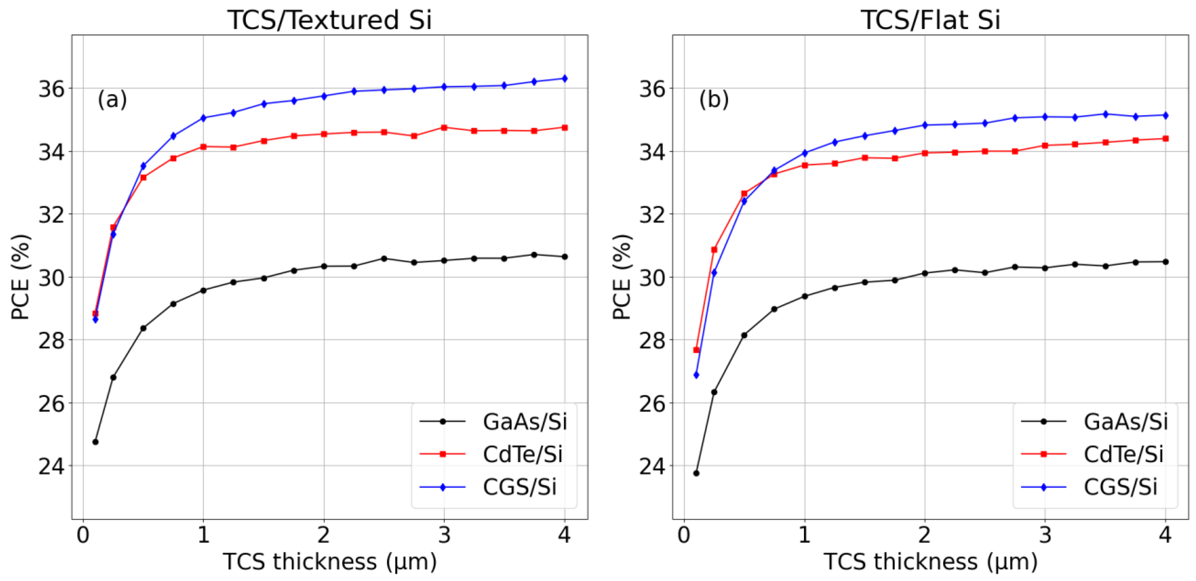
With the AZO1, AZO2, ITO1 and interlayer thicknesses optimized as shown in Figure 5 and Figure 6, it was possible to focus on the optimization of the TCS thickness. This variable was allowed to span from 0.1 µm to 4 µm, and the results are reported in Figure 7, showing the VM2T system efficiency under STC as a function of TCS thickness. From the inspection of Figure 7, it is evident that the PCE increased with the TCS thickness, though the PCE increased with respect to a decrease in thickness greater than 1 µm. Since a minority of carrier diffusion lengths in thin-film PV technologies are generally of the order 1 of μm or below [37,38], and given the change in slope at 1 µm in Figure 7, we assumed 1 µm to be the maximum realistically possible TCS thickness, as the increase in absorbance in thicker films would be balanced out by the increased recombination effects.
For reference, the SQ PCE of the single-junction Si cell, based on the absorbance, transmittivity and reflectivity values shown in Figure 3, was 28.87%. In the case of the textured Si module, the GaAs/Si module reached an SQ PCE of 30.7%, the CdTe/Si module reached an SQ PCE of 34.7% and the CGS/Si module reached an SQ PCE of 36.3%. The relative PCE loss between modules with a flat Si sub-module and a textured Si sub-module was about 3.3% for the CGS/Si module, 1% for the CdTe/Si module and 0.4% for the GaAs/Si sub-module; these differences are due to the fact that GaAs and CdTe have lower bandgap energies than CGS (1.42 eV, 1.5 eV and 1.7 eV, respectively), and therefore overlap more than the latter with the wavelength range absorbed by the Si sub-module, reducing the contribution of the Si bottom sub-module to the performance of the system.

4.2. VM2T PVK/Si Module Analysis

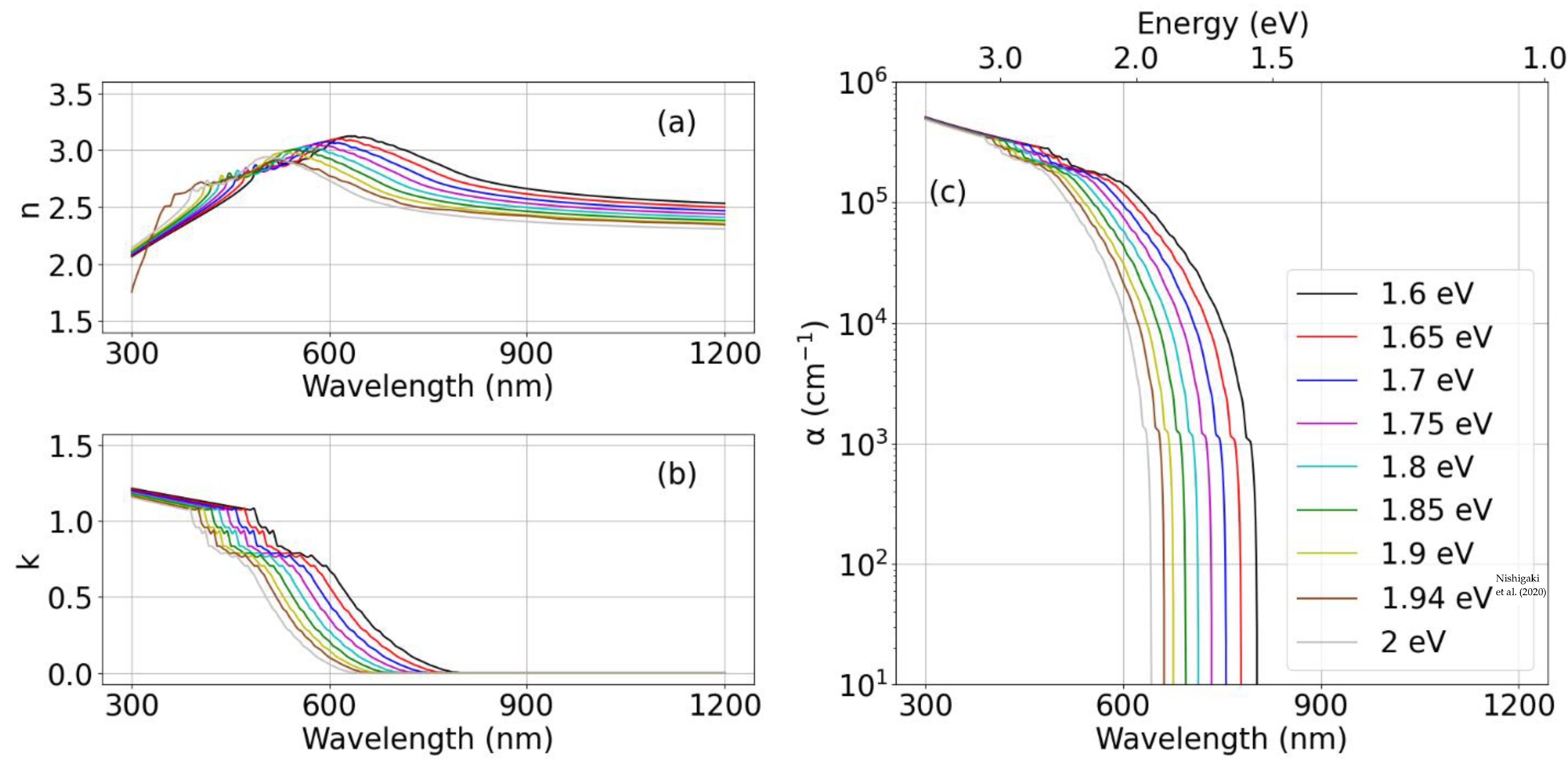
One important advantage of PVK is the feasibility of tuning its bandgap [39]. It is therefore useful to evaluate the optical PVK bandgap for the coupling with Si. In order to estimate the performance of PVK/Si modules with different PVK bandgaps, we started by considering the experimental optical constants of PVK with a bandgap of 1.94 eV [7]. We then modified the imaginary part of the refractive index to obtain bandgaps ranging from 1.6 eV to 2 eV, and recalculated the real part through the Kramers–Kronig relations [40]. The new refractive indices are reported in Figure 8a,b, along with the absorption coefficient α (Figure 8c).
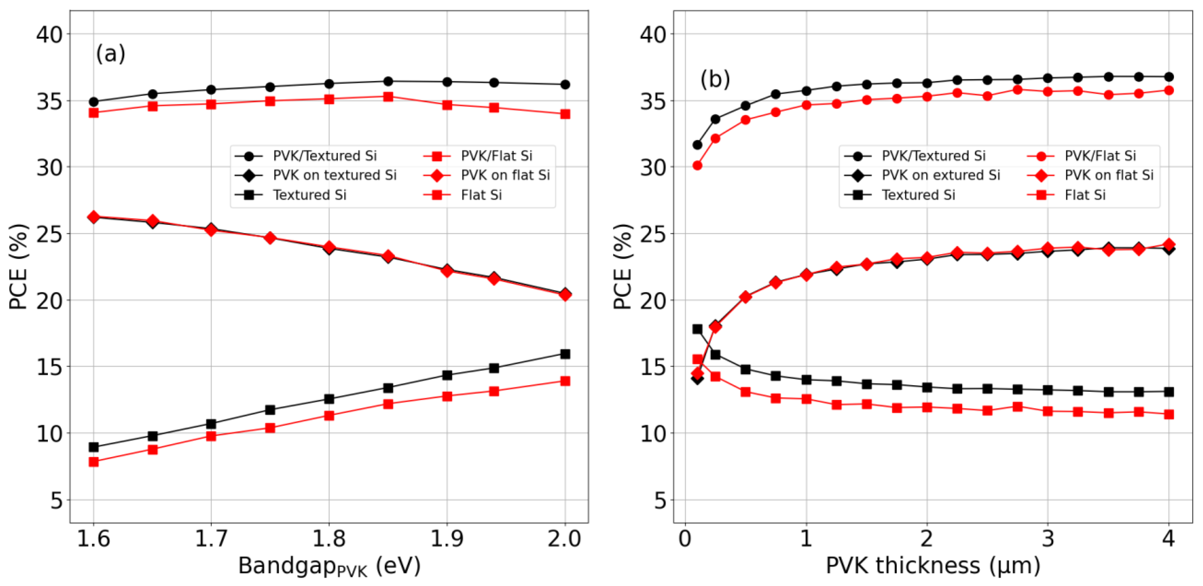
With the optimized thicknesses of AZO1, AZO2, ITO1 and the interlayer reported in the previous section, we varied the PVK bandgap energy from 1.6 eV to 2 eV (with a fixed thickness of 2 µm) for the cases of the textured Si module and the flat Si module. Figure 9 reports the results of these calculations. In Figure 9a, it can be observed that in both cases, the optimal bandgap energy was 1.85 eV, which is quite different from the value commonly reported in the literature of 1.7 eV [41]. However, this value is usually obtained through ab initio calculations, where the absorbances of the materials are assumed to be one, neglecting optical effects altogether. On the contrary, the simulations showed that an accurate evaluation of the performance of a photovoltaic system must include an optical model that considers the refractive indices of all materials involved. Moreover, it has to be noted that the difference in PCE between the modules with textured and flat Si surfaces increased with the PVK bandgap energy, in accordance with what was stated in the previous section; in fact, it can be seen that PVK’s contribution to the overall PCE decreased with an increasing bandgap, whereas the contribution of Si (and of its texture) increased.
By varying the semiconductor thickness for the 1.85 eV bandgap PVK, it can be seen from Figure 9b that the PVK/textured Si module reached an SQ PCE value of 36.7% with a relative 3% decrease in the case of the PVK/flat Si module.

5. State-of-the-Art Module Efficiencies

As mentioned in Section 3, the PCE of the multi-junction modules was calculated in the SQ condition. However, the SQ limit is an ideal condition, in which recombination is assumed to be minimal. During the development of PV technology, different semiconductor technologies have been experimented with, and they have achieved different levels of performance compared to the maximum achievable according to their respective SQ theoretical limit [42]. Such differences are due to various loss mechanisms, such as Shockley–Read–Hall, Auger and surface recombination, which increase I 0 and limit the voltage output of the solar cell. In general, the weights of these phenomena depend on the semiconductor used as well as the cell design. For this reason, in order to provide a more realistic estimate of achievable multi-junction module efficiency, we introduced a technology development coefficient (TDC), defined as the ratio between the open-circuit voltages of state-of-the-art (SA) cells and the ideal SQ limit for the same semiconductor evaluated in STC. This coefficient was introduced to take into account all the recombination processes (Auger, Shockley–Read–Hall, interfaces, photon recycling, etc.) even without an accurate electrical model. As SA values, we considered those reported in [43], while the SQ values were obtained by considering the voltage of the ideal I–V characteristics of (2) at I = 0   A . The TDCs for the semiconductor technologies considered in this work are reported in Table 1. It must be noted that, although for CIGS and perovskite the materials employed for the record cells reported in the literature have different bandgap energies compared to those considered within this work, we assumed the same value for the TDC.
Once the TDC of each semiconductor was calculated, when calculating the I–V characteristics of each sub-module, an initial SQ calculation was performed. Then, the dark saturation current was updated as
I 0 = I s c e q · V o c · T D C k b T 1
Then, the I–V characteristics of the sub-modules were recalculated as well as the parallel connection between the two.
We report in Table 2 the efficiencies for the VM2T modules with textured Si obtained in the SQ limit and considering the TDC of each semiconductor. The number of cells in the top sub-module was modified to take into account the lower voltage output of the state-of-the-art cells compared to their theoretical limit, whereas the number of Si cells in the bottom sub-module was fixed at 72. The number of cells connected in series in the top sub-module depended on the ratio between the SA V o c values of the TCS and Si and therefore on each TDC.
The PCE drop was more noticeable in the CdTe/Si module as CdTe has the lowest TDC, whereas the drop was much lower in the GaAs/Si module as GaAs has the highest TDC.
From Table 2, it is clear that GaAs and CGS reached about 30% efficiency, while CdTe only reached about 25%. This is due to CdTe’s lower TDC compared to the other technologies, but this may change substantially as CdTe technology progresses.
Among all the considered top semiconductors, the PVK module with the 1.85 eV bandgap was the one allowing, in principle, the best VM2T PV system efficiency, which reached about 34%, about 13% more than the other semiconductors.

6. Conclusions

In this work, we developed an optical model for VM2T PV systems based on Monte Carlo ray tracing. The model was specifically designed for textured surfaces such as the pyramidal texture of Si solar cells thanks to the unit cell approach, which allows accurate simulation of infinite textured surfaces. Moreover, contrarily to most ray-tracing algorithms, no limit is imposed on the maximum optical path of rays. The model was applied to evaluate the PCE of four multi-junction modules: GaAs/Si, CdTe/Si, CGS/Si and PVK/Si. The system was first optimized by tuning the thicknesses of the top sub-module in the VM2T CdTe/Si module, starting from the most impactful layers. The optimized VM2T setup was tested with the other semiconductor combinations in order to determine their potential in the VM2T configuration, obtaining a maximum PCE within the Shockley–Queisser limit of 36.07% for the CGS/Si module, 34.53% for the CdTe/Si module and 30.51% for the GaAs/Si module.
We also evaluated the same VM2T modules in a system in which the top surface of the Si layer and the overlying ITO layer were flat, obtaining a decrease in PCE, though this increased with the bandgap energy of the top semiconductor, ranging from 0.4% to 3.3%.
As for the PVK/Si module, since it is possible to accurately tune PVK’s bandgap energy, a first set of simulations was performed by modifying the refractive index of the material through the Kramers–Kronig relations for different bandgap energies. We determined that the optimal bandgap energy for Si-based multi-junction modules is 1.85 eV. With this PVK, the highest PCE value achieved within the Shockley–Queisser limit was 36.77%.
Lastly, in order to provide insight into realistic performances based on state-of-the-art technology rather than on theoretical limits, we introduced a technology development coefficient, defined as the ratio between the open-circuit voltage of the top efficiency cell and the one calculated in the Shockley–Queisser limit, and we calculated the performance of the modules by taking into account the updated dark saturation current. For the VM2T GaAs/Si, CdTe/Si, CGS/Si and PVK/Si modules, we obtained a PCE of 29.45%, 25.24%, 31.74% and 34.16%, respectively.

Author Contributions

R.C.: Methodology, Software, Formal Analysis, Investigation, Data Curation, Writing—Original Draft, Visualization. M.L.: Methodology, Investigation. R.G.M.: Methodology. A.S.: Methodology. S.M.S.P.: Supervision. M.F.: Resources. C.G.: Resources. S.A.L.: Conceptualization, Methodology, Validation, Writing—Review and Editing, Supervision, Project Administration, Funding Acquisition. All authors have read and agreed to the published version of the manuscript.

Funding

This research was in part funded by Italian MUR, PON Ricerca e Innovazione 2014–2020, under the Decreto Direttoriale di concessione dell’agevolazione del 21 May 2019 prot. n. 991, contract code ARS01_00519, BEST-4U Project and the Research Infrastructure “Beyond-Nano” co-funded by Regione Sicilia (D.D.G. 2929/5S) and by the Italian Ministry of University and Research (Decree 2510/2019).

Data Availability Statement

The data presented in this study are available on request from the corresponding author.

Conflicts of Interest

The authors declare that they have no known competing financial interests or personal relationships that could have appeared to influence the work reported in this paper.

References

  1. Fraunhofer Institute for Solar Energy Systems, ISE; PSE Projects GmbH. Photovoltaics Report (fraunhofer.de). Available online: https://www.ise.fraunhofer.de/content/dam/ise/de/documents/publications/studies/Photovoltaics-Report.pdf (accessed on 21 October 2022).
  2. Yu, Z.J.; Fisher, K.C.; Holman, Z.C. Evaluation of spectrum-splitting dichroic mirrors for PV mirror tandem solar cells. In Proceedings of the 2015 IEEE 42nd Photovoltaic Specialist Conference (PVSC), New Orleans, LA, USA, 14–19 June 2015. [Google Scholar] [CrossRef]
  3. Werner, J.; Niesen, B.; Ballif, C. Perovskite/Silicon Tandem Solar Cells: Marriage of Convenience or True Love Story?—An Overview. Adv. Mater. Interfaces 2018, 5, 1700731. [Google Scholar] [CrossRef]
  4. Wu, Y.; Kostuk, R.K. Two-junction holographic spectrum-splitting microconcentrating photovoltaic system. J. Photonics Energy 2017, 7, 17001. [Google Scholar] [CrossRef]
  5. Scuto, A.; Corso, R.; Leonardi, M.; Milazzo, R.G.; Privitera, S.M.S.; Colletti, C.; Foti, M.; Bizzarri, F.; Gerardi, C.; Lombardo, S.A. Outdoor performance of GaAs/bifacial Si heterojunction four-terminal system using optical spectrum splitting. Sol. Energy 2022, 241, 483–491. [Google Scholar] [CrossRef]
  6. Saleh, B.E.; Teich, M.C. Fundamentals of Photonics; John Wiley & Sons: Hoboken, NJ, USA, 2019. [Google Scholar]
  7. Nishigaki, Y.; Nagai, T.; Nishiwaki, M.; Aizawa, T.; Kozawa, M.; Hanzawa, K.; Kato, Y.; Sai, H.; Hiramatsu, H.; Hosono, H.; et al. Extraordinary strong band-edge absorption in distorted chalcogenide perovskites. Sol. RRL 2020, 4, 1900555. [Google Scholar] [CrossRef]
  8. Fashina, A.; Kana, M.G.Z.; Soboyejo, W.O. Optical reflectance of alkali-textured silicon wafers with pyramidal facets: 2D analytical model. J. Mater. Res. 2015, 30, 904–913. [Google Scholar] [CrossRef]
  9. Chen, Q.; Liu, Y.; Wang, Y.; Chen, W.; Wu, J.; Zhao, Y.; Du, X. Optical properties of a random inverted pyramid textured silicon surface studied by the ray tracing method. Sol. Energy 2019, 186, 392–397. [Google Scholar] [CrossRef]
  10. Reiners, N.; Blieske, U. SMARTI—An Open Source Matlab Ray Tracing Tool for Solar Cell and Module Optics. In Proceedings of the 2018 7th International Energy and Sustainability Conference (IESC), Cologne, Germany, 17–18 May 2018. [Google Scholar] [CrossRef]
  11. Holst, H.; Winter, M.; Vogt, M.R.; Bothe, K.; Köntges, M.; Brendel, R.; Altermatt, P.P. Application of a New Ray Tracing Framework to the Analysis of Extended Regions in Si Solar Cell Modules. Energy Procedia 2013, 38, 86–93. [Google Scholar] [CrossRef]
  12. Rafiee, M.; Ahmed, H.; Chandra, S.; Sethi, A.; McCormack, S.J. Monte Carlo ray tracing modelling of multi-crystalline silicon photovoltaic device enhanced by luminescent material. In Proceedings of the 2018 IEEE 7th World Conference on Photovoltaic Energy Conversion (WCPEC) (A Joint Conference of 45th IEEE PVSC, 28th PVSEC & 34th EU PVSEC), Waikoloa, HI, USA, 10–15 June 2018. [Google Scholar]
  13. LIGHTHOUSE. Wafer Ray Tracer (pvlighthouse.com.au). Available online: https://www2.pvlighthouse.com.au/calculators/wafer%20ray%20tracer/wafer%20ray%20tracer.html (accessed on 14 April 2023).
  14. Essig, S.; Allebé, C.; Remo, T.; Geisz, J.F.; Steiner, M.A.; Horowitz, K.; Barraud, L.; Ward, J.S.; Schnabel, M.; Descoeudres, A.; et al. Raising the one-sun conversion efficiency of III–V/Si solar cells to 32.8% for two junctions and 35.9% for three junctions. Nat. Energy 2017, 2, 1–9. [Google Scholar] [CrossRef]
  15. Schulze, P.S.C.; Bett, A.J.; Bivour, M.; Caprioglio, P.; Gerspacher, F.M.; Kabaklı, Ö.Ş.; Richter, A.; Stolterfoht, M.; Zhang, Q.; Neher, D.; et al. 25.1% High-Efficiency Monolithic Perovskite Silicon Tandem Solar Cell with a High Bandgap Perovskite Absorber. Sol. RRL 2020, 4, 2000152. [Google Scholar] [CrossRef]
  16. Campbell, P.; Green, M.A. Light trapping properties of pyramidally textured surfaces. J. Appl. Phys. 1987, 62, 243–249. [Google Scholar] [CrossRef]
  17. De Greve, B. Reflections and refractions in ray tracing. Retrived Oct. 2006, 16, 2014. [Google Scholar]
  18. Green, M.A. Self-consistent optical parameters of intrinsic silicon at 300K including temperature coefficients. Sol. Energy Mater. Sol. Cells 2008, 92, 1305–1310. [Google Scholar] [CrossRef]
  19. Papatryfonos, K.; Angelova, T.; Brimont, A.; Reid, B.; Guldin, S.; Smith, P.R.; Tang, M.; Li, K.; Seeds, A.J.; Liu, H.; et al. Refractive indices of MBE-grown AlxGa (1 − x) As ternary alloys in the transparent wavelength region. AIP Adv. 2021, 11, 025327. [Google Scholar] [CrossRef]
  20. E Treharne, R.; Seymour-Pierce, A.; DuRose, K.; Hutchings, K.; Roncallo, S.; Lane, D. Optical Design and Fabrication of Fully Sputtered CdTe/CdS Solar Cells. J. Phys. Conf. Ser. 2011, 286, 012038. [Google Scholar] [CrossRef]
  21. Leem, J.W.; Yu, J.S. Influence of oblique-angle sputtered transparent conducting oxides on performance of Si-based thin film solar cells. Phys. Status Solidi (a) 2011, 208, 2220–2225. [Google Scholar] [CrossRef]
  22. Minoura, S.; Maekawa, T.; Kodera, K.; Nakane, A.; Niki, S.; Fujiwara, H. Optical constants of Cu (In, Ga) Se2 for arbitrary Cu and Ga compositions. J. Appl. Phys. 2015, 117, 195703. [Google Scholar] [CrossRef]
  23. Höhn, O.; Tucher, N.; Bläsi, B. Theoretical study of pyramid sizes and scattering effects in silicon photovoltaic module stacks. Opt. Express 2018, 26, A320–A330. [Google Scholar] [CrossRef]
  24. Standard Tables for Reference Solar Spectral Irradiances: Direct Normal and Hemispherical on 37° Tilted Surface (astm.org). Available online: https://www.astm.org/g0173-03r20.html (accessed on 22 December 2022).
  25. Shockley, W.; Queisser, H.J. Detailed Balance Limit of Efficiency of p-n Junction Solar Cells. J. Appl. Phys. 1961, 32, 510–519. [Google Scholar] [CrossRef]
  26. Richter, A.; Werner, F.; Cuevas, A.; Schmidt, J.; Glunz, S. Improved Parameterization of Auger Recombination in Silicon. Energy Procedia 2012, 27, 88–94. [Google Scholar] [CrossRef]
  27. Raja, W.; De Bastiani, M.; Allen, T.G.; Aydin, E.; Razzaq, A.; Rehman, A.U.; Ugur, E.; Babayigit, A.; Subbiah, A.S.; Isikgor, F.H.; et al. Photon recycling in perovskite solar cells and its impact on device design. Nanophotonics 2021, 10, 2023–2042. [Google Scholar] [CrossRef]
  28. Linss, V.; Dietsch, T.; Baumann, J.; Graupner, U.; Hoß, J.; Linke, J.; Lossen, J.; Polzin, J.I.; Mack, S.; Nagel, H.; et al. Single Sided High Throughput Sputter Process Technology for In-Situ Doped n-Type Amorphous Silicon Layers for High Efficiency TOPCon Solar Cells. In Proceedings of the 39th European Photovoltaic Solar Energy Conference and Exhibition, Milan, Italy, 26–30 September 2022; pp. 202–207. [Google Scholar]
  29. Monokroussos, C.; Salis, E.; Etienne, D.; Zhang, X.; Dittmann, S.; Friesen, G.; Morita, K.; Stang, J.; Herbrecht, T.; Fakhfouri, V.; et al. Electrical characterization intercomparison of high-efficiency c-Si modules within Asian and European laboratories. Prog. Photovolt. Res. Appl. 2019, 27, 603–622. [Google Scholar] [CrossRef]
  30. Basore, P.A. Multidimensional Fourier-Series Solution of the Quasi-Neutral Drift–Diffusion Equations. IEEE J. Photovolt. 2020, 10, 905–911. [Google Scholar] [CrossRef]
  31. Fell, A.; Fong, K.C.; McIntosh, K.R.; Franklin, E.; Blakers, A.W. 3-D Simulation of Interdigitated-Back-Contact Silicon Solar Cells With Quokka Including Perimeter Losses. IEEE J. Photovolt. 2014, 4, 1040–1045. [Google Scholar] [CrossRef]
  32. Varache, R.; Leendertz, C.; Gueunier-Farret, M.; Haschke, J.; Muñoz, D.; Korte, L. Investigation of selective junctions using a newly developed tunnel current model for solar cell applications. Sol. Energy Mater. Sol. Cells 2015, 141, 14–23. [Google Scholar] [CrossRef]
  33. Liu, Y.; Ahmadpour, M.; Adam, J.; Kjelstrup-Hansen, J.; Rubahn, H.-G.; Madsen, M. Modeling Multijunction Solar Cells by Nonlocal Tunneling and Subcell Analysis. IEEE J. Photovolt. 2018, 8, 1363–1369. [Google Scholar] [CrossRef]
  34. Jhuma, F.A.; Shaily, M.Z.; Rashid, M.J. Towards high-efficiency CZTS solar cell through buffer layer optimization. Mater. Renew. Sustain. Energy 2019, 8, 6. [Google Scholar] [CrossRef]
  35. Yaşar, S.; Kahraman, S.; Çetinkaya, S.; Apaydın, Ş.; Bilican, I.; Uluer, I. Numerical thickness optimization study of CIGS based solar cells with wxAMPS. Optik 2016, 127, 8827–8835. [Google Scholar] [CrossRef]
  36. Canino, M.; Boldrini, V.; Rizzoli, R.; Centurioni, E.; Maurizi, A.; Lombardo, S.; Terrasi, A.; Summonte, C. TCO Optimization of c-Si Heterojunction Solar Cells for Tandem Architecture by Optical Simulation. In Proceedings of the 38th European Photovoltaic Solar Energy Conference and Exhibition, Online, 6–10 September 2021; pp. 501–504. [Google Scholar] [CrossRef]
  37. Yoon, H.P.; Haney, P.M.; Yoon, Y.; An, S.; Basham, J.I.; Zhitenev, N.B. Local photocarrier dynamics in CdTe solar cells under optical and electron beam excitations. In Proceedings of the 2015 IEEE 42nd Photovoltaic Specialist Conference (PVSC), New Orleans, LA, USA, 14–19 June 2015. [Google Scholar]
  38. Brown, G.; Faifer, V.; Pudov, A.; Anikeev, S.; Bykov, E.; Contreras, M.; Wu, J. Determination of the minority carrier diffusion length in compositionally graded Cu(In,Ga)Se2 solar cells using electron beam induced current. Appl. Phys. Lett. 2010, 96, 022104. [Google Scholar] [CrossRef]
  39. Hu, Z.; Lin, Z.; Su, J.; Zhang, J.; Chang, J.; Hao, Y. A review on energy band-gap engineering for perovskite photovoltaics. Sol. RRL 2019, 3, 1900304. [Google Scholar] [CrossRef]
  40. Lucarini, V.; Saarinen, J.J.; Peiponen, K.E.; Vartiainen, E.M. Kramers-Kronig Relations in Optical Materials Research; Springer Science & Business Media: Berlin/Heidelberg, Germany, 2005; Volume 110. [Google Scholar]
  41. Yu, Z.J.; Leilaeioun, M.; Holman, Z. Selecting tandem partners for silicon solar cells. Nat. Energy 2016, 1, 16137. [Google Scholar] [CrossRef]
  42. Li, X.; Xu, Q.; Yan, L.; Ren, C.; Shi, B.; Wang, P.; Mazumdar, S.; Hou, G.; Zhao, Y.; Zhang, X. Silicon heterojunction-based tandem solar cells: Past, status, and future prospects. Nanophotonics 2020, 10, 2001–2022. [Google Scholar] [CrossRef]
  43. Green, M.A.; Dunlop, E.D.; Hohl-Ebinger, J.; Yoshita, M.; Kopidakis, N.; Bothe, K.; Hinken, D.; Rauer, M.; Hao, X. Solar cell efficiency tables (Version 60). Prog. Photovolt. Res. Appl. 2022, 30, 687–701. [Google Scholar] [CrossRef]
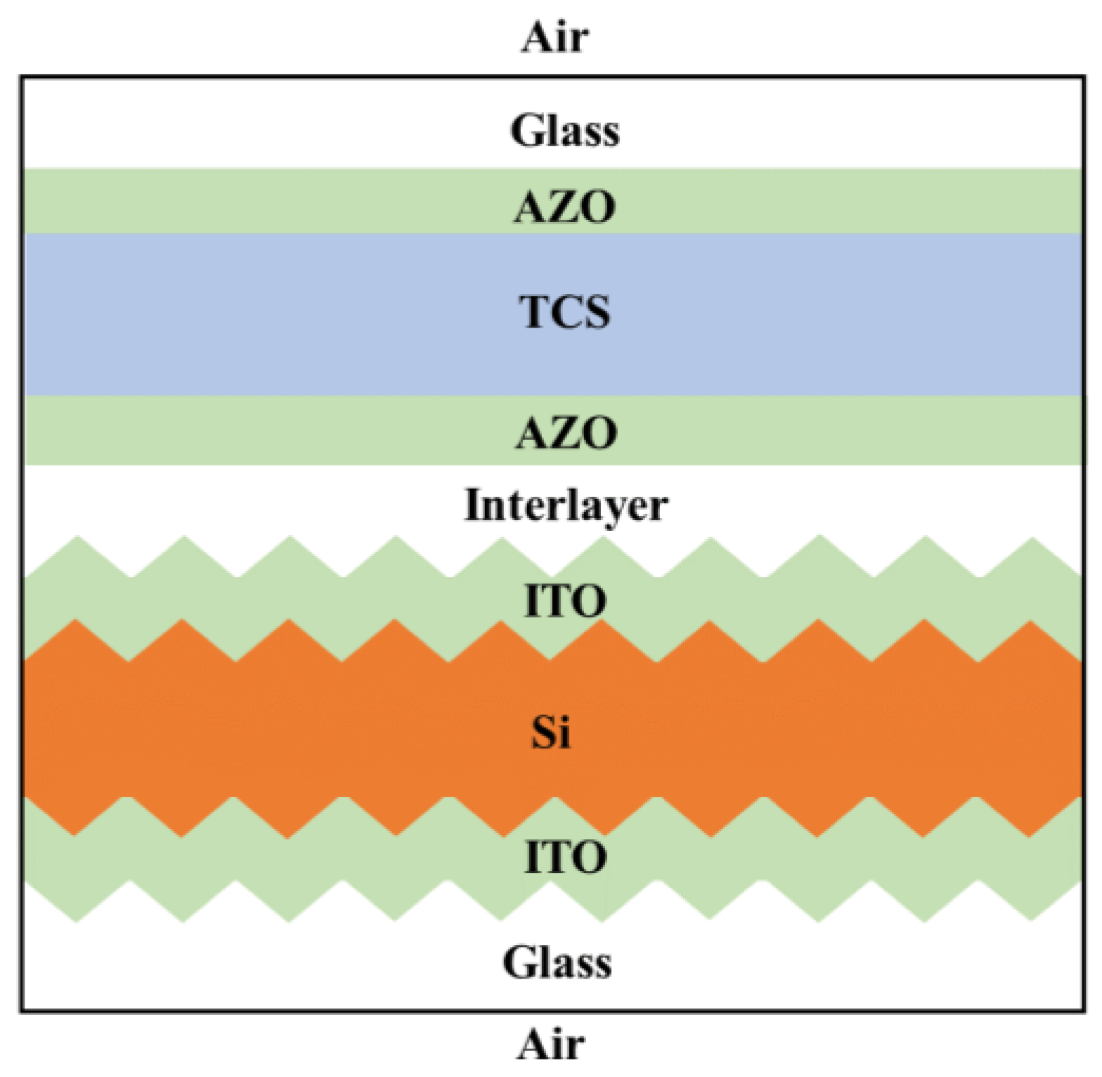
Figure 1. Layers of the VM2T multi-junction module. The top sub-module is flat, whereas the Si and ITO layers of the bottom sub-module are textured.
Energies 16 04292 g001
Figure 3. Real (a) and complex (b) parts of the complex refractive indices of the materials considered in this work as reported in [7,18,19,20,21,22]. Legend applies to both subfigures.
Energies 16 04292 g003
Figure 4. Comparison between experimental and simulated absorbances, reflectances and transmittances of an ITO/c-Si/ITO cell (a). Stacked area chart of the simulated absorbances of each layer in the test sample (b).
Energies 16 04292 g004
Figure 5. Optimization of the TCO layers and interlayer in the CdTe/Si module. The figure reports the SQ PCEs obtained by varying the thickness of the first AZO layer (a), the second AZO layer (b), the first ITO layer (c) and the interlayer (d).
Energies 16 04292 g005
Figure 6. Optimization of the TCO layers and interlayer in the CdTe/Si module with flat ITO and Si top surfaces. The figure reports the SQ PCEs obtained by varying the thickness of the first AZO layer (a), the second AZO layer (b), the first ITO layer (c) and the interlayer (d).
Energies 16 04292 g006
Figure 7. SQ PCEs of the GaAs/Si, CdTe/Si and CGS/Si VM2T modules with textured Si sub-module (a) and flat Si sub-module (b).
Energies 16 04292 g007
Figure 8. Real (a) and imaginary (b) parts of the refractive indices of PVK for bandgaps ranging from 1.6 eV to 2 eV obtained from Kramers–Kronig relations. Absorption coefficients (c) of PVK for the same bandgaps [7]. Values relative to the literature material are included for comparison. The legend applies to all sub-figures.
Energies 16 04292 g008
Figure 9. PCE as a function of PVK bandgap at the SQ limit for the VM2T PVK/textured Si and the VM2T PVK/flat Si module at a fixed PVK thickness of 2 µm (a). SQ PCE of the PVK/textured Si module and the PVK/flat Si module and each sub-module for different thicknesses of the 1.85 eV bandgap PVK (b). TCO layers and interlayer thicknesses were fixed to the values obtained from the optimization processes for multi-junction modules with textured and flat Si surfaces in Section 4.1.
Energies 16 04292 g009
Table 1. Bandgap energies, open-circuit voltages and technology development coefficients (TDCs) of the semiconductors considered in this work. For CGS and PVK, the bandgap of the record cells reported in the literature are also listed. It must be noted that for these materials, TDC calculations were based on the bandgap and voltages of the literature material, while the coefficient was assumed to be the same for the bandgap considered in this work.
SemiconductorBandgapthis work (eV)Bandgapliterature (eV)VOC,SA (V)VOC,SQ (V)TDC
Si1.12-0.7380.8600.858
GaAs1.42-1.12721.1440.985
CdTe1.5-0.8751.2150.720
CuIn1-xGaxSe21.7 (x = 1)1.080.7340.8220.893
PVK1.851.671.2131.3740.883
Table 2. Comparison between number of TCS cells and PCEs obtained in the SQ limit and for state-of-the-art cells for the VM2T modules with textured Si. PCEs of each TCS single-junction record cell as reported in [43] are included.
Module n T C S , S Q n T C S , S A PCETCS,SA (%)PCEVM2T,SQ (%)PCEVM2T,SA (%)
GaAs/Si504429.130.5129.45
CdTe/Si485721.034.5325.24
CGS/Si424023.3536.0731.74
PVK/Si383723.736.7734.16
Disclaimer/Publisher’s Note: The statements, opinions and data contained in all publications are solely those of the individual author(s) and contributor(s) and not of MDPI and/or the editor(s). MDPI and/or the editor(s) disclaim responsibility for any injury to people or property resulting from any ideas, methods, instructions or products referred to in the content.