Article

Reliability Assessment of SiC-Based Depot Charging Infrastructure with Smart and Bidirectional (V2X) Charging Strategies for Electric Buses

1
MOBI-EPOWERS Research Group, ETEC Department, Vrije Universiteit Brussel (VUB), Pleinlaan 2, 1050 Brussel, Belgium
2
Flanders Make, Gaston Geenslaan 8, 3001 Heverlee, Belgium
*
Authors to whom correspondence should be addressed.
Energies 2023, 16(1), 153; https://doi.org/10.3390/en16010153
Submission received: 29 November 2022 / Revised: 16 December 2022 / Accepted: 20 December 2022 / Published: 23 December 2022
(This article belongs to the Special Issue Design, Simulations, and Reliability of Power Converter)

Abstract

:
Nowadays, the implementation of smart charging concepts and management strategies with vehicle-to-everything (V2X) functionalities, is required to address the increasing number of battery electric buses (BEBs) in cities. However, the introduction of these new functionalities to the charging systems might affect the lifetime of the charging infrastructure. This has not been investigated yet, although it is an important aspect for the BEB operators. Therefore, this paper performs a detailed reliability assessment to study the impact of smart and bidirectional (V2X) charging on the lifetime of SiC-based high-power off-board charging infrastructure used for BEBs in a depot for overnight charging. In this paper, four different charging current profiles, generated by a smart charging algorithm, are considered. In addition, an electro-thermal model of the charging system is developed to accurately estimate the junction temperature of the switching devices when subjected to the applied charging current profiles. The thermal stress is converted into a number of cycles to failures and accumulated damage by means of a rainflow cycle counting algorithm, a lifetime model and Miner’s damage rule. Finally, a Monte Carlo analysis and a Weibull probability function fit are applied to obtain the system reliability. The results have demonstrated that smart charging strategies can improve the lifetime of the charging system by at least a factor of three compared to conventional uncoordinated charging. Moreover, an uncoordinated charging strategy fails to fulfill the lifetime requirements in the parts per million range, while bidirectional charging could even further enhance the lifetime with a factor of one and a half.

1. Introduction

In European cities, battery electric buses (BEBs) are gaining a lot of attraction due to their ability to cut air pollution and combat climate change. With 22% of the newly registered urban buses in 2021 being electric, coming from 16% in 2020, BEBs witness the largest uptake of all vehicles. If this trend continues, it is expected that public transport operators (PTOs) will only go for BEBs (or a zero-emission alternative) by 2029 at the latest [1]. Nevertheless, there are still some important challenges that need to be addressed before PTOs can reach a mass adoption of BEBs.
One of the most important factors for PTOs is the lifetime of the powertrain components of the BEBs. Therefore, reliability assessments of battery packs, electric motors, and power electronic converters (PECs) have recently gained interest in the scientific literature [2,3]. PECs in particular, require special care since they are prone to failures because of their exposure to repetitive thermal stress due to temperature and load power variations [4]. The current tendency in the automotive PEC industry is to replace the silicon (Si)-based switches inside the PEC with their silicon-carbide (SiC)-based counterpart, since SiC switches allow the PECs to operate at a higher switching frequency and temperature, which significantly increases the efficiency and the energy savings [5,6,7]. As a result, reliability studies of SiC-based PECs have been performed for different powertrain components. In [8], the authors investigated the effect of real-life mission profiles on the lifetime of an automotive DC/DC converter. In ref. [9], a lifetime prediction method has been presented for a three-phase inverter supplying an electric motor. In ref. [10], a reliability analysis was performed for a fast charging system for electric vehicles (EVs).
Next to lifetime predictions, cost and peak load reduction are also essential for PTOs. Charging an entire fleet of BEBs in a depot overnight requires high charging currents to have all BEBs fully charged before their next operating schedule. This involves an immense cost and imposes huge stress on the distribution network. Accordingly, precise, and intelligent charging management strategies are required to reduce the charging cost and avoid grid overloading [11]. It is also expected that vehicle-to-everything (V2X) and bidirectional charging schemes, where energy from the BEBs can be provided to other entities, will play an important role in the near future to help integrating large BEB fleets into the distribution network [12]. In recent years, scientific researchers have developed smart charging scheduling algorithms for BEBs in a depot, including V2X functionalities, to minimize the peak load [13,14,15], reduce the charging costs [16,17,18] and extend the battery life [19].
However, the impact of smart and bidirectional (V2X) charging on the long-time reliability and wear-out of high-power charging infrastructure, is currently missing in the literature. Such information is of high interest for PTOs as their business plans can highly depend on it. To this end, this paper presents a detailed reliability framework for a high-power charging system subject to smart and bidirectional (V2X) charging profiles. A reliability comparison with conventional uncoordinated charging is also executed. An accurate electro-thermal model of the charging system is developed to estimate the thermal stress on the switches of the PEC. The number of cycles to failures is then calculated using the obtained junction temperature profiles by applying a rainflow cycle counting algorithm and a lifetime model. Finally, the lifetime of the charging system is estimated using Miner’s accumulated damage rule and Weibull’s probability density function using this information. In this paper, only the power semiconductor switching devices are considered for the reliability assessment of the charging system, as they account for 31% of the failures in PECs [20].
The remainder of this paper is organized as follows. The methodology of the reliability assessment, including the system architecture, the controller design, the electro-thermal modelling, and the lifetime estimation, is detailed in Section 2. The results of the reliability analysis for conventional uncoordinated, smart, and bidirectional charging are presented and discussed in Section 3. Finally, Section 4 provides the main conclusions of the reliability assessment.

2. Methodology

2.1. System and Control Architecture

The charging system being studied is a bidirectional high-power off-board charger used to charge BEBs in a depot. It has a power rating of 100 kW, which is a typical value for depot chargers [21]. The considered charger comprises a low-frequency isolation transformer, an LCL filter and a SiC-based 2-level 3-phase active front end (AFE) converter. The converter transforms the incoming three-phase AC power to a variable DC output power, used to charge the BEB’s battery pack, and operates at a high switching frequency. A low-level controller is also part of the charging system to accurately regulate the bidirectional power flow. Table 1 details the main design specifications of the off-board charger.
To enable smart and bidirectional charging, a proper charging scheduling algorithm is required. It will provide an optimal charging schedule for each BEB, based on the information it receives from the BEB dashboard (required range, departure time, etc.) and the forecasts of the distribution system operator (DSO) (grid limitations, electricity tariffs, etc.). Once the optimal charging schedule is computed, the charging process can start, and the required current reference is sent to the low-level controller in the off-board charger. An overview of the entire charging system and the control architecture is shown in Figure 1.
The considered converter has six switches, each phase comprises two MOSFETs and two anti-parallel body diodes together with a gate driver pinout as depicted in Figure 2b. The overall topology of the charger is shown in Figure 2a. Only the lower MOSFET and body diode pair, as marked by the darker blue square, is used for the reliability analysis. It is assumed that the other MOSFETs and body diodes behave in the same way.

2.2. Smart Charging Scheduling Algorithm

Smart charging current profiles, including V2X operation, need to be generated to start the reliability analysis. For this purpose, the charging scheduling algorithm developed in [16], is used as the baseline. The algorithm aims to minimize the charging cost of multiple BEBs by varying the DC charging current over different time slots depending on the dynamic electricity tariff, the grid limitations, and the charging requirements. However, the objective function and constraints need to be slightly modified to enable V2G operation. The updated objective function is expressed in Equation (1).
C charging , tot = i n ( I charging i , n · C electricity , buy n   +   I discharging i , n · C electricity ,   sell n   ) · V BEB i · Δ t n    
where C charging , tot is the total charging cost of the BEBs that require charging [€], I charging i , n and I discharging i , n are the current levels with which BEB i is charged or discharged during time slot n [A], V BEB i is the battery voltage of BEB i [V], Δ t n is the length of time slot n [h] and C electricity , buy n and C electricity , sell n are the buying and selling price of the electricity during time slot n [€/Wh].
The current levels are bounded by some constraints, as expressed in Equations (2)–(5), which are related to the physical limitations of the charging infrastructure and the grid, the charging requirements, and the battery lifetime.
I charging   point min     I ( dis ) charging i , n     I charging   point max
I grid   limitation min , n   i I ( dis ) charging i , n     I grid   limitation max , n
( n I ( dis ) charging i , n · Δ t n ) · V BEB i     E demand i
{ SoC i , n   0 . 95   for   I charging i , n   >   0 SoC i , n   0 . 30 for   I discharging i , n   > 0
where I charging   point min and I charging   point max are the operational limits of the charger [A], I grid   limitation min , n  and I grid   limitation max , n  are the limits of the distribution grid during each time slot n [A] and E demand i is the required energy for BEB i during the charging session [kWh]. SoC i , n is the state-of-charge (SoC) of BEB i at timeslot n and is computed by Equation (6).
  SoC i , n = SoC i , n 1 + η charging   point · I ( dis ) charging i , n · V BEB i · Δ t n   C BEB i
with η charging   point the efficiency of the off-board charger and C BEB i the total battery capacity of BEB i [kWh].

2.3. Low-Level Controller

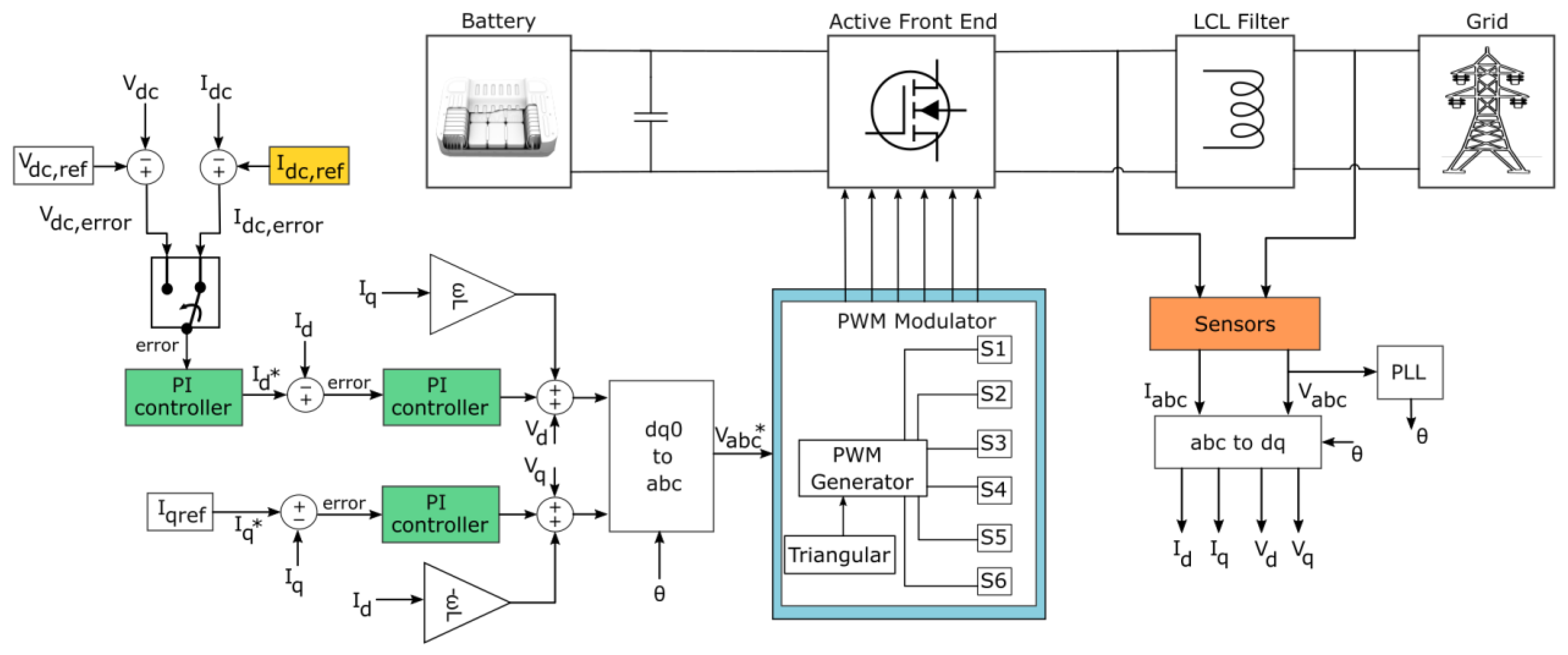
The low-level controller plays an important role in the reliability performance of the off-board charger since it assigns a pulse width modulation (PWM) signal to the six switches of the AFE converter inside the off-board charger to attain a fast-dynamic response and stability during charging and discharging. As shown in Figure 3, a constant current constant voltage (CC-CV) controller is employed to regulate the DC current and the DC voltage using AC grid side current control in a dq-reference frame. However, since the smart charging scheduling algorithm can only provide a reference for the DC current, only the CC control is applied.
For the inner I d and I q current control loops and the outer CC-CV control loop, three proportional integral (PI) controllers are employed. To design the PI controllers a state-space linear model of the converter, as described in [22], is used. After a closed-loop control design analysis, including the sensors and PWM delays, they are tuned according to the margins i.e., gain margin (gM) and phase margin (PM), and frequencies i.e., gain crossover frequency (ωcg) and phase crossover frequency (ωcp). Table 2 specifies the final control parameters of the controllers.
Based on the controlled PWM signals from the low-level controller, the AFE converter allows controlling the transferred power between the grid and the battery. In this paper, SiC-based power switches are modelled considering the following physical phenomena: (a) switching behavior, (b) conduction behavior and (c) thermal behavior. Through the controlled PWM signals originating from the low-level controller, the switches inside the AFE are turned on and off and accordingly power losses arise.

2.4. Electro-Thermal Modelling

Based on electrical responses of the MOSFETs and the anti-parallel body diodes (i.e., drain-to-source voltage V ds and drain-to-source current I ds ), a high-fidelity electro-thermal model of the AFE converter is used to accurately estimate the power losses and the corresponding junction temperature of the SiC power MOSFETs and the body diodes. The electro-thermal model combines a universal loss model of a semiconductor power switch and a thermal model. The loss model estimates the instantaneous power dissipation at a specific junction temperature, while the thermal model determines the temperature gradients inside the converter based on these power losses. For the loss modelling, multi-dimensional lookup tables, as detailed in [23], are used to simplify the relation between voltage, current and temperature. The required data for the lookup tables can be extracted from the datasheet of the considered SiC power module.
The total power dissipated in a MOSFET, or a body diode comprises conduction losses P cond and the switching losses P sw [W], as expressed in Equation (7):
P loss , ( M / d )   = P cond , ( M / d )   +   P sw , ( M / d )  
The instantaneous conduction losses in the MOSFET arise when it is turned on and can be represented as expressed in Equation (8):
P cond , inst , M   = V ds ( I ds , T j ) · I ds
where V ds denotes the voltage drop over the MOSFET [V] and I ds the conducted drain current [A]. V ds is a function of the drain current and the junction temperature T j and can be derived from the datasheet of the MOSFET.
The anti-parallel body diode also has instantaneous conduction losses, which can be calculated using Equation (9):
P cond , inst , d   =   V f ( I f , T j ) · I f
where V f is the forward saturation voltage of the diode [V], which is a function of the forward current I f [A] and the junction temperature T j [K].
The average conduction losses across the MOSFET and the body diode during a switching cycle t sw can be found by integrating the instantaneous conduction losses over this cycle, as expressed in Equation (10):
P cond , ( M , d ) = 1 t sw 0 t sw P cond , inst ( M , d ) dt
The switching losses in the MOSFET arise during the turn-on and turn-off transition. They can be calculated as the sum of the energy losses that occur during a switching transition, as expressed in Equation (11):
P sw , M   =   f sw · ( E M , on ( I ds , V ds , T j ) + E M , off ( I ds , V ds , T si ) )
where f sw is the switching frequency [kHz] and E M , on and E M , off are the energy losses during the on-state and off-state [mJ]. Both switching energy losses are a function of the conducted current, the drain voltage, and the junction temperature.
The switching losses in the body diode mainly occur at turn-off because of its reverse recovery characteristics and can be represented as expressed in Equation (12). Usually, the switching losses over the body diode are negligible, which means that they are often ignored in power loss calculations.
P sw , d = f sw · E d , off ( I f , V f , T j )
where E d , off denotes the turn-off switching energy of the body diode [mJ].
The junction temperature T j of the MOSFET and the body diode can be estimated from the power losses by Equations (13)–(16):
T j = Δ T jc   +   Δ T ch   +   Δ T ha   +   T a
Δ T jc = Z th ( jc ) , ( M / d ) · P loss , ( M / d )
Δ T ch = Z th ( ch ) · n ( P loss , M   +   P loss , d )
Δ T ha = Z th ( ha ) · n ( P loss , M   +   P loss , d )
where Δ T jh is the drop from the junction to the case temperature [K], Δ T ch is the drop from the case to the heatsink temperature [K] and Δ T ha is the drop from the heatsink to the ambient temperature T a [K]. Z th ( jc ) , Z th ( ch ) and Z th ( ha ) are the thermal impedances of the PEC between the junction, the case and the heatsink, respectively [K/W].
Three multi-layer Foster thermal networks are used to represent the heat transfer through the entire PEC. Each layer i of these thermal networks is composed of different thermal resistances R th and thermal capacitances C th whose values are extracted from the datasheet. The thermal impedances can then be calculated from Equation (17).
Z th   = i R th · ( 1 e t R th · C th )
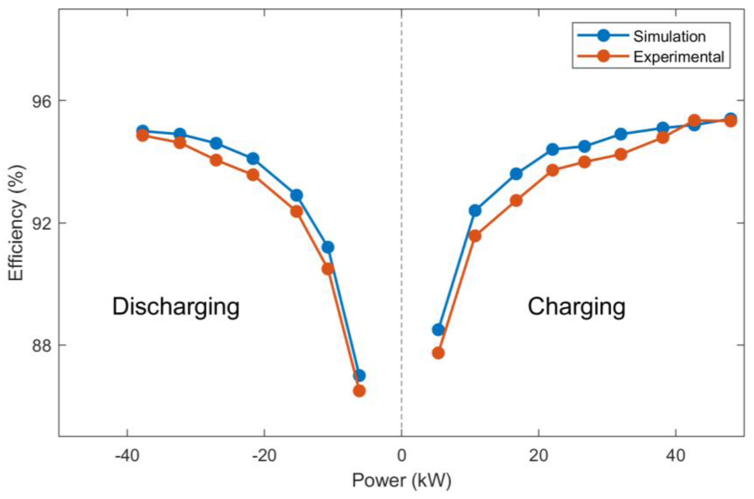
The verification of the analytical electro-thermal model of the AFE converter was performed using the prototype of the charging system, described in [24]. This prototype does not only include the converter, but also the LCL filter. The efficiency was determined by measuring the input and output power in a range from 0 to 50 kW in charging mode and from 0 to −40 kW in discharging mode. With the electro-thermal model, the efficiency η was calculated as expressed in Equation (18).
η = P DC P DC +   P loss , M + P loss , d + P loss , LCL  
with P DC the DC output power of the converter and P loss , LCL the power losses that occur in the passive components of the LCL filter, as detailed in ref. [22].
The resulting curves, depicted in Figure 4, show an accuracy of 98% between the experimental measurements on the prototype and the efficiency estimation of the electro-thermal model. This shows the effectiveness of the electro-thermal model and justifies why it can be used for the junction temperature estimation.

2.5. Lifetime Estimation Framework

Variations in the junction temperature of the MOSFET and the anti-parallel body diode result in thermal stress on these components, which in the end can lead to fatigue failure. To predict the lifetime of the charger, all the thermal cycles need to be extracted from the thermal stress profile. Therefore, a modified rainflow cycle counting algorithm is used, according to [25], which counts the number of cycles N and determines the mean junction temperature T jm , the amplitude of the temperature swing Δ T j and the pulse duration of the MOSFETs t on . To account for the very fast swings that occur in MOSFETs due to high switching frequencies, the algorithm has been modified.
The outcomes of the rainflow cycle counting algorithm are then applied to a “Leistungs Elektronik Systemtechnik und Informations Technologie” (LESIT) parametric SKiM 63 lifetime model to calculate the number of cycles to failure N f of the MOSFET and the body diode as expressed in Equation (19) [26]:
N f =   A · ( Δ T j ) α · ( a r ) β 1 Δ T j + β 0 · [ C + ( t on ) γ C + 1 ] · e ( E a k b   ×   T jm ) · f d
Here, A = 3.4368 × 10¹⁴ denotes the technology factor, C = 1.434, α = −4.983, β 0 = −1.942, β 1 = −9.012 × 10⁻³ and γ = −1.208 are model parameters, a r = 0.31 is the bond wire aspect ratio, f d = 0.6204 is the body diode impact factor, k b = 8.6173 × 10⁻⁵ is the Boltzmann constant [eV/K] and E a = 0.066 is the acteation energy [eV].
The accumulated damage caused by each thermal cycle throughout the lifetimes of the MOSFET and the body diode can be found by using Miner’s linear damage rule, as given in Equation (20).
D = k N k N fk
where D is the accumulated damage, N k is the number of cycles for a constant thermal stress level k determined by to the rainflow cycle counting algorithm and N fk the number of cycles to failure at that specific stress level determined by the lifetime model. When D reaches 1, it is considered that the component reached its end-of-life. The accumulated damage can afterwards be converted into a specific value for the component lifetime.
In practice, a BEB charging system will be subject to many different charging profiles, and accordingly to numerous thermal cycles, during its entire lifetime. Furthermore, due to minor imperfections in the packaging process, the datasheet parameters used in Equation (18) can also differ from what is mentioned by the manufacturer. To consider these uncertainties in the reliability analysis of the charger, slight random variations to the output parameters of the rainflow cycle counting algorithm and the datasheet parameters are introduced by means of a Monte Carlo analysis. A dataset of 10,000 variations of each parameter is generated where all values are normally distributed around the initial value with a standard deviation of 10%.
Next, the two-parameter Weibull probability density function, as expressed in Equation (21), is fitted on the resulting datasets of the MOSFET and the body diode to obtain the shape parameter β and the scale parameter η .
f ( t ) = β η ( t η ) β 1 e ( t η ) β for   t 0
The shape parameter is particularly useful for reliability assessments and indicates if the failure rate is decreasing, constant or increasing. If β < 1 , a component fails due to factory defects. If β = 1 , failures occur independent of time during the useful lifetime of the component. If β > 1 , a component fails because it wears out. The failure rate then typically increases with time. The scale parameter represents the time when 63.2% of the components will have failed.
Once the shape parameter and scale parameter are known, the reliability in function of time of the MOSFET ( R M ) and body diode ( R d ) can be determined from Equation (22).
R ( M , d ) ( t ) = e ( t η ) β
The reliability of the entire charging system can be computed based on the failure association of the different individual components. For this study, only the six SiC MOSFETs and six anti-parallel body diodes are considered. Because the system lacks redundancy, the charger immediately breaks down if a failure occurs in any of these components. Accordingly, simply multiplying the reliability of the components will return the overall system-level reliability, as expressed in Equation (23).
R charger = R M 6 · R d 6
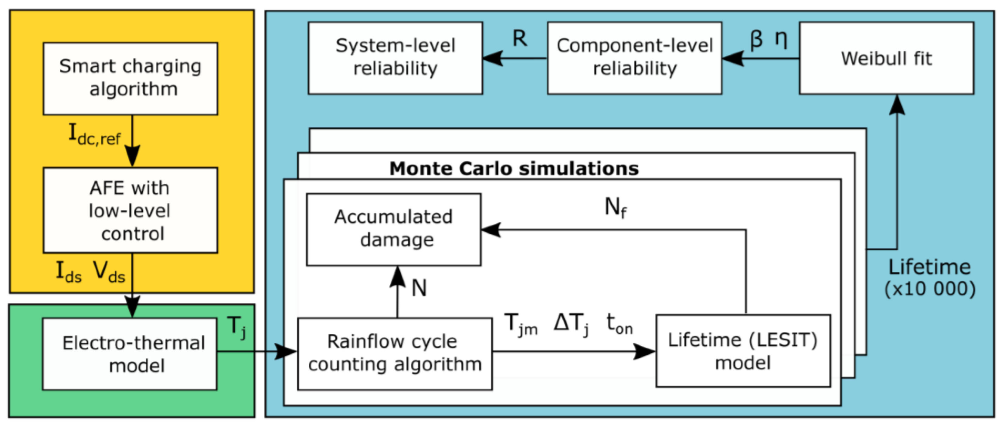
An overview of the complete stepwise methodology to estimate the system-level reliability is presented in Figure 5.

3. Results & Discussions

To perform a meaningful reliability analysis, the considered charging system is subjected to four different charging profiles used to charge a standard 12 m BEB. It is assumed for all charging profiles that the BEB arrives at the depot with an almost empty battery pack and that it needs 252 kWh to get fully charged (which equals to an electric driving range of 180 km, assuming an average energy expenditure of 1.4 kWh/km [13]). Different electricity tariff and grid limitation schemes are considered to obtain diverse charging profiles.
The four charging profiles include one conventional uncoordinated charging profile (‘baseline’), where no load variation occurs during charging and three smart charging profiles generated by the charging scheduling algorithm as described in the previous section. From these three smart charging profiles, one profile (‘smart 1’) only involves charging operation with small load variations, a second charging profile (‘smart 2’) includes a long period of discharging operation, and the last charging profile (‘smart 3’) involves more frequent load variations in charging mode and a short discharging period. The considered charging profiles are depicted in Figure 6.
The charging current profiles are used as an input for the low-level controller. The resulting electrical responses of the MOSFET and the anti-parallel body diode are in their turn used as an input for the electro-thermal model to estimate the junction temperature during operation. An ambient temperature of 45 °C is considered as reliability assessments are most interesting at worst-case scenarios.
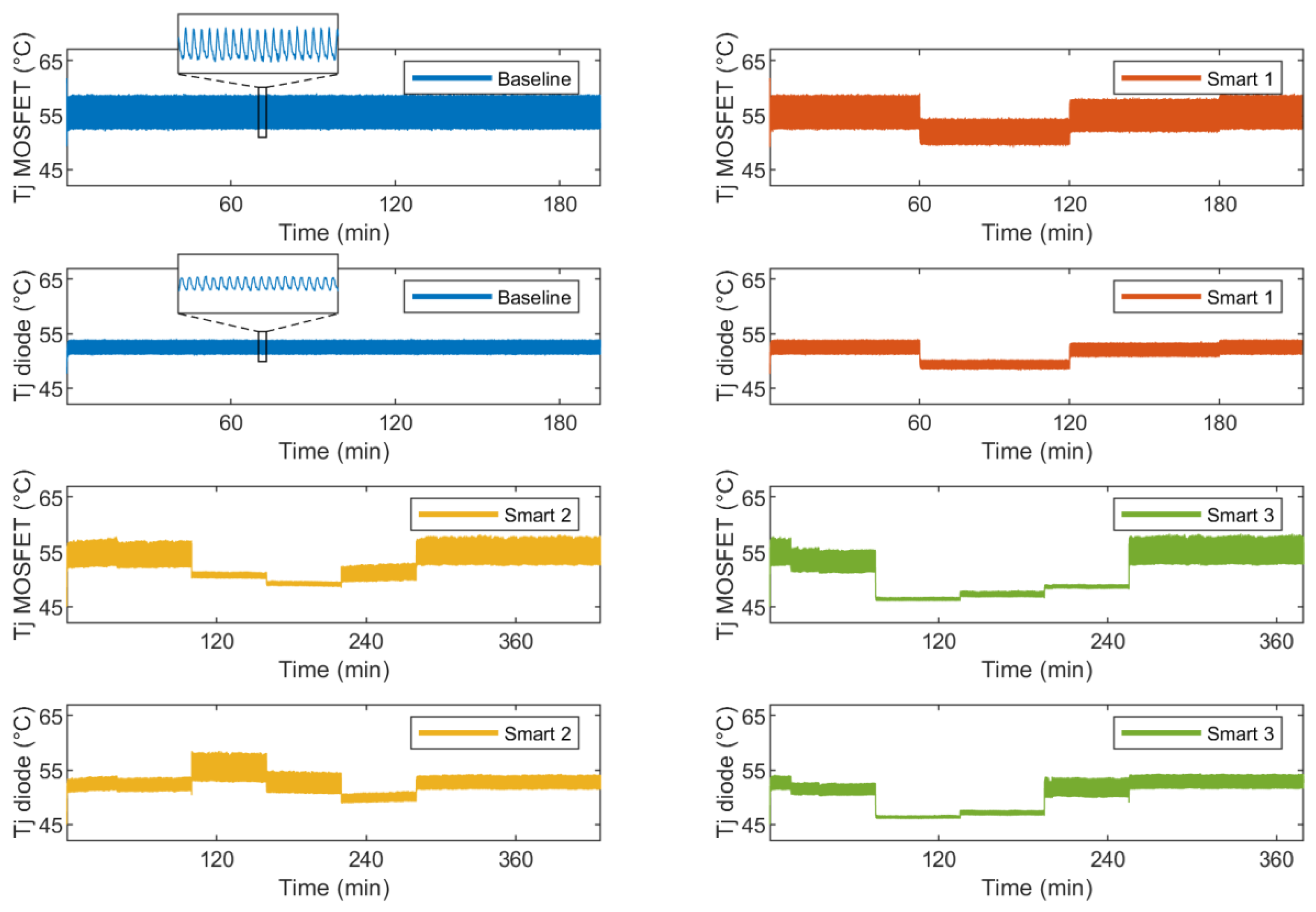
The junction temperature profiles of the MOSFET and the body diode corresponding to the applied charging current profiles are shown in Figure 7. First, it can be noticed that the temperature profiles show a somewhat similar behavior to the charging current profiles in Figure 6.
The junction temperature decreases when the absolute value of the charging current decreases and vice versa. Furthermore, it can be observed from the zoomed in portion of baseline profile that the temperature does not remain constant, but that it swings around a mean value. To a certain degree, the amplitude of the swing is proportional to the mean value of the junction temperature. In the charging phase, the junction temperature of the MOSFETs is higher than the one of the body diodes, due to the higher switching losses of the MOSFET. However, in discharging mode, this is not the case. Here, the body diode has a higher junction temperature because the current flow is reversed, and the diode is conducting.
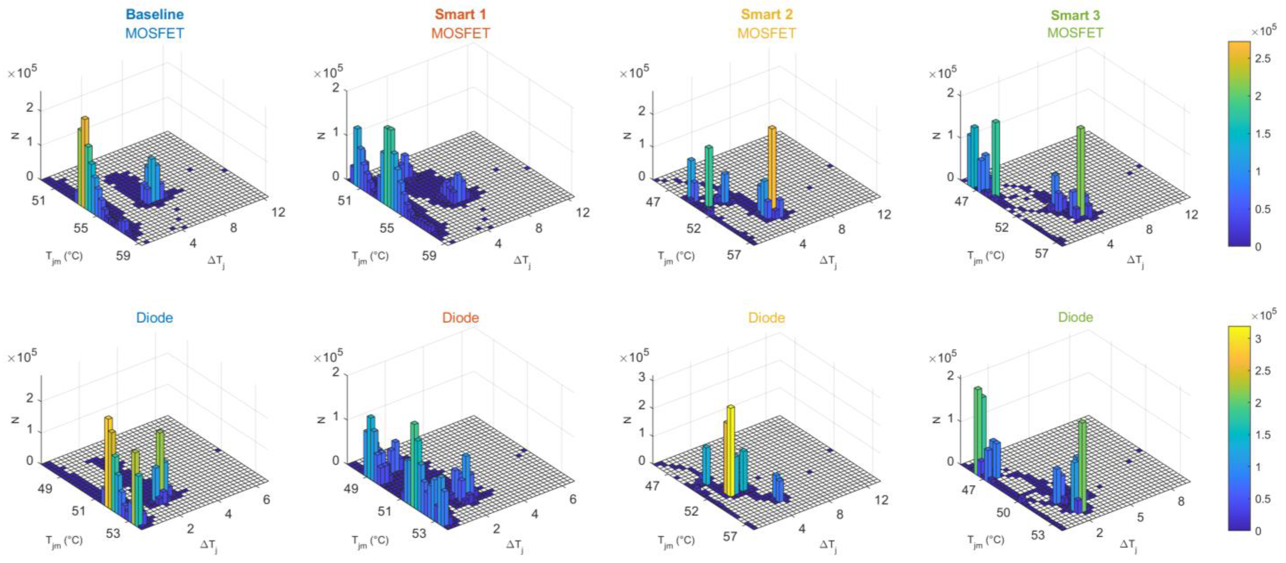
The purpose of the rainflow cycle counting algorithm is to extract the number of cycles or half-cycles from load or stress measurement data. In this case, the load inputs to the algorithm are the junction temperature profiles of the MOSFETs and the body diodes. Figure 8 shows the results of the rainflow cycle counting algorithm as a two-dimensional histogram of the number of cycles (N) as a function of the mean junction temperature ( T jm ) and the swing in the junction temperatures ( Δ T j ). It illustrates how many switching cycles are counted under different mean temperature values and also how many cycles are counted for different amplitudes of temperature swings. These two values are very important because they are the leading factors of the degradation of power switching devices as a result of temperature fatigue. Switching devices that experience continuously higher mean temperatures are more likely to fail than switches that experience a lower mean temperature. Similarly, switching devices that experience large temperature swings are more likely to fail than switches that experience small temperature swings. Therefore, it is important to determine how likely (determined by the number of cycles) a switch will experience a certain temperature or temperature swing for a specific scenario.
From Figure 8, it can not only be seen that MOSFETs are more likely to experience higher mean temperatures than body diodes, but also that they experience greater temperature swings. For the four considered scenarios, the maximum temperature swing of the body diodes is around 2 °C, while that of the MOSFET is around 4 °C. Furthermore, for three of the four scenarios, the mean temperatures of the MOSFETs are approximately 4 °C higher than the mean temperature of the body diodes. Thus, it can be expected that the MOSFETs will fail more rapidly than the body diodes over their operating lifetime.
Regarding the considered scenarios, it can be observed that for the ‘baseline’/uncoordinated charging profile and the ‘smart 1’ charging profile, the thermal cycles for both the MOSFET and the body diode are packed around the highest peak. This indicates that high thermal stress is imposed on the components. The ‘baseline’ charging profile experiences the highest number of thermal cycles (approximately 260,000 cycles at a mean junction temperature of 54 °C for the MOSFET and 280,000 cycles at a mean temperature of 52 °C for the body diode). As a result, the ‘baseline’ charging profile will lead to a faster degradation of the MOSFET and the body diode. For the ‘smart 2’ and the ‘smart 3’ charging profiles, the thermal cycles are more dispersed, which is typically more favorable in terms of lifetime. Still, both profiles experience a high number of cycles with a large temperature swing.
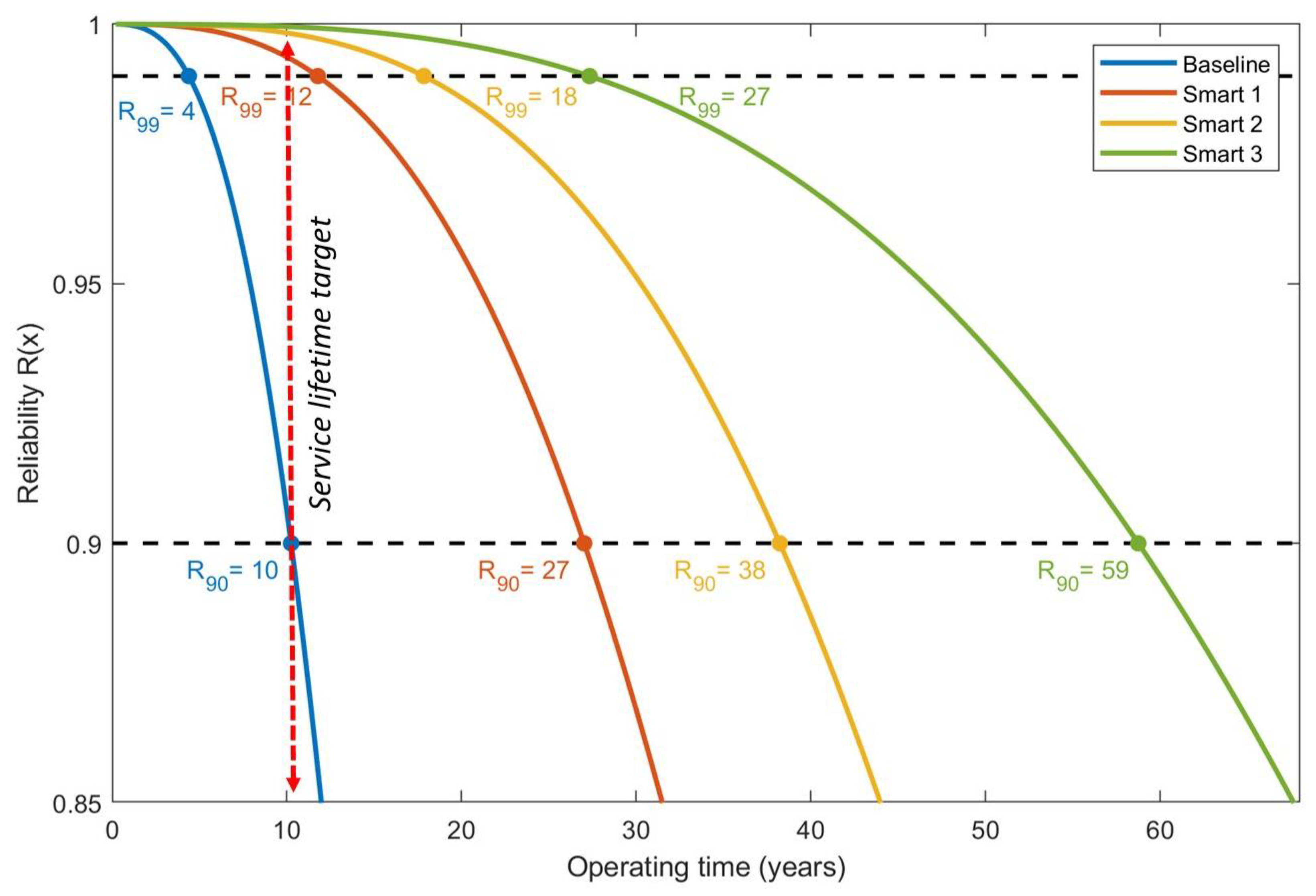
In Figure 9, the overall system reliability of the charger is shown as a function of the operating time in years. As the aim of this paper is to assess the impact of smart and V2X charging strategies on the lifetime of a high-power depot charging system for BEBs, it is assumed that the charging system will daily be subjected to the same charging current profile during its entire operating time. However, to provide a more pragmatic lifetime assessment for BEB charging infrastructure, a deviation in the mission profile parameters is also considered using Monte Carlo simulations, as mentioned in the previous section.
According to [3,27] the point of interest for the lifetime estimation is the 90% reliability percentile ( R 90 ) that is equal to 10% failures of the charging systems after the corresponding operating years. However, in automotive applications, such a higher ~10% probability of failures is not considered as the target point rather focuses on probabilities in parts per million (ppm) range, i.e., 1% failure ( R 99 ).
From Figure 9, it can be seen that only the ‘baseline’/uncoordinated charging profile fails to fulfill the expected lifetime requirement of a 10-year service lifetime in the ppm range (i.e., 99% reliability percentile). This value corresponds to what is generally expected by the automotive equipment manufacturers (OEMs) as service lifetime in the ppm range. On the contrary, for the ‘smart 1’, ’smart 2’, ‘smart 3’ charging profiles, the 99% reliability percentile is reached after 12 years, 18 years and 27 years, respectively.
Besides, for the 90% reliability percentile, all the charging profiles successfully fulfill the OEM’s lifetime requirement. The predicted 90% reliability percentile is exactly 10 years for the ‘baseline’/uncoordinated charging profile. This corresponds with the results of [10], where it was found that the lifetime of the AC/DC converter in an 80 kW fast EV charging system is 12 years, considering an 85% reliability percentile.
For the ‘smart 1’, ’smart 2’, ‘smart 3’ charging profiles, the 90% reliability percentile is reached after 27 years, 38 years and 59 years, respectively. This clearly shows that the applied smart charging strategy can significantly improve the lifetime of a high-power charging system for BEBs. Moreover, it can be stated that bidirectional charging is even more beneficial for such a charging system, as the ‘smart 2’ charging profile increases the reliability of the system compared to the ‘smart 1’ charging profile. Thus, during V2X, the charging system faces less thermo-mechanical stress. The ‘smart 3’ charging profile clearly provides the highest reliability to the system. This is because the charging profile has a prolonged period where the charging current is far off the maximum possible current, which reduces the repetitive temperature swings.
It must be pointed out that in reality, the lifetime of the considered charging system will be lower than the predicted values in Figure 9, as there are other failure types and failure prone components involved (e.g., DC-link capacitor, LCL filter elements, micro-controller, etc.), which have not been considered in the reliability assessment. Furthermore, parameters of a Si-based power device (SKiM 63) were utilized in the LESIT lifetime model since data for SiC power devices are not readily available from the manufacturers. To retrieve such data, accelerated lifetime testing of SiC power devices is required, which is currently still a critical research topic [28,29]. However, the aim of this paper was not to estimate the exact lifetime, but rather to examine how different charging strategies compare to each other in terms of reliability and to explore the possible benefits of utilizing smart and bidirectional charging.

4. Conclusions

With the increasing demand for BEBs in cities, smart charging with V2X functionalities will become indispensable in large depots to reduce the charging cost and avoid grid overloading. Still, one of the major concerns for the PTOs is the lifetime of the charging infrastructure. Therefore, in this paper, a stepwise reliability estimation framework has been developed to assess the impact of smart and bidirectional (V2X) charging on the lifetime of SiC-based high-power off-board chargers for BEBs in depots.
Three different smart charging current profiles, all having their own specific characteristics, were used for the reliability analysis and were compared with the conventional uncoordinated charging strategy. The results have shown that the smart and bidirectional charging profiles are favorable, as the uncoordinated charging profile fails to fulfill the lifetime requirement in the ppm range. On top of that, all the smart charging current profiles significantly improved the lifetime. Smart charging, where only small load variations are applied, can improve the lifetime by at least a factor of three, while more frequent load variations can make the charging system up to six times more reliable. Bidirectional charging has proven to be even more beneficial for the lifetime of the charging system than unidirectional charging with small load variations, as it further improves the lifetime by a factor of one and a half. These results are extremely valuable for PTOs planning to install bidirectional depot charging systems and to implement smart charging scheduling strategies to reduce their charging costs and their peak load.
In future research, accelerated lifetime testing of the SiC-based power switches through power cycling will be considered to investigate additional failure modes and obtain a more accurate lifetime estimation of the charging system. Furthermore, an online cloud-based health monitoring framework using predictive maintenance and inventory management strategies could be implemented to ensure the reliability and the serviceability for a failure-free operation of a depot charging system and a reduction of the maintenance costs for PTOs.

Author Contributions

Conceptualization, B.V. and S.C.; methodology, B.V., H.R., M.M.H. and S.C.; investigation, B.V. and S.C.; software, B.V., H.R., S.C. and M.M.H.; validation, B.V., M.M.H. and S.C.; writing—original draft preparation, B.V., H.R. and M.M.H.; writing—review and editing, S.C., T.G., M.E.B. and O.H.; visualization, B.V.; supervision, O.H.; project administration, S.C.; funding acquisition, O.H. All authors have read and agreed to the published version of the manuscript.

Funding

This work was conducted in the framework of the BELLA project. This project has received funding from VLAIO (ex. IWT) and Flux50 funding schemes in Belgium under project ID: HBC.2021.0800.

Data Availability Statement

The data presented in this study are available on request from the corresponding author. The data are not publicly available due to confidentiality.

Acknowledgments

The authors acknowledge the BELLA project (project ID: HBC.2021.0800) consortium for the support to this research. The authors also acknowledge Flanders Make for the support to our research group.

Conflicts of Interest

The authors declare no conflict of interest.

References

  1. Transport and Environment (T&E). Addressing the Heavy-Duty Climate Problem. Brussels, Belgium, September 2022. Available online: https://www.transportenvironment.org/discover/addressing-the-heavy-duty-climate-problem/ (accessed on 23 November 2022).
  2. Gandoman, F.H.; Ahmadi, A.; Bossche, P.V.D.; Van Mierlo, J.; Omar, N.; Nezhad, A.E.; Mavalizadeh, H.; Mayet, C. Status and future perspectives of reliability assessment for electric vehicles. Reliab. Eng. Syst. Saf. 2018, 183, 1–16. [Google Scholar] [CrossRef]
  3. Blaabjerg, F.; Wang, H.; Vernica, I.; Liu, B.; Davari, P. Reliability of Power Electronic Systems for EV/HEV Applications. Proc. IEEE 2020, 109, 1060–1076. [Google Scholar] [CrossRef]
  4. Hanif, A.; Yu, Y.; DeVoto, D.; Khan, F.H. A Comprehensive Review Toward the State-of-the-Art in Failure and Lifetime Predictions of Power Electronic Devices. IEEE Trans. Power Electron. 2018, 34, 4729–4746. [Google Scholar] [CrossRef]
  5. Li, S.; Lu, S.; Mi, C.C. Revolution of Electric Vehicle Charging Technologies Accelerated by Wide Bandgap Devices. Proc. IEEE 2021, 109, 985–1003. [Google Scholar] [CrossRef]
  6. Ding, X.; Du, M.; Zhou, T.; Guo, H.; Zhang, C. Comprehensive comparison between silicon carbide MOSFETs and silicon IGBTs based traction systems for electric vehicles. Appl. Energy 2017, 194, 626–634. [Google Scholar] [CrossRef]
  7. Yu, S.; Wang, J.; Zhang, X.; Liu, Y.; Jiang, N.; Wang, W. The Potential Impact of Using Traction Inverters with SiC MOSFETs for Electric Buses. IEEE Access 2021, 9, 51561–51572. [Google Scholar] [CrossRef]
  8. Chakraborty, S.; Hasan, M.M.; Paul, M.; Tran, D.-D.; Geury, T.; Davari, P.; Blaabjerg, F.; El Baghdadi, M.; Hegazy, O. Real-Life Mission Profile-Oriented Lifetime Estimation of a SiC Interleaved Bidirectional HV DC/DC Converter for Electric Vehicle Drivetrains. IEEE J. Emerg. Sel. Top. Power Electron. 2021, 10, 5142–5167. [Google Scholar] [CrossRef]
  9. Barbagallo, C.; Rizzo, S.A.; Scelba, G.; Scarcella, G.; Cacciato, M. On the Lifetime Estimation of SiC Power MOSFETs for Motor Drive Applications. Electronics 2021, 10, 324. [Google Scholar] [CrossRef]
  10. Karunarathna, J.; Madawala, U.; Baguley, C.; Blaabjerg, F.; Sandelic, M. Reliability Analysis of Fast Electric Vehicle Charging Systems. In Proceedings of the 2021 IEEE 12th Energy Conversion Congress & Exposition—Asia (ECCE-Asia), Singapore, 24–27 May 2021; pp. 1607–1612. [Google Scholar] [CrossRef]
  11. Manzolli, J.A.; Trovão, J.P.; Antunes, C.H. A review of electric bus vehicles research topics—Methods and trends. Renew. Sustain. Energy Rev. 2022, 159, 112211. [Google Scholar] [CrossRef]
  12. Pearre, N.S.; Ribberink, H. Review of research on V2X technologies, strategies, and operations. Renew. Sustain. Energy Rev. 2019, 105, 61–70. [Google Scholar] [CrossRef]
  13. Jahic, A.; Eskander, M.; Schulz, D. Charging Schedule for Load Peak Minimization on Large-Scale Electric Bus Depots. Appl. Sci. 2019, 9, 1748. [Google Scholar] [CrossRef] [Green Version]
  14. Elliott, M.; Kittner, N. Operational grid and environmental impacts for a V2G-enabled electric school bus fleet using DC fast chargers. Sustain. Prod. Consum. 2022, 30, 316–330. [Google Scholar] [CrossRef]
  15. Fan, H.; Wang, D.; Yu, Z.; Du, L. Bi-Level Optimal Scheduling of Electric Bus Fleets in Regional Integrated Electricity-Gas-Heat Energy Systems. IEEE Trans. Transp. Electrif. 2022. [Google Scholar] [CrossRef]
  16. Verbrugge, B.; Rauf, A.M.; Rasool, H.; Abdel-Monem, M.; Geury, T.; El Baghdadi, M.; Hegazy, O. Real-Time Charging Scheduling and Optimization of Electric Buses in a Depot. Energies 2022, 15, 5023. [Google Scholar] [CrossRef]
  17. Rafique, S.; Nizami, M.; Irshad, U.; Hossain, M.; Mukhopadhyay, S. A two-stage multi-objective stochastic optimization strategy to minimize cost for electric bus depot operators. J. Clean. Prod. 2021, 332, 129856. [Google Scholar] [CrossRef]
  18. Manzolli, J.A.; Trovão, J.P.F.; Antunes, C.H. Electric bus coordinated charging strategy considering V2G and battery degradation. Energy 2022, 254, 124252. [Google Scholar] [CrossRef]
  19. Houbbadi, A.; Trigui, R.; Pelissier, S.; Redondo-Iglesias, E.; Bouton, T. Optimal Scheduling to Manage an Electric Bus Fleet Overnight Charging. Energies 2019, 12, 2727. [Google Scholar] [CrossRef] [Green Version]
  20. Yang, S.; Bryant, A.; Mawby, P.; Xiang, D.; Ran, L.; Tavner, P. An Industry-Based Survey of Reliability in Power Electronic Converters. IEEE Trans. Ind. Appl. 2011, 47, 1441–1451. [Google Scholar] [CrossRef]
  21. Verbrugge, B.; Hasan, M.M.; Rasool, H.; Geury, T.; El Baghdadi, M.; Hegazy, O. Smart Integration of Electric Buses in Cities: A Technological Review. Sustainability 2021, 13, 12189. [Google Scholar] [CrossRef]
  22. Rasool, H.; Verbrugge, B.; Zhaksylyk, A.; Tran, T.M.; El Baghdadi, M.; Geury, T.; Hegazy, O. Design Optimization and Electro-Thermal Modeling of an Off-Board Charging System for Electric Bus Applications. IEEE Access 2021, 9, 84501–84519. [Google Scholar] [CrossRef]
  23. Chakraborty, S.; Mazuela, M.; Tran, D.-D.; Corea-Araujo, J.A.; Lan, Y.; Loiti, A.A.; Garmier, P.; Aizpuru, I.; Hegazy, O. Scalable Modeling Approach and Robust Hardware-in-the-Loop Testing of an Optimized Interleaved Bidirectional HV DC/DC Converter for Electric Vehicle Drivetrains. IEEE Access 2020, 8, 115515–115536. [Google Scholar] [CrossRef]
  24. Rasool, H.; Verbrugge, B.; Jaman, S.; Abramushkina, E.; Geury, T.; El Baghdadi, M.; Hegazy, O. Design and Real-Time Implementation of a Control System for SiC Off-Board Chargers of Battery Electric Buses. Energies 2022, 15, 1434. [Google Scholar] [CrossRef]
  25. Samavatian, V.; Iman-Eini, H.; Avenas, Y. An efficient online time-temperature-dependent creep-fatigue rainflow counting algorithm. Int. J. Fatigue 2018, 116, 284–292. [Google Scholar] [CrossRef]
  26. Wintrich, A.; Nicolai, U.; Tursky, W.; Reimann, T. Application Manual Power Semiconductors; SEMIKRON International GmbH: Nuremberg, Germany, 2011. [Google Scholar]
  27. Karimi, S.; Zadeh, M.; Suul, J.A. A Multilayer Framework for Reliability Assessment of Shore-to-Ship Fast Charging System Design. IEEE Trans. Transp. Electrif. 2021, 8, 3028–3040. [Google Scholar] [CrossRef]
  28. Baba, S.; Gieraltowski, A.; Jasinski, M.T.; Blaabjerg, F.; Bahman, A.S.; Zelechowski, M. Active Power Cycling Test Bench for SiC Power MOSFETs—Principles, Design, and Implementation. IEEE Trans. Power Electron. 2020, 36, 2661–2675. [Google Scholar] [CrossRef]
  29. Pu, S.; Yang, F.; Vankayalapati, B.T.; Akin, B. Aging Mechanisms and Accelerated Lifetime Tests for SiC MOSFETs: An Overview. IEEE J. Emerg. Sel. Top. Power Electron. 2021, 10, 1232–1254. [Google Scholar] [CrossRef]
Figure 1. Overview of the charging system and control architecture.
Energies 16 00153 g001
Figure 2. (a) Topology of the off-board charger and (b) detailed pinout of semiconductor under test (SiC half-bridge power module) with (1) middle point of half-bridge: source of upper MOSFET/drain of lower MOSFET; (2) source of half-bridge; (3) drain of half-bridge; (4) gate of upper MOSFET; (5) source of upper MOSFET; (6) gate of lower MOSFET; (7) source of lower MOSFET.
Energies 16 00153 g002
Figure 3. Low-level controller of the off-board charger.
Energies 16 00153 g003
Figure 4. Efficiency comparison between the simulated electro-thermal model and the experimental measurements on the charging system.
Energies 16 00153 g004
Figure 5. Stepwise reliability estimation method for the considered charging system.
Energies 16 00153 g005
Figure 6. Charging current profiles used for the reliability analysis.
Energies 16 00153 g006
Figure 7. Junction temperature profiles of the MOSFET and the body diode for the applied charging current profiles.
Energies 16 00153 g007
Figure 8. Results of the rainflow cycle counting algorithm for the considered charging current profiles.
Energies 16 00153 g008
Figure 9. Weibull reliability of the charging system for the considered charging current profiles.
Energies 16 00153 g009
Table 1. Specifications of the considered off-board charger.
ParameterValue
Maximum power (kW)100
Power factor0.99
Switching frequency (kHz)40
AC voltage (V)400
DC voltage range (V)600–800
Power electronic moduleSiC half bridge module (CAS300M17BM2)
Table 2. Control parameters of the PI controllers.
ControllerControl ParametersgM
(dB)
PM (deg)ωcp (rad/s)ωcg (rad/s)
Id/Iq
Current Control
Kp = 1.8, Ki = 18,41143.965.11.51 × 1047.86 × 105
Vdc/Idc
Voltage/Current control
Kp = 0.25, Ki = 1843.986.22812.45 × 104
Disclaimer/Publisher’s Note: The statements, opinions and data contained in all publications are solely those of the individual author(s) and contributor(s) and not of MDPI and/or the editor(s). MDPI and/or the editor(s) disclaim responsibility for any injury to people or property resulting from any ideas, methods, instructions or products referred to in the content.