Article

Charging Mobile Devices in Indoor Environments

1
Departamento de Eletrónica Telecomunicações e Informática, Instituto de Telecomunicações, Universidade de Aveiro, 3810-193 Aveiro, Portugal
2
Huawei Technologies Sweden AB, 16494 Kista, Sweden
*
Author to whom correspondence should be addressed.
Energies 2022, 15(9), 3450; https://doi.org/10.3390/en15093450
Submission received: 19 March 2022 / Revised: 27 April 2022 / Accepted: 28 April 2022 / Published: 9 May 2022
(This article belongs to the Special Issue Next Generation Wireless Charging System for Mobile Devices)

Abstract

:
Wireless power transfer promises to revolutionize the way in which we use and power mobile devices. However, low transfer efficiencies prevent this technology from seeing wide scale real-world adoption. The aim of this work is to use quasioptics to develop a system composed of a dielectric lens fed by a phased array to reduce spillover losses, increasing the beam efficiency, while working on the antenna system’s Fresnel zone. The DC-RF electronics, digital beamforming and beam-steering by an FPGA, and radiating 4 × 4 microstrip patch phased array have been developed and experimented upon, while the lens has been designed and simulated. This paper details these preliminary results, where the phased array radiation pattern was measured, showing that the beam is being generated and steered as expected, prompting the lens construction for the complete system experimentation.

1. Introduction

Research on wireless power transfer (WPT) has been performed since the experiments of Heinrich Hertz [1] and Nikola Tesla [2,3] in the 19th century. Since then, two main technology areas can be identified: coupling and radiative WPT.
The first of which includes the near-field electromagnetic (EM) effects, such as capacitive and inductive coupling, which are useful for a very limited range. A review of near-field WPT can be found in [4]. These have been developed significantly, having reached the point of commercial implementation, with most household electronics, including mobile phones, having the possibility of being wirelessly charged.
The main limitation of near-field WPT is its limited range, as most applications work only up to a few centimeters. Therefore, the transmitting and receiving devices must be very close together and usually have to be properly aligned, restricting the components’ movement. Important implementations of near-field WPT can be found, nonetheless, such as in biomedical applications [5] or EV charging [6].
On the other hand, radiative WPT consists in using antennas for radiating EM energy that will propagate through space. In order to achieve high-beam efficiency, the radiation should be focused and directed towards a receiving device. This WPT category has also seen intense research, ever since the work of William Brown [1,7]. He proved the viability of these systems by focusing microwave beams into targets, developing highly efficient WPT experiments that still hold records today. Following his work, several nations became interested in radiative WPT, with multiple projects starting all over the world [8,9,10].
Although long range systems have been proposed, radiative WPT has to be further developed before being widely implemented in real-life scenarios. This is mainly due to low overall efficiencies. One of the most problematic areas is the beam efficiency, mainly due to spillover losses and low coupling to radiating elements. To increase it, this work supports itself on the quasioptical (QO) theory [11], which studies EM radiation by comparing it to gaussian beams, taking into account the beam divergence. The authors have experience with this theory as previous work has been developed that used reflectors for focusing beams in WPT systems [12,13].
Regarding the implementation of the quasioptical theory in WPT systems, there have not been system-wide studies relating the gaussian beam with the system paramters. Even in the early days of WPT, William Brown used focusing components for reducing the spillover losses but did not include QO analysis. Nevertheless, this theory has been used for studying components of WPT systems, such as antennas [14,15], beam propagation [16,17] or focusing elements [18,19]. We here propose a system that integrates quasioptics in the system development, for achieving high efficiency.
During recent years, some works have been developed regarding active phased arrays, especially for communication scenarios. For example, ref. [20] presents a 16-element phased-array with 4-bit phase shifters capable of operating from 43–45 GHz resorting to a 0.18- μ m BiCMOS technology from satellite communications. Each of this 16-element arrays is then a sub-array of a 20 × 20 element array to achieve high antenna gain and transmitted power. In [21] the authors present an active phased array using commercial Radio Frequency Integrated Circuits (RFICs) from Anokiwave. The main contribution lies in implementing circularly polarized phased array antennas that use the RFIC beamformers and can achieve an axial ratio bandwidth of 32% under the 3-dB standard limit. Moreover, the system can track a device using an ultrasonic command system that covers up to 30 of the azimuth angle.
On the other hand, some researchers have dedicated their interests to applying this kind of structure in WPT systems. In [22], the authors present a 32-element active integrated phased array capable of providing up to 42 W of output power. The antennas proposed have circular polarization, and a 4-bit digital phase shifter based on a microstrip switch-line is used to control the phase of each element. In [23], it is also presented a 32-element active phased array that delivers a total power of 120 W that aims to power up a rover. To perform the phase shift, a 4-bit digital phase shifter based on FET Switches is used, allowing to cover an azimuth angle from −23 to 23 . In this work, a rectenna on the receiver side collocated at 2.5 m of distance. In this experiment, the energy collected was insufficient to power up the rover.
Additionally, WPT in the Fresnel zone has also been pursued. The work presented in ref. [24] uses planar arrays of rectangular patches for transferring power at a distance of 40 cm. Two 8 × 8 arrays were developed and used for the transmitter while a 4 × 4 array is used as the receiver. The difference between both the transmitting arrays is the phase distribution, achieved through different lengths of the microstrip transmission lines that feed the patches. Therefore, there is no possibility of actively controlling the phase of each element and achieve beamforming or beamsteering. This enabled a maximum efficiency of 33.2% for the transmitting array working on the Fresnel zone.
However, the most remarkable is the one developed by Belo in [25], since it was developed especially for WPT and passive/mobile devices purposes. In this work, an electronic steerable phased array WPT system can select, track, and power up a passive wireless sensor network in an azimuth angle range from −45 to +45 . The authors present a radio-frequency identification (RFID) and active/wake-up techniques that allow having a low complexity battery-less device that can be accurately trackable and communicate back to the transmitter. The system can also operate in three different states, each of which provides different power levels depending on the device’s distance. The algorithm that makes the switch between each state is based on the Received Signal Strength Indicator (RSSI), and according to the received power, it is able to know how far away the device is and adjust the gain and the transmitted power.
This work aims to study a more compact and feasible system for transferring power in an indoor environment. Aiming to charge mobile devices, such as phones, quasioptics is used for increasing the beam efficiency. To achieve this goal, a beam launcher and a dielectric lens for focusing the beam must be developed. The first of which is a 4 × 4 microstrip patch phased-array antenna. By controlling each elements’ current distribution, beamforming [15] and beamsteering [26] can be implemented. This phased-array is fed by a transmitter that follows a heterodyne architecture, allowing independent control of each element, while providing up to a maximum of 2 W per element.
Following the Gaussian beam generation, a dielectric lens will be used to focus it [11]. Dielectric lenses have been thoroughly studied in the literature [27], including by this research group [28]. Previous studies of lenses in QO can be found in [11,18,19].
Finally, on the receiving side, a radio-frequency to DC current (RF-DC) converter will be implemented for outputting the transferred power. The output power is used in a feedback channel, whose resonance frequency varies according to the energy received, helping in the control of the transmitter for optimizing the overall WPT efficiency.
All of these components will be explained in the following sections. Starting from an overview of the system architecture, the basics of the transmitter will be explained as well as of quasioptics. Afterwards, the RF-DC conversion and the feedback channel will be discussed. Experimental results have been obtained for the transmitter and phased-array antenna, while simulation results were achieved for the antenna with the dielectric lens.
This manuscript is divided as follows. Section 2 presents an overview of the proposed system, with the focus on the theoretical background, main principles and design considerations of the crucial components of the system. In Section 3 some preliminary results both measured and simulated are shown and analyzed having in mind future improvements in the system performance. Lastly, in Section 4 some final remarks are drawn.

2. System Architecture

The proposed system is composed of a DC current to radio-frequency (DC-RF) converter and power transmitter that will feed a phased array antenna. The beam created will be focused by a dielectric lens. Afterwards, a receiving antenna will be connected to a RF-DC converter, from which the output DC power will be obtained. A feedback channel will be implemented in order to control the transmitter output for increasing the overall efficiency. An overview of the system is represented in Figure 1.
The methodology of this work follows two main principles. The first is that developments will be done according to the energy flow, meaning that the first stage to be researched is the DC-RF converter and power transmitter, followed by the phased-array antenna. Then, the dielectric lens will be studied and finally the feedback channel. The other principle is that every stage starts by being studied theoretically, before being simulated and implemented in practice.
The project’s current stage of development is such that the transmitter has been studied and already developed in practice, while the dielectric lens has been studied and simulated. The feedback channel as only been studied theoretically. This is what will be presented in this paper.

2.1. Active Phased Array Transmitter

The proposed Active Phased Array Transmitter consists of 16 active and independent channels that will feed a 4 × 4 microstrip patch antenna array operating at 5.8 GHz that should provide at least 25 W to a maximum output power of 32 W of RF power in a CW regime. In Figure 2, is presented the block diagram of the transmitter and also the backscatter/receiving module. The backscatter is going to be used for feedback purposes to improve the system efficiency. Moreover, in Figure 3, is depicted a photograph of the complete system assembled with several components, such as DC power supplies, control signals, power distribution, and fans for thermal compensation.
This system considered a LO frequency fixed at 5.1 GHz and an IF frequency of 0.7 GHz that is up-converted by a mixer to the operating frequency of 5.8 GHz. This choice is justified since a phased array must have complete flexibility to control each element’s amplitude and phase difference. There are several ways to achieve this kind of operation, reported in the literature, such as using varactors [29], time delay [30] or based on vector modulators (IQ modulators) [31]. Due to its operation simplicity, an IQ modulator is used on every element to allow the control of phase shift and/or amplitude. Each IQ modulator receives and modulates the 0.7 GHz IF signal that was previously divided into 16 equal signals, as well as the LO signal.
To implement and perform beamforming architectures, following the antenna array theory [26], the phase difference required at each element of the antenna to point the beam to a certain direction ( θ p , φ p ), for a planar and uniform distribution is given by:
ψ ( n , m ) = k d n s i n ( θ p ) c o s ( φ p ) + k d n s i n ( θ p ) s i n ( φ p ) , n = 1 , , N , m = 1 , , M
where k is the wavenumber, d is the inter-element spacing, and n and m are the indexes of the (n, m) element. Then to set the appropriate phase and amplitude for all 16 elements, a dense digital-to-analog converter (DAC) was selected. The chip is a complete single-supply, with 40-channel and 14-bit resolution that is controlled with the FPGA using SPI connection. With this, each DAC is controlled by a 14-bit word that will produce a signal with a certian amplitude and phase shift ( ψ ), the IQ values sent to each channel in decimal representation are given by:
I ( n , m ) = r o u n d 2 14 2 + a n . m 2 14 2 c o s ( ψ )
I ( n , m ) = r o u n d 2 14 2 + a n . m 2 14 2 s i n ( ψ )
where a n , m is referring to the amplitude control of the (n, m) element.
Since each RF path (each channel) will present different responses in terms of phase and gain/attenuation that feeds each antenna element, a calibration procedure is needed to compensate for those differences. For that, a full calibration is needed to create a LUT that will be used to calculate the correct value to produce a radiation pattern in a specific direction in both azimuth and elevation planes.

2.2. Quasioptics for Enhancing the Beam Efficiency

One of the main losses in WPT systems are related to the beam propagation, mostly due to spillover losses and unoptimized coupling to the radiating components, resulting in low beam efficiency. Quasioptics (QO) can be used to deal with these issues since it helps understand and control microwave beams and their propagation by adapting the results of the theory of optics, to contexts characterized by high beam divergence.
Due to it, the EM radiation can no longer be effectively represented by thin rays. Instead, the fundamental block of QO is the comparison of microwave radiation to gaussian beams, whose basics will now be explained. Gaussian beams are mathematical entities with known behavior: the first assumption is the beam propagation axis, where, if assumed to be in the z ^ direction, z 0 is the point where the power is most concentrated and the divergence less evident. At this point the radiation is a planar wave with no phase shift between the electric field distribution. Gaussian beams are described with various modes of propagation, but the most useful for WPT is the fundamental mode, in which the power is mostly concentrated on the main lobe. Therefore the beam is axially symmetric, depending only on the distance from the axis of propagation (radius), r, and the position along the axis, z:
E ( r , z ) = 2 π ϖ 2 exp r 2 ϖ 2 i k z i π r 2 λ R + i ϕ 0 .
The quantities in (4) are the beam radius, ϖ , the wave front’s radius of curvature, R, the phase shift, ϕ 0 , and the wavelength, λ . Of all of these, the beam radius is especially important for WPT, as it is defined as the radial distance where the power density falls to 1 / e of the value on the propagation axis, with e being the Euler’s number. The minimum value of the beam radius is called the beam waist, ϖ 0 , and is located in z 0 , being a characteristic of the beam.
Gaussian beams can be transformed using the matricial formalism: by representing any QO system through a matrix, M s y s ,
M s y s = 1 d o u t 0 1 · A B C D · 1 d i n 0 1
and the effect the system has on the microwave beam is understood by the relationship between the input and output beam waist, ϖ 0 i n and ϖ 0 o u t , and its distance to the system, d i n and d o u t , respectively:
d o u t = ( A d i n + B ) ( C d i n + D ) + A C z c 2 ( C d i n + D ) 2 + C 2 z c 2
and
ϖ 0 o u t = ϖ 0 i n ( C d i n + D ) 2 + C 2 z c 2 .
Another important parameter, included in (7), is the confocal distance, z c = π ϖ 0 2 / λ . This gives us the distance from z 0 where the beam in which the beam has minimum divergence, remaining relatively collimated.
Finally, the coupling of gaussian beams and radiating antennas is given by a comparison between both their electric field distributions. The resulting coupling efficiency, η G , provides information about how well the antenna radiates and receives the radiation [11,32]:
η G = E A · E G * 2 d x d y | E A | 2 d x d y | E G | 2 d x d y

2.3. Antenna Array and Dielectric Lens

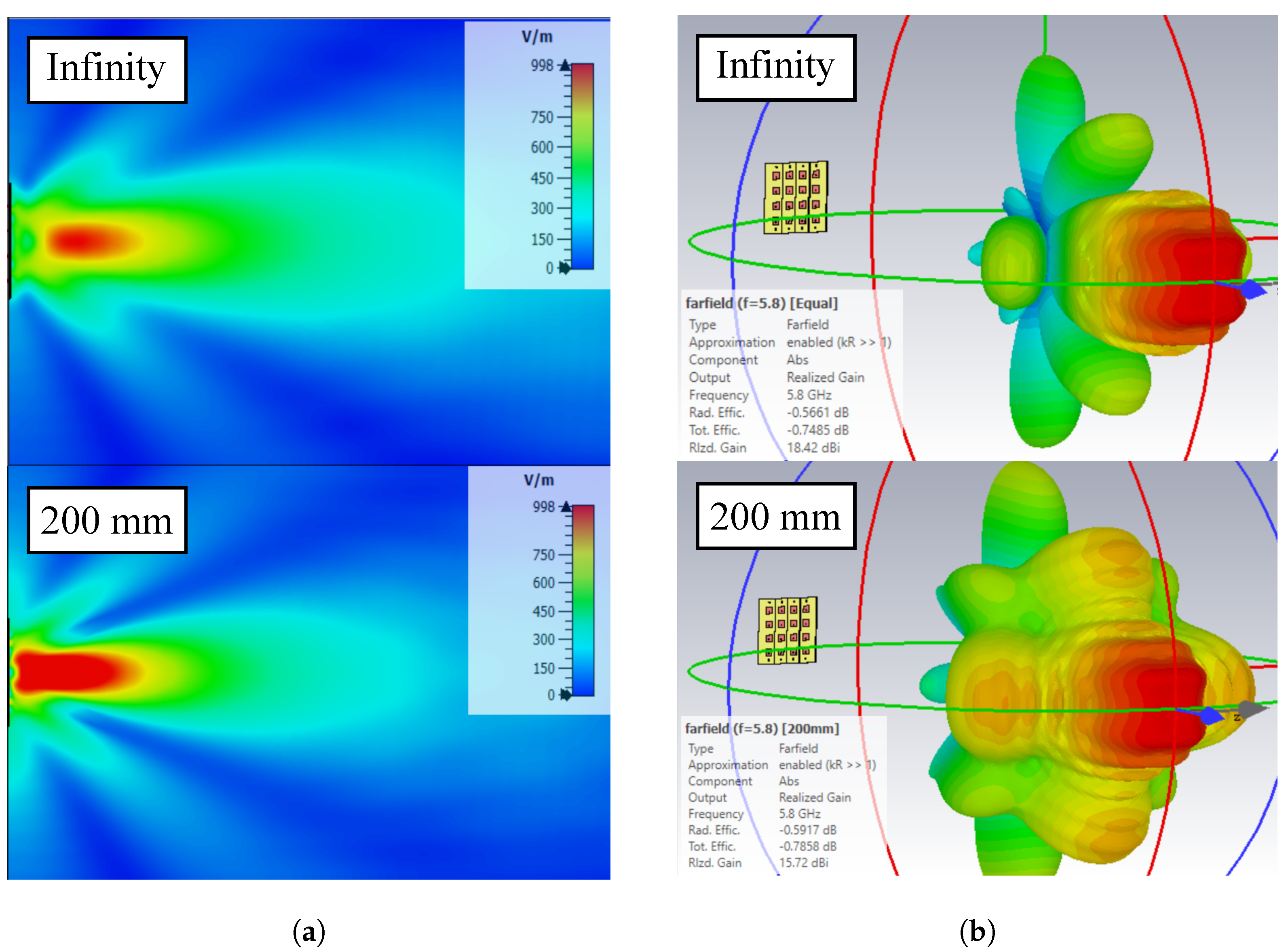
When attempting to transfer power, the beam efficiency must be maximized, which is done here by focusing the energy through a dielectric lens, which means the system works in the antennas’ Fresnel zone. A phased array antenna composed of 4 × 4 microstrip patches was developed to perform beamforming and beamsteering, by controlling the current distribution of each element. These were respectively implemented according to the principles found in [15,26].
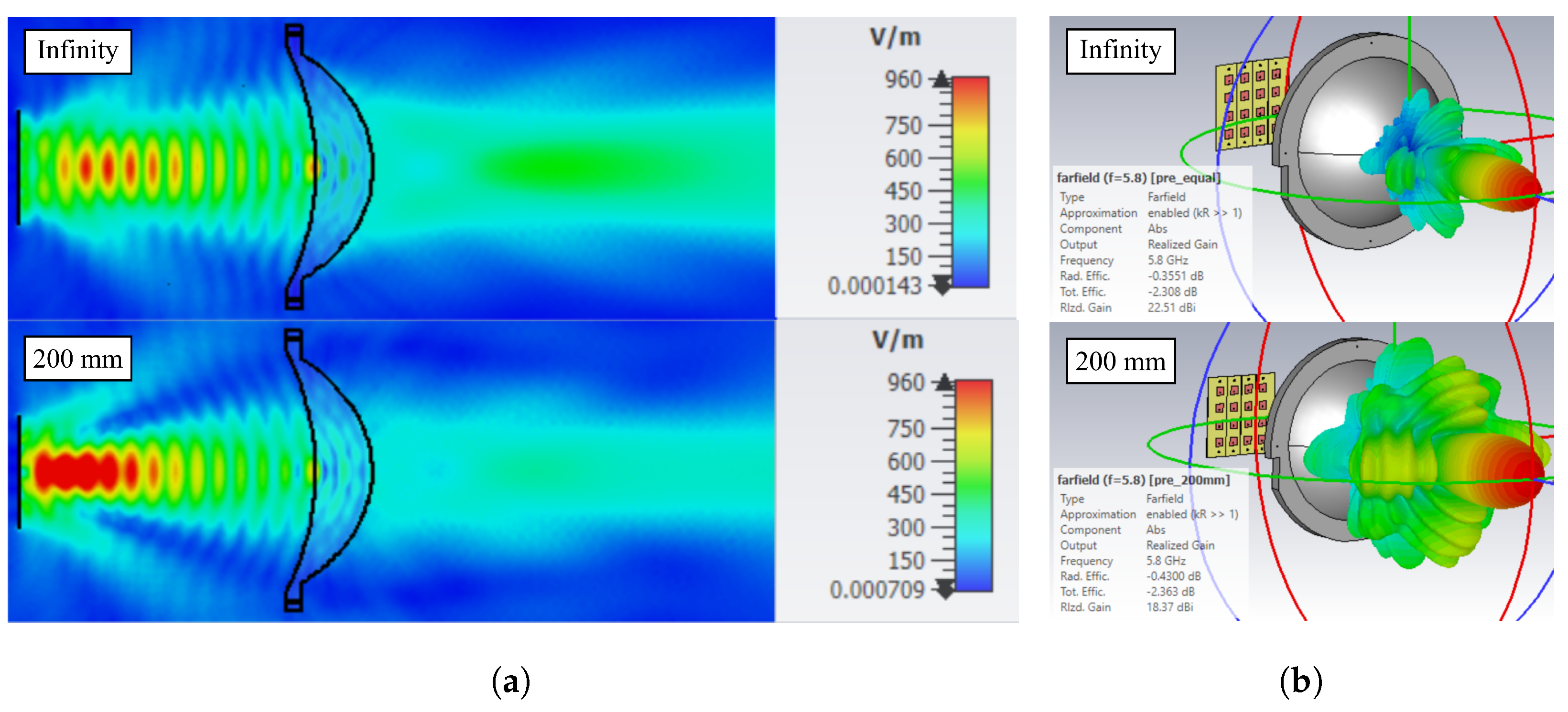
Knowing the expected gaussian beam radiated by the phased array, a dielectric lens was studied for transforming the beam in order to reduce the spillover losses. By keeping the beam radius smaller that the receiving aperture, the receiver collects the majority of the energy, and if it is located at the beam waist, the wave front is planar, enabling the best coupling to planar rectennas. The lens was chosen to have a spherical and elliptical surface, respectively, in order to reduce its reflectivity, and was designed according to [11,33].

2.4. Feedback Channel

In this section, we show the design and theory of the receiving node that should be able to be selected and tracked by the developed transmitter. It is used separate link for the pilot signal, the node will be able to continuously receive the energy that is being transmitted to it, while being able to transmit a signal back to the transmitter with useful information. The block diagram of this node is depicted in Figure 4. The main blocks of the receiving node are a high-power and efficient RF-to-dc converter circuit, a variable frequency oscillator and a load. The remaining of this section is dedicated to provide a detailed description of each of these components.

2.4.1. RF-DC Converter

An RF-DC converter can be divided into three parts, the matching impedance network, the rectifier and the DC filter, as seen in Figure 5a. In the case of this work, the rectifier used was a voltage multiplier.
In order to design the matching impedance network and the DC filter, it is essential to take into account the impedance that they will impose on the rectifier, as it has a significant impact on the diode’s performance. So, to ensure that the blocks are matched to the rectifier, one of the most important steps when designing an RF-DC converter is the source and load-pull simulations. For this, the ADS software was used. The schematic used for this simulation can be found in Figure 5b. To simulate the matching impedance network, it was used the S2P_Eqn block in which the impedance Gamma_source was made varied to find the adequate impedance for the rectifier.
On the other hand, to simulate the DC filter, the chosen block was the S1P_Eqn, in which the Gamma_load variable was varied to simulate the load impedance. With this simulation, it was possible to conclude that for a high input power of 30 dBm, the rectifier requires low impedance from the source’s side, as it is possible to observe in Figure 5c. In the case of the load impedance, the load-pull simulation showed that it was required an impedance of 0.064 j 0.465 .
The chosen filter for the output was a class-R filter (Figure 5d), based on [34]. The substrate used to simulate the microstrip lines is the Rogers RO4003C with a thickness of 0.508 mm, a dielectric constant of 3.38 and a dissipation factor of 0.0027 . The source-pull simulation was re-made with the R-filter implemented instead of a load block.
The final RF-DC converter can be found in Figure 5e. The simulated efficiency and output voltage can be observed in Figure 5f,g with an efficiency of 61% for 30 dBm calculated with Equation (9).
η ( % ) = 100 * P o u t P i n = 100 * V o u t D C 2 R o u t * P i n

2.4.2. Feedback Signal Generation

After the RF-DC conversion, the voltage obtained at the output indicates how much power is generated in the receiver. Then it is necessary through a feedback channel to pass this information to the transmitter so that the direction of the beam can be adjusted for the best efficiency. Therefore, the most important component of this module is a low-power Voltage Controlled Oscillator (VCO) whose oscillation frequency is controlled by a tuning voltage. That voltage corresponds to the output voltage of the RF-DC converter (DC out) depicted in Figure 5g. As this feedback channel can be powered independently, a battery and a voltage regulator are used to provide the supply voltage for the VCO. The frequency of the feedback signal is around 2.4 GHz and depends on the DC output voltage of the RF-DC converter. This frequency varies some MHz so that the Feedback Signal Receiver can identify the frequency through the spectrum analyzer and convert it to the voltage measured in the RF-DC output through a look-up table that contains the correspondences between the oscillation frequency and the VCO tunning voltage. The Feedback Signal Receiver is a Front end of Software-Defined Radio implemented in the FPGA. This FPGA also incorporates a mini spectrum analyzer responsible for analyzing and detecting the transmitted oscillation frequency. Then depending on the corresponding voltage value, it can adjust the direction of the transmitted beam using the scanning algorithm developed. The graphic of Figure 6 shows the VCO characterization in a laboratory environment. The chosen components for the system allow for adjusting the tuning voltage from 0 V to 10 V, thus meeting the minimum and maximum possible voltages for the output of the RF-DC converter. The feedback channel frequency, the same as the Output frequency in the graph, is between 2.10 GHz and 2.59 GHz, so both transmitter and receiver use Microstrip Patch antennas with coaxial feed projected for the center frequency (2.35 GHz) with 500 MHz bandwidth.

3. Preliminary Results and Discussion

This section presents several results, both measured and simulated, obtained at the time of writing, for the different parts of the system. Further analysis will be performed in each of the following subsections.

3.1. RF Boards Validation

With the first characterization setup was intended to characterize each one of the four boards developed, in terms of the amplitude and phase of the output signal. For a setup composed by a VSG that is responsible for generate the LO and IF frequencies (5.1 GHz and 700 MHz respectively), power supply sources that provide the DC bias for the different elements in the boards. Then each output of the board is connected to a VNA that will measure the amplitude and phase of the received signals, as shown in Figure 7.
In Figure 7, the phases of all 16 channels are presented. It is possible that several combinations of I and Q words are possible to cover a frequency range of 360 (from −180 to 180 ). The amplitude of each channel is not presented since for this characterization the amplitude was maintained equal to 1.
With the values obtained is intended to create a LUT in order to be able, in the future, to control in real time the phase of each channel and provide beamforming capabilities to the system.

3.2. Microwave Beam Focusing

The energy focus is created by generating a Gaussian beam with a phased array and later transforming it through a dielectric lens.

3.2.1. Microstrip Patch Phased-Array Antenna

As described previously, the gaussian beam launcher is a phased array that was designed, simulated and optimized for the frequency of operation of 5.8 GHz in CST Studio Suite, before being built. This optimization resulted in a 4 × 4 array, composed of identical square patches. These are fed by a coaxial connector on the ground plane, located slightly below the patches’ center. The optimized antenna in CST is visible in Figure 8a next to the final manufactured array in Figure 8.
Using this antenna, a study was performed for understanding how to generate different gaussian beams, according to the project’s needs. The beamforming was achieved by altering each elements’ current distribution [15]. Firstly, the elements were separated in groups, according to their distance from the antenna’s central point (Figure 8a). This resulted in three groups, described in Table 1, whose results, after applying specific phase differences, are described in Table 2.
The electric field distribution and antenna gains of the most extreme cases, for a focus at infinity and a focus location at 200 mm, are represented in Figure 9.
Following this study, the antenna array was printed in a PCB and the connectors were soldered to each element’s back. This enabled the measurement of each elements’ return loss and coupling to elements in the same line (Figure 8b), as depicted in Figure 10. All the elements present a return loss of under −10 dB for 5.8 GHz, and coupling between elements of the same line is under −20 dB, both being acceptable values.
The array was then connected to the transmitter board described previously and the complete transmitting system was analyzed in an anechoic chamber, with beam steering having been performed.

3.2.2. Transmitter Radiation Pattern

After validating each PCB and hardware in a laboratory environment, the system was taken to the anechoic chamber in order to measure the radiation pattern, using the results obtained in Section 3.1. As shown in Figure 11, the measurement setup was mounted on the anechoic chamber with the goal of measuring the radiation pattern in several azimuth angles (0 , +30 , and −30 ). For that, the transmitter was rotated manually from −45 to 45 with a step of 5 . The results of these measurements are presented in Figure 11b, and it is possible to observe that, although there is no calibration whatsoever, the results obtained are close to what was expected. With the feedback channel and intelligent algorithms to optimize the necessary amplitudes and phases, the beamwidth will be narrower and provide higher gain and efficiency than what was presented here.
As it is, the results are satisfactory, prompting the development of the next system component, the dielectric lens.

3.2.3. Dielectric Lens

Having studied the phased array, its radiation will be focused by a dielectric lens, in order to create a focus of energy. The lens’ design that was chosen has a spherical and elliptical surface, respectively, for reducing its reflection. The design was based on the principles found in [33], where the lens’ thickness and diameter is related to its focal length.
The antenna and lens system was also simulated in CST. This complete transmission system has the electric field distribution and far field represented in Figure 12. The results obtained are summarized in Table 3.
One can conclude that the beam focused by the dielectric lens is more directive, creating a focus of energy after the lens, which is necessary for high efficiency wireless power transfer. However, the analysis of the gaussian beam still needs to be further developed as the beam outputted from the phased array needs to be determined.
However, the presented results are promising, showing that an antenna and lens system achieves high simulation efficiencies and a beam with controlled divergence, after which we expect to be able to significantly reduce the spillover losses. This prompts further development of the system as high efficiency WPT is expected to be achieved.
Having already built the transmitter and phased array antenna, the dielectric lens will now be manufactured and experimented upon, both for validating the results shown here, but also to perform further study and analysis, mainly about the created gaussian beam and its focus of energy.
The main expected issues with using a system with a lens is that the beamsteering may be limited. This is because, at extreme angles, the beam may miss the lens that is a certain distance from the phased array. If that is the case, there may be a tradeoff between the beamsteering capability and the beam focusing, but these issues need to be studied furtherly. Nevertheless, the advantages of using the lens in terms of beam efficiency far surpass its limitation.

4. Conclusions

This work reports a high-power and efficient Wireless Power Transmitter for charging mobile devices. The proposed system is composed of a RF transmitter that powers a 4 × 4 phased array antenna, as well as a dielectric lens for focusing the radiated beam. The transmitter and antenna have been produced and experimented upon, while the lens has been designed and simulated.
The transmitting board is composed of 16 independent channels that can provide up to 2 W and control over the amplitude and phase of each channel, forming a high-power active phased array for wireless power transfer purposes that is capable of beamforming and beamsteering. Then, since most of the energy is typically lost in the beam propagation due to free space losses, an innovative approach based on the quasioptics theory is proposed for enhancing the beam efficiency and, consequently, the overall system efficiency. To do that, a dielectric lens will create a focus of energy in the Fresnel zone, significantly reducing the spillover losses. The lens has been designed and simulated, with its implementation achieving simulation efficiencies higher than 81.5%.
On the receiving side (mobile device), a feedback channel is implemented that allows the transmitter to locate the received node and improve power transfer efficiency. The receiving node is composed of an RF-DC converter that will convert the RF energy into electrical power. This electrical power will supply a low-frequency oscillator will transmit a signal back to the transmitter, whose frequency will depend on the power received by the RF-DC converter. In this way, it is possible to know how far the receiving node is. Finally, positive preliminary results (measured and simulated) are presented regarding several parts of the system, proving its feasibility for indoor-environment mobile devices charging. Furthermore, the eventual implementation of machine learning or artificial intelligence algorithms on the transmitter, for assuring the optimal amplitude and phase current distribution of each element of the array, will allow the development of commercial WPT systems for device charging.

Author Contributions

D.M. has designed all the transmitter hardware, performed the characterization of the transmitter and wrote the paper. R.A.M.P. has developed the quasioptics theory for WPT, has designed and simulated the antenna and dielectric lens and wrote the paper. H.R. has designed the RF-DC converter and wrote the paper. B.M. has been responsible for the digital control and the characterization of the transmitter. A.O. has supervised the entire research with more focus in digital component, the results analysis and discussion and provided the guidance for writing the paper. N.B.C. and D.B. has supervised the entire research in RF component, the used approach, the results analysis and discussion and provided the guidance for writing the paper. All authors have read and agreed to the published version of the manuscript.

Funding

This research received no external funding.

Institutional Review Board Statement

Not applicable.

Informed Consent Statement

Not applicable.

Data Availability Statement

Not applicable.

Acknowledgments

The authors would like to thank to Huawei Sweden for the support and collaboration in this work. On the other hand, Ricardo Pereira would like to thank the Fundação para a Ciência e a Tecnologia (FCT), Portugal for his grant SFRH/BD/145024/2019.

Conflicts of Interest

The authors declare no conflict of interest.

Abbreviations

The following abbreviations are used in this manuscript:
CWContinuous-Wave
DACDigital-to-Analog Converter
DC-RFDirect Current to Radio Frequency
EMElectromagnetic
FPGAField Programmable Gate Array
IFIntermediate Frequency
IQIn-phase and quadrature
LOLocal Oscillator
LUTLookUp Table
PCEPower Conversion Efficiency
PCBPrinted Circuit Board
QOQuasioptical
RFRadio Frequency
RF-DCRadio Frequency to Direct Current
RFICRadio Frequency Integrated Circuit
RFIDRadio-frequency Identification
RSSIReceived Signal Strength Indicator
SPISerial Peripheral Interface
VCOVoltage Controlled Oscillator
VNAVector Network Analyzer
VSGVector Signal Generator
WPTWireless Power Transfer

References

  1. Brown, W.C. The History of Power Transmission by Radio Waves. IEEE Trans. Microw. Theory Tech. 1984, 32, 1230–1242. [Google Scholar] [CrossRef] [Green Version]
  2. Marincic, A.S. Nikola Tesla and the Wireless Transmission of Energy. IEEE Trans. Power Appar. Syst. 1982, 10, 4064–4068. [Google Scholar] [CrossRef]
  3. Lumpkins, W. Nikola Tesla’s Dream Realized: Wireless power energy harvesting. IEEE Consum. Electron. Mag. 2014, 3, 39–42. [Google Scholar] [CrossRef]
  4. Jawad, A.M.; Nordin, R.; Gharghan, S.K.; Jawad, H.M.; Ismail, M. Opportunities and Challenges for Near-Field Wireless Power Transfer: A Review. Energies 2017, 10, 1022. [Google Scholar] [CrossRef]
  5. Kim, H.J.; Hirayama, H.; Kim, S.; Han, K.J.; Zhang, R.; Choi, J.W. Review of Near-Field Wireless Power and Communication for Biomedical Applications. IEEE Access 2017, 5, 21264–21285. [Google Scholar] [CrossRef]
  6. Mohamed, N.; Aymen, F.; Alqarni, M.; Turky, R.A.; Alamri, B.; Ali, Z.M.; Abdel Aleem, S.H. A new wireless charging system for electric vehicles using two receiver coils. Ain Shams Eng. J. 2022, 13, 101569. [Google Scholar] [CrossRef]
  7. Brown, W.C. The history of wireless power transmission. Sol. Energy 1996, 56, 3–21. [Google Scholar] [CrossRef]
  8. Shinohara, N. History of Research and Development of Beam Wireless Power Transfer. In Proceedings of the 2018 IEEE Wireless Power Transfer Conference (WPTC), Montreal, QC, Canada, 3–7 June 2018; pp. 1–4. [Google Scholar] [CrossRef]
  9. Shinohara, N. History and Innovation of Wireless Power Transfer via Microwaves. IEEE J. Microw. 2021, 1, 218–228. [Google Scholar] [CrossRef]
  10. Rodenbeck, C.T.; Jaffe, P.I.; Strassner, B.H., II; Hausgen, P.E.; McSpadden, J.O.; Kazemi, H.; Shinohara, N.; Tierney, B.B.; DePuma, C.B.; Self, A.P. Microwave and Millimeter Wave Power Beaming. IEEE J. Microw. 2021, 1, 229–259. [Google Scholar] [CrossRef]
  11. Goldsmith, P.F. Quasioptical Systems: Gaussian Beam Quasioptical Propagation and Applications; IEEE Press: Piscataway, NJ, USA, 1998. [Google Scholar]
  12. Pereira, R.A.M.; Carvalho, N.B.; da Cunha, J.P. Quasi-optical analysis of a double reflector microwave antenna system. Wirel. Power Transf. 2018, 5, 75–86. [Google Scholar] [CrossRef] [Green Version]
  13. Pereira, R.A.M.; Carvalho, N.B.; Georgiadis, A. Focus Location Measurement of a Quasioptical Double Reflector System. In Proceedings of the 2021 IEEE Wireless Power Transfer Conference (WPTC), San Diego, CA, USA, 1–4 June 2021; pp. 1–4. [Google Scholar] [CrossRef]
  14. Han, M.; Guan, X.; Einat, M.; Fu, W.; Yan, Y. Investigation on a 220 GHz Quasi-Optical Antenna for Wireless Power Transmission. Electronics 2021, 10, 634. [Google Scholar] [CrossRef]
  15. Takano, T.; Uno, T.; Shibata, K.; Saegusa, K. Generation of a beamed wave using a phased array antenna. In Proceedings of the 2016 URSI Asia-Pacific Radio Science Conference (URSI AP-RASC), Seoul, Korea, 21–25 August 2016; pp. 377–379. [Google Scholar] [CrossRef]
  16. Matsumuro, T.; Ishikawa, Y.; Ishikawa, T.; Shinohara, N. Effective beam forming of phased array antenna for efficient microwave power transmission. In Proceedings of the 2014 Asia-Pacific Microwave Conference, Sendai, Japan, 4–7 November 2014; pp. 717–719. [Google Scholar]
  17. Smith, D.R.; Gowda, V.R.; Yurduseven, O.; Larouche, S.; Lipworth, G.; Urzhumov, Y.; Reynolds, M.S. An analysis of beamed wireless power transfer in the Fresnel zone using a dynamic, metasurface aperture. J. Appl. Phys. 2017, 121, 014901. [Google Scholar] [CrossRef]
  18. Kim, W.G.; Moon, N.W.; Singh, M.K.; Kim, H.K.; Kim, Y.H. Characteristic analysis of aspheric quasi-optical lens antenna in millimeter-wave radiometer imaging system. Appl. Opt. 2013, 52, 1122–1131. [Google Scholar] [CrossRef] [PubMed] [Green Version]
  19. Qin, Y.; Guo, Q. Quasi optic lens antenna with corrugated feed horns. In Proceedings of the ICMMT’98. 1998 International Conference on Microwave and Millimeter Wave Technology. Proceedings (Cat. No.98EX106), Beijing, China, 18–20 August 1998; pp. 382–386. [Google Scholar] [CrossRef]
  20. Koh, K.J.; May, J.W.; Rebeiz, G.M. A Millimeter-Wave (40–45 GHz) 16-Element Phased-Array Transmitter in 0.18-μm SiGe BiCMOS Technology. IEEE J. -Solid-State Circuits 2009, 44, 1498–1509. [Google Scholar] [CrossRef]
  21. Chieh, J.C.S.; Yeo, E.; Farkouh, R.; Castro, A.; Kerber, M.; Olsen, R.B.; Merulla, E.J.; Sharma, S.K. Development of Flat Panel Active Phased Array Antennas Using 5G Silicon RFICs at Ku- and Ka-Bands. IEEE Access 2020, 8, 192669–192681. [Google Scholar] [CrossRef]
  22. Kawasaki, S.; Seita, H.; Suda, T.; Takei, K.; Nakajima, K. 32-Element high power active integrated phased array antennas operating at 5.8 GHz. In Proceedings of the 2008 IEEE Antennas and Propagation Society International Symposium, San Diego, CA, USA, 5–11 July 2008; pp. 1–4. [Google Scholar] [CrossRef]
  23. Kawasaki, S. Microwave WPT to a rover using active integrated phased array antennas. In Proceedings of the 5th European Conference on Antennas and Propagation (EUCAP), Rome, Italy, 11–15 April 2011; pp. 3909–3912. [Google Scholar]
  24. Gowda, V.R.; Yurduseven, O.; Lipworth, G.; Zupan, T.; Reynolds, M.S.; Smith, D.R. Wireless Power Transfer in the Radiative Near Field. IEEE Antennas Wirel. Propag. Lett. 2016, 15, 1865–1868. [Google Scholar] [CrossRef]
  25. Belo, D.; Ribeiro, D.C.; Pinho, P.; Borges Carvalho, N. A Selective, Tracking, and Power Adaptive Far-Field Wireless Power Transfer System. IEEE Trans. Microw. Theory Tech. 2019, 67, 3856–3866. [Google Scholar] [CrossRef]
  26. Balanis, C.A. Antenna Theory: Analysis and Design; John Wiley & Sons, Inc.: Hoboken, NJ, USA, 2005. [Google Scholar]
  27. Fernandes, C.A.; Costa, J.R.; Lima, E.B.; Silveirinha, M.G. Review of 20 Years of Research on Microwave and Millimeter-wave Lenses at “Instituto de Telecomunicaço~es”. IEEE Antennas Propag. Mag. 2015, 57, 249–268. [Google Scholar] [CrossRef] [Green Version]
  28. Gonçalves, R.; Carvalho, N.B.; Pinho, P. Wireless energy transfer: Dielectric lens antennas for beam shaping in wireless power-transfer applications. Comptes Rendus Phys. 2017, 18, 78–85. [Google Scholar] [CrossRef]
  29. Zhang, H.; Ren, H.; Tang, H.; Zheng, B.; Katz, B.; Arigong, B.; Zhang, H. A Microstrip line Reflection-Type Phase Shifter for 60 GHz Phased Array. In Proceedings of the 2019 IEEE MTT-S International Microwave Symposium (IMS), Boston, MA, USA, 2–7 June 2019; pp. 826–829. [Google Scholar] [CrossRef]
  30. Masotti, D.; Costanzo, A.; Del Prete, M.; Rizzoli, V. Time-Modulation of Linear Arrays for Real-Time Reconfigurable Wireless Power Transmission. IEEE Trans. Microw. Theory Tech. 2016, 64, 331–342. [Google Scholar] [CrossRef]
  31. Yang, W.; Zhou, J.; Zhou, K.; Yu, Z. A 5.8-GHz Active Transmitting Array Based on Frequency Shiftable Vector Modulator Module. IEEE Antennas Wirel. Propag. Lett. 2016, 15, 1085–1088. [Google Scholar] [CrossRef]
  32. Karandikar, Y. Factorization of Gaussian Coupling Efficiency and algorithm to compute it. In Proceedings of the 2012 6th European Conference on Antennas and Propagation (EUCAP), Prague, Czech Republic, 26–30 March 2012; pp. 868–872. [Google Scholar] [CrossRef]
  33. Lo, Y.T.; Lee, S.W. Antenna Handbook: Volume II Antenna Theory; Van Nostrand Reinhold: New York, NY, USA, 1993. [Google Scholar]
  34. Miwatashi, K.; Shinohara, N. Development of Class-R Rectifier for Microwave Wireless Power Transmission to EV trucks. In Proceedings of the 2021 IEEE Wireless Power Transfer Conference (WPTC), San Diego, CA, USA, 1–4 June 2021; pp. 1–4. [Google Scholar] [CrossRef]
Figure 1. System overview.
Energies 15 03450 g001
Figure 2. Block Diagram of High-Power Wireless Power Transmitter.
Energies 15 03450 g002
Figure 3. Full Transmitter Assembled with the several components.
Energies 15 03450 g003
Figure 4. Feedback Channel Block Diagram.
Energies 15 03450 g004
Figure 5. High Power and Efficient RF-DC Converter Step-by-Step Design. (a) RF-DC converter block diagram. (b) Schematic of the source and load pull simulation used in ADS. (c) Source-pull simulation. (d) Class-R filter Block Diagram. (e) Schematic of the RF-DC converter. (f) Simulated efficiency. (g) Simulated output voltage.
Energies 15 03450 g005
Figure 6. Relation between Vtune and Oscillation Frequency.
Energies 15 03450 g006
Figure 7. Measurement Setup to characterize the boards developed. (a) Validation and characterization setup using a VNA. (b) Phase differences of all 16 channels with different I and Q words.
Energies 15 03450 g007
Figure 8. (a) Design of the phased array antenna in the CST Studio Suite, where the patch separation into groups is visible. (b) Picture of the printed antenna, with the connectors soldered in place. Beamforming was achieved by grouping the elements as described in Table 1 and applying phase differences, which enable the results summarized in Table 2.
Energies 15 03450 g008
Figure 9. Comparison of the phased array antenna’s electric field distribution (a) and far field gain (b), for a focus at infinity and at 200 mm from the antenna. The results are summarized in Table 2.
Energies 15 03450 g009
Figure 10. Experimental results of the phased array designed for wireless power transfer containing the return loss of each element (a) and the coupling between elements of the same row (b).
Energies 15 03450 g010
Figure 11. Transmitter Radiation Pattern for different Azimuth Angles and respective Measurement Setup. (a) Measurement Setup in Anechoic Chamber. (b) Radiation pattern.
Energies 15 03450 g011
Figure 12. Comparison of the phased array antenna and lens’ electric field distribution (a) and far field gain (b), for a focus at infinity and located at 200 mm from the antenna.
Energies 15 03450 g012
Table 1. Phased-array element separation into groups, according to the distance from each patch center to the overall array central point, where w is the patch width and d is the element separation.
GroupDistanceValue [mm]Elements
A d / 2 21.2136, 7, 10, 11
B d 5 / 2 47.4342, 3, 5, 8, 9, 12, 14, 15
C 3 d / 2 63.6391, 4, 13, 16
Table 2. Details of the radiation produced by varying the electric current distribution feeding the phased array.
Beam WaistMax. E field Max. E field GainEfficiency
Location[V/m]Location [mm][%][%]
Infinity998.26192.34318.4284.17
1000 mm1153.8877.58618.3484.16
500 mm1302.1272.22018.0284.08
400 mm1369.5969.53717.7784.01
300 mm1471.0264.17117.2383.97
200 mm1635.1753.43915.7283.45
Table 3. Far-field simulation results of just the phased-array ( T x ) and phased-array and lens radiating system ( T x + Lens).
Beam WaistGain [dBi]Efficiency [%]
Location T x T x + Lens T x T x + Lens
Infinity18.4224.2584.1784.62
1000 mm18.3423.9284.1684.51
500 mm18.0223.3684.0884.09
400 mm17.7722.9984.0183.78
300 mm17.2322.2583.8783.12
200 mm15.7220.3583.4581.52
Publisher’s Note: MDPI stays neutral with regard to jurisdictional claims in published maps and institutional affiliations.

