
Flyback Converter Using a D-Mode GaN HEMT Synchronous Rectifier


Abstract
:1. Introduction
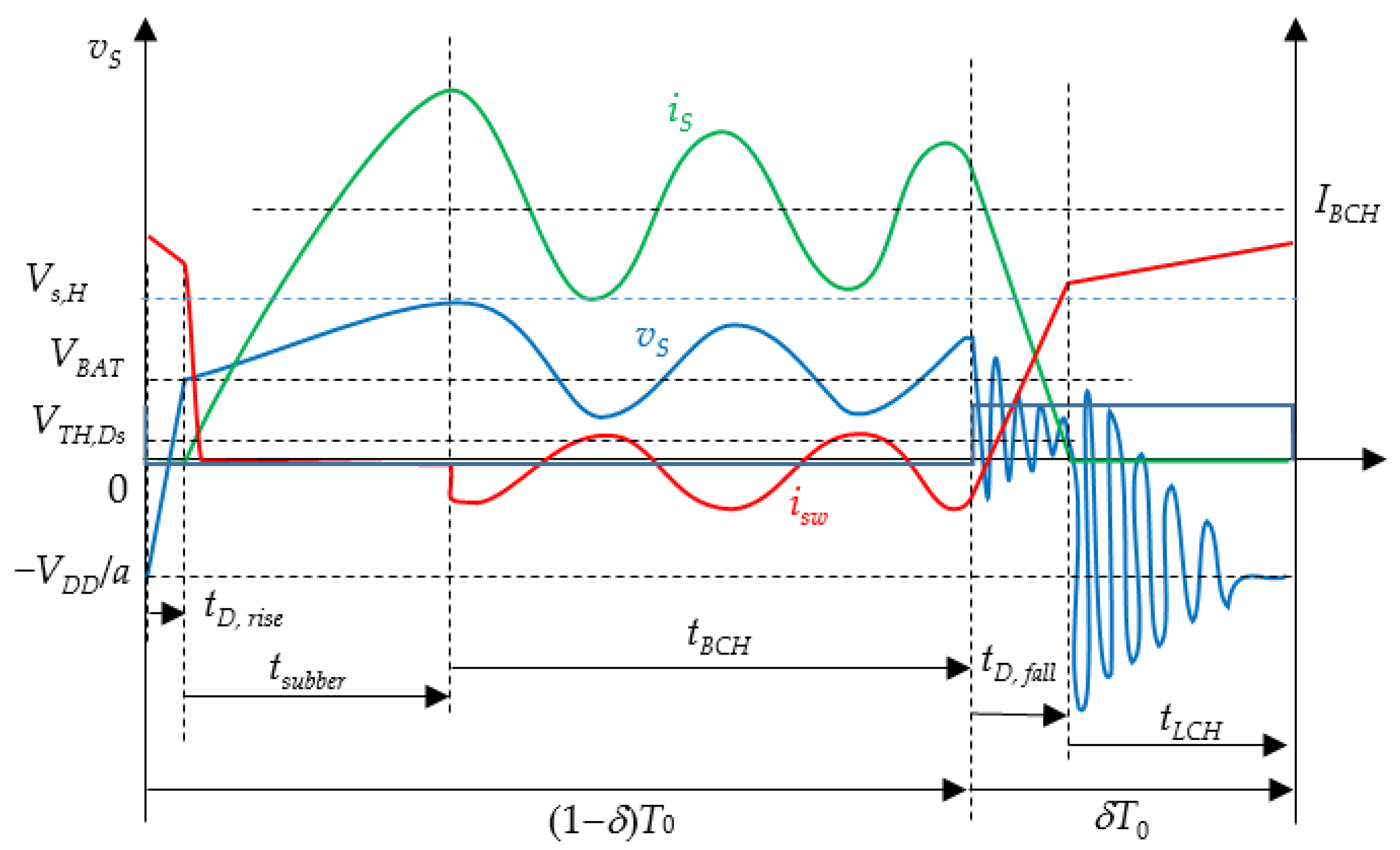
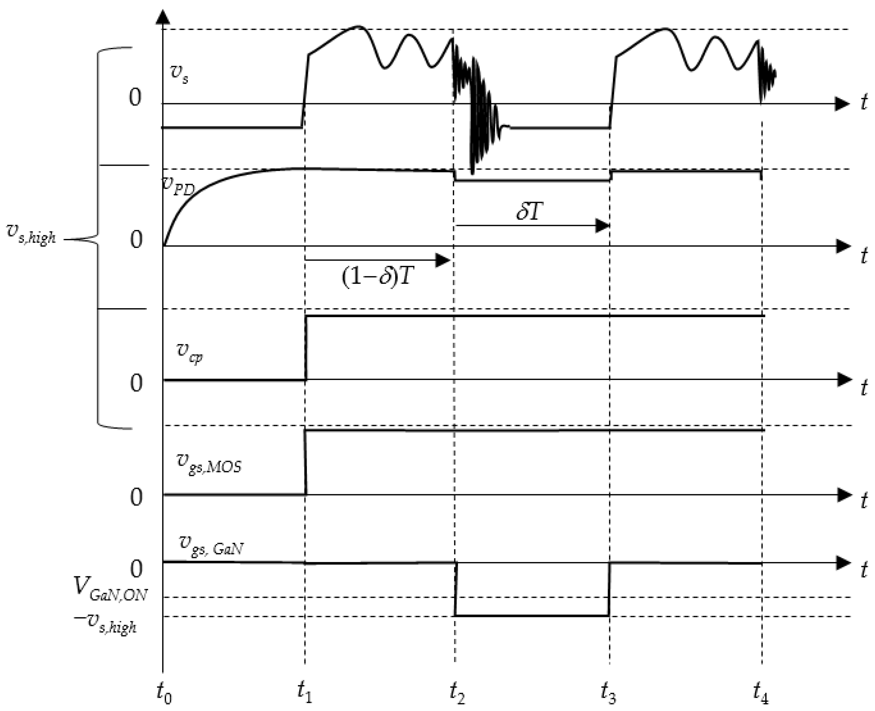
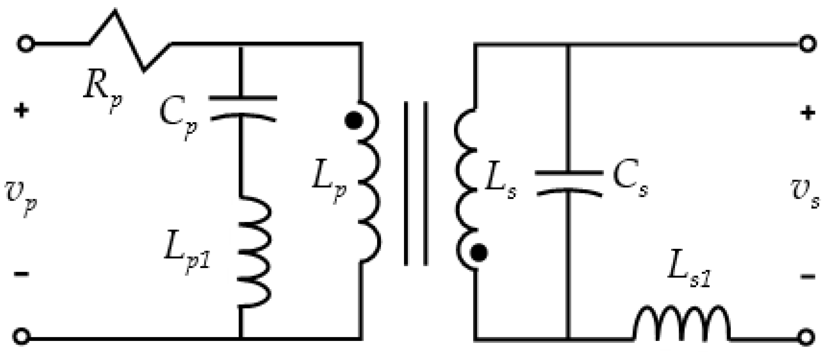
2. Flyback Converter
2.1. Diode Turn-On Period of Time tD,rise
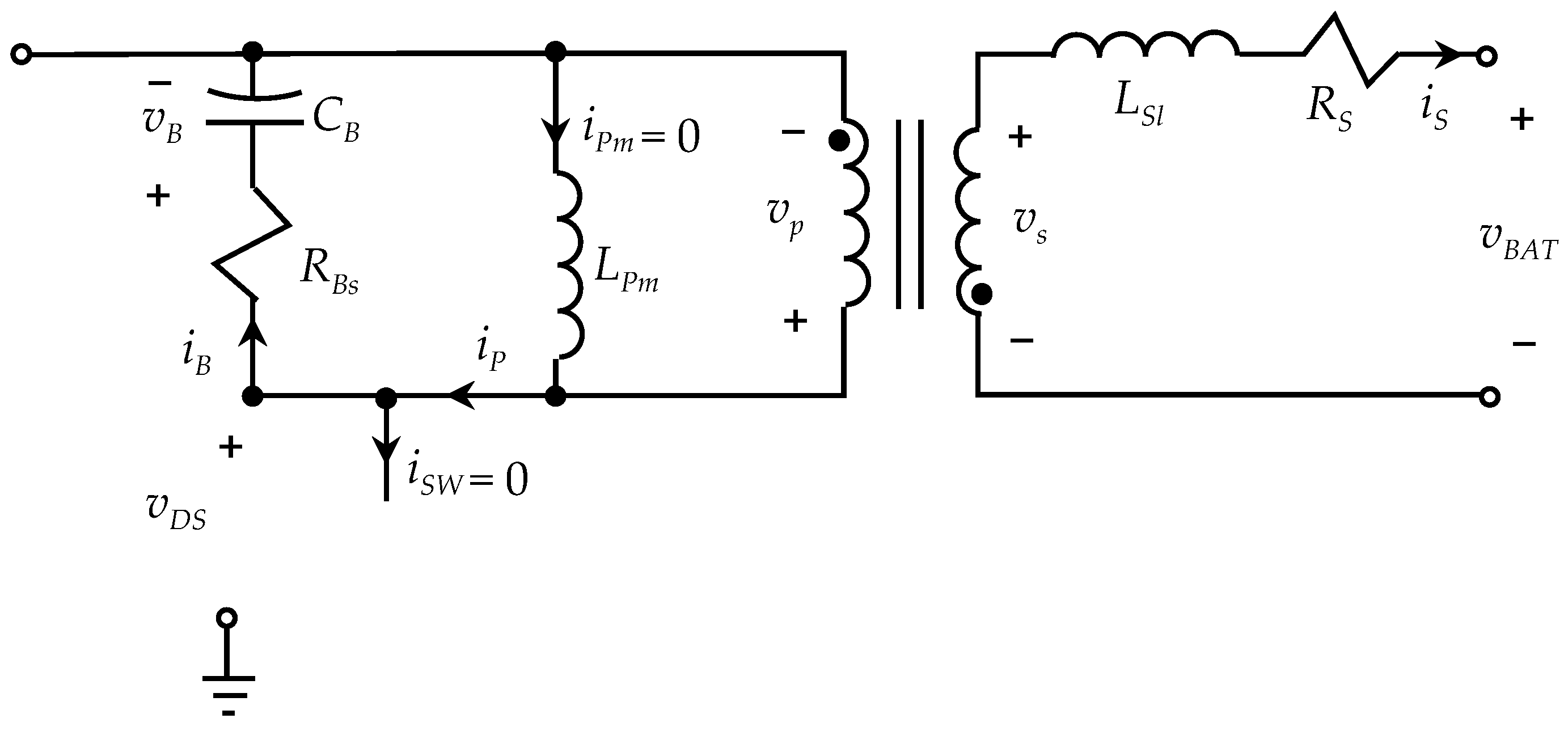
2.2. Snubber Activated Period of Time tsnubber
2.3. Battery Charging Period of Time tBCH
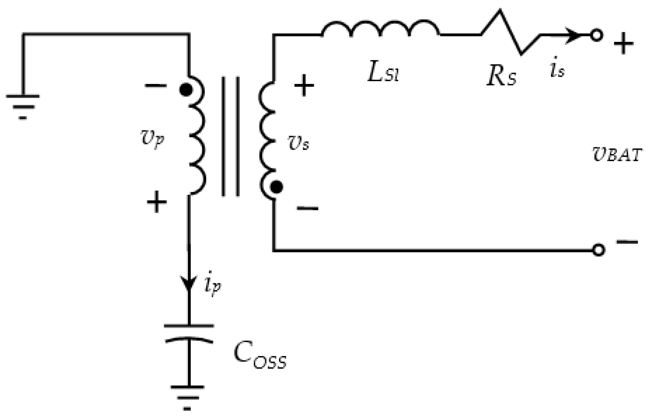
2.4. Diode Turn-Off Period with Time tD,fall
2.5. Inductor Charging Period with Time tLCH
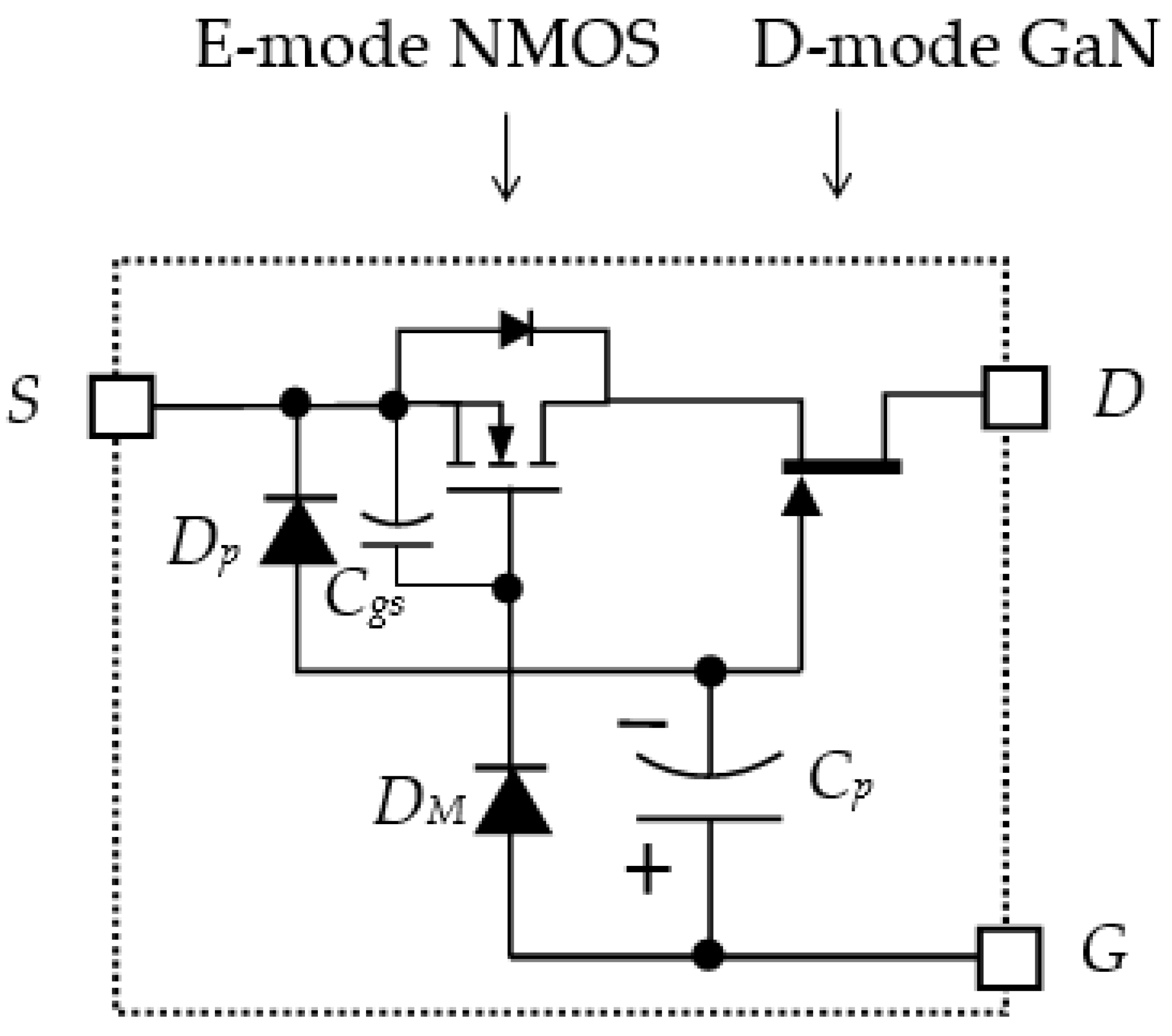
3. D-Mode GaN HEMT Synchronous Rectifier
- It is a normally-on device which is not applicable to block the current flowing to battery during the inductor charging period;
- The power supply system to the GaN HEMT must be self-sustainable on the secondary side when the battery is on low voltage or even empty;
- It shall turn off itself during the reverse bias.
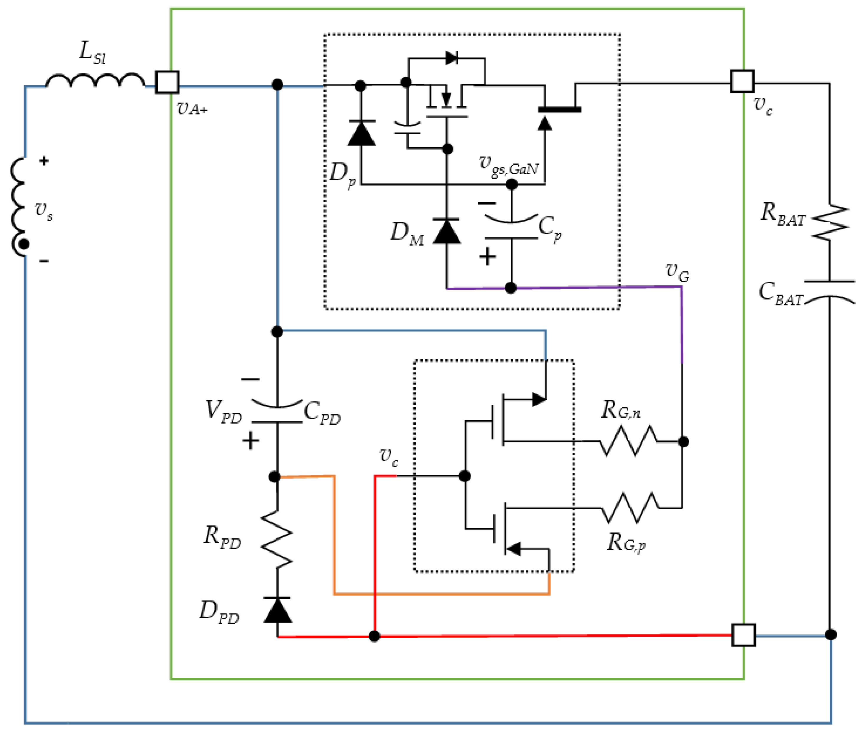
3.1. Cascode GaN HEMT Power Module
3.2. Self-Sustainable Power Supply for Gate Driver
3.3. D-Mode GaN HEMT Synchronous Rectifier
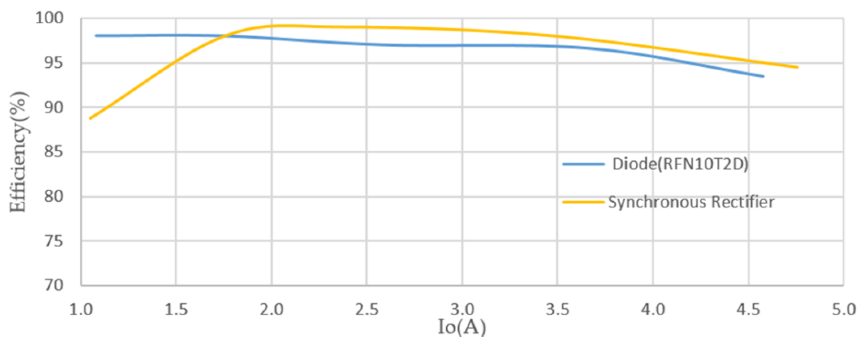
- The threshold voltage for the diode VTH,Ds vanishes in the synchronous rectifier, which can yield the synchronous rectifier with an advantage on the large current applications;
- The reverse recovery current of the D-mode GaN HEMT is insignificant due to the GaN HEMT, which does not have a body diode. The NMOS remains turn-on without further switching, hence the body diode effect on the NMOS is also insignificant;
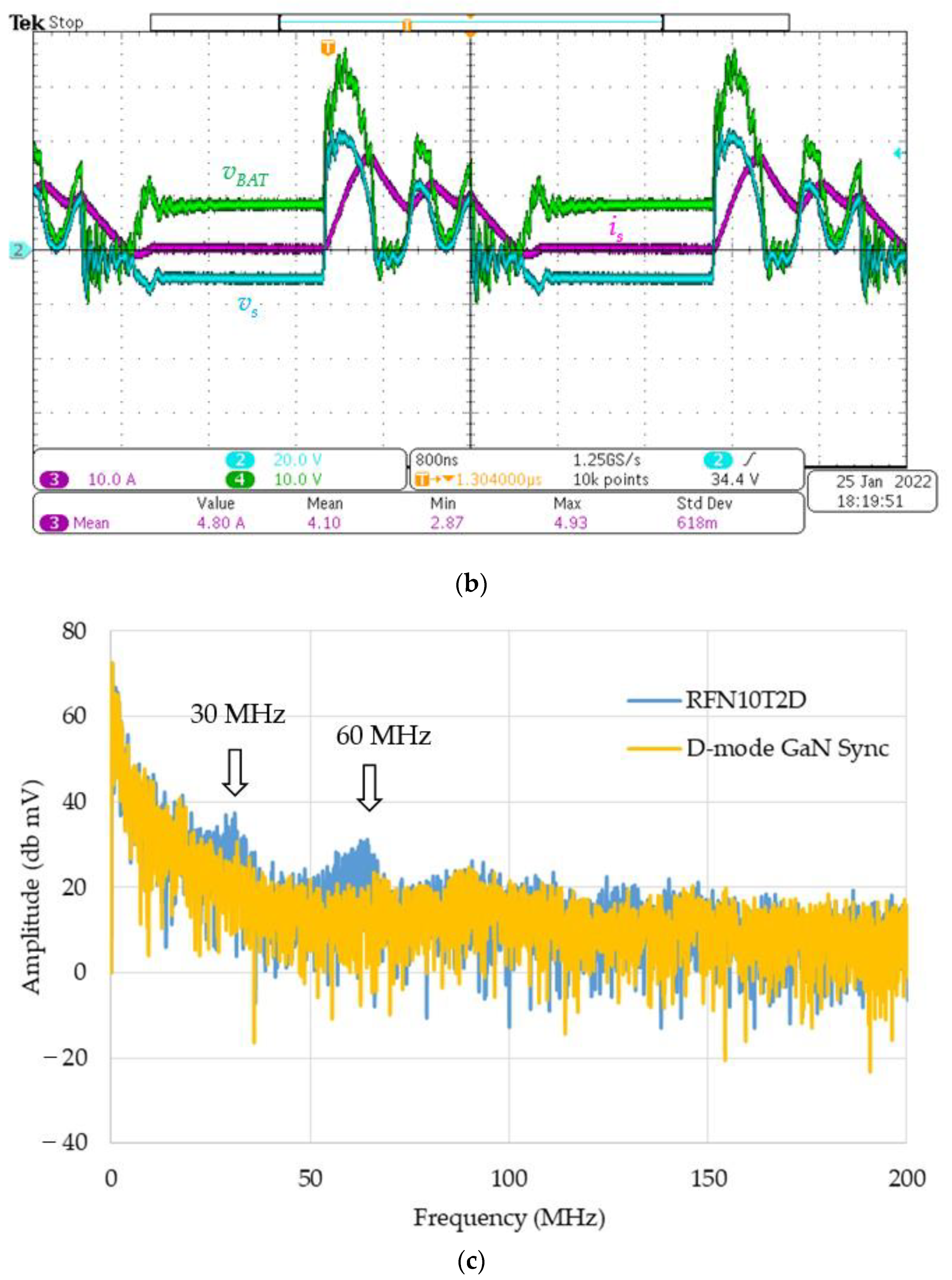
- The zero-voltage capacitance of the conventional diode is low, which causes much oscillation noise which becomes a burden to the EMI filter. The GaN HEMT will present a smoother switching response in the voltages compared to the rectifier diode. The switching ringing during the diode turn-off as well as the inductor charging period are most benefited by the D-Mode GaN HEMT synchronous rectifier.
4. Simulation and Experimental Results
4.1. SPICE Simulation of the D-Mode GaN HEMT Synchronous Rectifier
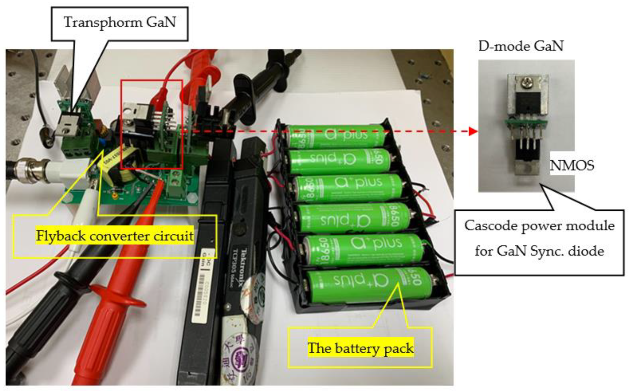
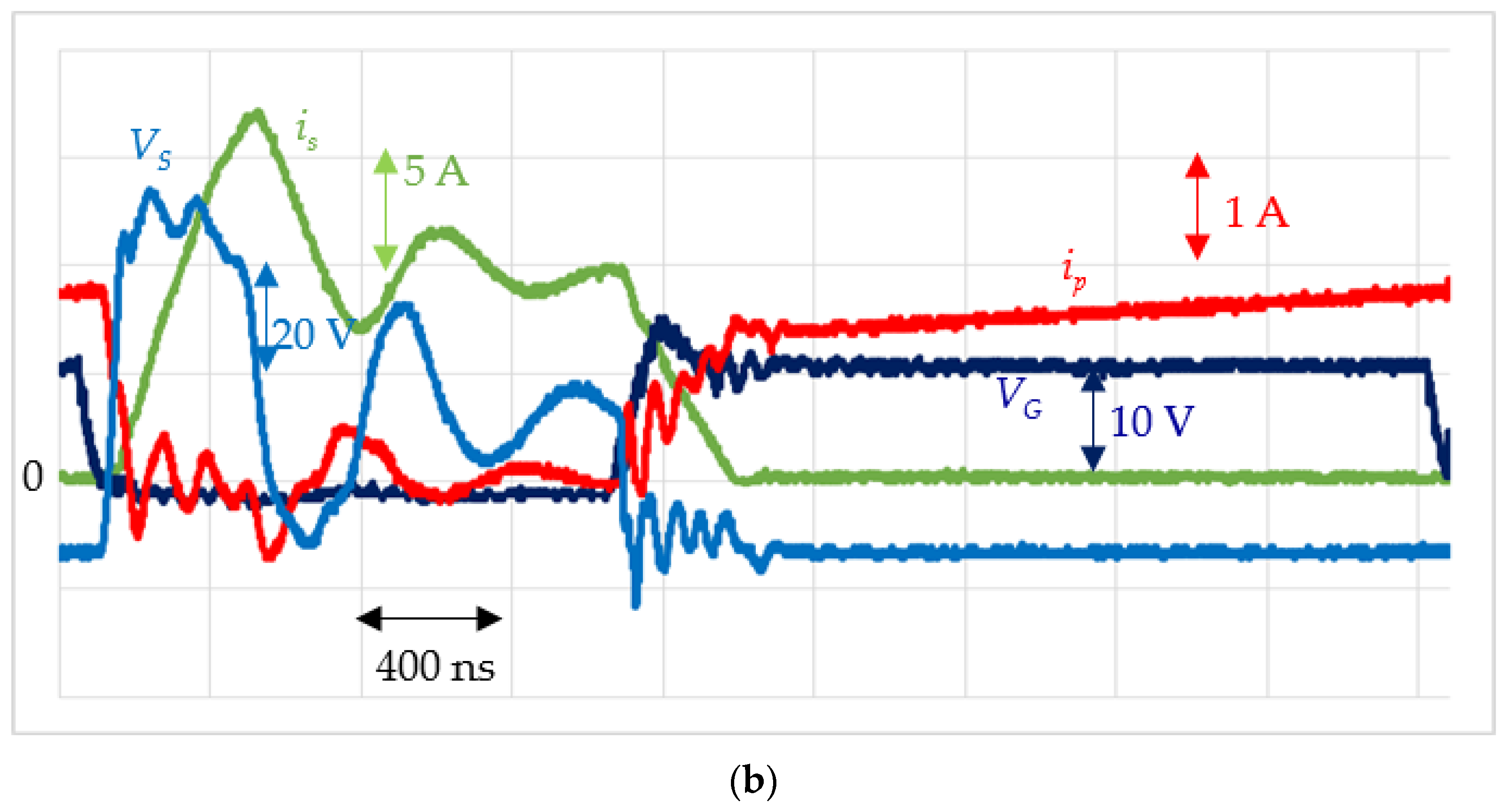
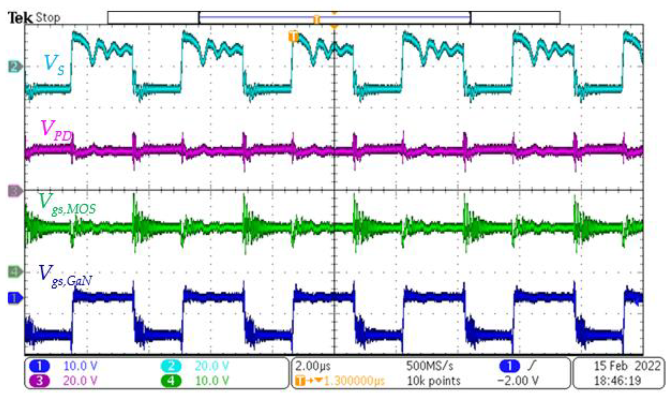
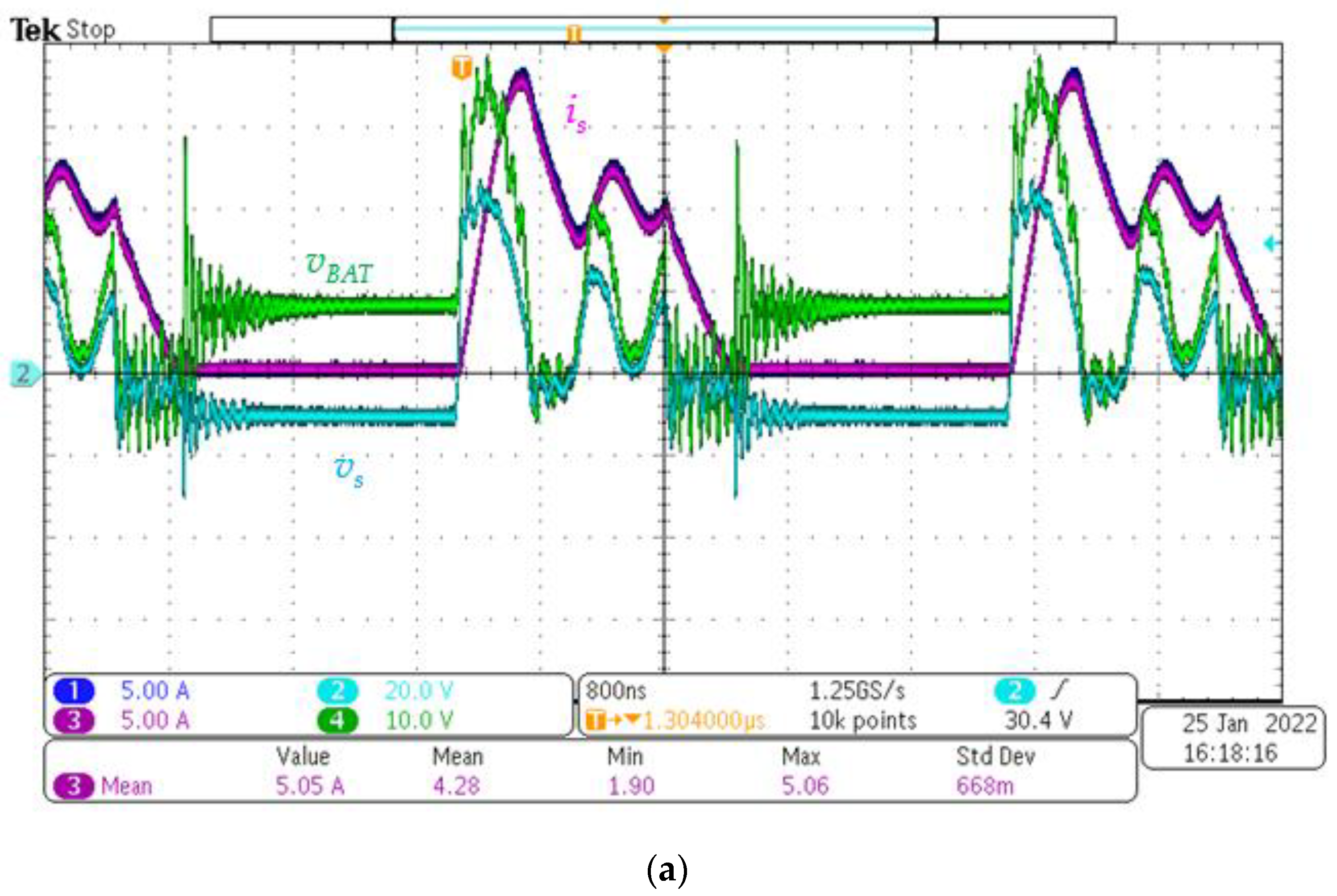
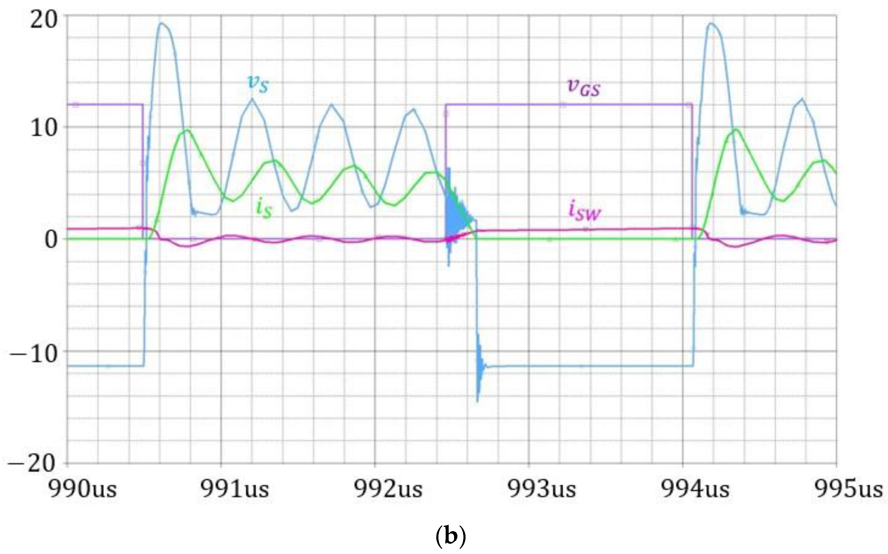
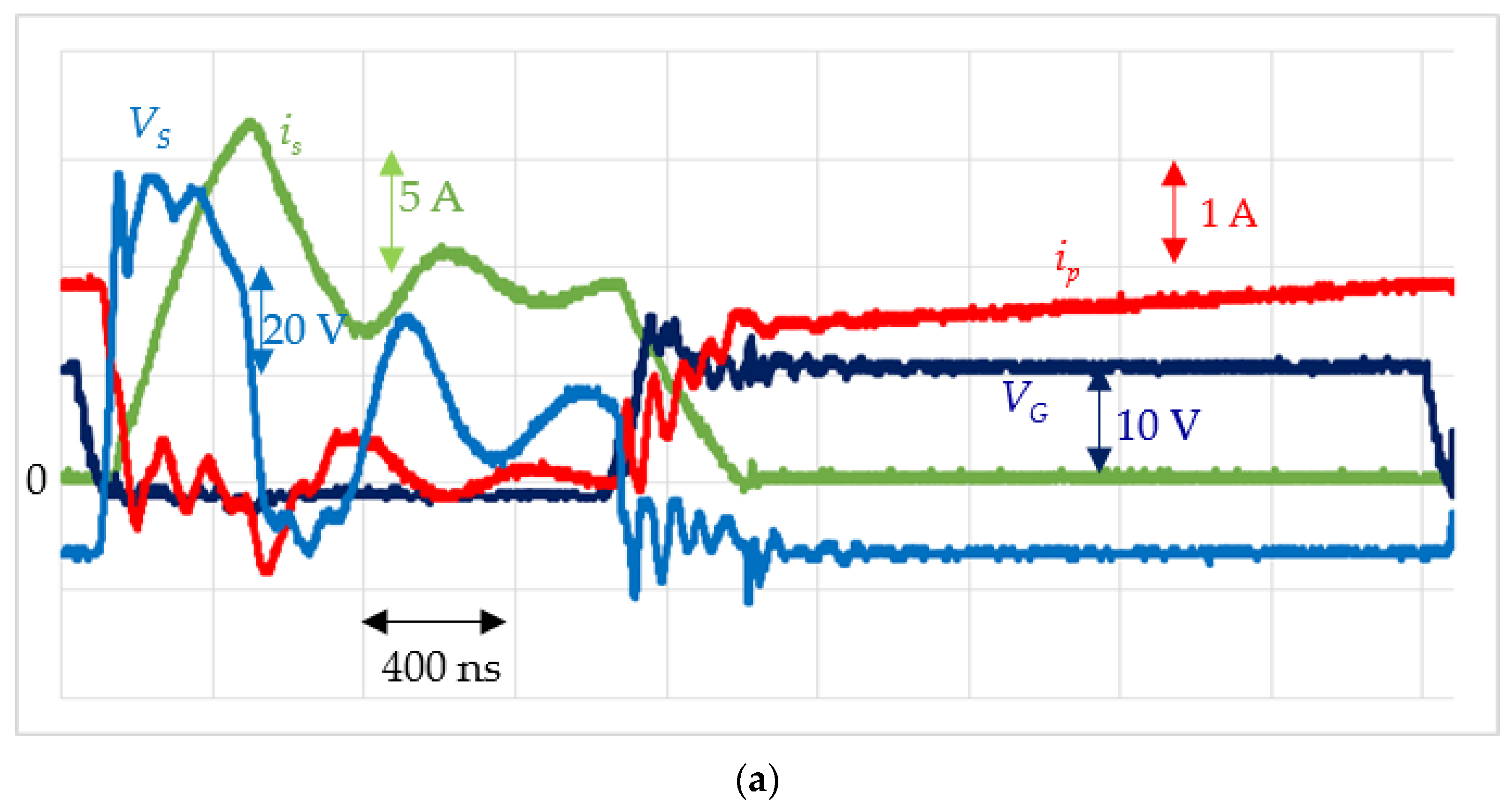
4.2. Experimental Result
5. Discussion
6. Conclusions
Author Contributions
Funding
Institutional Review Board Statement
Informed Consent Statement
Data Availability Statement
Acknowledgments
Conflicts of Interest
References
- Ramos-Paja, C.A.; Bastidas-Rodriguez, J.D.; Saavedra-Montes, A.J. Design and Control of a Battery Charger/Discharger Based on the Flyback Topology. Appl. Sci. 2021, 11, 10506. [Google Scholar] [CrossRef]
- Guo, X.; Geng, J.; Liu, Z.; Xu, X.; Cao, W. A Flyback Converter-Based Hybrid Balancing Method for Series-Connected Battery Pack in Electric Vehicles. IEEE Trans. Veh. Technol. 2021, 70, 6626–6635. [Google Scholar] [CrossRef]
- Imtiaz, A.M.; Khan, F.H. “Time Shared Flyback Converter” Based Regenerative Cell Balancing Technique for Series Connected Li-Ion Battery Strings. IEEE Trans. Power Electron. 2013, 28, 5960–5975. [Google Scholar] [CrossRef]
- Yang, Y.-D.; Hu, K.-Y.; Tsai, C.-H. Digital Battery Management Design for Point-of-Load Applications with Cell Balancing. IEEE Trans. Ind. Electron. 2019, 67, 6365–6375. [Google Scholar] [CrossRef]
- Jeng, S.L.; Peng, M.T.; Hsu, C.Y.; Chieng, W.H.; Shu, J.P. Quasi-Resonant Flyback DC/DC Converter Using GaN Power Transistors. World Electr. Veh. J. 2012, 5, 567–573. [Google Scholar] [CrossRef] [Green Version]
- Mauromicale, G.; Raciti, A.; Rizzo, S.A.; Susinni, G.; Fusillo, F.; Palermo, A.; Scrimizzi, F. Efficiency of state-of-the-art GaN devices in a synchronous-rectifier buck converter. In Proceedings of the IECON 2019—45th Annual Conference of the IEEE Industrial Electronics Society, Lisbon, Portugal, 14–17 October 2019; pp. 1726–1731. [Google Scholar]
- Ho, G.K.Y.; Fang, Y.; Pong, B.M.H.; Hui, R.S.Y. Printed circuit board planar current transformer for GaN active diode. In Proceedings of the 2017 IEEE Applied Power Electronics Conference and Exposition (APEC), Tampa, FL, USA, 26–30 March 2017; pp. 2549–2553. [Google Scholar]
- Paolucci, M.; Green, P.B. Benefits of GaN e-Mode HEMTs in Wireless Power Transfer—GaN Power Devices in Resonant Class D and Class E Radio Frequency Power Amplifiers. October 2018. Rev 1.0. Infineon, White Paper. Available online: https://www.infineon.com/wirelesscharging (accessed on 17 October 2018).
- Zhang, Y.; Yang, F. Maximizing the Performance of GaN with Ideal Diode Mode; Texas Instruments Application Report; Texas Instruments: Dallas, TX, USA, 2020. [Google Scholar]
- Peftitsis, D.; Rabkowski, J.; Nee, H.-P. Self-Powered Gate Driver for Normally ON Silicon Carbide Junction Field-Effect Transistors Without External Power Supply. IEEE Trans. Power Electron. 2012, 28, 1488–1501. [Google Scholar] [CrossRef]
- Ishibashi, T.; Okamoto, M.; Hiraki, E.; Tanaka, T.; Hashizume, T.; Kikuta, D.; Kachi, T. Experimental validation of normally-on GaN HEMT and its gate drive circuit. IEEE Trans. Ind. Appl. 2014, 51, 2415–2422. [Google Scholar] [CrossRef]
- Wu, C.-C.; Liu, C.-Y.; Anand, S.; Chieng, W.-H.; Chang, E.-Y.; Sarkar, A. Comparisons on Different Innovative Cascode GaN HEMT E-Mode Power Modules and Their Efficiencies on the Flyback Converter. Energies 2021, 14, 5966. [Google Scholar] [CrossRef]
- Sun, B. Does GaN Have a Body Diode? Understanding the Third Quadrant Operation of GaN; Application Report-SNOAA36; Texas Instruments: Dallas, TX, USA, 2019. [Google Scholar]
- Asad, M.; Singha, A.K.; Rao, R.M.S. Dead Time Optimization in a GaN-Based Buck Converter. IEEE Trans. Power Electron. 2021, 37, 2830–2844. [Google Scholar] [CrossRef]
- Chiu, P.K.; Wang, P.Y.; Li, S.T.; Chen, C.J.; Chen, Y.T. A GaN driver IC with novel highly digitally adaptive dead-time control for synchronous rectifier buck converter. In Proceedings of the 2020 IEEE Energy Conversion Congress and Exposition (ECCE), Detroit, MI, USA, 11–15 October 2020; pp. 3788–3792. [Google Scholar]
- Xue, L.; Zhang, J. Highly Efficient Secondary-Resonant Active Clamp Flyback Converter. IEEE Trans. Ind. Electron. 2017, 65, 1235–1243. [Google Scholar] [CrossRef]
- Tang, L.C.; Jeng, S.L.; Chang, E.Y.; Chieng, W.H. Variable-Frequency Pulse Width Modulation Circuits for Resonant Wireless Power Transfer. Energies 2021, 14, 3656. [Google Scholar] [CrossRef]
- Wu, C.-C.; Liu, C.-Y.; Wang, G.-B.; Shieh, Y.-T.; Chieng, W.-H.; Chang, E.Y. A New GaN-Based Device, P-Cascode GaN HEMT, and Its Synchronous Buck Converter Circuit Realization. Energies 2021, 14, 3477. [Google Scholar] [CrossRef]
- Kumar, R.; Wu, C.-C.; Liu, C.-Y.; Hsiao, Y.-L.; Chieng, W.-H.; Chang, E.-Y. Discontinuous Current Mode Modeling and Zero Current Switching of Flyback Converter. Energies 2021, 14, 5996. [Google Scholar] [CrossRef]
- Zhan, H.; Wu, H.; Muhammad, M.; Lambert, S.; Pickert, V. Combining electric vehicle battery charging and battery cell equalisation in one circuit. IET Electr. Syst. Transp. 2021, 11, 377–390. [Google Scholar] [CrossRef]
- Meng, X.Z.; Li, C.Y.; Meng, T.; An, Y.H. Analysis and Design of Transformer Windings Schemes in Multiple-Output Flyback Auxiliary Power Supplies with High-Input Voltage. J. Power Electron. 2019, 19, 1122–1132. [Google Scholar]
- Liu, C.-Y.; Wang, G.-B.; Wu, C.-C.; Chang, E.Y.; Cheng, S.; Chieng, W.-H. Derivation of the Resonance Mechanism for Wireless Power Transfer Using Class-E Amplifier. Energies 2021, 14, 632. [Google Scholar] [CrossRef]
- Weng, Y.-C.; Wu, C.-C.; Chang, E.Y.; Chieng, W.-H. Minimum Power Input Control for Class-E Amplifier Using Depletion-Mode Gallium Nitride High Electron Mobility Transistor. Energies 2021, 14, 2302. [Google Scholar] [CrossRef]
- Wu, C.C.; Jeng, S.L. Comparison of Parasitic Capacitances of Packaged Cascode Gallium Nitride Field-effect Transistors. Sens. Mater. 2018, 30, 453–461. [Google Scholar]
- Kolar, J.W.; Krismer, F.; Lobsiger, Y.; Mühlethaler, J.; Nussbaumer, T.; Miniböck, J. Extreme Efficiency Power Electronics. In Proceedings of the International Conference of Integrated Power Electronics Systems (CIPS 2012), Nuremberg, Germany, 6–8 March 2012; pp. 1–22. [Google Scholar]
- Shieh, Y.-T.; Wu, C.-C.; Liu, C.-Y.; Chieng, W.-H.; Su, Y.-S.; Jeng, S.-L. Modelling of Parallel Lithium Battery Charging. Energies 2022. submitted. [Google Scholar]


| Symbol | Unit | Original | Value |
|---|---|---|---|
| COSS | pF | Measurement | 200 @ VDS = 72 V |
| VDD | V | Measurement | 72 V |
| vBAT | V | Measurement | 7 |
| a | Measurement | 6 | |
| VTH,Ds | V | RFN10T2D | 0.5 V |
| ω1 | Mrad | Equation (5) | 3.5 |
| tD,riseip(0) | nC | Equation (7) | 23 |
| Symbol | Unit | Original | Value |
|---|---|---|---|
| CB | μF | Measurement | 1 |
| a | Measurement | 6 | |
| RBs | Ω | Measurement | 33 |
| RS | Ω | Measurement | 0.55 |
| LSl | nH | Measurement | 270 |
| tsnubber, T2 | ns | Equation (16) | 300 |
| Symbol | Unit | Original | Value |
|---|---|---|---|
| LPl | uH | RLC meter | 9.97 |
| f2 = ω2/2π | MHz | Equation (18) | 3.6 |
| δ | Input | 45% | |
| IBCH | A | Equation (20) | 6 |
| Symbol | Unit | Original | Value |
|---|---|---|---|
| tD, all | ns | Equation (26) | 100 |
| Symbol | Unit | Original | Value |
|---|---|---|---|
| Cj0 | pF | Data sheet | 15 |
| f3 = ω3/2π | MHz | Equation (29) | 60 |
| ξ3 | Damping ratio | Equation (30) | 0.002 |
| Symbol | Unit | Description | Value | vDS | |
|---|---|---|---|---|---|
| 0 V | 800 V | ||||
| Vgs,GaN_ON | V | Turn-on voltage | −7 | ||
| CDS | pF | Parasitic capacitance | 40 | 30 | |
| CGD | pF | Parasitic capacitance | 220 | 20 | |
| CGS | pF | Parasitic capacitance | 100 | 115 | |
| Symbol | Unit | Original | Value |
|---|---|---|---|
| CP | nF | Peak detector capacitor | 1 |
| DP | Power module diode 1 | BAV170 | |
| DM | Power module diode 2 | 1N4007 | |
| CPD | nF | Peak detector capacitor | 100 |
| RPD | Ω | Peak detector resistor | 33 |
| DPD | Peak detector diode | 1N4007 | |
| IC | Gate drive | LM5114B | |
| RG,n | Ω | Gate drive | 27 |
| RG,p | Ω | Gate drive | 30 |
| Symbol | Unit | Description | Value |
|---|---|---|---|
| Rp | mΩ | Primary winding resistance | 1 |
| Cp | pF | Primary parasitic capacitance | 10 |
| Lp1 | nH | Primary parasitic inductance | 300 |
| Lp | μH | Primary winding inductance | 400 |
| Ls | μH | Secondary winding inductance | 10.27 |
| Cs | pF | Secondary parasitic capacitance | 10 |
| Ls1 | nH | Secondary parasitic inductance | 235 |
| k | - | Coupling coefficient | 0.987 |
| Time | Equation Number | Analysis | Simulation |
|---|---|---|---|
| tD,rise (ns) | (7) | 28 | 34 |
| tsnubber (ns) | (16) | 166 | 137 |
| tBCH (ns) | (21) | 1770 | 1786 |
| tD,fall (ns) | (26) | 100 | 89 |
| tLCH (ns) | (32) | 1390 | 1510 |
| Parameter | Type | Value |
|---|---|---|
| Power switch | - | |
| Snubber diode (DB) | 1N4007 | - |
| Magnetizing inductor (Lp, Ls) | - | 400 μH, 10.27 μH |
| Leakage inductor (LPl, LSl) | - | 9.97 μH, 0.27 μH |
| Snubber capacitor (CB) | Ceramic capacitor | 3300 pF |
| Snubber resistance (RBs) | Carbon film resistor | 45 Ω |
| Turn ratio | - | 6 |
| Time | Equation Derived | Diode (RFN10T2D) | Synchronous Rectifier (D-Mode GaN HEMT) |
|---|---|---|---|
| tD,rise (ns) | 11 | 30 | 30 |
| tsnubber (ns) | 216 | 350 | 350 |
| tBCH (ns) | 1140 | 1058 | 1041 |
| tD,fall (ns) | 133 | 440 | 420 |
| tLCH (ns) | 1667 | 1693 | 1730 |
Publisher’s Note: MDPI stays neutral with regard to jurisdictional claims in published maps and institutional affiliations. |
© 2022 by the authors. Licensee MDPI, Basel, Switzerland. This article is an open access article distributed under the terms and conditions of the Creative Commons Attribution (CC BY) license (https://creativecommons.org/licenses/by/4.0/).
Share and Cite
Shieh, Y.-T.; Liu, C.-Y.; Wu, C.-C.; Chieng, W.-H.; Chang, E.-Y. Flyback Converter Using a D-Mode GaN HEMT Synchronous Rectifier. Energies 2022, 15, 3197. https://doi.org/10.3390/en15093197
Shieh Y-T, Liu C-Y, Wu C-C, Chieng W-H, Chang E-Y. Flyback Converter Using a D-Mode GaN HEMT Synchronous Rectifier. Energies. 2022; 15(9):3197. https://doi.org/10.3390/en15093197
Chicago/Turabian StyleShieh, Yueh-Tsung, Ching-Yao Liu, Chih-Chiang Wu, Wei-Hua Chieng, and Edward-Yi Chang. 2022. "Flyback Converter Using a D-Mode GaN HEMT Synchronous Rectifier" Energies 15, no. 9: 3197. https://doi.org/10.3390/en15093197
APA StyleShieh, Y.-T., Liu, C.-Y., Wu, C.-C., Chieng, W.-H., & Chang, E.-Y. (2022). Flyback Converter Using a D-Mode GaN HEMT Synchronous Rectifier. Energies, 15(9), 3197. https://doi.org/10.3390/en15093197