1. Introduction
Battery-powered devices have become widespread in recent decades, successfully replacing older technologies in many sectors, but with the drawback of requiring regular energy replenishment. The recharge technologies used for these devices have undergone various degrees of development over time in terms of charging speed, efficiency, and type of transmission. The last few years have seen the development of wireless power transmission techniques, in which the power is transferred without the use of wired conductors. There is, in fact, a rising interest in wireless power transfer (WPT), not only for consumer electronics but also for medical instruments, industrial devices, satellites [
1,
2,
3,
4,
5,
6], and electric vehicles (EV), including stationary and moving wireless charging [
7,
8,
9,
10,
11]. A WPT system offers many advantages, which include insulation from the environment, higher safety due to the absence of exposed live metal parts, and superior flexibility and ease of use for the end-user.
Different WPT systems and technologies have been developed over the years, including the Qi from the Wireless Power Consortium (WPC), a wireless charging standard that provides 5–15 W [
12], and other WPC standards such as the Ki Cordless Kitchen, delivering up to 2 kW to kitchen cordless appliances, the Light Electric Vehicle (LEV) standard for e-bikes and scooters, and the “Industry” standard for wireless charging of robots, automatic guided vehicles, and other industrial machinery [
13]. Other commercial technologies include those from the AirFuel Alliance in the “Resonant” variant, which uses magnetic resonance technology to provide alignment-free charging to power multiple devices simultaneously, or the Radio Frequency (RF) version that enables charging of multiple devices simultaneously within a volume [
14].
The WPT systems can be classified into far-field and near-field, according to the transmission distance [
15]. Usually, far-field transmission is deployed by using lasers or microwaves and a direct transmission path [
16]. It is mainly designed for low-power applications, also because of the risk of radiofrequency exposure of the human body to levels above the safety limit [
17]. On the other hand, the near-field transmission allows the achievement of higher efficiencies and does not represent a safety concern; popular near-field WPT systems are inductive or capacitive power transfer and permanent magnet coupling (PMC) [
18]. Near-field transmissions include short- and medium-range transmissions, the former with operating ranges of few centimeters and generally based on the magnetic coupling of two coils. At higher distances, the use of intermediate stronger coupled resonant coils can improve the efficiency [
19]. Short-range applications usually have operating frequencies in the range of dozens of kHz up to a few MHz, and generally, the power dissipation in the power inverter increases with the operating frequency due to the higher switching losses.
Most WPT applications are powered by a DC-link and use resonant circuits driven by inverters [
20,
21] at the appropriate resonant frequency. Typically, WPT systems use MOSFETs in silicon (Si) as switching devices in the DC-AC conversion circuits. However, Gallium Nitride (GaN) power devices have been emerging in the global semiconductor market for several years now as a viable alternative to silicon-based devices to reduce energy dissipation. GaN devices, in particular, find wide and advantageous applications in systems operating at relatively low voltages, below 150 V; by comparison, silicon carbide (SiC) devices have definitely conquered the market for higher power applications at voltages above 600 V [
22,
23].
The latest GaN High Electron Mobility Transistors (HEMTs) are advertised as being able to allow the design of power conditioning circuits with dissipation and dimensions that are more than halved compared to Si. Wireless power transmission applications can therefore benefit from the GaN technology, which enables the design of systems operating at higher frequencies than Si-based ones. Compared to silicon, GaN HEMTs require, for the same on-state resistance value, up to ten times less gate charge for turn-on, implying lower losses and virtually negligible turn-off times [
24]. The parasitic output capacitance is also about ten times lower than that of comparable Super-Junction MOSFETs. In addition, GaN HEMTs also have significant advantages over SiC MOSFETs, with up to four times shorter turn-on time and halved turn-off time [
25].
In some cases, GaN devices have already been used to build WPT systems operating at frequencies considerably higher than those normally used in inductively coupled systems, i.e., those designed according to Qi or other WPC standards. A significant case in point is the resonant coupling circuits of the AirFuel standard that operate at 6.78 MHz.
In terms of circuit topologies, highly efficient Class E amplifiers are frequently used in low and medium power WPT systems [
26,
27,
28,
29,
30]. The single-switch structure allows high efficiency at high operating switching frequencies, and the parasitic output capacitance of the switching device can be advantageously used to achieve soft switching, such as zero-voltage switching (ZVS) at turn on, thus significantly reducing stresses and switching losses. This topology allows controlling the output power by controlling the duty cycle or the switching frequency. This high-power amplifier topology is probably the preferred choice when the peak operating voltage is far enough from the technological limitations of the switching devices (breakdown voltage,
VBD) since the peak voltages occurring at the load are up to 3.5 times the DC bias voltage of the circuit. As a result, it provides less power than other resonant inverters with the same voltage and current stresses.
For medium- to high-power WPT systems, the class D topology is more common [
31,
32]. The class D inverter employs a resonant tank and two or four switches in a half-bridge or full-bridge configuration. This topology allows the full potential of the switching devices to be exploited in conjunction with the power supply circuit since the peak voltage is strictly bound to the value of the bias voltage. The peak voltage in the class D full-bridge is twice as high as the DC supply voltage, which is convenient for WPT applications with low DC supply. The two-switches version has lower voltage stress across the switch because the peak voltage equals the DC supply. With the class D topology, it is easier to reduce the switching losses in the case of a resonant load in series, since the sinusoidal nature of the current can be appropriately exploited to avoid full current switching. If the frequency operating range of a Class D amplifier is to be extended, advantages can be realized from the use of fast switching devices, such as GaN-based Field Effect Transistors (FETs). GaN-FETs have been used successfully both in 13 MHz Class E topologies [
33] and in 6.78 MHz Class D topologies [
34], where a circuit capable of transmitting power up to several tens of watts with a peak transmission efficiency of 73% at a power of 44 W and a distance of 5 cm was shown.
Several strategies are able to be used to control a high-efficiency WPT circuit, including adjusting the switching frequency, tuning the capacitive network through a switch matrix [
35], or controlling the equivalent load by varying the duty cycle of a converter on the receiver circuit [
34,
36]. In [
37], a 6.78 MHz class E WPT system with GaN devices was realized, which includes a loop control called automatic matching-point-searching (AMPS) that allows zero-voltage switching to minimize power consumption and makes the system efficiency independent of load variations.
As regards the antenna coils, various compensation networks are possible for the resonant circuits. An LC resonator is usually used, and the compensation capacitor can be placed either in parallel or series with the inductive coil. The series compensation has the characteristic of a voltage source, whereas the parallel compensation has the characteristic of a current source. The basic compensation networks for primary and secondary circuits are series–series (SS), series–parallel (SP), parallel–series (PS), and parallel–parallel (PP) topologies [
7,
18,
38]. In addition, other topologies such as LCC and LCL have been developed to improve the system performance and achieve more flexible operations. SS, the topology selected for this research, is the most popular for practical application due to its high tolerance to system parameters and lack of reflected reactance, which simplifies the system design since the resonant frequency is not affected by the distance between coils and load variations [
39].
The overall efficiency, i.e., the DC-to-DC conversion efficiency, of a WPT system depends on multiple factors, including the efficiency of the inverter feeding the resonant circuit. As previously mentioned, GaN-based WPT circuits have already been developed in the literature with operating frequencies of several MHz [
33,
34,
37]; however, there are no direct Si vs. GaN performance comparisons at lower frequency ranges. The aim of this study was to verify the feasibility and advantages that may derive from the use of the GaN technology in the design of a system operating at frequencies between a few hundred kHz up to a few MHz, with electronic, mechanical, and thermal characteristics suitable for a wide range of applications.
This study focused on the evaluation of a WPT circuit based on either GaN HEMTs or conventional Si MOSFETs; to this end, the overall performances of two equivalent circuits based on the two technologies were compared at frequencies of the order of the MHz. Several tests were carried out under different operating conditions, such as varying loads, frequencies, dead-time, supply voltages, and distance between the transmitting and receiving coils. Moreover, the theory and design choices regarding the WPT circuit, the coils, and the resonant network are also discussed.
Two specific custom WPT boards were designed and realized, both with equivalent topology and based on a full-bridge configuration: one with GaN and one with conventional Si switching devices. The boards were designed to allow high flexibility of use, both in terms of control modes and driving parameters of the active devices of the bridge, and in terms of inductive loads that can be driven. Moreover, they can operate in a wide range of switching frequencies, allowing them to be used for close- and mid-range wireless power transmission tests.
The paper is organized as follows.
Section 2 includes a theoretical overview of a WPT system and a description of the realized test circuit and measurement setup.
Section 3 reports the performance comparison between the GaN and the Si-based solutions. Finally,
Section 4 comprises a discussion and the conclusions of the work.
2. Description of the WPT System
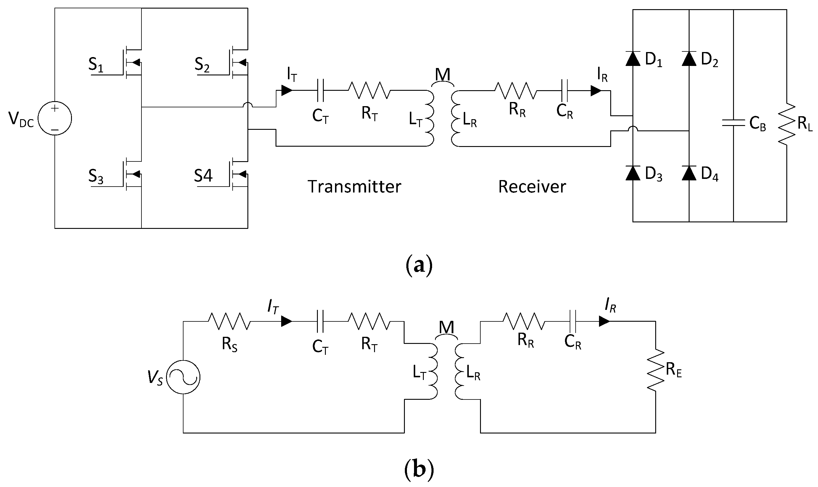
For the aim of this study, two complete WPT transmission systems, one based on MOSFETs in Si and the other using HEMTs in GaN, were designed and realized. An in-depth comparison between these two solutions follows, aimed at highlighting the advantages and disadvantages of each of them. The two specific custom boards are both based on a full-bridge configuration (
Figure 1a). They are characterized by a high flexibility of use, both in terms of control modes and parameters of the active devices of the bridge (voltages, phase shifts, dead-time, etc.), and in terms of inductive loads that can be driven, and allow operation at frequencies higher than one mega-Hertz. This configuration allows multiple control modes of the switches, thus improving the operating range as the load condition changes.
The system is completed by two coil antennas with series capacitances, forming the resonant primary and secondary circuits, and by a diode bridge rectifier at the secondary that outputs a DC voltage on the load.
2.1. Theory of Operation
The system uses an LC resonant circuit in SS configuration, one of the most popular compensation networks in practical applications, which is easy to set up as the capacitance value does not depend on the coupling coefficient and hence on the distance between the antennas. As shown in
Figure 1a, at the primary the resonant network is composed of
LT and
CT, representing the coil inductance and the capacitance, the latter including both the distributed capacitance of the coil and the externally added compensation capacitance. At the secondary,
LR and
CR represent the coil inductance and compensation capacitance, and
RL is the load resistor.
RT and
RR represent the losses in the transmitter and receiver resonators, including the coil resistance and the capacitors’ series resistance.
The equivalent circuit is shown in
Figure 1b, where
is the equivalent sinusoidal voltage source generated from the full-bridge inverter,
is its internal resistance, depending on the MOSFET characteristics, and
is the equivalent load resistance including the effect of the rectifier. In the design of a WPT system, the equivalent circuit model allows one to easily derive currents and voltages through the coils and capacitors, and therefore to estimate the required component ratings. For convenience, only the fundamental component of the periodic signals is considered in the subsequent analysis; this approximation is fairly accurate for a system working near the resonance frequency [
39]. The resonant frequency for the transmitter and receiver resonators is:
and we can express the mutual inductance
M between the transmitter and the receiver as a function of the coupling coefficient
k and the inductance of the two coils:
The impedances of the primary and secondary sides for the series compensation network are, respectively:
where
and
are, respectively, the effective series resistance of the transmitting and receiving sections.
At the resonance condition ω0, the reactive impedance becomes zero and the impedance of the primary and secondary sides for series compensation topology are respectively and . In this condition, voltage and current are in phase and, as a consequence, the inverter uses the hard-switching technique that can cause higher switching losses; practically, the operating switching frequency is slightly shifted away from the nominal resonant frequency to achieve zero current or zero voltage switching.
From
Figure 1b, the system can be expressed as follows:
where the bold letters represent the phasors of the respective symbols. From this, the two currents can be derived as follows:
The input and the output powers on the equivalent load resistor are:
and the inductive resonant link transfer efficiency can be calculated as:
From these equations, it is possible to note that the input power, output power, and efficiency depend on the mutual inductance, and hence on the coupling factor between the two coils. The input power is higher when the mutual inductance is small and hence the two coils are loosely coupled; this represents the worst operating condition with the maximum currents in the transmitter resonator, which also approximatively corresponds to the peak current across the inverter switches.
The output power varies with the coupling factor; to keep a constant output power when the distance increases, the equivalent load resistance should be reduced, increasing the resonator current.
Generalizing, when a system works on different coupling conditions due to variable distance or misalignment of the coils, the low value of the coupling factor k represents the worst operating conditions, with the highest currents and voltages in the resonators. This condition has to be considered when sizing components.
The efficiency depends on the resonant operating frequency. For a given coil structure, the resonant frequency can be adjusted by varying the value of the compensation capacitor. Without considering the conversion efficiency of the full-bridge inverter, the maximum transfer efficiency is achieved when the system operates at higher resonant frequencies. However, the output power is maximum at a certain optimal frequency and decreases if the frequency is increased further. Operating at higher frequencies also allows the maintenance of high efficiency when the coils are poorly coupled, and therefore can improve the system performance at higher distances.
Figure 2 shows the WPT system behavior, according to Equations (7)–(9), as a function of the resonant frequency for a system with
LT =
LR = 1 μH,
RT =
RR = 0.6 Ω,
VS = 12 V, for two different values of load
RE and coupling coefficient
k.
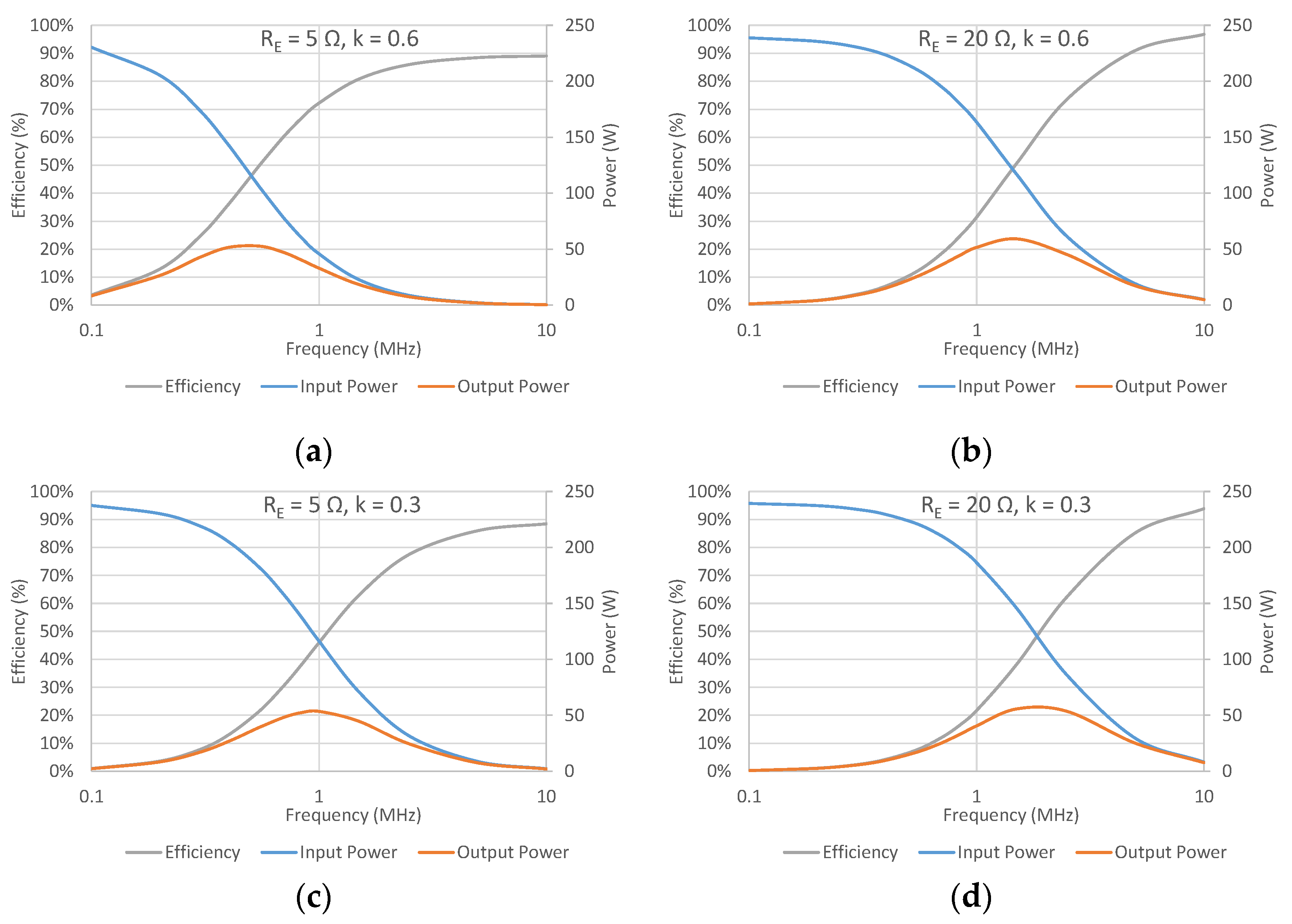
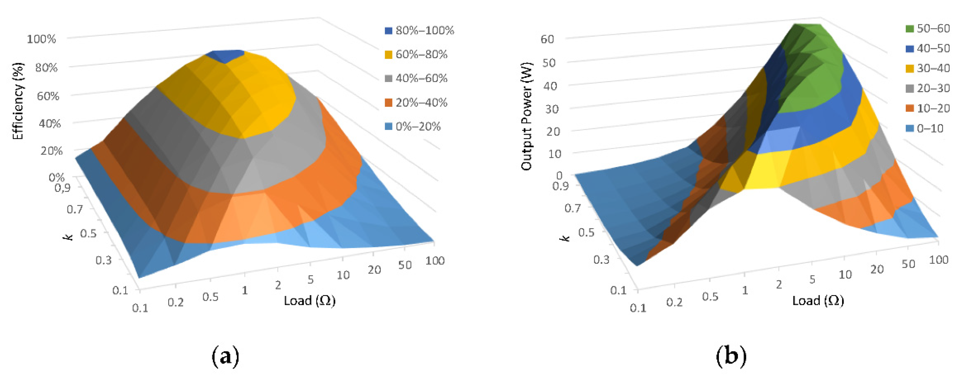
Figure 3 shows the system efficiency and output power variation versus the load resistance (
RE) and coupling coefficient
k for the same configuration, at a resonant frequency of 1 MHz. Both efficiency and output power depend on the value of the load resistance as shown in Equations (8) and (9); from these equations, it is possible to derive the optimal load resistor necessary to achieve maximum efficiency and maximum output power conditions. An impedance matching network on the receiving stage can be used to set the equivalent load resistance to the optimal value; this can be achieved by making use of a DC-DC converter, such as a buck converter following the diode bridge rectification, which provides an adjustable impedance by controlling the duty cycle.
The power losses caused by the switching devices of the inverter and rectifier circuits should be also considered to obtain the overall efficiency. The power loss of a switching device consists of two main components, namely the switching losses and conduction losses. For a MOSFET, the conduction losses are caused by the drain-source resistance RDS(on) and do not depend on frequency, whereas the switching losses have a linear dependence on the operating frequency and affect the overall efficiency of the system for very high frequencies. These losses can be modeled as part of the total equivalent series resistances on the primary and secondary of the equivalent circuit.
Ultimately, increasing the resonant frequency can improve the wireless transfer efficiency and the power transmission distance. However, the increment of the operating frequency increases the switching losses of the MOSFETs and can affect the system’s reliability. The use of GaN devices can help maintain low switching losses because of their very low turn-on and turn-off times. Moreover, the adoption of soft-switching techniques can be helpful to reduce the switching losses on the devices by shifting the phase between voltage and current; this can be done by operating at a frequency slightly shifted from the nominal resonant frequency [
40].
2.2. WPT Boards
The transmission system has a modular design with two stacked boards that accommodate, respectively, the power subsystem with four switches in a full-bridge configuration and the power supply rails, and a logic subsystem with the microcontroller that controls the system. The system architecture is derived from the open-source platform presented in [
41].
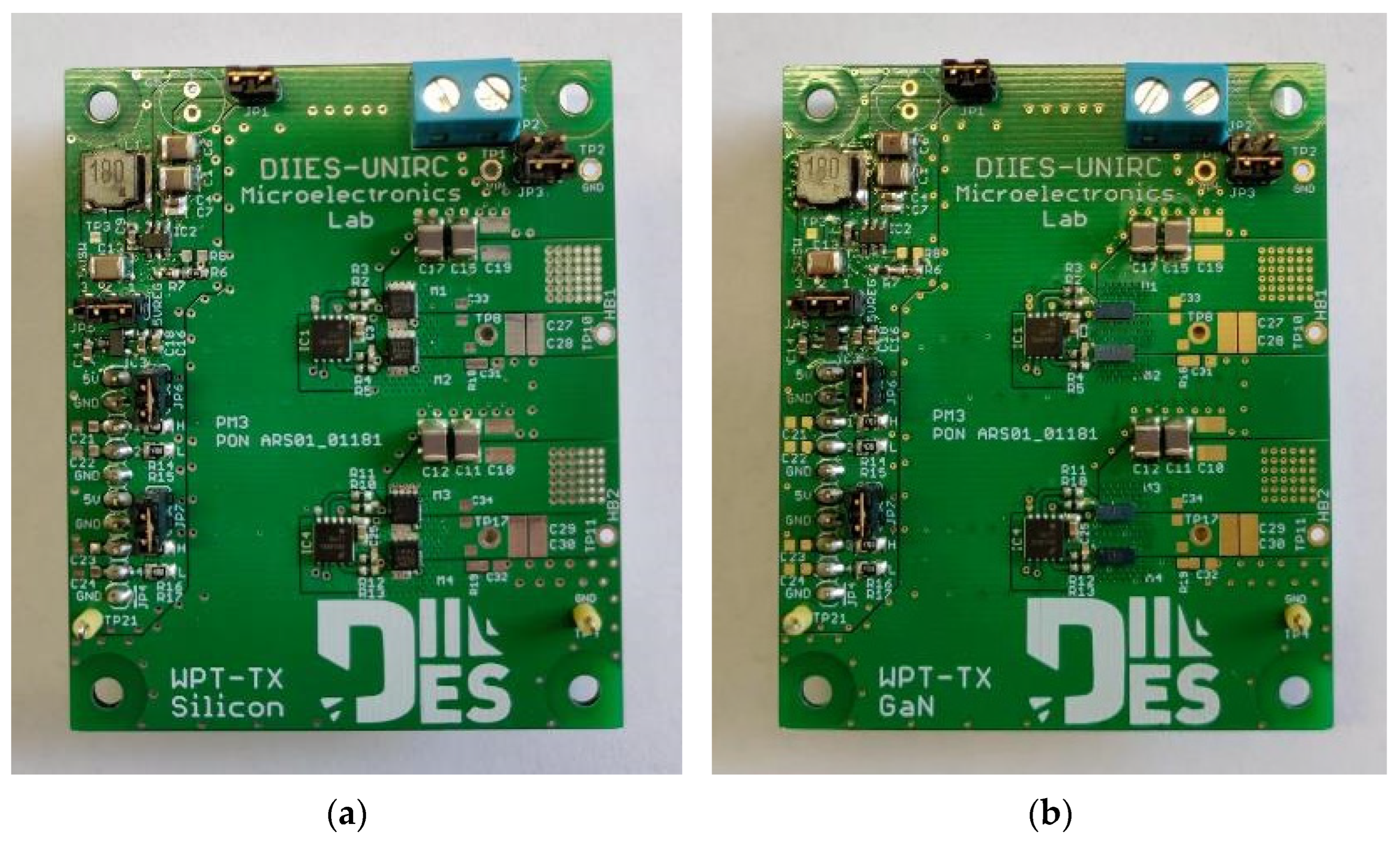
The designed GaN board is based on EPC2001C devices [
42] characterized by a maximum drain-source voltage (V
DS) of 100 V, an R
DS(on) of 7 mΩ, and a maximum current of 36 A. The switches are controlled via the LM5113 driver from Texas Instrument [
43]. The Si-based board includes SiS892DN MOSFETs [
44], with characteristics comparable to those of the GaN device, i.e., a maximum V
DS of 100 V and a maximum current of 30 A. The selected silicon device provides low input and output capacitance, comparable with those of the GaN device. However, the R
DS(on) is higher (34 mΩ) due to the different physical properties of the two materials; the rest of the components are identical to those of the GaN-based board.
Figure 4 shows the picture of the two prototypes.
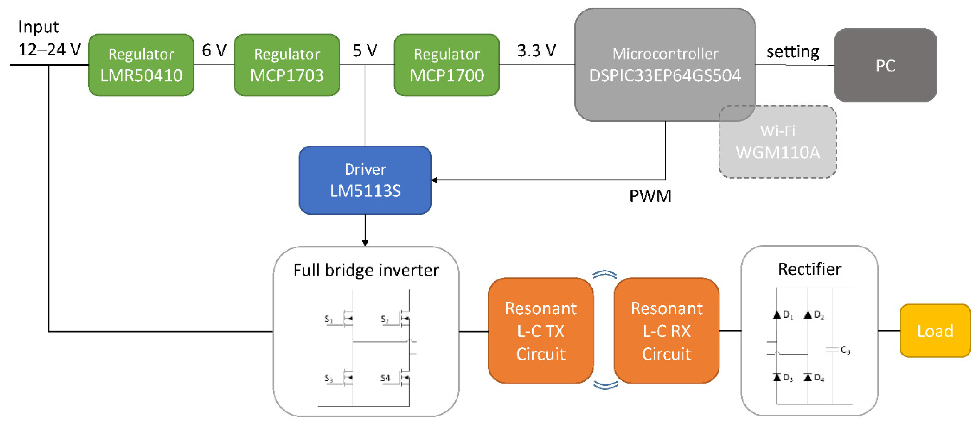
In order to control the power boards, a digital board was designed, which is easily connected to the former and is equipped with a dsPIC33EP64GS504 microcontroller [
45] responsible for generating the control signals for the switches. The board can also be equipped with an optional WGM110 Wi-Fi module [
46] through which it is possible to monitor the system, vary the converter parameters, and communicate the parameters and measurements to other devices. The power boards also include integrated circuits to regulate the input voltage (12–24 V) to the value required to supply the driver (5 V) and microcontroller (3.3 V).
The receiver circuit consists of a rectification bridge made with CDBA240LL diodes, a capacitance of 2.2 μF, and a variable resistive load.
To complete the system, two antennas (receive and transmit) were built with identical specifications, which constitute the LC resonant element of the circuit and have a design inductance of 1.05 μH. Each antenna is printed on a Printed Circuit Board (PCB) with a 35 μm thick copper layer and is constituted by a rectangular coil with two turns, with a track size and a space between tracks of 8 mm; the overall length and width of the coil are 184 and 128 mm, respectively. The resonant circuit is completed by inserting capacitances of an appropriate value in series to achieve the desired circuit resonant frequency. To achieve a resonance peak at 1 MHz, the two coils were tuned through capacitances of a nominal value of 22 nF. The equivalent parameters of the transmitting and receiving compensated circuits, measured with the network analyzer, are: LT = 1.10 μH, CT = 22.3 nF, RT = 0.61 Ω, LT = 1.07 μH, CT = 23.3 nF, RT = 0.63 Ω.
Figure 5 shows the block diagram of the overall system.
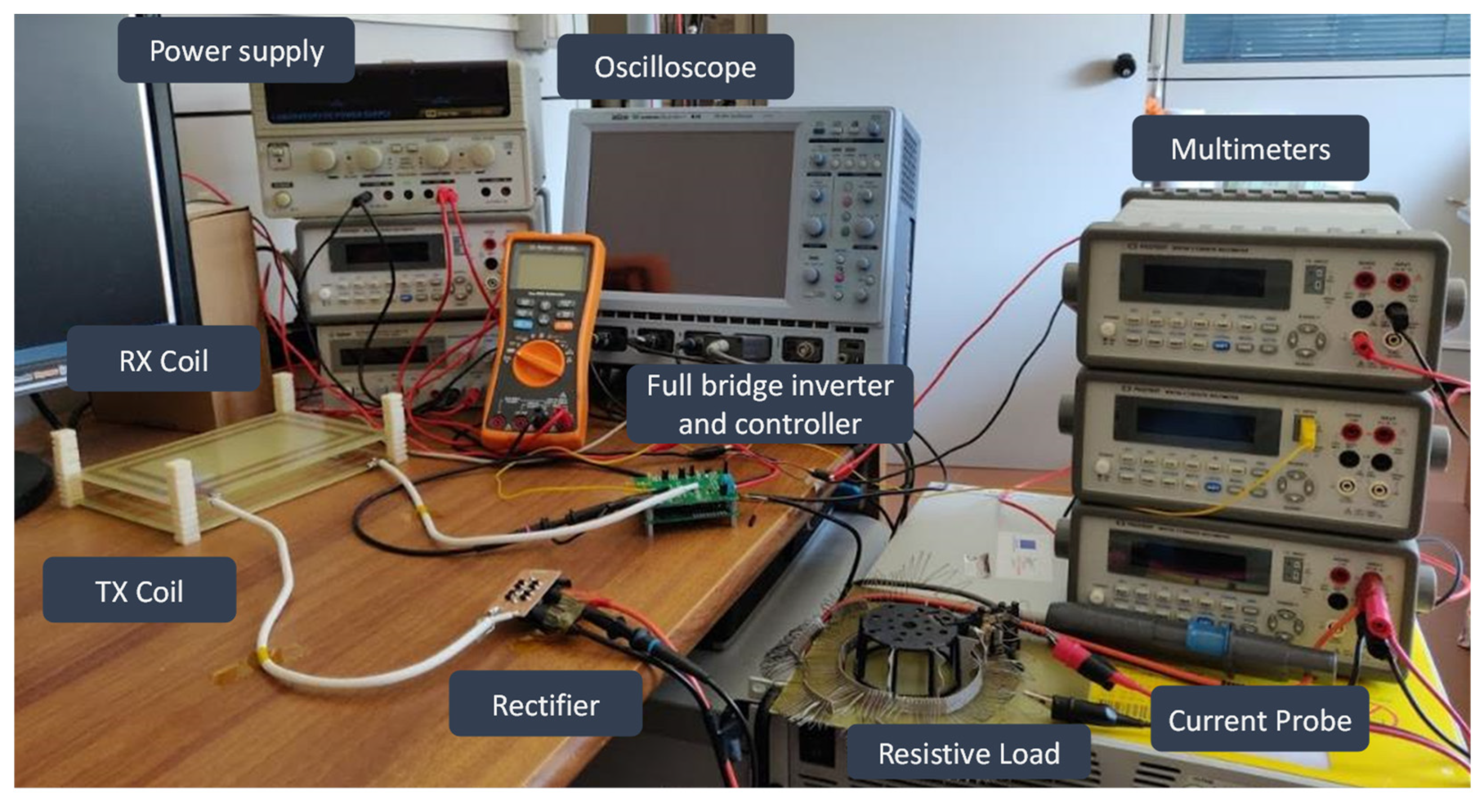
The measurement setup includes a Gw Instek GPS-3303 DC power source, which feeds the transmitter circuit, set to different voltage values according to the test requirements; and a 4-channel LeCroy Wavesurfer 434 oscilloscope, used to display the waveforms in the circuit and to measure the voltage on the load and current through the AP015 probe. Input voltages and currents are measured using Picotest M3510A multimeters. The power is calculated as the product of voltage and current; however, other more complex techniques for measuring power losses are possible [
47,
48,
49]. During the tests, the temperature was monitored through a type K thermocouple. The antenna coils, connected to the respective transmitter and receiver circuits, were placed at different distances employing 3D-printed spacers.
Figure 6 shows the whole measurement setup.
Figure 7 shows a flowchart of the workflow applied in this study.
3. Results
Numerous tests were performed on the boards, at different voltages, loads, frequencies, and power values, and at different distances between the transmitting and receiving coils. The measurements were intended to analyze and compare the general performance of the two WPT prototypes based on Si MOSFETs and GaN HEMTs.
The overall efficiency and the power transferred to the load were used as key performance parameters to evaluate the performance of the system. The efficiency is calculated as the total power at the load ratioed to the input power at the transmitter board and includes the consumption of all the elements of the circuit, such as the microcontroller, power supply, and the accessory circuits, whose overall consumption is between 0.45 and 0.51 W, varying according to the supply voltage of the system.
3.1. Silicon-Based Board Performance
At first, the silicon-based board was considered to evaluate the general performance of the WPT system and verify that its behavior is in agreement with what has been theoretically anticipated. The following charts show the performance of the system in different conditions. All the tests were performed with the resonant circuit set to resonate at 1 MHz, as outlined in the previous paragraphs. However, slight deviations in the coils’ resonant frequency are possible due to component tolerances and temperature variations.
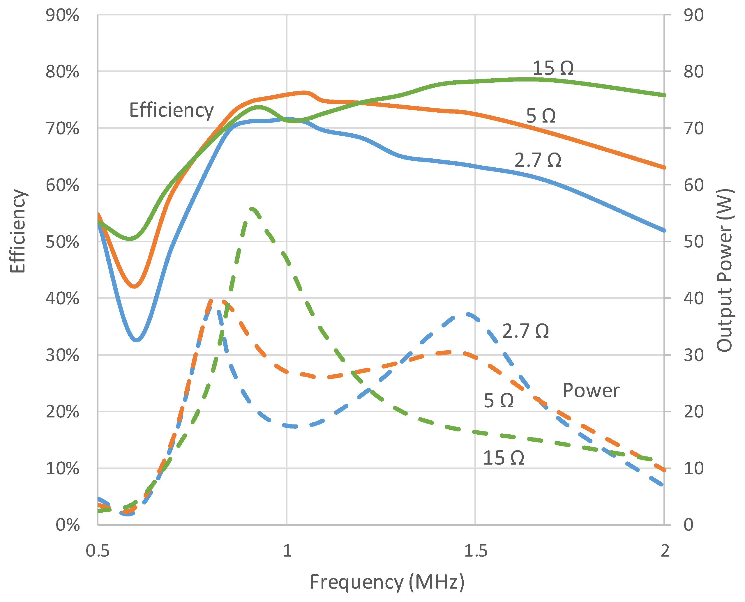
Figure 8 shows the efficiency and the output power of the WPT system by varying the inverter operative frequency, for three different load values (2.7, 5, and 15 Ω), with an input voltage of 15 V, at a fixed distance of 7 mm between the coils. The output power is not always the maximum at the resonant frequency but, at some loads and coupling conditions, it experiences a double-peak behavior as the frequency varies.
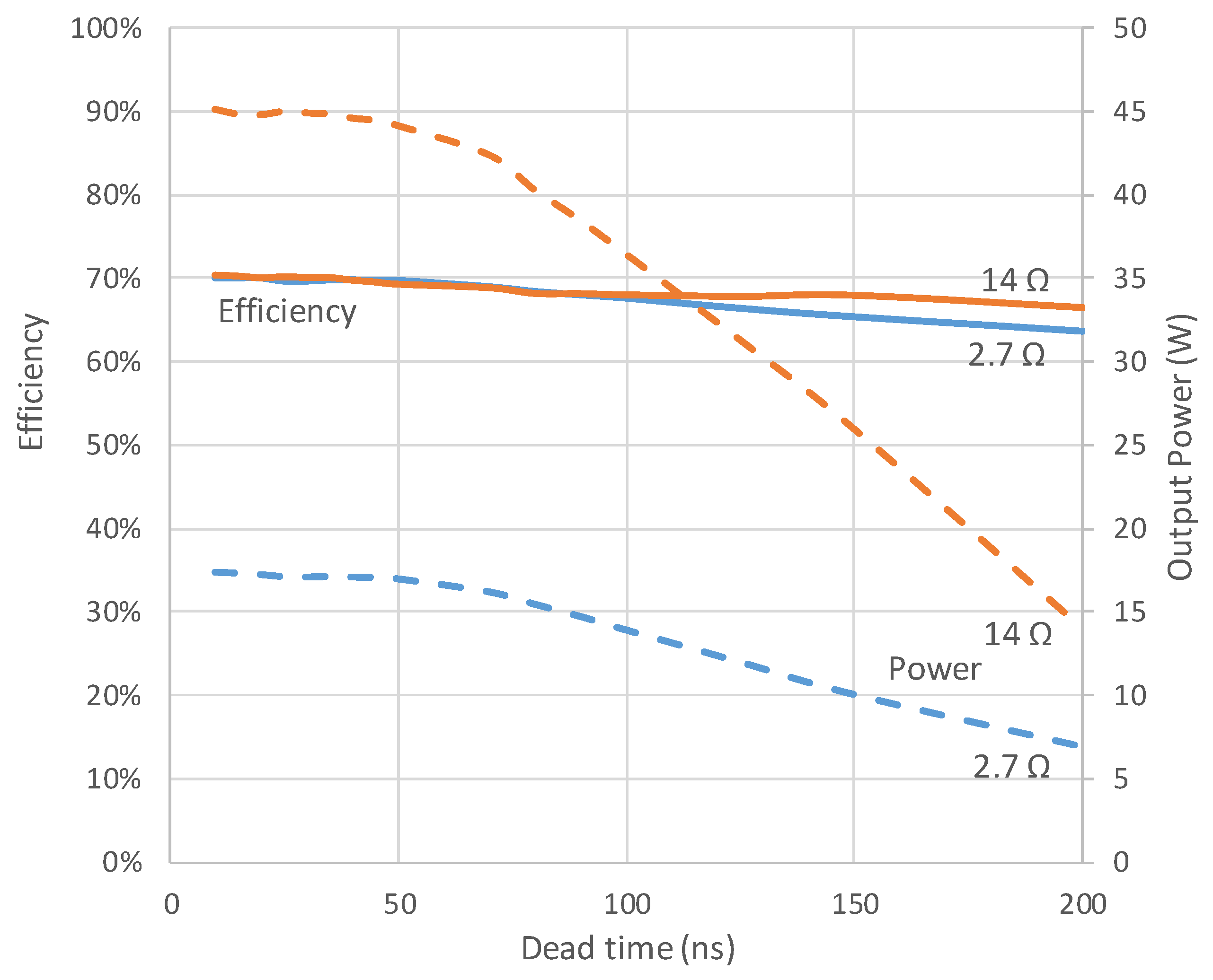
Figure 9 shows the performance by varying the dead-time of the MOSFET with two different loads (2.7 and 14 Ω) and an operative frequency of 1 MHz; the input voltage is 15 V and the distance between the coils is 7 mm. The dead-time value affects the efficiency and, even more, the power delivered to the load, which experiences a substantial decrease for increasing values of the dead-time. The manipulation of the dead-time and operating frequency can be used to tune the performances of the system and achieve the desired behavior.
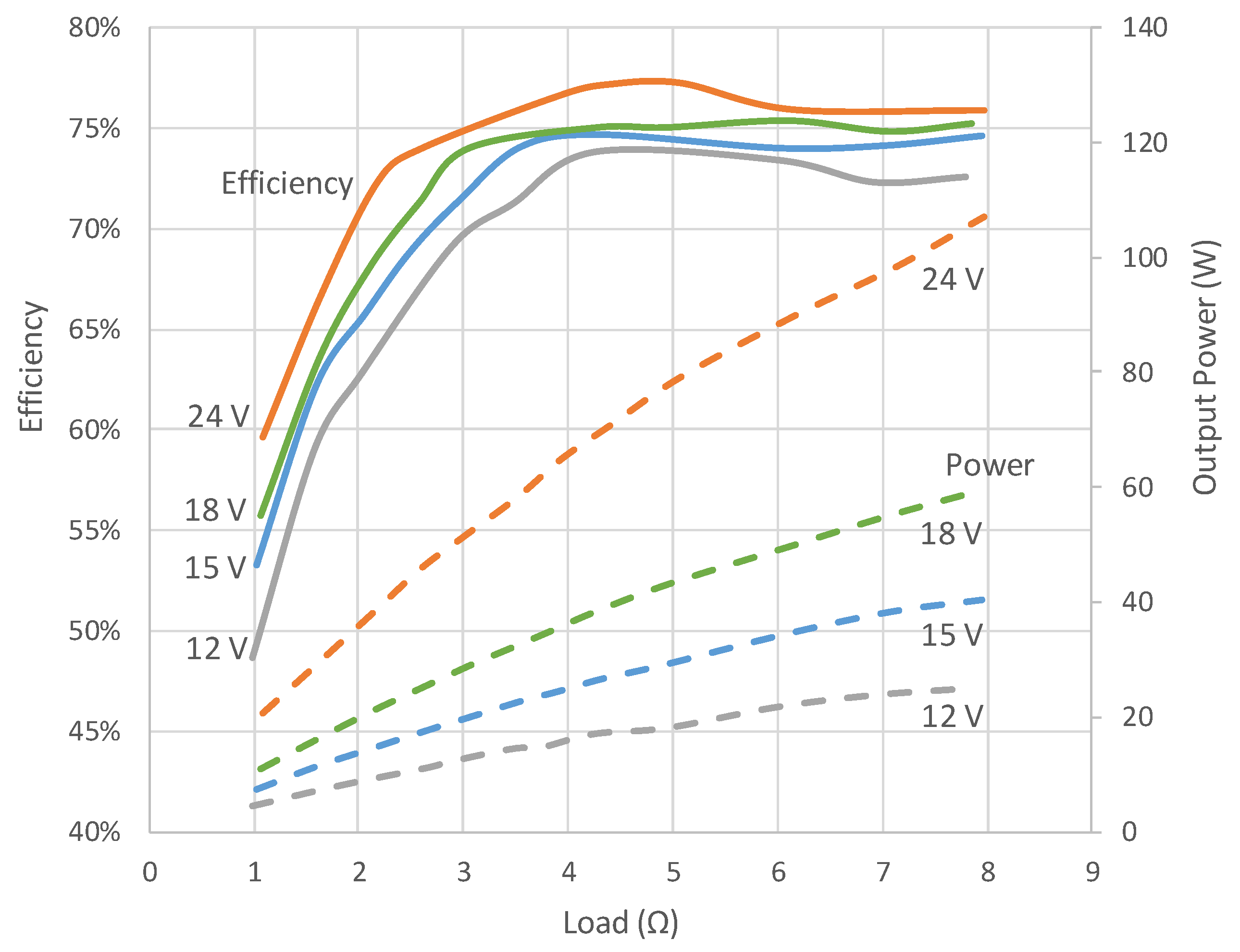
Figure 10 shows the system behavior of the WPT system at different input voltages (12, 15, 18, and 24 V), with a distance between antennas of 7 mm. The increase in input voltage clearly improves the system efficiency and allows higher output power to be to achieved. The calculation of the overall efficiency includes the losses in all the system components, such as the microcontroller, the DC regulators, and the accessory circuits, whose consumption is almost constant at different input voltages. Therefore, at higher input voltages, the power losses of these auxiliary components become less relevant and this, in fact, increases the overall efficiency. However, particular attention must be paid to the maximum voltage and current ratings of the components so as not to affect the system’s reliability.
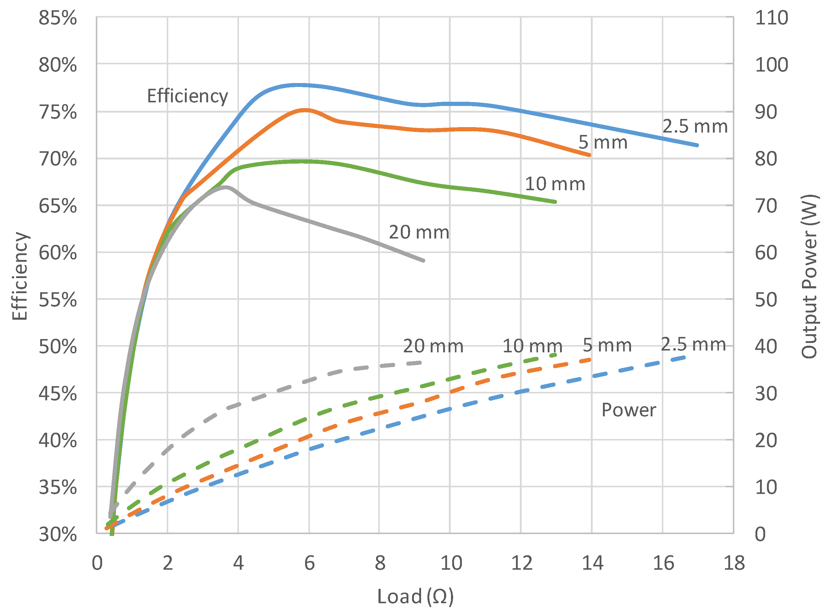
Figure 11 shows the system behavior by applying a 12 V input voltage at varying load values and for different coil distances (2.5, 5, 10, and 20 mm). By increasing the distance, the coupling coefficient is reduced and this involves a lower overall system efficiency. At higher coupling coefficients, the peak output power is achieved for high load values, as expected from the discussion relative to
Figure 3 in the previous section.
The system can transfer almost 40 W to the load with an efficiency of over 70% for an input DC voltage of 12 V. A large part of the lost power is due to power losses on coils’ equivalent resistances (see Equation (9)). When the board is supplied with 24 V input DC voltage, it enables the transfer of over 100 W to the load with an efficiency of almost 80%. Operating at a high coupling factor and high input voltage allows the maximum efficiency and output power to be achieved. At increasing distances between the receiving and transmitting antennas, the efficiency drops rapidly.
As expected for this resonant circuit topology, the power increases as the load increases in value and, for each distance, there is an optimal load that maximizes the power transfer efficiency. A DC-DC converter at the secondary could be used to track the maximum power point and transfer the maximum available power for every load and distance condition.
3.2. GaN-Based Board Performance
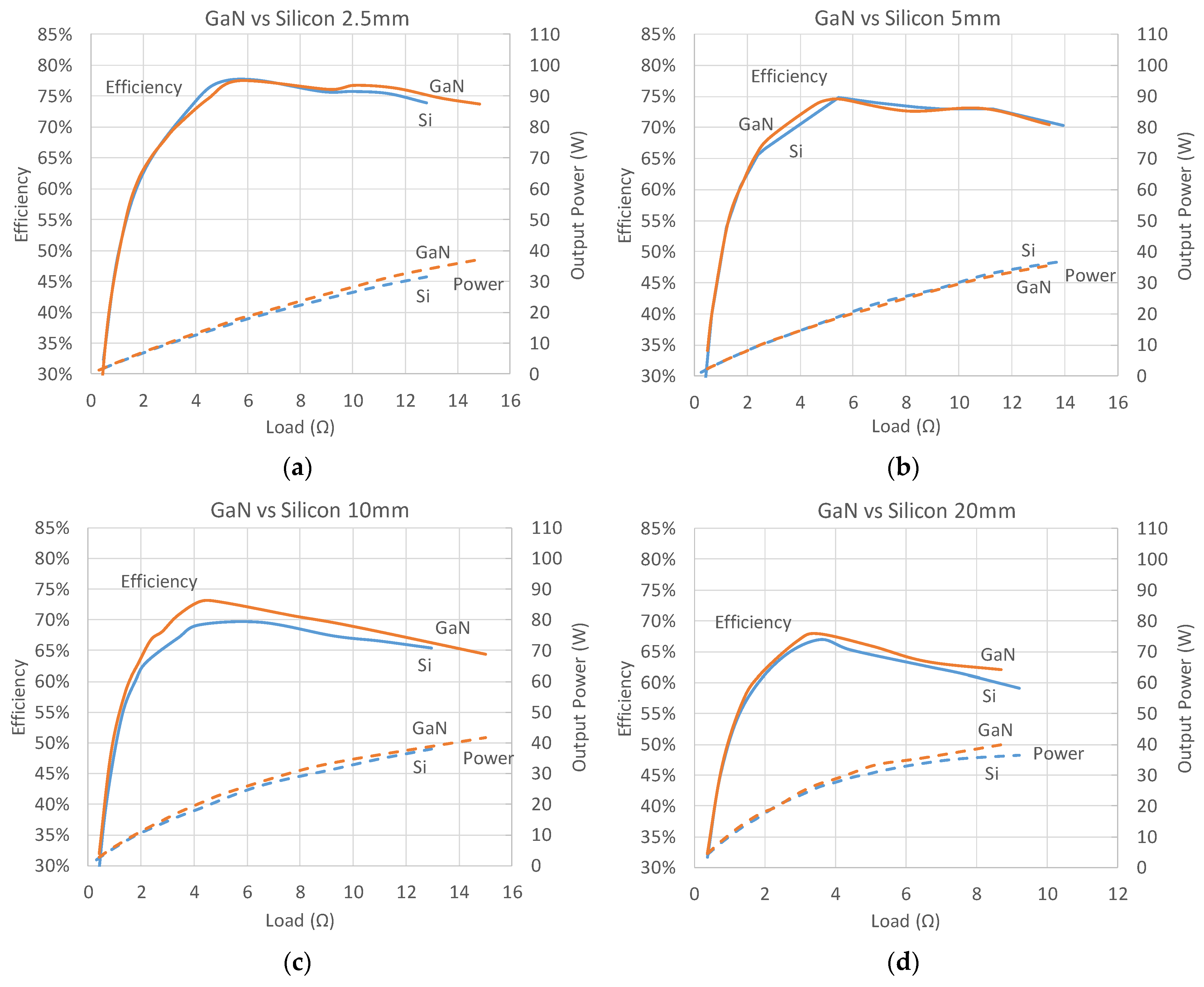
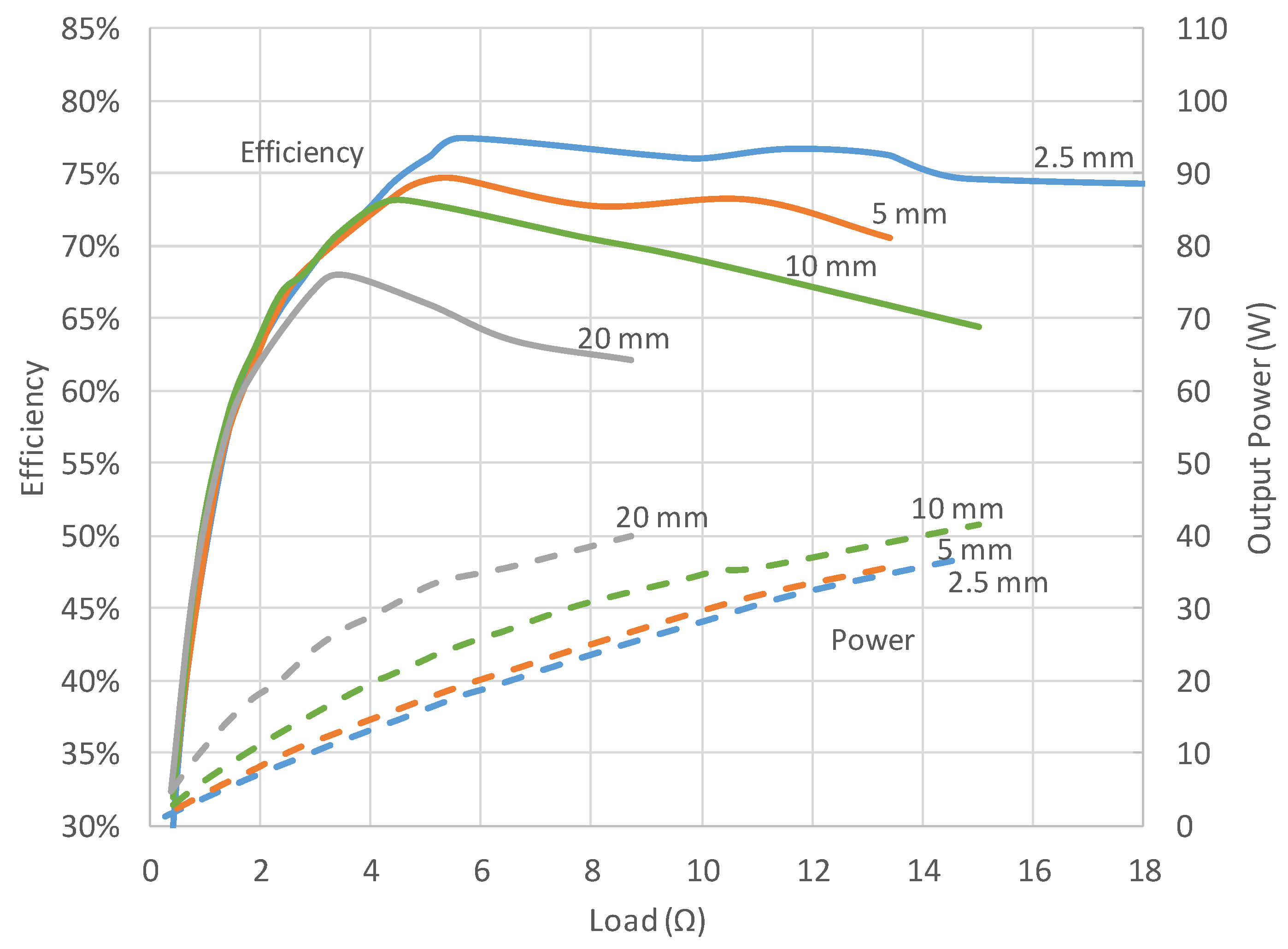
Figure 12 shows the performances of the GaN-based board at 12 V input voltage for different loads, at 1 MHz switching frequency, and at a distance of 2.5, 5, 10, and 20 mm, respectively.
When the two antennas are placed at a distance of 2.5 mm, the platform can transfer 40 W to the load with an efficiency of about 74% at an input DC voltage of 12 V. At increasing distances between the receiving and transmitting coils, the efficiency drops rapidly for the same output power value.
Figure 13 shows the comparison charts between the Si and GaN platforms for an operating frequency of 1 MHz, an input voltage of 12 V, and under different coil spacing operating conditions. The two platforms offer comparable system performance and power delivered to the load; however, the GaN-based board offers slightly better overall efficiency due to the better switching characteristics. When the spacing between the coils is narrow, the two boards provide a comparable peak efficiency value, whereas at higher distances the GaN system offers a slight percentage advantage of between 1% and 3.5%. Moreover, due to the lower internal resistance and better switching characteristics, the output power obtainable with the GaN devices at high load values is generally a few watts higher, up to 3.5 W at 8.7 Ω and 20 mm coil spacing. A major difference is expected when operating at higher resonance frequencies, where the very low turn-on and turn-off times of GaN devices can yield benefits by lowering the power losses in the inverter.
4. Discussion
The total system efficiency and the power transferred to the load are two key parameters to evaluate the performance of a WPT system. As it is not possible to optimize both parameters simultaneously, a designer can prioritize one of the two depending on the application; for example, the efficiency may be of crucial importance in a high-power system, whereas reaching a certain output power may have greater relevance for low-power applications.
Due to the power transfer behavior and the splitting phenomenon in relation to the operating frequency and system efficiency, the adoption of adaptive controls is recommended to maximize the transferred power; these controls may include impedance matching, frequency tuning, or the introduction of additional resonators.
The comparison between silicon and GaN systems shows that under the tested conditions, the GaN circuit generally performs better than the silicon one; nevertheless, a clear advantage of the GaN solution in every operating condition cannot be identified, despite its improved switching characteristics. The GaN-HEMT can, however, be the only viable option when operating at higher frequencies, for which the higher capacitance of the silicon MOSFET can compromise the performance of the entire system.
Table 1 summarizes the performance of the two WPT solutions and the cost of the switching devices, which are the only differences between the two WPT systems.
At the receiving circuit, the replacement of the traditional diode bridge with a GaN optimized synchronous rectifier can improve the overall system performance, but at the cost of increased complexity.
The overall efficiency of the system, however, depends on multiple factors, and the coupling between the transmitting and receiving coils is the factor that affects the overall efficiency the most. An accurate coil and resonant circuit design is of vital importance to achieve higher overall power transfer efficiencies.
5. Conclusions
The design, testing, and performance of two WPT circuits were presented in which the full-bridge feeding the resonant circuit is based on switching devices with different technologies, in particular GaN HEMTs and conventional Si MOSFETs. The aim of the study was to compare the performances of the two solutions and evaluate their impact on the overall WPT efficiency for systems operating at frequencies of the order of MHz.
Two custom-made hardware prototypes with identical circuit topology were designed and built, one with GaN and one with conventional Si switching devices, and several tests were carried out under different operating conditions, such as varying loads, frequencies, dead-time, supply voltages, and distance between the transmitting and receiving coils.
Experimental results on the two prototypes allowed us to directly compare the performances of the two circuits. The comparison shows that the GaN circuit typically performs better than the Si circuit, but a clear advantage of the GaN solution cannot be established under all the tested conditions. At small distances between coils, the two boards provide the same peak efficiency, whereas at larger distances the GaN-equipped board offers slightly higher efficiency in the order of 1–3%. The GaN solution also provides higher maximum output power, up to 10% higher in the tested range.
The overall efficiency of a WPT system depends on multiple factors and the efficiency of the full-bridge’s switching devices is just one of them. The higher costs of GaN HEMT devices compared to traditional silicon FETs may not justify their use at switching frequencies up to a few mega-Hertz. However, the GaN devices can represent an advantage when operating at higher frequencies, due to the better dynamic performance compared to Si devices.


 ,
, 


