Abstract
This article introduces a three-phase capacitor clamped inverter with inherent boost capability by relocating the filter components from the AC side to the configuration’s midpoint. This topology has several distinguishing characteristics, including: (a) low component count; (b) high DC-AC gain; (c) decreased capacitor voltage stresses; (d) improved power quality (extremely low voltage and current THDs) without the use of an AC-side filter; and (e) decreased voltage stresses on power semiconductor devices. Simulations were carried out on the MATLAB Simulink platform, and results under steady-state conditions, load and reference change conditions, and phase sequence change conditions, along with THD profiles, are presented. This inverter’s performance was compared to that of similar converters with intrinsic gain. A 1200 W experimental prototype was built to demonstrate the system’s feasibility and benefits. When compared to existing topologies, simulation and experimental results indicate that the proposed inverter provides superior high gain, smooth control, low stress, and a long life time.
1. Introduction
To overcome the disadvantages of the traditional inverters, such as voltage sources and current source inverters, the ZSI/qZSI [1,2] is widely accepted for various applications. The ZSI/qZSI offers a voltage step-up/down function in single-stage power conversion without requiring additional power processing stage, as shown in Figure 1a, and its application in an electric vehicle is depicted in Figure 1b. Moreover, ZSI/qZSI’s reliability is high because shoot-through is an integral part of the operation. The study of these converters has mainly focused on control techniques [3,4,5], applications [6], and PWM schemes [7,8].
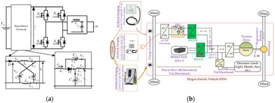
Figure 1.
(a) Classical impedance source converters and (b) their applications in EV.
In addition, various power electronics topologies have been proposed in the literature to meet the different objectives, such as reducing the number of switches, reducing the passive component count, and increasing the voltage gain and voltage stresses on the switches/capacitors. The SBI [9] is one such topology that was introduced to decrease the number of passive components (one inductor and one capacitor) in comparison to the ZSI/qZSI by having one additional switch. Although the SBI can perform voltage step-up or step-down in a single stage, its voltage gain is significantly less than that of impedance source converters such as the ZSI/qZSI (1-D). To enhance the source current profile and voltage gain, a group of qSBIs was reported in [10,11]. These included dc-link and embedded-type qSBIs, in addition to current-fed SBIs. However, the embedded-type qZSI necessitates the use of two distinct DC sources, which is undesirable. The qSBI has similar characteristics to the qZSI, except that the shoot-through mode is used for voltage boosting. A comprehensive comparison of the qSBI and qZSI was described [12]. However, the shoot-through duty cycle in these topologies cannot exceed (1–M), where M is the modulation index, thereby limiting the voltage gain in all of the above-mentioned topologies. To achieve the desired output voltage with a high voltage gain and good power quality, a high-duty cycle must be used, lowering M. The lower the value of M, the lower the overall DC-AC conversion gain and the higher the output harmonics. Either the M or the B.F. can be increased to increase the overall DC-AC gain. Numerous PWM techniques have been proposed for modifying the modulating waves, and it has been demonstrated that PWM schemes can only slightly increase M [7]. Numerous high-gain inverter circuits with and without a galvanic isolation transformer have been proposed [13,14,15,16,17,18,19,20,21,22,23,24,25] to increase the boost factor in impedance source converters. Transformer-based ZSIs have been introduced [13,14]. However, the transformer’s leakage inductance results in voltage spikes at the DC-bus. To achieve a high voltage gain, transformerless ZSIs with additional passive components, such as inductors, capacitors, and diodes, have been proposed [15,16,17,18,19,20,21,22,23,24,25]. They have been labelled L-ZSI [15], SL-ZSI [16], SL-qZSI [17], EB-ZSI [18], DA-qZSI [19], CA-qZS [20], and EB-qZSI [21], and by incorporating switched-inductor, switched-capacitor, and hybrid switched-capacitor/switched-inductor designs, high boosting factors can be achieved. The addition of passive elements and power electronic components, on contrast, increases the converter’s cost, size, volume, losses, and weight [24,25].
For single-phase and three-phase applications, the aforementioned topologies have been proposed. A simple single-phase HB ZSI with reduced capacitor voltage stress was described in [26]. Although this topology is straightforward and compact, it has a low boost factor. In [27], an HB-SBI with discontinuous input current was introduced to increase the gain of the inverter. To address the shortcomings of the HB-SBI, [28] proposed the HB-qSBI. The overall voltage gain is low in all of these half-bridge topologies [26,27,28]. By comparison, in the SL-ZSI [16], SL-qZSI [17], EB-ZSI [18], DA-qZSI [19], CA-qZSI [20], and EB-qZSI [21] topologies, the voltage stresses on the capacitors are greater, and these topologies employ a greater number of capacitors. The capacitor voltage is typically greater than the input voltage in order to perform the impedance-source stage’s voltage boost function. As a result, high-voltage Z capacitors must be used, potentially adding volume and cost to the system. Because of the strong probability of capacitor failure during the field operation of power electronic converters [29], and the stringent reliability restrictions imposed by the aerospace, automotive, defense, space, and energy industries, stresses and use of capacitors must be reduced to improve inverter reliability [30].
Overall, all of the mentioned topologies have common issues, such as the requirement for capacitors having a high voltage rating (greater than supply), common mode voltages, PWM-natured voltages after the inverter switching leg, and a higher component count when achieving a boosted DC-AC gain in a single stage manner. To address these issues, the capacitor clamped boost inverter with high voltage gain was introduced [31], which disperses the X-shaped passive components of the impedance source inverter rather than concentrating them in one location (between the input and inverter switching network in impedance source inverters). The passive components are distributed evenly between the input and output ports on each leg. However, ref. [31] does not deal with detailed steady-state analysis. Hence, in this study, a detailed analysis in various modes based on the inductor current iL bands (upper (iLmax) and lower bands (iLmin)) was conducted. Based on the upper and lower band values, the operation was divided into three zones in this study. Based on the aforementioned zones, the operation of the converter was further divided into two cases: case-I (zone-1 and zone-3) and case-II (zone-2). In addition, this manuscript includes capacitor voltage profiles and capacitor life time calculations. This paper also discusses the design of a sliding mode controller for the CCBI to track the required voltages and currents to fulfil the specified load characteristics. Also shown are the CCBI’s performance under load, reference, and phase sequence change conditions, and its THD profiles. In addition, the performance of this inverter for non-linear loads was also examined. The operating principles, steady-state analysis of various cases, differential modulation technique, capacitor voltage profiles, capacitor life time calculations, and sliding mode controller for the CCBI are presented in Section II. Simulation results and a discussion of the results under steady-state conditions, load and reference change, and phase sequence change conditions, along with THD profiles, are discussed in Section III. A performance investigation of this inverter for non-linear loads is also presented. In the same section, comparative analysis of the proposed inverter with existing similar converters is also presented, along with experimental verification. Section IV presents the conclusions.
2. Operation of the CCBI
The proposed inverter, depicted in Figure 2a, includes six switches, three small inductors, and three capacitors. Because of the time-varying duty cycle, the intrinsic boost feature of this proposed inverter provides flexibility for grid-connected and stand-alone applications, for a large range of AC output voltages, which are even higher than the DC voltage. This capability is not accessible in standard VSIs, where the DC input voltage is always greater than the AC output voltage [11]. The following offers an analysis of the converter in various modes, a differential modulation scheme, capacitor voltage profiles, a life time analysis, and a sliding mode controller.
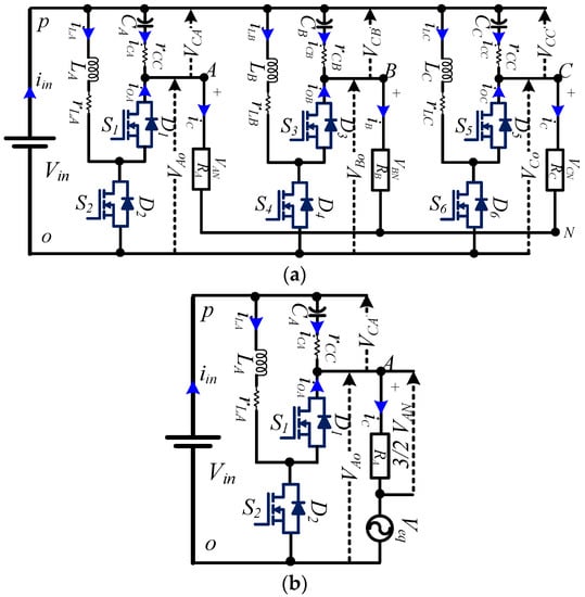
Figure 2.
(a) Proposed converter; (b) single-phase equivalent circuit.
2.1. Analysis of Converter
The operation of the converter shown in Figure 2a is explained with the help of a single-phase equivalent circuit, which is shown in Figure 2b. The equivalent circuit contains one leg (phase-A) along with considerations of the effect of other phases. Boost inverter upper switches are represented with odd numbers, whereas lower switches are represented with even numbers, and these switches operate in a complementary manner. Every inverter leg contains one inductor, one capacitor, and two switches. Analysis of the boost inverter is explained via mathematical modeling.
For one cycle (0 < t < T) of load current (iLoad), the average value of the inductor current (iL) is positive and negative for the periods (0 < t < T/2) and (T/2 < t < T) respectively, which is shown in Figure 3, where T = 1/f. It can be observed that iL is oscillating at the switching frequency of fs between two bands, namely, the upper band (iLmax) and the lower band (iLmin). During the positive half cycle, the upper band is always positive. However, the lower band current value is negative in zone-1 (0 < t < Ta) and zone-3 (T/2 − Ta < t < T/2), whereas it is positive in zone-2 (Ta < t < T/2 − Ta). Here, Ta is the time when zone-1 comes to an end.
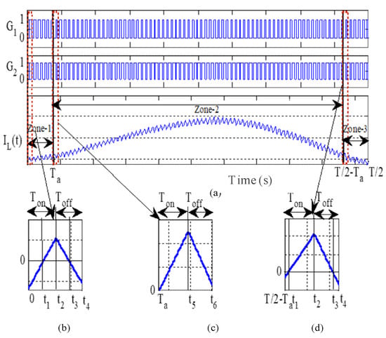
Figure 3.
(a) Gate signals of S1 and S2 and inductor current for positive half cycle; inductor current in one switching cycle of (b) zone-1, (c) zone-2, and (d) zone-3.
Based on the aforementioned zones, the operation of converter is divided into two cases, case-I (zone-1 and zone-3) and case-II (zone-2) as shown in Figure 3. To simplify the analysis further, only one switching sample is considered of N (=fs/f) samples, and the detailed description of both cases is given below.
case-I (zone-1 and zone-3): It is interesting to note that, in this case, all the semiconductor devices sequentially (D2, S2, D1, and S1) participate in one switching sample of G2, which is shown in Figure 4. Based on the conduction of these switching devices, the operation of the circuit in this case is further classified into four modes, and its equivalent circuit in each mode is shown in Figure 4. The operation of the inverter in various modes for case-I is explained below.
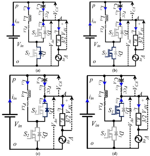
Figure 4.
Equivalent circuit in various modes: (a) Mode-1; (b) Mode-2; (c) Mode-3; (d) Mode-4;
Mode-1 (0 < t < t1): This mode starts when the gate signal is applied to the lower switch S2. However, S2 cannot be turned on instantly due to the fact that the inductor does not allow the sudden change in current, as it is has a negative value in the previous mode. This leads the diode D1 to be turned on and provide a path for a negative inductor current, as shown in Figure 4a.
This iL increases linearly in the presence of a positive supply voltage, as shown in Figure 5, and its current equation can be written as:
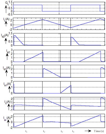
Figure 5.
Waveforms during case-I.
This mode ends at , where iL becomes zero and diode D2 turns off. The time duration of this Mode-1 can be calculated as:
Mode-2 (t1 < t < t2): This mode starts at t = t1 when S2 comes into conduction. In the presence of a positive supply voltage (Vin) across the inductor, its current is increases linearly from 0 to ILmax, as shown in Figure 6, and its equation can be written as:
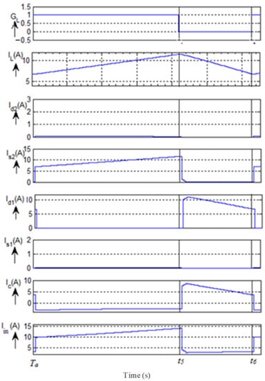
Figure 6.
Waveforms during case-II.
This mode ends at , when the switching pulse for S2 is removed and the time duration of this mode can be evaluated as:
Mode-3 (Ton < t < t3): This mode starts when the gate signal is given to switch S1. From the previous state, it is clear that the initial inductor current is positive (ILmax), which brings diode D1 to conduction, even in the presence of firing pulses at G1, as shown in Figure 6. During this period, a negative voltage (Vin − VAO) appears across the inductor, which leads to the decrement of the inductor current with a negative slope of (Vin − VAO)/L, which can be expressed as:
This mode ends at t = t3, when reaches zero and forces the diode to be turned off. The duration of this mode can be determined as:
Mode-4 (t3 < t < T): The zero-initial current of the inductor and the presence of the switching pulse brings S1 to conduction mode. Now, the inductor discharges in the presence of a negative voltage (Vin − VAO) and, hence, the inductor current is decreased to a specific negative value (ILmin). This negative inductor current is the initial current for Mode-1. The expression for the inductor current is given as:
This mode ends with the removal of the gate pulse of S1 and the duration of this mode can be calculated as
The same cycle of operation repeats until t = Ta. The inductor voltage balance equation during case-I can be written as:
where is the duty cycle at the ‘kth’ switching sample of switch S2 of phase A. Waveforms during this case shown in Figure 5. As dA is a time-varying value, and when d > da at t = Ta, case-I ends.
case-II (Ta < t < T/2 − Ta): This is the special case where Mode-2 and Mode-3 operations of case-I only take place as there is no negative value of iLmin and the remaining two cases are absent. In this case, only two semiconductor switches take active participation in conversion, namely, S2 and D1, whereas the remaining two are in an idle state. Hence, two modes are sufficient to explain the operation; waveforms during this case are shown in Figure 6. It can be observed from the characteristics presented in Figure 5 and Figure 6 that case-II is a special case of case-I, where only two modes (Mode-2 and Mode-3) are presented during operation. Waveforms of lower switch gate pulses, inductor current, upper and lower diode and switch currents, coupled capacitor current, and input current are presented in Figure 6 respectively. A detailed explanation is presented below.
Mode-1(Ta < t < t5): This mode starts at t = Ta, at which instant firing pulses (G2) are given to S2. Due to a positive initial inductor current and the presence of G2, switch S2 is turned on. In the presence of a positive voltage across the inductor, it is charged to a specific value, which can be expressed as:
This mode ends at t = t5 when firing pulses are removed from G2.
Mode-1 (t5 < t < t6): This mode of operation starts when pulses are given to S1. Although pulses are presented at S1, it cannot be turned on due to the positive initial current in the inductor. This turns on diode D1. Now, the negative voltage across the inductor causes a decrement in the current with the negative slope of , which can be expressed as:
This mode ends at t = t6 when firing pulses are removed from S1. A similar operation (Mode-1 and Mode-2) continues for several switching cycles until (T/2 − Ta). The voltage balance equation of the inductor obeys Equation (8), as discussed in case-I. Furthermore, the similarly boosted inverter operates in a negative half cycle, with the major role of S1, D2 in T/2 to (T/2 + Ta), and (T − Ta) to T, in addition to D1, S1, D2, and S2 during (T/2 + Ta) to (T − Ta).
2.2. Differential Modulation Technique for Three-Phase Boost Inverter
As shown in (8), once the duty cycle becomes zero, VAO = Vin; this shows that this converter outputs a dc bias voltage in relation to the negative supply terminal. The primary goal of this study was to generate three-phase sinusoidal voltages across the load terminals of Figure 2a. Based on the gain of this boost inverter, we assume these voltages are modulated with the following duty cycles (dA, dB, and dC) as follows [13]:
where dA, dB, and dC are the duty cycles of the A, B, and C phases, respectively, Vin is the bias DC voltage of the boost inverter (i.e., supply voltage), and A is the sinusoidal voltage amplitude. It should be noted that the CCBI one-leg voltage with regard to the negative terminal of a source (VAO, VBO, VCO) always has the same sign as Vin; thus, (VAO)DC must be added to maintain this necessary condition:
Here
From the equivalent model of the boost inverter, as shown in Figure 2b, the phase voltage applied to of the system can be obtained as [2]:
The first term in (14) is the voltage VAO produced by the same phase of the boost converter, whereas the second and third terms account for the influence of the other two phases. It can be understood that the phase voltage of the load is a function of all of the three phases’ leg voltages (VAO, VBO, and VCO), and for the particular load phase voltage, the other phases’ leg voltages’ combined effort can be grouped as:
The difference in VANVeq should also cause the same phase current in the model, so an equivalent resistance can be introduced, as mentioned below:
From Equations (12) and (14):
In a similar way, VBN and VCN have a 120° phase shift at the load terminals. Therefore, the phase-to-neutral voltages at the load are:
These ideal outcomes can be achieved by calculating the three-phase duty cycles using:
2.3. Capacitor Voltage Profile
One of the main objectives of this study was to reduce the capacitor peak voltages, which can be calculated for the CCBI as follows:
Here
, and can be calculated as:
Whereas in case of other topologies, the capacitor voltages are higher due to the requirement of a higher dc link voltage for the required DC-AC conversion. Capacitor voltage profiles for the DC-AC conversion of 1 to 1.8 in the proposed case and other similar impedance source inverters are shown in Figure 7, which depicts the reduction in voltage stress on the capacitor.
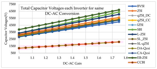
Figure 7.
Capacitor voltage profiles.
2.4. Life Time Calculation for Capacitor
To examine the life time benchmarks of different capacitor solutions and online condition monitoring, life models are used. Generally, the life time of the capacitors is greatly influenced by two factors, namely, voltage stress and temperature. The most extensively accepted empirical model for capacitor life is:
where is the life time under use conditions, is the life time under test conditions, V is the voltage at use conditions, and V0 is the voltage at test conditions. and are the temperature (Kelvin) at use and test conditions, respectively. Ea is the activation energy, KB is Boltzmann’s constant (8.62 × 10⁻⁵ eV/K), and n is the voltage stress exponent.
From (22), it is clear that Ea and n are the key parameters to determine the life time; its values were found to be 1.19 and 2.46 for high dielectric constant ceramic, and 1.3–1.5 and 1.5–7 for MLC-Caps.
For Al-Caps and film capacitors, a simplified model from (22) is popularly applied as follows [14]:
2.5. Sliding Mode Controller
When a sliding mode controller is adopted, the system performs effectively in both steady-state and dynamic operations. Although more complicated control approaches, such as THD, can increase system performance, the observed results look satisfactory in many circumstances of practical importance, while the basic controller lowers system cost. An experimental prototype was created, and the experimental findings show that the converter is capable of step-up [2].
The following reasonable assumptions must be considered when designing the sliding mode controller for the proposed converter: power switches that are ideal, converters that operate at high switching frequencies, and power supplies that are free of sinusoidal ripple. Each phase of the proposed converter has two state variables. The sliding surface equation of state space in a three-phase system is expressed as:
where:
In sliding mode control theory, sensing of all state variables is required to generate the proper control signals and obtain the required AC supply. The generation of the inductor current reference is difficult to assess because it is dependent on several factors, such as supply voltage, load demand, and load voltage. As a result, iL-iLref can be generated directly from the high frequency component of the inductor current feedback signal, which must be removed due to the control strategy by designing a suitable high pass filter. The addition of a high pass filter increases system order and has the potential to change system dynamics. To overcome this issue, the selected values of the CCBI’s switching frequency were higher than the filter cut-off frequency. The trajectory of the sliding surface for this design is shown in Figure 8.
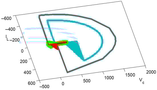
Figure 8.
Trajectory of the sliding surface.
3. Results and Discussions
The proposed CCBI, as shown in Figure 9, was successfully assessed by means of both simulations and prototype-based hardware results. Simulations were carried out using the MATLAB Simulink environment, and the parameters considered for the simulations are summarized in Table 1, as shown below.
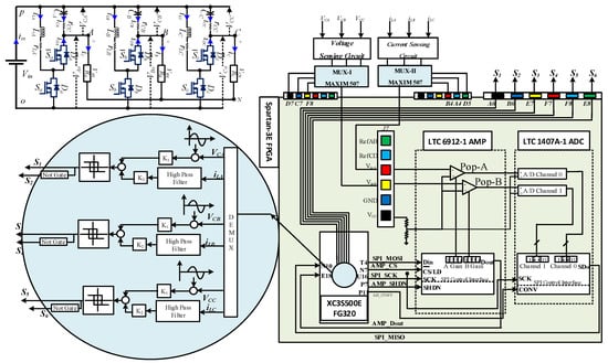
Figure 9.
Complete system diagram of the hardware setup.

Table 1.
Electrical parameters of the system.
The following results were acquired at the average switching frequency (Fs) equal to 10 kHz. A sliding mode controller was used to achieve good dynamic response, high robustness, and noise-free response while tracking the required AC from DC supply. System state variables were continuously monitored and controlled near to a zero error response with the hysteresis band = 0.3, filter constant = 0.01, K1 = 0.304, and K2 = 0.2. System performance was evaluated in both a steady state and transient states while feeding power to different types of loads (linear and nonlinear) under different test conditions. Phase voltages, line voltages, and load currents obtained from this inverter are shown in Figure 10, Figure 11 and Figure 12, respectively. From these results, it can be clearly seen that the input low-level DC supply was successfully converted to ideal sinusoidal three-phase AC power.
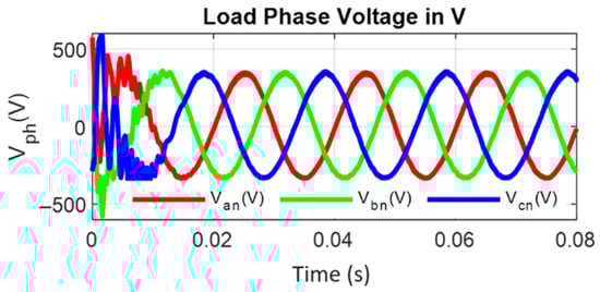
Figure 10.
Phase voltage of the inverter during steady-state conditions.
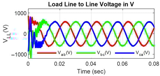
Figure 11.
Line voltages of the inverter during steady-state conditions.
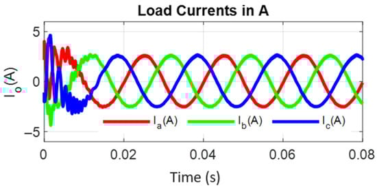
Figure 12.
Load currents of the inverter during steady-state conditions.
In the boost inverter topology, at least one capacitor is placed in every leg of the respective phase of the converter for the boosting operation. The negative terminals of each of the three capacitors of the three-phase inverter are connected to a common point in this topology, and these are also shown in Figure 13. With reference to this point, the common mode capacitor voltage (CMMCV) is defined as the average of all of the three capacitor voltages (VAO, VBO, and VCO) and is shown in Figure 14. In Figure 14, the conventional CMMCV is calculated for the topology proposed by Cecati and compared with the proposed topology. Figure 14 shows that the CMMCV across all of the three capacitors is greatly reduced by the proposed scheme, due to the fact that the individual capacitor voltage is also lower than that of the conventional topology. Figure 15 and Figure 16 were captured for the critical evaluation of the harmonic content contained at the output. These results show the THD waveforms of phase voltage, line voltage, and load current, respectively; from these results, it can be clearly understood that this inverter offers good quality of AC output without any lowest order harmonics (<3% of fundamental) for resistive load. All of the harmonic quantities are lower than 1.5% of the fundamental.
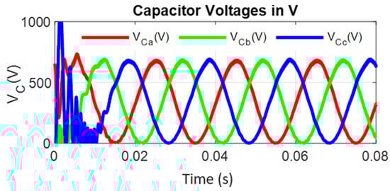
Figure 13.
Capacitor voltages of the inverter during steady-state conditions.
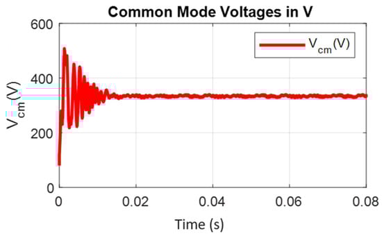
Figure 14.
Common mode capacitor voltages.

Figure 15.
THD waveform of line voltage.
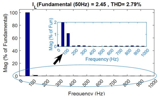
Figure 16.
THD waveform of load current.
In order to assess the dynamic performance of the converter, sudden changes were incorporated during the operation of the converter at load (increased by 50% and decreased by 50%), and in the reference voltage (decreased by 50% and changed the phase by 180°), and results were captured in each case for analysis. Figure 17 shows the current drawn by the 100% load (1.2 kW) from (0 to 0.04 s) and 50% load (0.6 kW) from (0.04 to 0.08 s), whereas Figure 18 depicts the opposite case of loading, i.e., 50% loading from (0 to 0.04 s) and 100% load from (0.04 to 0.08 s). Figure 19 was captured when the mode of operation is suddenly changed from active mode to regeneration mode at 0.04 s. Although the mode is changed from the active mode to the regeneration mode, the voltage amplitude remains constant, and its harmonics also remain the same. Figure 20, Figure 21, Figure 22 and Figure 23 show the phase voltages, line voltages, load currents, and capacitor voltages observed when the reference voltage is suddenly changed from 100% to 50% at 0.04 s. Whenever the reference voltage is changed, the output voltage changes, and the current also changes accordingly for the resistive load. THD waveforms in the case in which the reference voltage is changed were captured after the disturbance was settled, and are shown in Figure 23, Figure 24 and Figure 25. These results (Figure 20, Figure 21, Figure 22 and Figure 23) reveal that the CCBI with a sliding mode offers good dynamic response in stable operation, even for all kinds of disturbances, as discussed earlier.
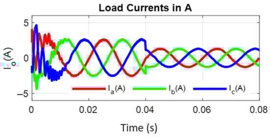
Figure 17.
Load current for a linear load with a step change in the load from 100 to 50%.
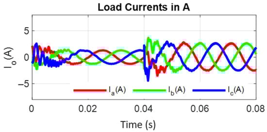
Figure 18.
Load current for a linear load and a step change in the load from 100 to 50%.
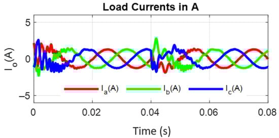
Figure 19.
Load current for the inversion mode of the load.
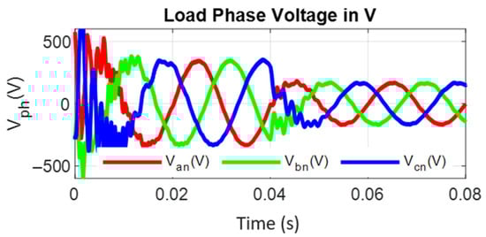
Figure 20.
Phase voltages for a linear load and a step change in the reference load voltage from 100 to 50%.
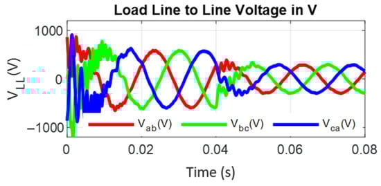
Figure 21.
Line voltages for a linear load and a step change in the reference load voltage from 100 to 50%.
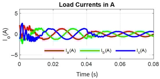
Figure 22.
Load currents for a linear load and a step change in the reference load voltage from 100 to 50%.
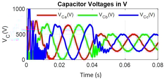
Figure 23.
Capacitor voltages for a linear load and a step change in the reference load voltage from 100 to 50%.
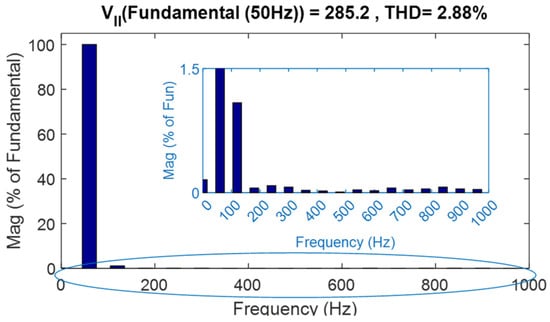
Figure 24.
Load voltage and load current for a linear load and a step change in the reference load voltage from 50%.
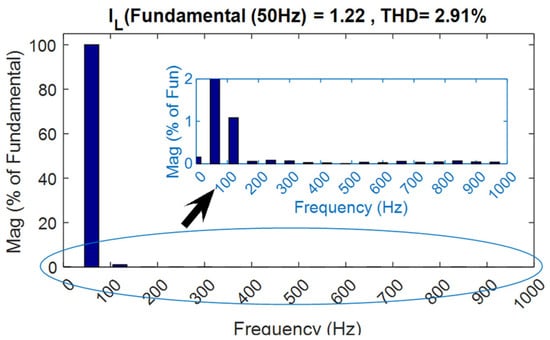
Figure 25.
Load voltage and load current for a linear load and a step change in the reference load voltage from 100 to 33%.
For critical evaluation of the converter, the inverter output is fed to a nonlinear load (three-phase diode bridge rectifier with R Load of 255 Ω), and Figure 26, Figure 27, Figure 28, Figure 29, Figure 30, Figure 31, Figure 32 and Figure 33 show the CCB inverter-fed diode bridge output currents and voltage, the diode bridge input line voltage and currents, the capacitor voltages of CCB and CMMCV, and the harmonic spectra of diode bridge input voltage and currents, respectively. Under steady-state mode, the diode bridge rectifier-fed resistive load absorbs the highly distorted current of 31.39% THD and voltage of 7.25% THD, as shown in Figure 32 and Figure 33, respectively. All of the foregoing data show that the CCB inverter has good behavior, and particularly superior dynamic behavior, which is mostly due to the lower values of the boost capacitances and voltage across the capacitor. This performance is especially notable when compared to that of a current source inverter (CSI); whereas the proposed system employs three independent small inductors, the CSI employs only one large inductor, resulting in much poorer dynamic performance.
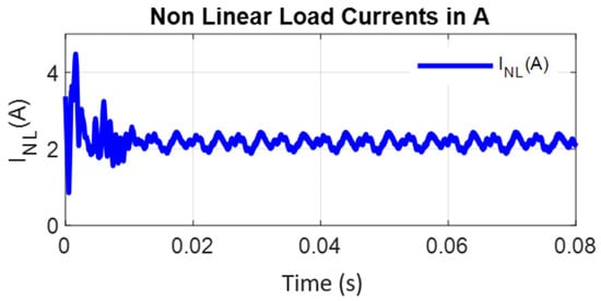
Figure 26.
Non-linear load (diode bridge) output currents.
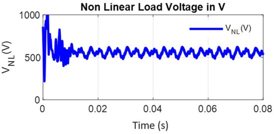
Figure 27.
Non-linear load (diode bridge) output voltages.
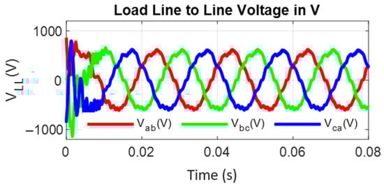
Figure 28.
Non-linear load (diode bridge) input voltages.
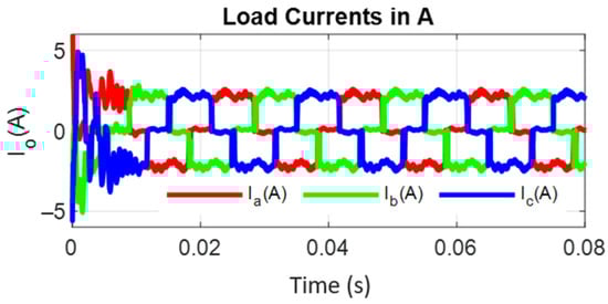
Figure 29.
Non-linear load (diode bridge) input currents.
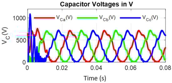
Figure 30.
Capacitor voltages of the CCBI.
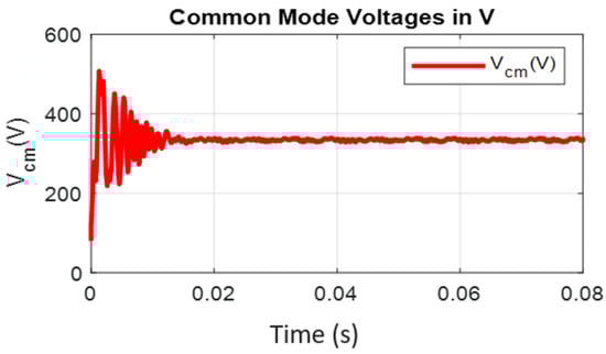
Figure 31.
Common mode voltages of the CCBI.
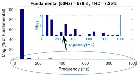
Figure 32.
CCBI voltage THD for the nonlinear (diode bridge) load.
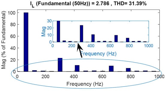
Figure 33.
CCBI current THD for the nonlinear (diode bridge) load.
Comparison of the CCBI with ZSI: For the same source and load, and required gain, ZSI is implemented with the shoot-through duty of 0.4091 and AC-side filter components of inductor Lf = 0.25 mH and capacitor Cf = 44 µH. Its load parameters, z-source capacitor voltages, and CMMV are presented in Figure 34, Figure 35 and Figure 36.
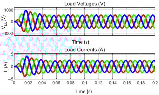
Figure 34.
Load voltage and current of ZSI.
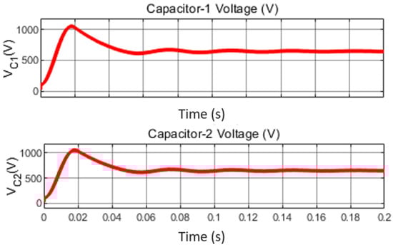
Figure 35.
Z-source capacitor voltages of ZSI.
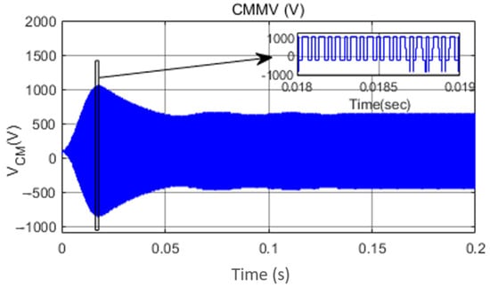
Figure 36.
Common mode voltages of ZSI.
From these results (Figure 21 and Figure 34), it can be understood that peak voltages (956 V in the impedance source inverter and 910 V in the CCBI) and settling time to reach the steady state (0.065 s for the impedance source inverter and 0.021 s for the CCBI) are higher in the case of the impedance source inverter. The peak capacitor voltage is 1124 V in the case of the impedance source inverter, whereas it is 1056 V in the case of the CCBI. It can also be seen that CMMV in the case of the impedance source inverter has a PWM nature, as depicted in Figure 36, whereas it has a steady nature in the case of the CCBI, as depicted in Figure 14. Hence, it can be understood that the CCBI offers better performance for the single-stage power conversion.
In addition, in terms of the number of components, voltage and current THDs, capacitor voltage stresses, and boost factors, the performance of this inverter was compared to that of existing inverter topologies. Figure 37, Figure 38, Figure 39 and Figure 40 provide these comparative characteristics. In comparison to other topologies, the implementation of the CCBI requires fewer components, as seen in Figure 37. As a result, the converter’s cost, size, and volume are reduced. THD (both voltage and current) profiles of the proposed inverter, and the studied inverter topologies, were captured for comparative analysis. It is worth noting that, with the exception of the boost and CCBI topologies, AC filters are utilized on the AC side in all other topologies. The CCBI is able to deliver greater performance in terms of THDs even under these conditions, as seen in Figure 38.
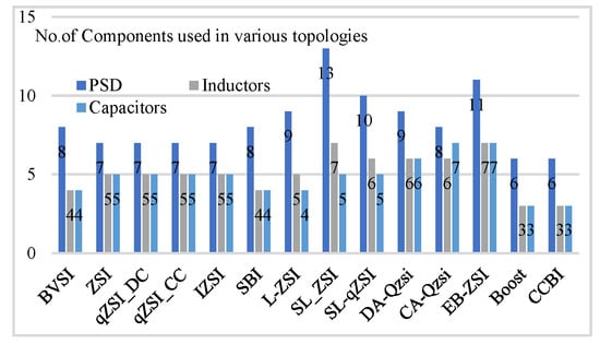
Figure 37.
Bar chart of no. of components used in different topologies.
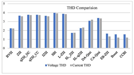
Figure 38.
THD values in different topologies.
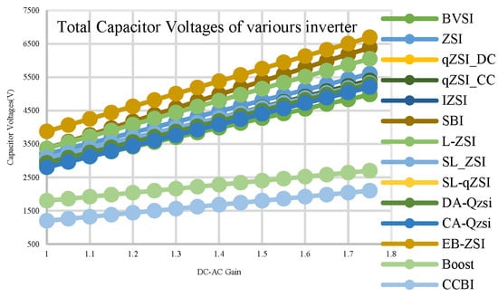
Figure 39.
Total capacitor stress in different topologies.
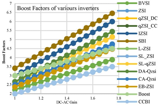
Figure 40.
Boost factors in different topologies.
The total capacitor stresses in the CCBI are quite low as compared to other topologies, as shown in Figure 39. Because the capacitor is the most vulnerable component in an inverter in terms of reliability, reducing voltage stresses on the capacitor improves its reliability. As shown in Figure 40, the proposed converter is capable of providing superior gain than the existing topologies despite having fewer boosting factors. This function aids in the reduction in stresses on the inverter’s capacitors and switches. Overall, the proposed inverters provide higher performance in terms of number of components, voltage and current THDs, capacitor voltage stresses, and boost factors, as evidenced by these comparative data.
Experimentation Results: For the experimental verifications, a laboratory-made test bench was developed, as illustrated in Figure 41. It consists mainly of six IRF460 MOSFETs (500 V, 16 A) driven by a TLP25-based optically isolated driver circuit, three EZPE50506MTA capacitors (15 µF), and three inductors (0.6 mH). Inductor currents and capacitor voltages are sensed by a TELCON-25 and AD202JN-based signal measurement and conditioning circuit.
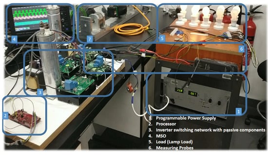
Figure 41.
Prototype of the boost inverter.
The quantities sensed by these sensor-based resistor networks are then applied to the corresponding multiplexer (HEF4052B) input terminals via filtering, amplifying, and biasing circuits. All of the sensed parameters are sent to the FPGA Spartan-3E kit via a multiplexer circuit. Two 2-channel multiplexers are used in time division multiplexing to independently process inductor currents and capacitor voltages. Inductor currents and capacitor voltages are time division multiplexed and processed on the FPGA kit’s on-board ADC (LTC1407A). Internally, these signals are demultiplexed using VHDL code. Using demultiplexed inductor currents and capacitor voltages, a VHDL-programmed sliding mode controller generates gating pulses to the inverter.
This prototype was tested with a 150 V DC supply to demonstrate the proposed inverter’s step-up capability, and the results were monitored in a closed-loop manner, with the control logic developed in an FPGA Sparta-3e XC3S500e board. The CCBI converts 150 V DC to three-phase AC with a peak voltage of 282 volts, 163.29 V (peak) phase voltage, and 4.89 A (peak) phase current. These conversion pole voltages are shown in Figure 42. Load currents are depicted in Figure 43. These findings show that the converter’s performance is consistent with the simulation results. Simulation and hardware tests confirm that the inverter is performing proper DC-AC conversion.
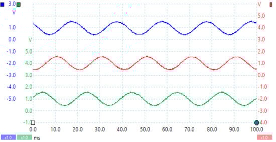
Figure 42.
Pole voltages [300 V/div].
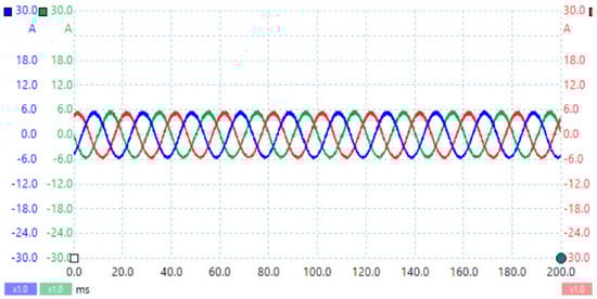
Figure 43.
Load current [1 A/div].
4. Conclusions
This research suggested and successfully validated a unique three-phase, step-up DC-AC converter for distributed power generation using both simulation and experimental data. This converter successfully demonstrated single-stage operation in the same way as any other impedance source converter. Both simulation and experimental results verified that the operating voltages across the capacitors are reduced, resulting in increased capacitor and converter reliability and longevity. In addition to the technology, this inverter offers a lower boosting factor for the necessary DC-AC conversion, thus requiring a lower dc link voltage. When compared to other impedance source converters for the same DC-AC conversion, this feature has a high side gate isolation voltage requirement. In this paper, detailed operations in various modes are presented, along with differential pulse width modulation and a sliding mode controller.
Future work: A performance investigation of the CCBI in electrical vehicle loads with different drive cycles, and in distributed power generation with different environmental conditions, can comprise the future scope of work.
Author Contributions
Writing—original draft and resources, D.R. and P.R.; conceptualisation, methodology, D.R. and P.R.; investigation, D.R., B.L.N. and Y.S.B.; review and editing, D.R., H.H.F. and E.R. All authors have read and agreed to the published version of the manuscript.
Funding
Unitatea Executiva Pentru Finantarea Invatamantului Superior a Cercetarii Dezvoltarii si Inovarii: PN-III-P4-ID-PCE-2020-0008.
Institutional Review Board Statement
Not applicable.
Informed Consent Statement
Not applicable.
Data Availability Statement
Not applicable.
Conflicts of Interest
The authors declare no conflict of interest.
Nomenclature
| Z-source inverter | ZSI |
| Quasi Z-source inverter | q-ZSI |
| Continuous input current quasi Z-source inverter | CICq-ZSI |
| Discontinuous input current quasi Z-source inverter | DICq-ZSI |
| Switched boost inverter | SBI |
| Current-fed switched boost inverter | CF-SBI |
| Quasi SBI | qSBI |
| Improved ZSI | IZSI |
| Pulse width modulation | PWM |
| Total harmonic distortion | THD |
| Capacitor clamped boost inverter | CCBI |
| Boost factor | BF |
| Full-bridge | FB |
| Half-bridge | HB |
| Enhanced boost ZSI | EB-ZSI |
| Diode assisted qZSI | DA-qZSI |
| Capacitor assisted qZSI | CA-qZSI |
| Enhanced boost quasi ZSI | EB-qZSI |
References
- Anderson, J.; Peng, F. A class of quasi-Z-source inverters. In Proceedings of the IEEE IAS’08 Industry Applications Society Annual Meeting, Edmonton, AB, Canada, 5–9 October 2008; pp. 1–7. [Google Scholar]
- Loh, P.C.; Liu, Y.; Abu-Rub, H.; Ge, B.; Blaabjerg, F.; Ellabban, O. Impedance Source Power Electronic Converters; Wiley-IEEE Press: Trenton, NJ, USA, 2016; p. 113. ISBN 978111903710. [Google Scholar]
- Raveendhra, D.; Rajana, P.; Kumar, K.S.R.; Jugge, P.; Devarapalli, R.; Rusu, E.; Fayek, H.H. A High-Gain Multiphase Interleaved Differential Capacitor Clamped Boost Converter. Electronics 2022, 11, 264. [Google Scholar] [CrossRef]
- Shawky, A.; Ahmed, M.; Orabi, M.; El Aroudi, A. Classification of Three-Phase Grid-Tied Microinverters in Photovoltaic Applications. Energies 2020, 13, 2929. [Google Scholar] [CrossRef]
- Hu, X.; Liang, W.; Gao, B.; Ma, P.; Zhang, Y. Integrated step-up non-isolated inverter with leakage current elimination for grid-tied photovoltaic system. IET Power Electron. 2019, 12, 3749–3757. [Google Scholar] [CrossRef]
- Law, K.H. Mathematics Modelling and Simulation of Batteries Charging Capability in Quasi Z Source Impedance Network. In Proceedings of the 2019 7th International Conference on Smart Computing & Communications (ICSCC), Sarawak, Malaysia, 28–30 June 2019; pp. 1–5. [Google Scholar]
- Shen, M.; Wang, J.; Joseph, A.; Peng, F.Z.; Tolbert, L.M.; Adams, D.J. Constant boost control of the Z-source inverter to minimize current ripple and voltage stress. IEEE Trans. Ind. Appl. 2006, 42, 770–778. [Google Scholar] [CrossRef]
- Tang, Y.; Xie, S.; Ding, J. Pulse width modulation of Z-source inverters with minimum inductor current ripple. IEEE Trans. Ind. Electron. 2014, 61, 98–106. [Google Scholar] [CrossRef]
- Mishra, R.S.; Joshi, A. Analysis and PWM control of switched boost inverter. IEEE Trans. Ind. Electron. 2013, 60, 5593–5602. [Google Scholar]
- Nguyen, M.K.; Le, T.V.; Park, S.J.; Lim, Y.C. A class of quasi-switched Boost inverters. IEEE Trans. Ind. Electron. 2015, 62, 1526–1536. [Google Scholar] [CrossRef]
- Nag, S.S.; Mishra, S. Current–Fed Switched Inverter. IEEE Trans. Ind. Electron. 2014, 61, 4680–4690. [Google Scholar] [CrossRef]
- Reddivari, R.; Jena, D. A Correlative Investigation of Impedance Source Networks: A Comprehensive Review. IETE Tech. Rev. 2021, 1, 256–268. [Google Scholar] [CrossRef]
- Qian, W.; Peng, F.Z.; Cha, H. Trans-Z-source inverters. IEEE Trans. Power Electron. 2011, 26, 3453–3463. [Google Scholar] [CrossRef]
- Nguyen, M.K.; Lim, Y.C.; Choi, J.H.; Choi, Y.O. Trans-switched boost inverters. IET Power Electron. 2016, 9, 1065–1073. [Google Scholar] [CrossRef]
- Pan, L. L-Z-Source Inverter. IEEE Trans. Power Electron. 2014, 29, 6534–6543. [Google Scholar] [CrossRef]
- Zhu, M.; Yu, K.; Luo, F.L. Switched inductor Z-source inverter. IEEE Trans. Power Electron. 2010, 25, 2150–2158. [Google Scholar]
- Nguyen, M.K.; Lim, Y.C.; Cho, G.B. Switched-inductor quasi-Z-source inverter. IEEE Trans. Power Electron. 2011, 26, 3183–3191. [Google Scholar] [CrossRef]
- Fathi, H.; Madadi, H. Enhanced-Boost Z-Source Inverters with Switched Z-Impedance. IEEE Trans. Ind. Electron. 2016, 63, 691–703. [Google Scholar] [CrossRef]
- Vinnikov, D.; Roasto, I.; Jalakas, T.; Strzelecki, R.; Adamowicz, M. Analytical comparison between capacitor assisted and diode assisted cascaded quasi-Z-source inverters. Electr. Rev. 2012, 88, 212–217. [Google Scholar]
- Gajanayake, C.J.; Luo, F.L.; Gooi, H.B.; So, P.L.; Siow, L.K. Extended boost Z-source inverters. IEEE Trans. Power Electron. 2010, 25, 2642–2652. [Google Scholar] [CrossRef]
- Jagan, V.; Kotturu, J.; Das, S. Enhanced-Boost Quasi-Z-Source Inverters with Two-Switched Impedance Networks. IEEE Trans. Ind. Electron. 2017, 64, 6885–6897. [Google Scholar] [CrossRef]
- Nguyen, M.; Tran, T.; Lim, Y. A Family of PWM Control Strategies for Single-Phase Quasi-Switched-Boost Inverter. IEEE Trans. Power Electron. 2019, 34, 1458–1469. [Google Scholar] [CrossRef]
- Xiaoquan Zhu, Bo Zhang, Dongyuan Qiu, Enhanced boost quasi-Z-source inverters with active switched-inductor boost network. Power Electron. IET 2018, 11, 1774–1787. [CrossRef]
- Ho, V.; Hyun, J.S.; Chun, T.W.; Lee, H.H. Embedded quasi-Z-source inverters based on active switched-capacitor structure. In Proceedings of the IEEE IECON, 42nd Annual Conference of the IEEE Industrial Electronics Society, Florence, Italy, 23–26 October 2016; pp. 3384–3389. [Google Scholar]
- Ho, V.; Yang, S.G.; Chun, T.W.; Lee, H.H. Topology of modified switched-capacitor Z-source inverters with improved boost capability. In Proceedings of the IEEE Applied Power Electronics Conference and Exposition (APEC), Tampa, FL, USA, 26–30 March 2017; pp. 685–689. [Google Scholar]
- Babaei, E.; Asl, E.S. High voltage gain half-bridge Z-source inverter with low voltage stress on capacitors. IEEE Trans. Ind. Electron. 2017, 64, 191–197. [Google Scholar] [CrossRef]
- Babaei, E.; Asl, E.S.; Babayi, M.H. Steady-state and small-signal analysis of high-voltage gain half-bridge switched boost inverter. IEEE Trans. Ind. Electron. 2016, 63, 3546–3553. [Google Scholar] [CrossRef]
- Asl, E.S.; Babaei, E.; Sabahi, M. High voltage gain half-bridge quasi-switched boost inverter with reduced voltage stress on capacitors. IET Power Electron. 2017, 10, 1095–1108. [Google Scholar] [CrossRef]
- Wang, H.; Liserre, M.; Blaabjerg, F. Toward reliable power electronics—Challenges, design tools and opportunities. IEEE Ind. Electron. Mag. 2013, 7, 17–26. [Google Scholar] [CrossRef] [Green Version]
- Cupertino, A.F.; Lenz, J.M.; Brito, E.M.S.; Pereira, H.A.; Pinheiro, J.R.; Seleme, S.I. Impact of the mission profile length on lifetime prediction of PV inverters. Microelectron. Reliab. 2019, 100–101, 113427. [Google Scholar] [CrossRef]
- Raveendhra, D.; Pathak, M.K. Three-Phase Capacitor Clamped Boost Inverter. IEEE J. Emerg. Sel. Top. Power Electron. 2019, 7, 1999–2011. [Google Scholar] [CrossRef]
Publisher’s Note: MDPI stays neutral with regard to jurisdictional claims in published maps and institutional affiliations. |
© 2022 by the authors. Licensee MDPI, Basel, Switzerland. This article is an open access article distributed under the terms and conditions of the Creative Commons Attribution (CC BY) license (https://creativecommons.org/licenses/by/4.0/).