
A New Type of Architecture of Dye-Sensitized Solar Cells as an Alternative Pathway to Outdoor Photovoltaics

 , ,
, ,
Abstract
1. Introduction
Dye Sensitized Solar Cells
2. Experimental Section
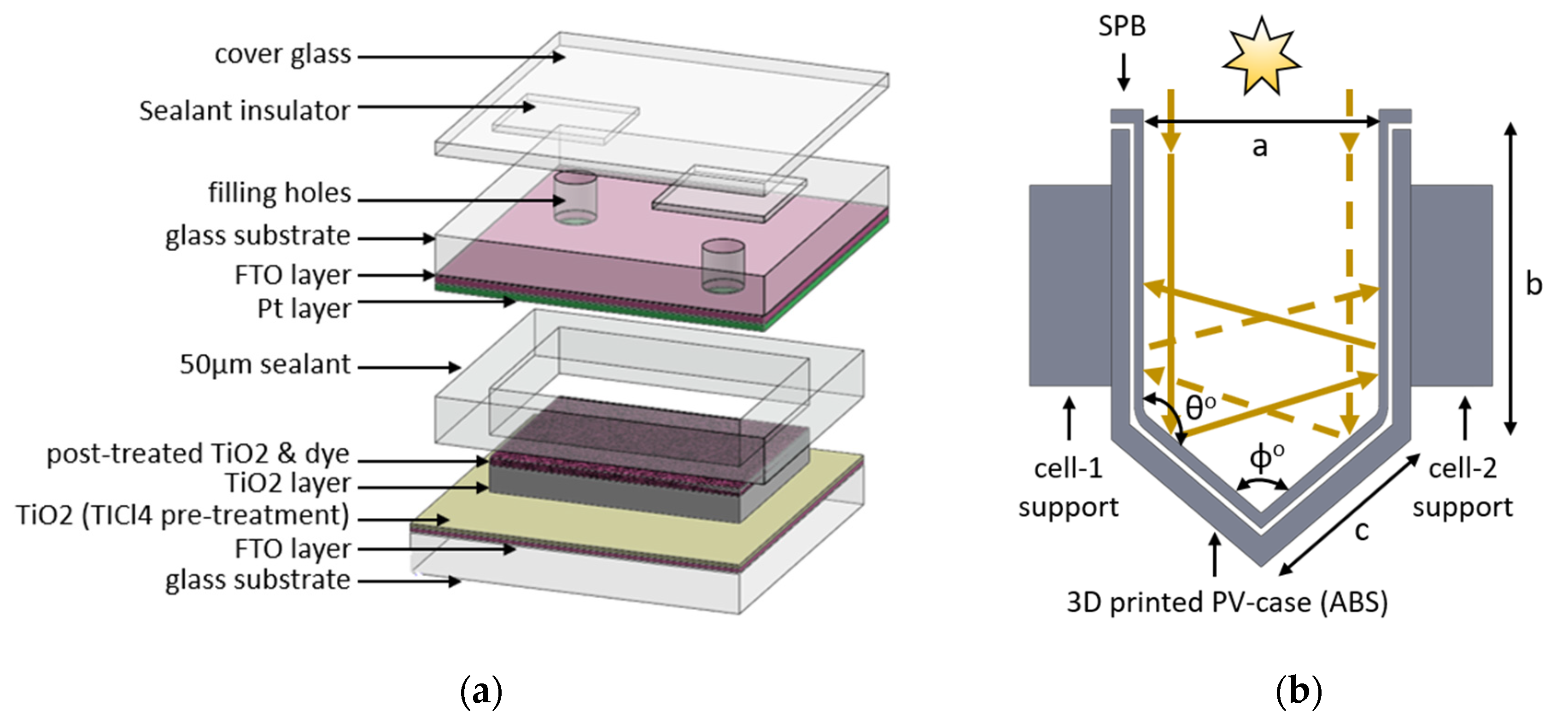
2.1. Materials and Fabrication Methods
2.2. Electrical Characterization
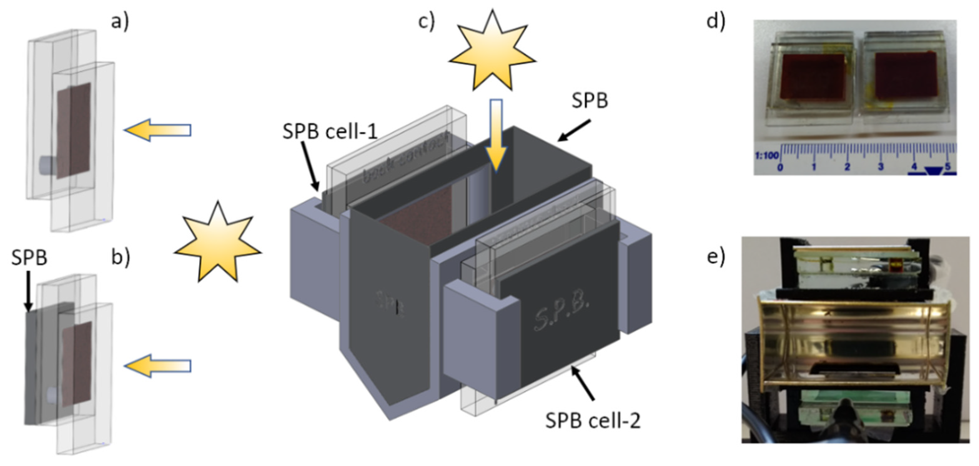
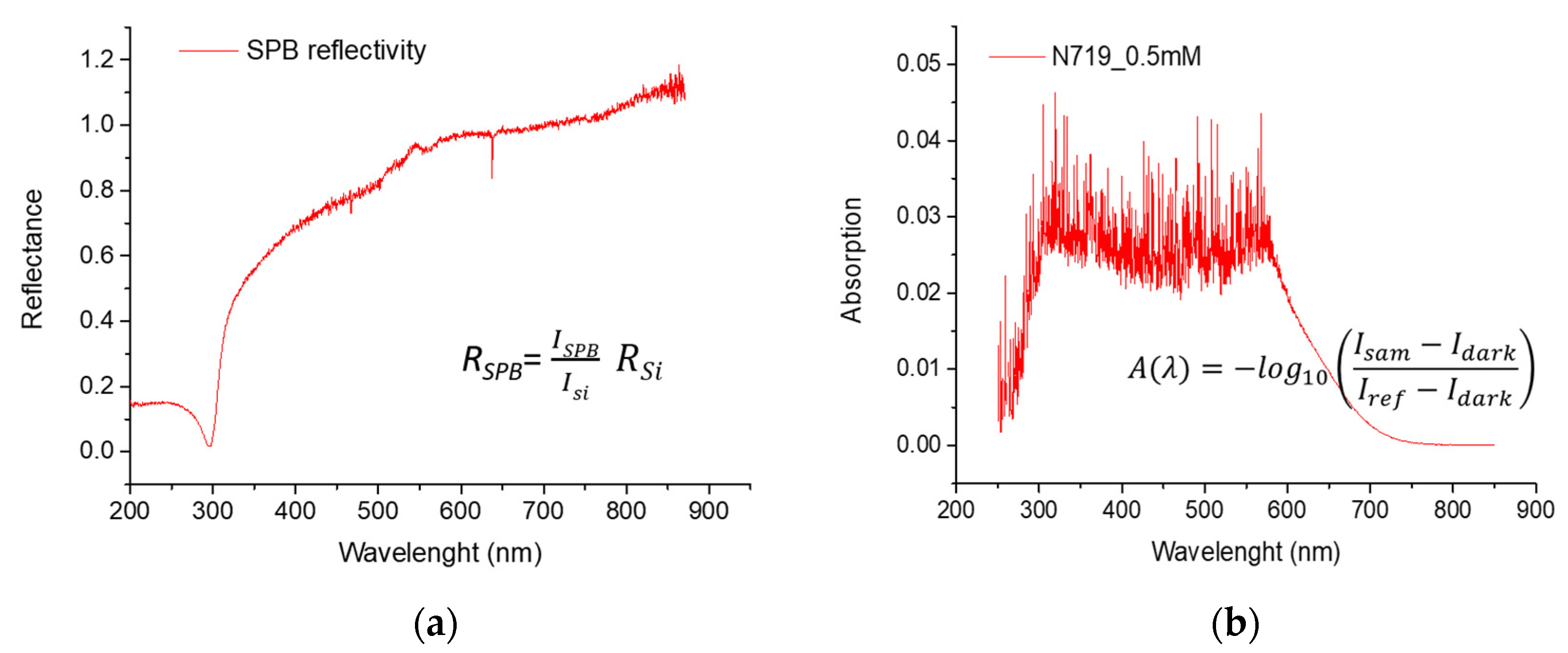
2.3. Experimental Procedure
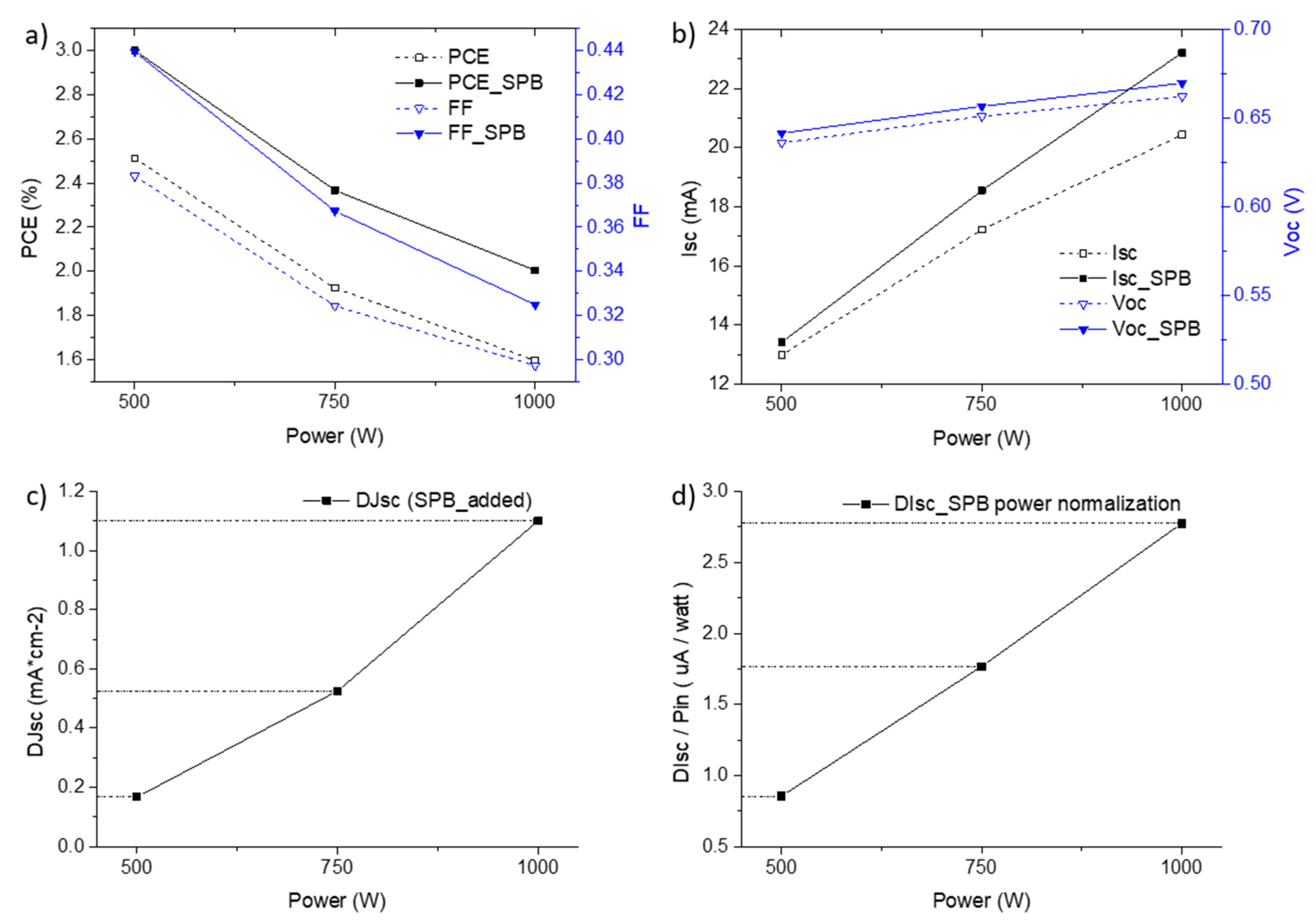
3. Results and Discussion
4. Conclusions
Author Contributions
Funding
Conflicts of Interest
References
- Farinotti, D.; Round, V.; Huss, M.; Compagno, L.; Zekollari, H. Large hydropower and water-storage potential in future glacier-free basins. Nature 2019, 575, 341–344. [Google Scholar] [CrossRef] [PubMed]
- Uihlein, A.; Magagna, D. Wave and tidal current energy—A review of the current state of research beyond technology. Renew. Sustain. Energy Rev. 2016, 58, 1070–1081. [Google Scholar] [CrossRef]
- Kaya, E.; Zarrouk, S.J.; O’Sullivan, M.J. Reinjection in geothermal fields: A review of worldwide experience. Renew. Sustain. Energy Rev. 2011, 15, 47–68. [Google Scholar] [CrossRef]
- Li, J.; Zhou, J.; Chen, B. Review of wind power scenario generation methods for optimal operation of renewable energy systems. Appl. Energy 2020, 280, 115992. [Google Scholar] [CrossRef]
- O’Shaughnessy, E.; Cruce, J.R.; Xu, K. Too much of a good thing? Global trends in the curtailment of solar PV. Sol. Energy 2020, 208, 1068–1077. [Google Scholar] [CrossRef]
- Coelho, L.; Koukou, M.K.; Dogkas, G.; Konstantaras, J.; Vrachopoulos, M.G.; Rebola, A.; Benou, A.; Choropanitis, J.; Karytsas, C.; Sourkounis, C.; et al. Latent Thermal Energy Storage Application in a Residential Building at a Mediterranean Climate. Energies 2022, 15, 1008. [Google Scholar] [CrossRef]
- Garimella, S.; Forinash, D.M.; Boman, D.B. Air-cooled absorbers for extreme-ambient absorption heat pumps. Int. J. Refrig. 2020, 120, 260–270. [Google Scholar] [CrossRef]
- Alizadeh, R.; Lund, P.D.; Soltanisehat, L. Outlook on biofuels in future studies: A systematic literature review. Renew. Sustain. Energy Rev. 2020, 134, 110326. [Google Scholar] [CrossRef]
- Yaashikaa, P.R.; Kumar, P.S.; Saravanan, A.; Varjani, S.; Ramamurthy, R. Bioconversion of municipal solid waste into bio-based products: A review on valorisation and sustainable approach for circular bioeconomy. Sci. Total Environ. 2020, 748, 141312. [Google Scholar] [CrossRef]
- de Castro, C.; Mediavilla, M.; Miguel, L.J.; Frechoso, F. Global solar electric potential: A review of their technical and sustainable limits. Renew. Sustain. Energy Rev. 2013, 28, 824–835. [Google Scholar] [CrossRef]
- Tsao, J.; Lewis, N.; Crabtree, G. Solar FAQs; US Department of Energy: Washington, DC, USA, 2006.
- Jean, J.; Brown, P.; Jaffe, R.; Buonassisi, T.; Bulovic, V. Pathways for Solar Photovoltaics. Energy Environ. Sci. 2015, 8, 1200. [Google Scholar] [CrossRef]
- Geisz, J.F.; France, R.M.; Schulte, K.L.; Steiner, M.A.; Norman, A.G.; Guthrey, H.L.; Young, M.R.; Song, T.; Moriarty, T. Six-junction III–V solar cells with 47.1% conversion efficiency under 143 Suns concentration. Nat. Energy 2020, 5, 326–335. [Google Scholar] [CrossRef]
- Metaferia, W.; Schulte, K.L.; Simon, J.; Johnston, S.; Ptak, A.J. Gallium arsenide solar cells grown at rates exceeding 300 µm h−1 by hydride vapor phase epitaxy. Nat. Commun. 2019, 10, 3361. [Google Scholar] [CrossRef] [PubMed]
- Slade, A.; Garboushian, V. 27.6% Efficient Silicon Concentrator Solar Cells for Mass Production. In Proceedings of the 15th International Photovoltaic Science and Engineering Conference, Shanghai, China, 10–15 October 2005. [Google Scholar]
- Nakamura, M.; Yamaguchi, K.; Kimoto, Y.; Yasaki, Y.; Kato, T.; Sugimoto, H. Cd-Free Cu(In,Ga)(Se,S)2 Thin-Film Solar Cell With Record Efficiency of 23.35%. IEEE J. Photovolt. 2019, 9, 1863–1867. [Google Scholar] [CrossRef]
- The National Renewable Energy Laboratory. Best Research-Cell Efficiency Chart; NREL: Golden, CO, USA, 2020. [Google Scholar]
- Jošt, M.; Jošt, M.; Kegelmann, L.; Korte, L.; Albrecht, S. Monolithic Perovskite Tandem Solar Cells: A Review of the Present Status and Advanced Characterization Methods Toward 30% Efficiency. Adv. Energy Mater. 2020, 10, 1904102. [Google Scholar] [CrossRef]
- Cojocaru, L.; Uchida, S. Determination of unique power conversion efficiency of solar cell showing hysteresis in the I-V curve under various light intensities. Sci. Rep. 2017, 7, 11790. [Google Scholar] [CrossRef]
- De Rossi, F.; Pontecorvo, T.; Brown, T.M. Characterization of photovoltaic devices for indoor light harvesting and customization of flexible dye solar cells to deliver superior efficiency under artificial lighting. Appl. Energy 2015, 156, 413–422. [Google Scholar] [CrossRef]
- Sridhar, N.; Freeman, D. A study of dye sensitized solar cells under indoor and low level outdoor lighting: Comparison to organic and inorganic thin film solar cells and methods to address maximum power point tracking. In Proceedings of the European Photovoltaoc Solar Energy Conference, Austin, TX, USA, 5−8 September 2011. [Google Scholar]
- Venkateswararao, A.; Ho, J.K.W.; So, S.K.; Liu, S.W.; Wong, K.T. Device characteristics and material developments of indoor photovoltaic devices. Mater. Sci. Eng. R Rep. 2020, 139, 100517. [Google Scholar] [CrossRef]
- Lee, C.-P.; Lin, C.A.; Wei, T.C.; Tsai, M.L.; Meng, Y.; Li, C.T.; Ho, K.C.; Wu, C.I.; Lau, S.P.; He, J.H. Economical low-light photovoltaics by using the Pt-free dye-sensitized solar cell with graphene dot/PEDOT:PSS counter electrodes. Nano Energy 2015, 18, 109–117. [Google Scholar] [CrossRef]
- Bărar, A.; Mănăilă-Maximean, D. Ruthenium-based dssc efficiency optimization by graphene quantum dot doping. UPB Sci. Bull. Ser. A Appl. Math. Phys. 2021, 83, 309–316. [Google Scholar]
- Venkatesan, S.; Liu, I.P.; Hung, W.N.; Teng, H.; Lee, Y.L. Highly efficient quasi-solid-state dye-sensitized solar cells prepared by printable electrolytes for room light applications. Chem. Eng. J. 2019, 367, 17–24. [Google Scholar] [CrossRef]
- Venkatesan, S.; Lin, W.H.; Teng, H.; Lee, Y.L. High-Efficiency Bifacial Dye-Sensitized Solar Cells for Application under Indoor Light Conditions. ACS Appl. Mater. Interfaces 2019, 11, 42780–42789. [Google Scholar] [CrossRef]
- Pearl Nightingale, R.H.; Deshpande, M. Indoor photovoltaics and it’s applications. Int. J. Innov. Technol. Explor. Eng. 2019, 9, 4956–4960. [Google Scholar]
- Arbab, A.A.; Ali, M.; Memon, A.A.; Sun, K.C.; Choi, B.J.; Jeong, S.H. An all carbon dye sensitized solar cell: A sustainable and low-cost design for metal free wearable solar cell devices. J. Colloid Interface Sci. 2020, 569, 386–401. [Google Scholar] [CrossRef] [PubMed]
- Arbab, A.A.; Memon, A.A.; Sun, K.C.; Choi, J.Y.; Mengal, N.; Sahito, I.A.; Jeong, S.H. Fabrication of conductive and printable nano carbon ink for wearable electronic and heating fabrics. J. Colloid Interface Sci. 2019, 539, 95–106. [Google Scholar] [CrossRef] [PubMed]
- Yun, S.; Qin, Y.; Uhl, A.R.; Vlachopoulos, N.; Yin, M.; Li, D.; Han, X.; Hagfeldt, A. New-generation integrated devices based on dye-sensitized and perovskite solar cells. Energy Environ. Sci. 2018, 11, 476–526. [Google Scholar] [CrossRef]
- Memon, A.A.; Arbab, A.A.; Sahito, I.A.; Sun, K.C.; Mengal, N.; Jeong, S.H. Synthesis of highly photo-catalytic and electro-catalytic active textile structured carbon electrode and its application in DSSCs. Sol. Energy 2017, 150, 521–531. [Google Scholar] [CrossRef]
- Sahito, I.A.; Sun, K.C.; Arbab, A.A.; Qadir, M.B.; Choi, Y.S.; Jeong, S.H. Flexible and conductive cotton fabric counter electrode coated with graphene nanosheets for high efficiency dye sensitized solar cell. J. Power Sources 2016, 319, 90–98. [Google Scholar] [CrossRef]
- Chae, Y.; Lee, H.; Wang, P.K. Flexible solar textiles with style for future smart clothing system. In Proceedings of the Fiber Society 2016 Spring Conference: Textile Innovations—Opportunities and Challenges, Mulhouse, France, 25–27 May 2016. [Google Scholar]
- Mainville, M.; Leclerc, M. Recent Progress on Indoor Organic Photovoltaics: From Molecular Design to Production Scale. ACS Energy Lett. 2020, 5, 1186–1197. [Google Scholar] [CrossRef]
- Liu, J.; Cui, Y.; Zu, Y.; An, C.; Xu, B.; Yao, H.; Zhang, S.; Hou, J. Organic photovoltaic cells for low light applications offering new scope and orientation. Org. Electron. 2020, 85, 105798. [Google Scholar] [CrossRef]
- Hou, X.; Wang, Y.; Lee, H.K.H.; Datt, R.; Uslar, M.; Yan, D.; Li, M.; Zhu, F.; Hou, B.; Tsoi, W.C.; et al. Indoor application of emerging photovoltaics—progress, challenges and perspectives. J. Mater. Chem. A 2020, 8, 21503–21525. [Google Scholar] [CrossRef]
- Zhu, Z.; Mao, K.; Xu, J. Perovskite tandem solar cells with improved efficiency and stability. J. Energy Chem. 2020, 58, 219–232. [Google Scholar] [CrossRef]
- Xie, S.; Xia, R.; Chen, Z.; Tian, J.; Yan, L.; Ren, M.; Li, Z.; Zhang, G.; Xue, Q.; Yip, H.L.; et al. Efficient monolithic perovskite/organic tandem solar cells and their efficiency potential. Nano Energy 2020, 78, 105238. [Google Scholar] [CrossRef]
- Wang, J.; Wang, J.; Zardetto, V.; Datta, K.; Zhang, D.; Wienk, M.M.; Janssen, R.A.J. 16.8% Monolithic all-perovskite triple-junction solar cells via a universal two-step solution process. Nat. Commun. 2020, 11, 5254. [Google Scholar] [CrossRef] [PubMed]
- Aydin, E.; Allen, T.G.; De Bastiani, M.; Xu, L.; Ávila, J.; Salvador, M.; Van Kerschaver, E.; De Wolf, S. Interplay between temperature and bandgap energies on the outdoor performance of perovskite/silicon tandem solar cells. Nat. Energy 2020, 5, 851–859. [Google Scholar] [CrossRef]
- Moses, G.; Huang, X.; Zhao, Y.; Auf der Maur, M.; Katz, E.A.; Gordon, J.M. InGaN/GaN multi-quantum-well solar cells under high solar concentration and elevated temperatures for hybrid solar thermal-photovoltaic power plants. Prog. Photovolt. Res. Appl. 2020, 28, 1167–1174. [Google Scholar] [CrossRef]
- Zhou, Z.; Jiang, C.; Huang, H.; Liang, L.; Zhu, G. Three-junction tandem photovoltaic cell for a wide temperature range based on a multilayer circular truncated cone metamaterial emitter. Energy 2020, 210, 118503. [Google Scholar] [CrossRef]
- Zhang, X.; Knize, R.J.; Lu, Y. Enhanced light absorption in thin-film tandem solar cells using a bottom metallic nanograting. Appl. Phys. A 2014, 115, 509–515. [Google Scholar] [CrossRef]
- Schneider, B.W.; Lal, N.N.; Baker-Finch, S.; White, T.P. Pyramidal surface textures for light trapping and antireflection in perovskite-on-silicon tandem solar cells. Opt. Express 2014, 22, A1422–A1430. [Google Scholar] [CrossRef]
- Shi, D.; Zeng, Y.; Shen, W. Perovskite/c-Si tandem solar cell with inverted nanopyramids: Realizing high efficiency by controllable light trapping. Sci. Rep. 2015, 5, 16504. [Google Scholar] [CrossRef]
- Kumar, K.; Das, A.; Kumawat, U.K.; Dhawan, A. Tandem organic solar cells containing plasmonic nanospheres and nanostars for enhancement in short circuit current density. Opt. Express 2019, 27, 31599–31620. [Google Scholar] [CrossRef] [PubMed]
- You, J.; Dou, L.; Yoshimura, K.; Kato, T.; Ohya, K.; Moriarty, T.; Emery, K.; Chen, C.C.; Gao, J.; Li, G.; et al. A polymer tandem solar cell with 10.6% power conversion efficiency. Nat. Commun. 2013, 4, 1446. [Google Scholar] [CrossRef] [PubMed]
- Amran, A.-A.; Eike, K.; Bor, L.; Artiom, M.; Hannes, H.; Pietro, C.; José, A.M.; Anna, B.M.V.; Ernestas, K.; Joel, A.S.; et al. Monolithic perovskite/silicon tandem solar cell with >29% efficiency by enhanced hole extraction. Science 2020, 370, 1300–1309. [Google Scholar]
- Barar, A.; Manaila-Maximean, D.; Danila, O.; Vladescu, M. Parameter extraction of an organic solar cell using asymptotic estimation and Lambert W function. In Proceedings of the SPIE—The International Society for Optical Engineering, Constanta, Romania, 25–28 September 2016. [Google Scholar]
- van Dijk, L.; Paetzold, U.W.; Blab, G.A.; Schropp, R.E.I.; di Vece, M. 3D-printed external light trap for solar cells. Prog. Photovolt. Res. Appl. 2016, 24, 623–633. [Google Scholar] [CrossRef] [PubMed]
- van Dijk, L.; Marcus, E.A.P.; Oostra, A.J.; Schropp, R.E.I.; Di Vece, M. 3D-printed concentrator arrays for external light trapping on thin film solar cells. Sol. Energy Mater. Sol. Cells 2015, 139, 19–26. [Google Scholar] [CrossRef]
- O’Regan, B.; Grätzel, M. A low-cost, high-efficiency solar cell based on dye-sensitized colloidal TiO2 films. Nature 1991, 353, 737–740. [Google Scholar] [CrossRef]
- Chou, J.; Chu, C.; Liao, Y.; Huang, C.; Lin, Y.; Wu, H.; Nien, Y. Fabrication and Photovoltaic Properties of Dye-Sensitized Solar Cells Modified by Graphene Oxide and Magnetic Bead. IEEE Electron Device Lett. 2015, 36, 711–713. [Google Scholar] [CrossRef]
- Khalifa, A.; Shafie, S.; Hasan, W.Z.W.; Lim, H.N.; Rusop, M.; Pandey, S.S.; Vats, A.K.; AlSultan, H.A.; Samaila, B. Comprehensive performance analysis of dye-sensitized solar cells using single layer TiO2 photoanode deposited using screen printing technique. Optik 2020, 223, 165595. [Google Scholar] [CrossRef]
- Xie, M.; Chen, J.; Wang, J.; Kong, C.P.; Bai, F.Q.; Jia, R.; Zhang, H.X. Exploring the sensitization properties of thienyl-functionalized tripyrrole Ru(II) complexes on TiO2 (101) surface: A theoretical study. Theor. Chem. Acc. 2015, 134, 44. [Google Scholar] [CrossRef]
- Yan, W.; Jiang, D.; Guo, W.; Zhou, F. Efficiency enhancement of solid-state dye-sensitized solar cells by doping polythiophene films photoelectrochemically grown onto TiO2 nanoparticles covered with cis-bis(isothiocyanato) bis(2,2′-bipyridyl-4,4′-dicarboxylato)ruthenium(II). Electrochim. Acta 2020, 355, 136685. [Google Scholar] [CrossRef]
- Chen, C.-Y.; Wang, M.; Li, J.-Y.; Pootrakulchote, N.; Alibabaei, L.; Ngoc-le, C.-h.; Decoppet, J.-D.; Tsai, J.-H.; Grätzel, C.; Wu, C.-G.; et al. Highly Efficient Light-Harvesting Ruthenium Sensitizer for Thin-Film Dye-Sensitized Solar Cells. ACS Nano 2009, 3, 3103–3109. [Google Scholar] [CrossRef] [PubMed]
- Yu, Q.; Wang, Y.; Yi, Z.; Zu, N.; Zhang, J.; Zhang, M.; Wang, P. High-Efficiency Dye-Sensitized Solar Cells: The Influence of Lithium Ions on Exciton Dissociation, Charge Recombination, and Surface States. ACS Nano 2010, 4, 6032–6038. [Google Scholar] [CrossRef] [PubMed]
- Bach, U.; Krueger, J.; Graetzel, M. Concept of Dye-Sensitized Mesoporous Solid State Heterojunction Solar Cells. In Proceedings of the International Symposium on Optical Science and Technology, San Diego, CA, USA, 30 July 2000; Volume 4108. [Google Scholar]
- Sarker, S.; Seo, H.W.; Jin, Y.K.; Aziz, M.A.; Kim, D.M. Transparent conducting oxides and their performance as substrates for counter electrodes of dye-sensitized solar cells. Mater. Sci. Semicond. Process. 2019, 93, 28–35. [Google Scholar] [CrossRef]
- More, V.; Shivade, V.; Bhargava, P. Effect of Cleaning Process of Substrate on the Efficiency of the DSSC. Trans. Indian Ceram. Soc. 2016, 75, 59–62. [Google Scholar] [CrossRef]
- Syrrokostas, G.; Leftheriotis, G.; Yianoulis, P. Effect of acidic additives on the structure and performance of TiO2 films prepared by a commercial nanopowder for dye-sensitized solar cells. Renew. Energy 2014, 72, 164–173. [Google Scholar] [CrossRef]
- Park, K.-H.; Jin, E.M.; Gu, H.B.; Shim, S.E.; Hong, C.K. Effects of HNO3 treatment of TiO2 nanoparticles on the photovoltaic properties of dye-sensitized solar cells. Mater. Lett. 2009, 63, 2208–2211. [Google Scholar] [CrossRef]
- Radwan, I.M.; Taya, S.; El-Agez, T.M.; Abdel-latif, M.; Saleh, H. Improvement of the Performance of Purple Carrot Sensitized Solar Cells by Acidic Treatment of FTO Glass Substrate and TiO 2 Film. Acta Phys. Pol. A 2016, 130, 795–799. [Google Scholar] [CrossRef]
- Sedghi, A.; Miankushki, H.N. Influence of TiCl4Treatment on Structure and Performance of Dye-Sensitized Solar Cells. Jpn. J. Appl. Phys. 2013, 52, 075002. [Google Scholar] [CrossRef]
- Ito, S.; Murakami, T.N.; Comte, P.; Liska, P.; Grätzel, C.; Nazeeruddin, M.K.; Grätzel, M. Fabrication of thin film dye sensitized solar cells with solar to electric power conversion efficiency over 10%. Thin Solid Films 2008, 516, 4613–4619. [Google Scholar] [CrossRef]
- Sommeling, P.M.; O'Regan, B.C.; Haswell, R.R.; Smit, H.J.P.; Bakker, N.J.; Smits, J.J.T.; Kroon, J.M.; Van Roosmalen, J.A. Influence of a TiCl4 Post-Treatment on Nanocrystalline TiO2 Films in Dye-Sensitized Solar Cells. J. Phys. Chem. B 2006, 110, 19191–19197. [Google Scholar] [CrossRef]
- Nurosyid, F.; Furqoni, L.; Supriyanto, A.; Suryana, R. Effect of screen printing type on transparent TiO2 layer as the working electrode of dye sensitized solar cell (DSSC) for solar windows applications. J. Phys. Conf. Ser. 2016, 776, 012011. [Google Scholar] [CrossRef]
- Huang, A.-N.; Pien, W.-C.; Kuo, H.-P. Preparation of the Working Electrode of Dye-sensitized Solar Cells Using Screen Printing with Alkyd Resins. Energy Procedia 2014, 61, 1528–1531. [Google Scholar] [CrossRef][Green Version]
- Ito, S.; Chen, P.; Comte, P.; Nazeeruddin, M.K.; Liska, P.; Péchy, P.; Grätzel, M. Fabrication of screen-printing pastes from TiO2 powders for dye-sensitised solar cells. Prog. Photovolt. Res. Appl. 2007, 15, 603–612. [Google Scholar] [CrossRef]
- Carnie, M.; Watson, T.; Worsley, D. UV Filtering of Dye-Sensitized Solar Cells: The Effects of Varying the UV Cut-Off upon Cell Performance and Incident Photon-to-Electron Conversion Efficiency. Int. J. Photoenergy 2012, 2012, 506132. [Google Scholar] [CrossRef]
- Carnie, M.; Bryant, D.; Watson, T.; Worsley, D. Photocatalytic Oxidation of Triiodide in UVA-Exposed Dye-Sensitized Solar Cells. Int. J. Photoenergy 2012, 2012, 524590. [Google Scholar] [CrossRef]
- Ma, L.; Xu, L.; Zhang, K.; Wu, W.; Ma, Z. The measurement of series and shunt resistances of the silicon solar cell based on LabVIEW. In Proceedings of the 2011 International Conference on Electrical and Control Engineering, Yichang, China, 16–18 September 2011. [Google Scholar]
- Luque, A.; Hegedus, S. Handbook of Photovoltaic Science and Engineering; Wiley: Hoboken, NJ, USA, 2003. [Google Scholar]
- Safriani, L.; Nurrida, A.; Mulyana, C.; Susilawati, T.; Bahtiar, A.; Aprilia, A. Calculation of DSSC parameters based on ZnO nanorod/TiO2 mesoporous photoanode. IOP Conf. Ser. Earth Environ. Sci. 2017, 75, 012004. [Google Scholar] [CrossRef]


| Dye | Number of Cells | Active Area (cm2) | Pin (watt/m2) | Best Performance | ||
|---|---|---|---|---|---|---|
| FF | PCE (%) | Jsc (Max) (mA/cm2) | ||||
| N719 | 46 | 2.52 | 1000 | 0.33 | 3.06 | 9.9 |
| N749 | 7 | 2.52 | 1000 | 0.36 | 2.23 | 13.4 |
| DSSC | Pin (watt) | Active Area (cm2) | PCE (%) | FF | Isc (mA) | Voc (V) | Jsc (mA/cm2) |
|---|---|---|---|---|---|---|---|
| Cell (Ν719) | 500 | 2.52 | 2.51 | 0.38 | 12.98 | 0.64 | 5.15 |
| 750 | 2.52 | 1.92 | 0.32 | 17.23 | 0.65 | 6.84 | |
| 1000 | 2.52 | 1.60 | 0.29 | 20.44 | 0.66 | 8.11 | |
| SPB cell (Ν719) | 500 | 2.52 | 2.99 | 0.44 | 13.41 | 0.64 | 5.32 |
| 750 | 2.52 | 2.37 | 0.37 | 18.55 | 0.66 | 7.36 | |
| 1000 | 2.52 | 2.00 | 0.32 | 23.21 | 0.67 | 9.21 |
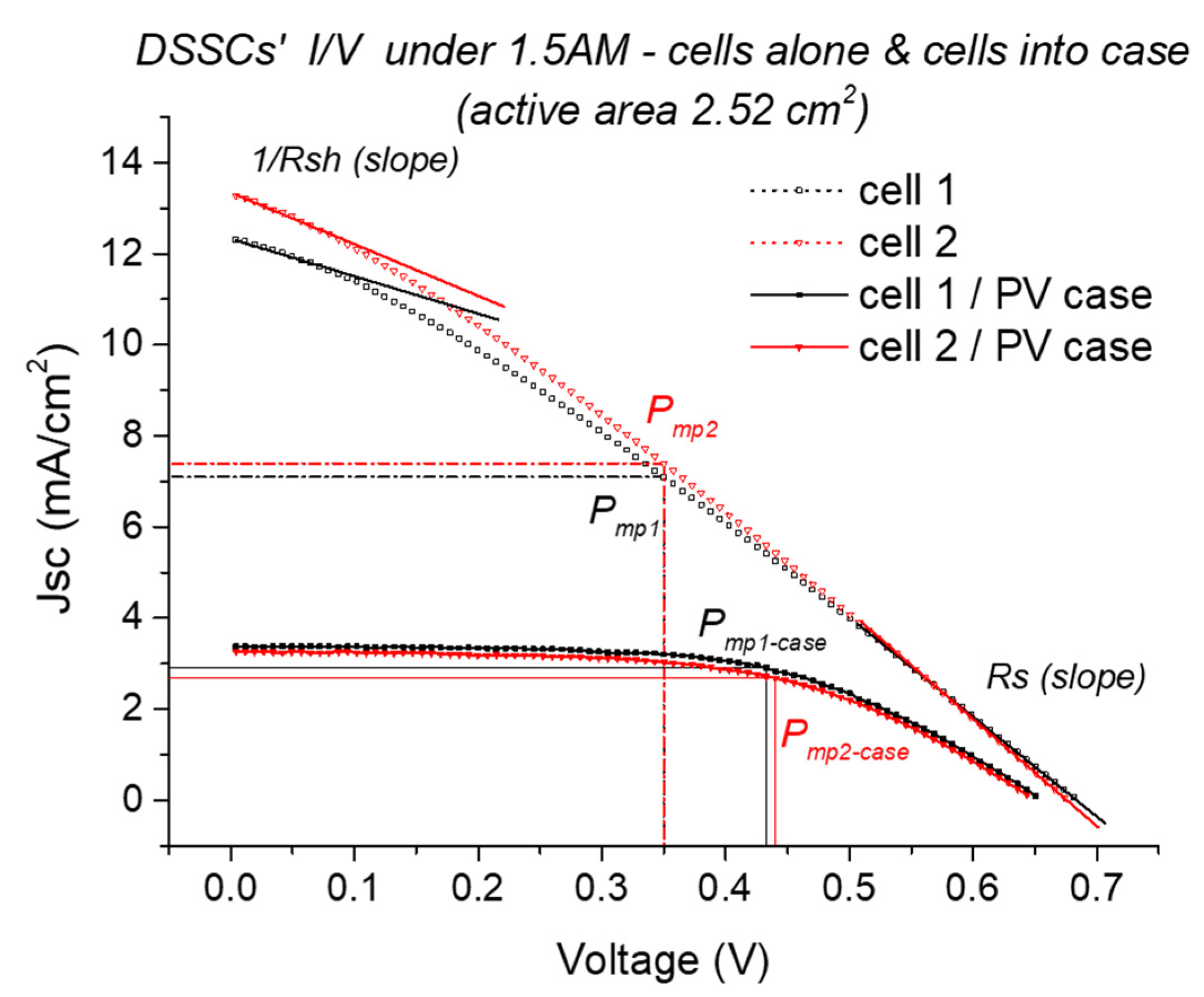
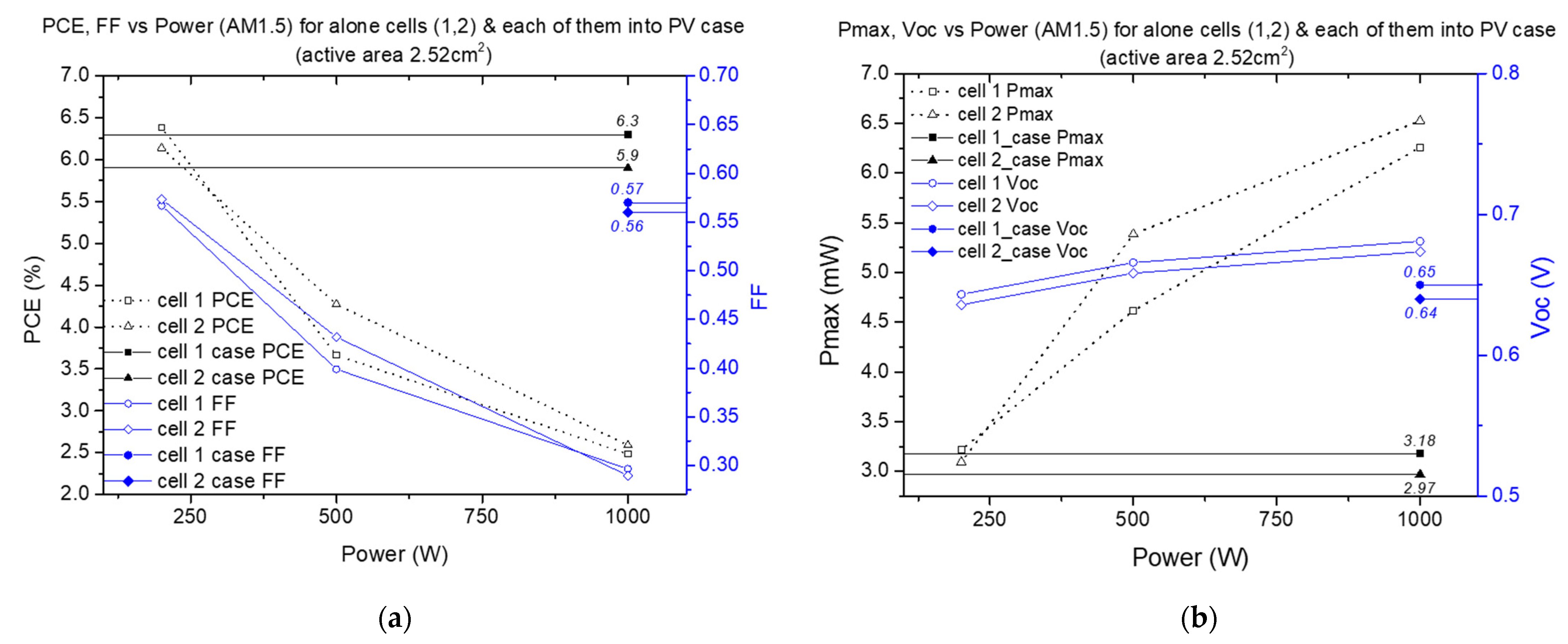
| DSSC | Pin (watt) | Active Area (cm2) | Voc (V) | Jsc (mA/cm2) | PCE (%) | FF | Pmax (mW) |
|---|---|---|---|---|---|---|---|
| cell 1 | 200 | 2.52 | 0.64 | 3.50 | 6.38 | 0.57 | 3.22 |
| 500 | 2.52 | 0.67 | 6.90 | 3.67 | 0.40 | 4.62 | |
| 1000 | 2.52 | 0.68 | 12.31 | 2.48 | 0.30 | 6.26 | |
| cell 2 | 200 | 2.52 | 0.64 | 3.37 | 6.14 | 0.57 | 3.09 |
| 500 | 2.52 | 0.66 | 7.52 | 4.27 | 0.43 | 5.39 | |
| 1000 | 2.52 | 0.67 | 13.27 | 2.59 | 0.29 | 6.53 | |
| cell 1 PV case | 1000 | 2.52 | 0.65 | 3.38 | 6.30 | 0.57 | 3.18 |
| cell 2 PV case | 1000 | 2.52 | 0.64 | 3.27 | 5.90 | 0.56 | 2.97 |
Publisher’s Note: MDPI stays neutral with regard to jurisdictional claims in published maps and institutional affiliations. |
© 2022 by the authors. Licensee MDPI, Basel, Switzerland. This article is an open access article distributed under the terms and conditions of the Creative Commons Attribution (CC BY) license (https://creativecommons.org/licenses/by/4.0/).
Share and Cite
Prouskas, C.; Mourkas, A.; Zois, G.; Lidorikis, E.; Patsalas, P. A New Type of Architecture of Dye-Sensitized Solar Cells as an Alternative Pathway to Outdoor Photovoltaics. Energies 2022, 15, 2486. https://doi.org/10.3390/en15072486
Prouskas C, Mourkas A, Zois G, Lidorikis E, Patsalas P. A New Type of Architecture of Dye-Sensitized Solar Cells as an Alternative Pathway to Outdoor Photovoltaics. Energies. 2022; 15(7):2486. https://doi.org/10.3390/en15072486
Chicago/Turabian StyleProuskas, Costas, Angelos Mourkas, Georgios Zois, Elefterios Lidorikis, and Panos Patsalas. 2022. "A New Type of Architecture of Dye-Sensitized Solar Cells as an Alternative Pathway to Outdoor Photovoltaics" Energies 15, no. 7: 2486. https://doi.org/10.3390/en15072486
APA StyleProuskas, C., Mourkas, A., Zois, G., Lidorikis, E., & Patsalas, P. (2022). A New Type of Architecture of Dye-Sensitized Solar Cells as an Alternative Pathway to Outdoor Photovoltaics. Energies, 15(7), 2486. https://doi.org/10.3390/en15072486