


Analysis and Design of a High-Efficiency SiC MOSFET 6-Phase Boost Rectifier


Abstract
1. Introduction
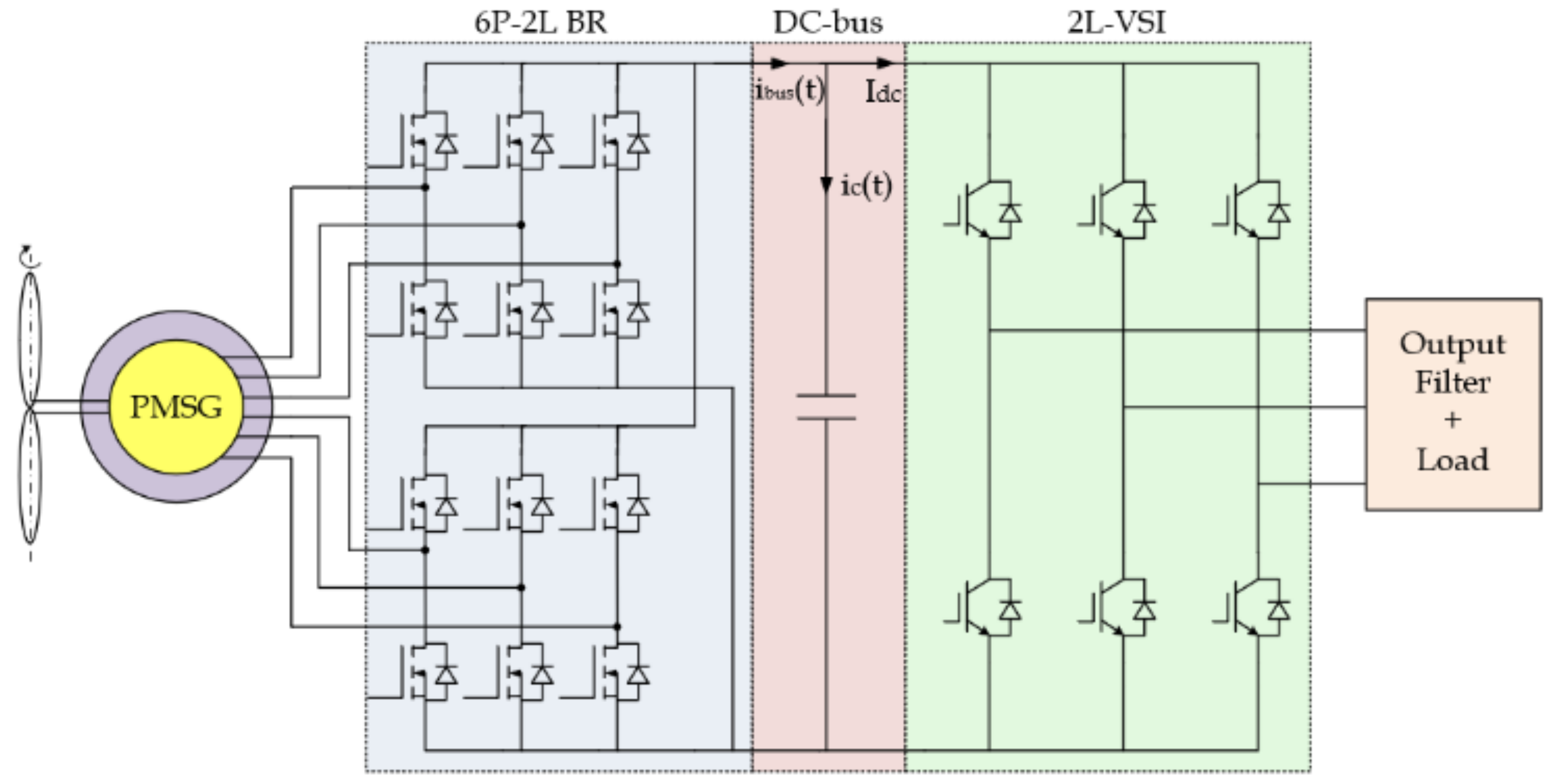
2. 6-Phase Power Conversion System Design
- Voltage rating and current rating to select proper power semiconductor devices;
- Power loss distribution for the selected power semiconductor devices;
- DC-bus current stress and voltage ripple to select an appropriate DC-bus configuration;
- Thermal sizing to evaluate the minimum thermal resistance in order to opt for a suitable heatsink.
2.1. Voltage Rating and Current Rating
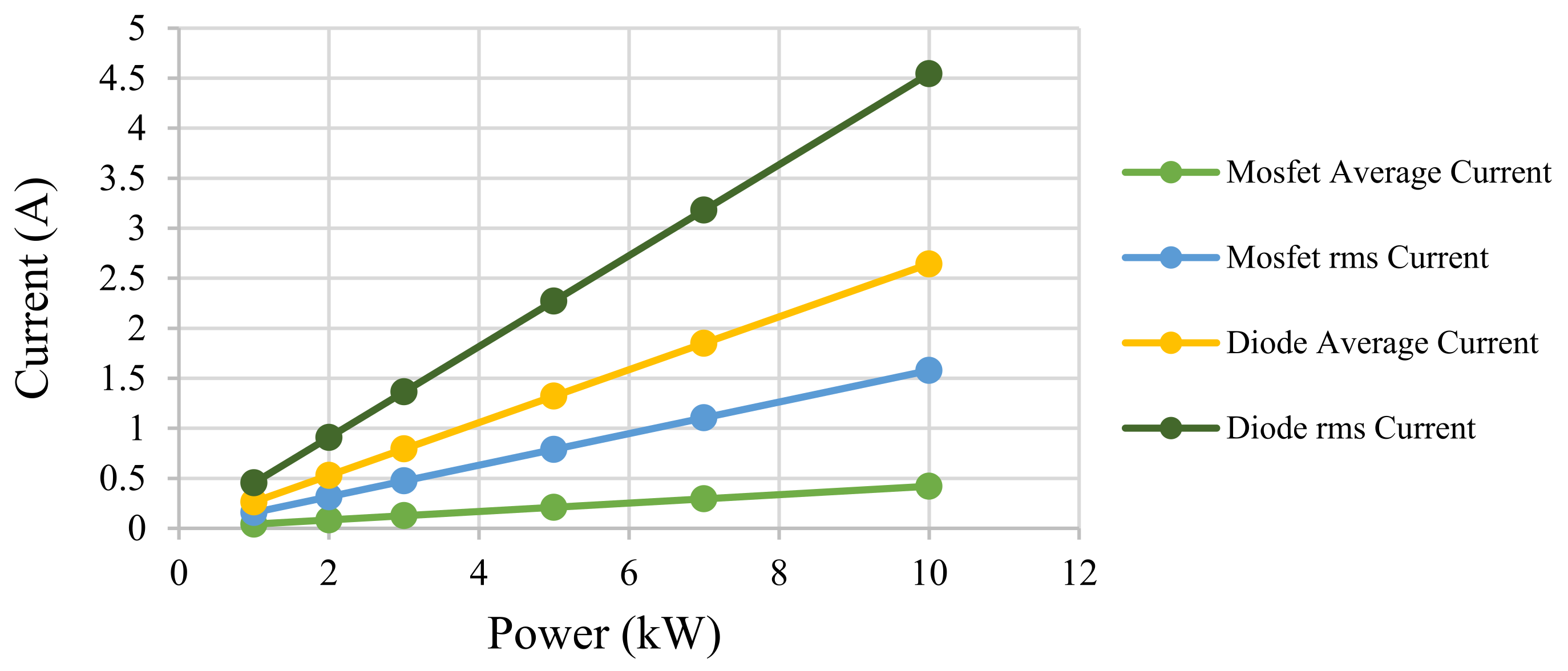
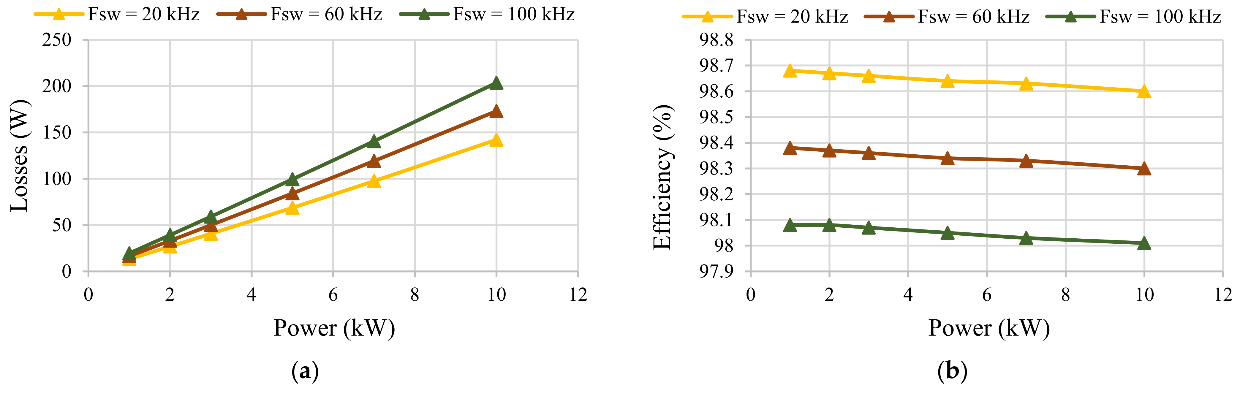
2.2. Power Loss Distribution
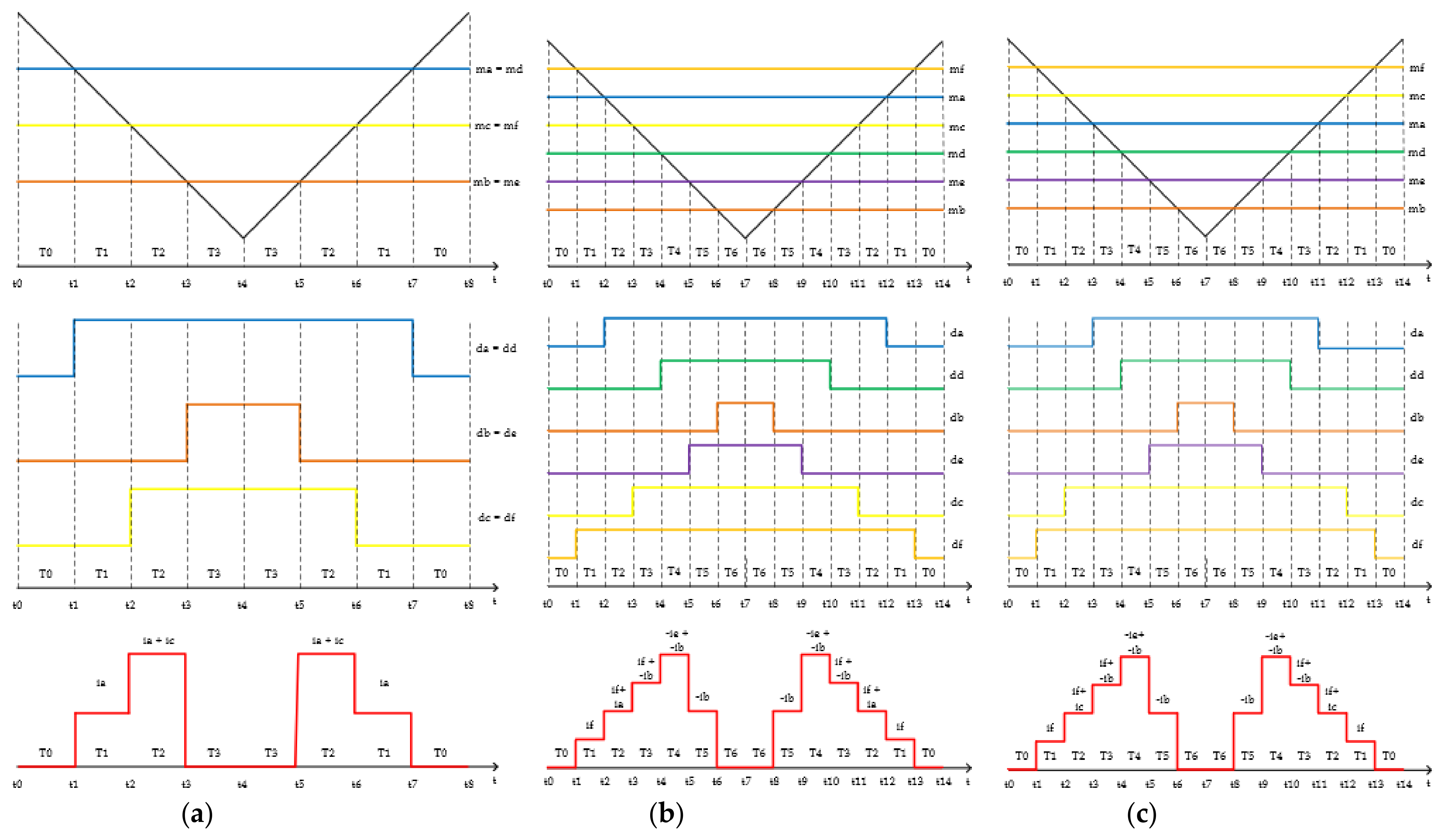
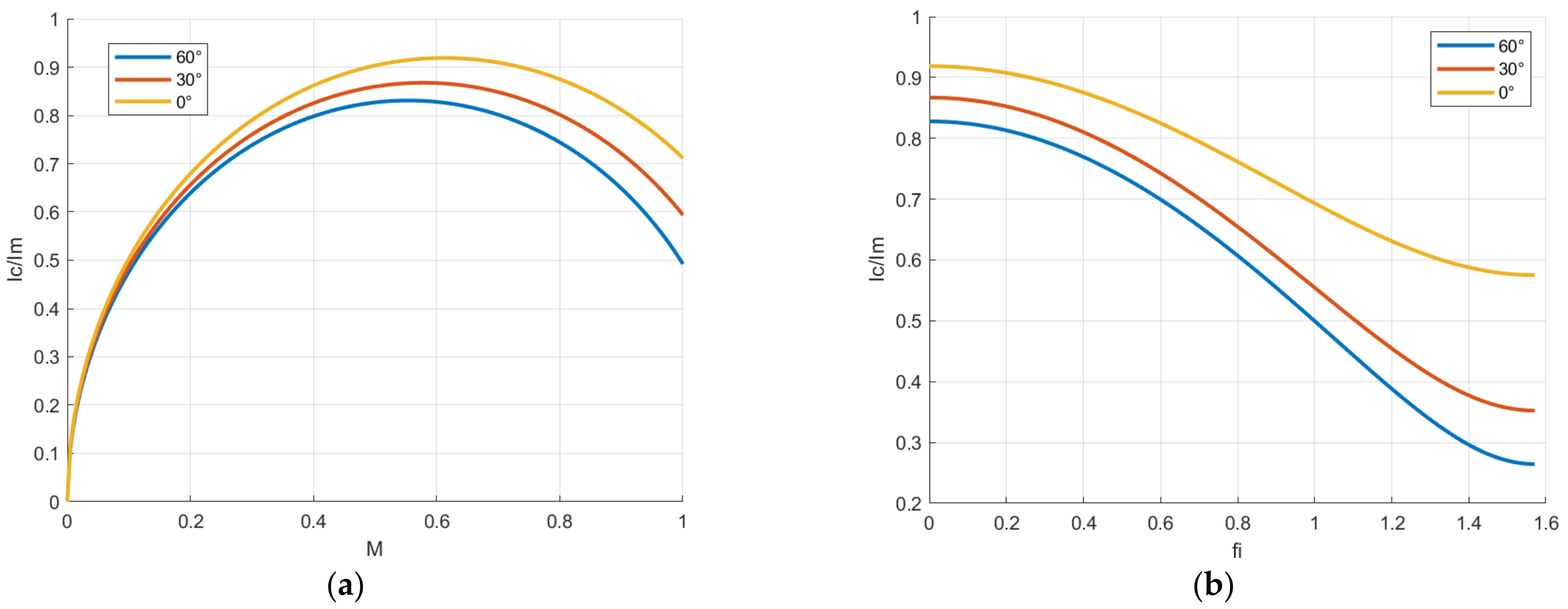
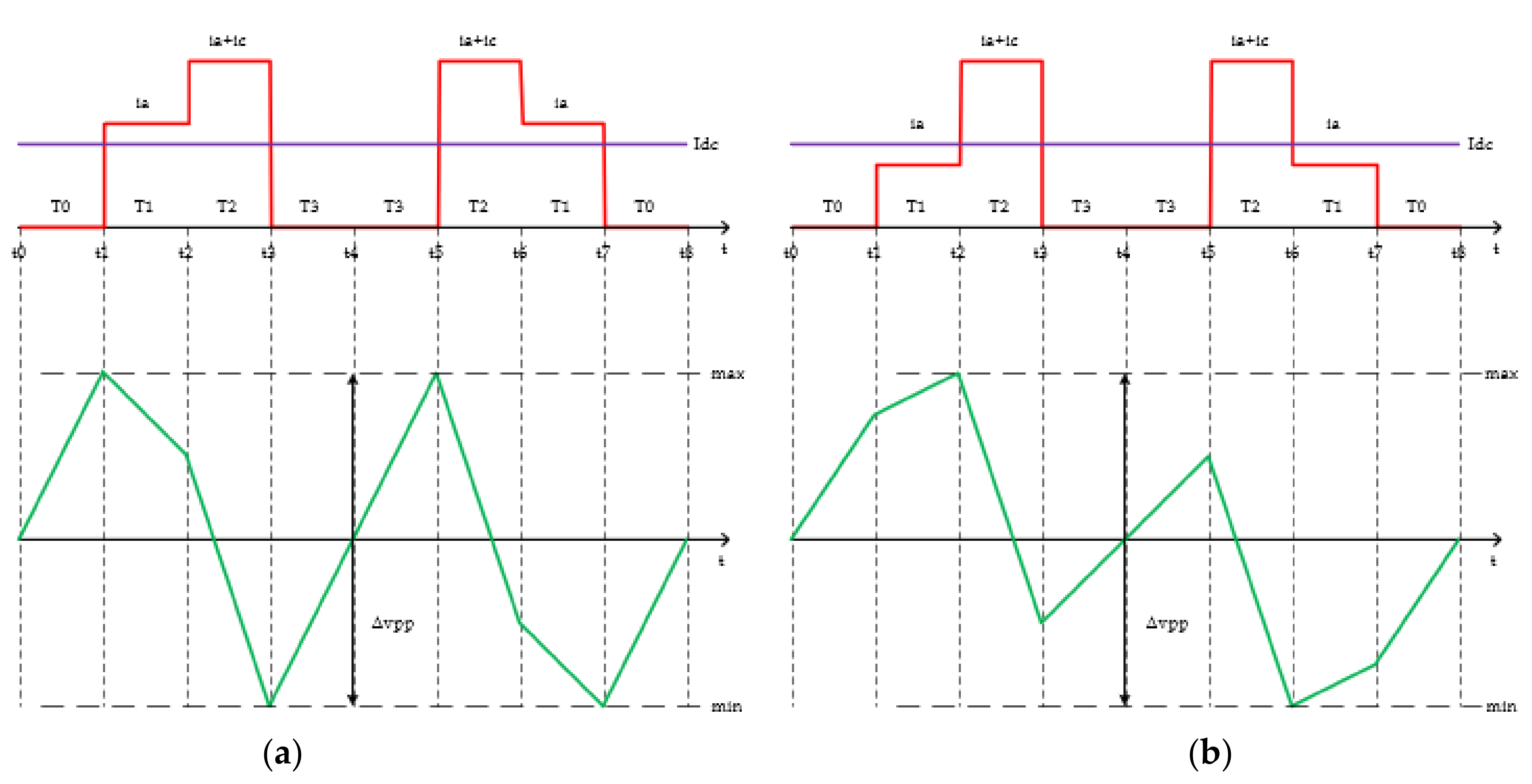
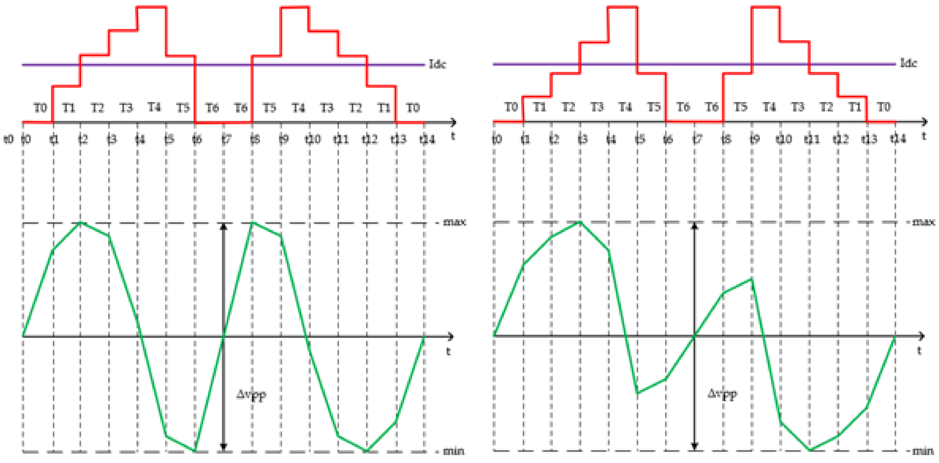
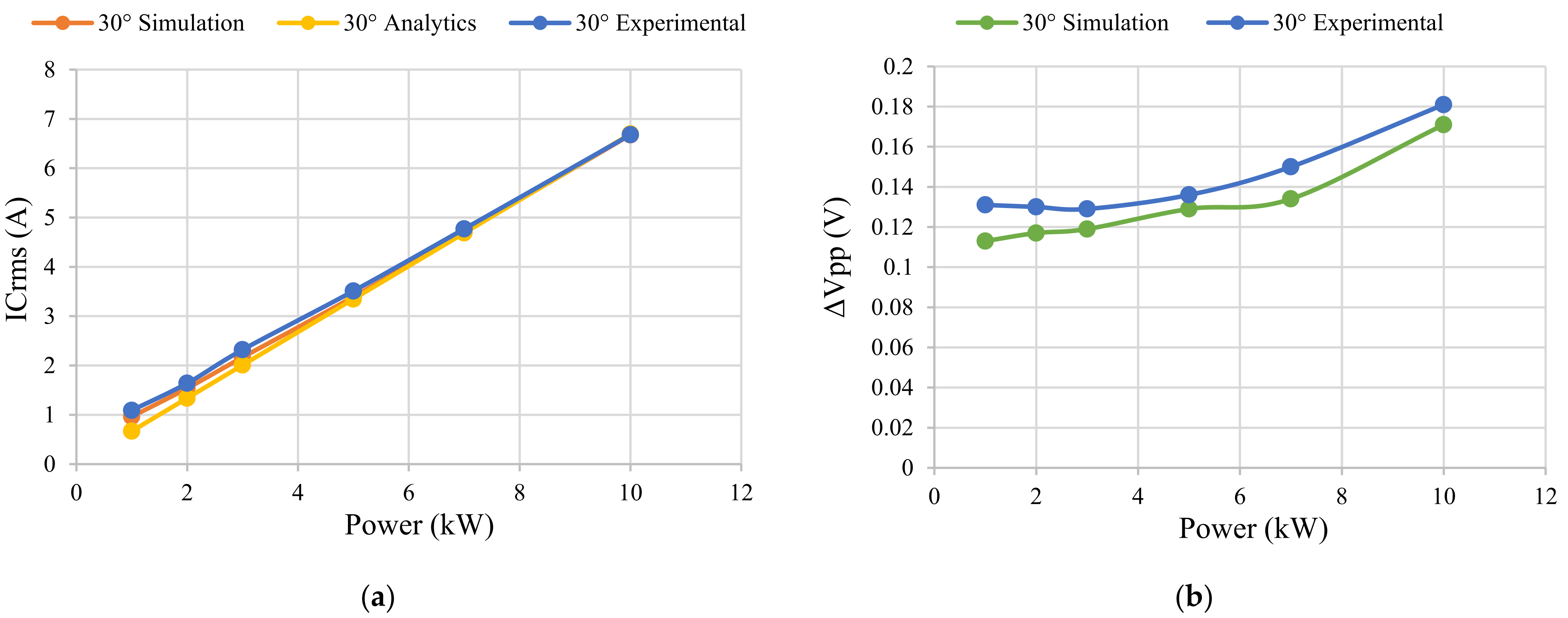
2.3. DC-Bus Design
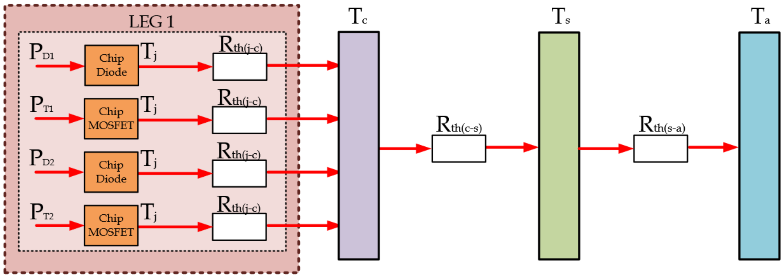
2.4. Thermal Sizing
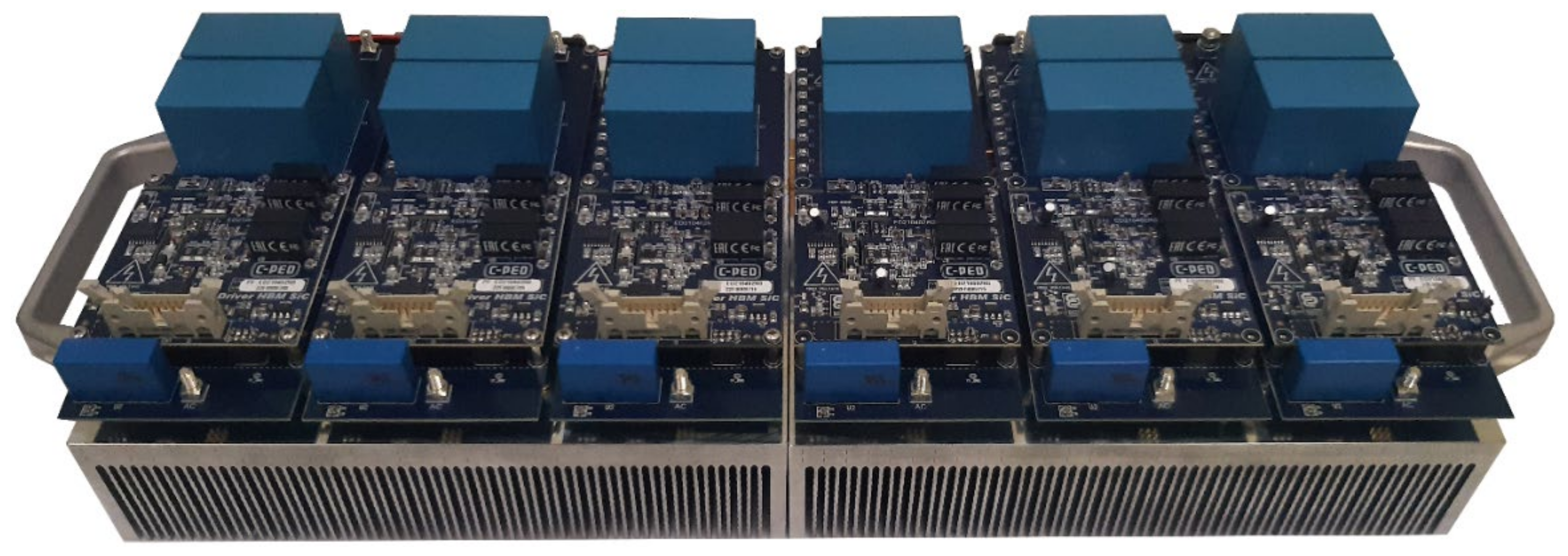
3. Results
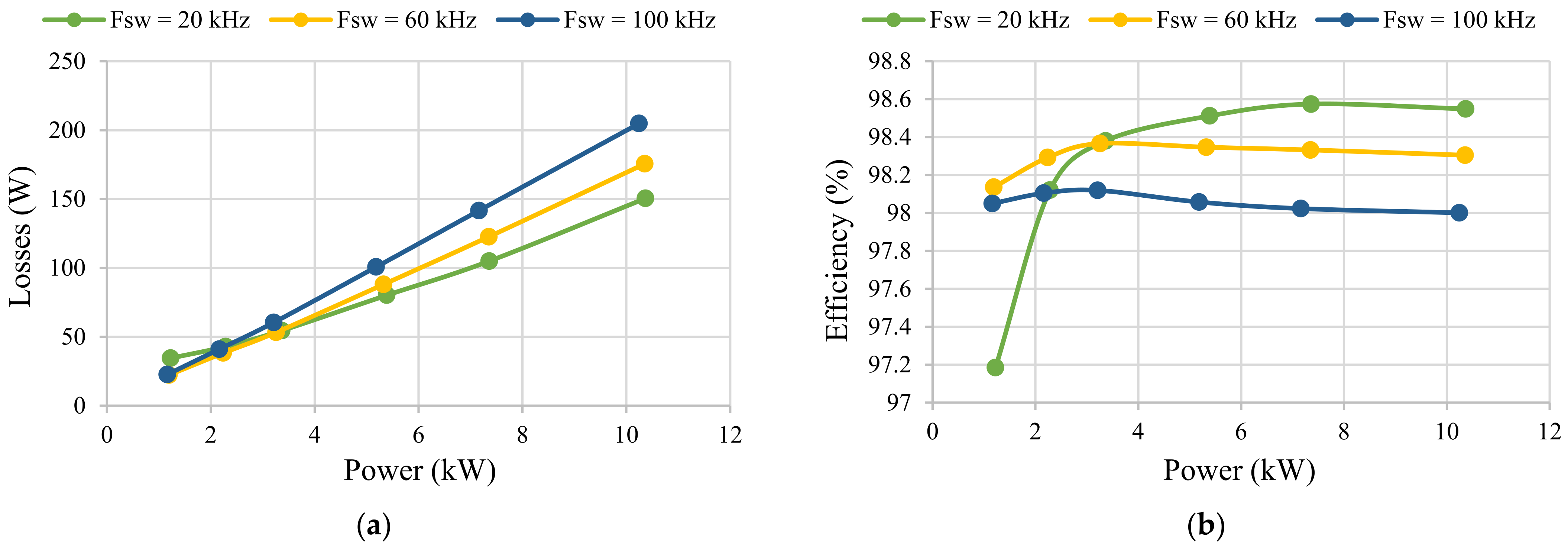
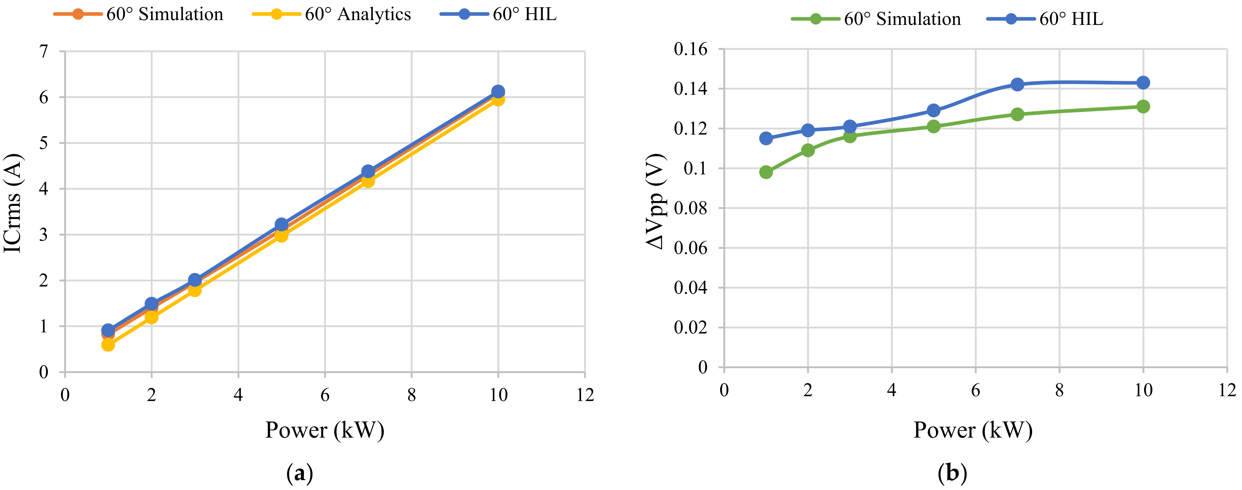
3.1. Simulation Results
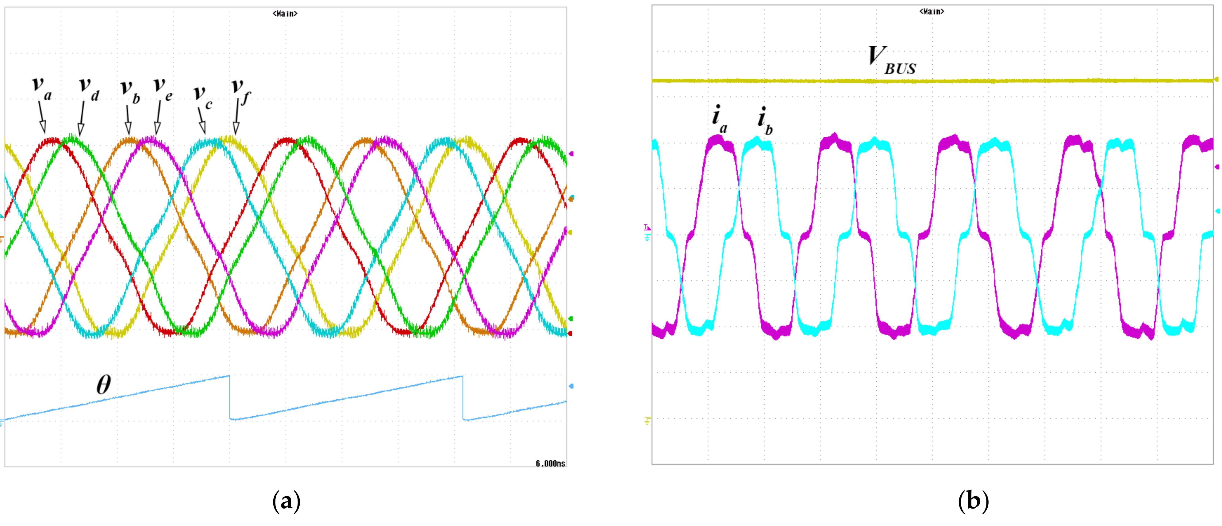
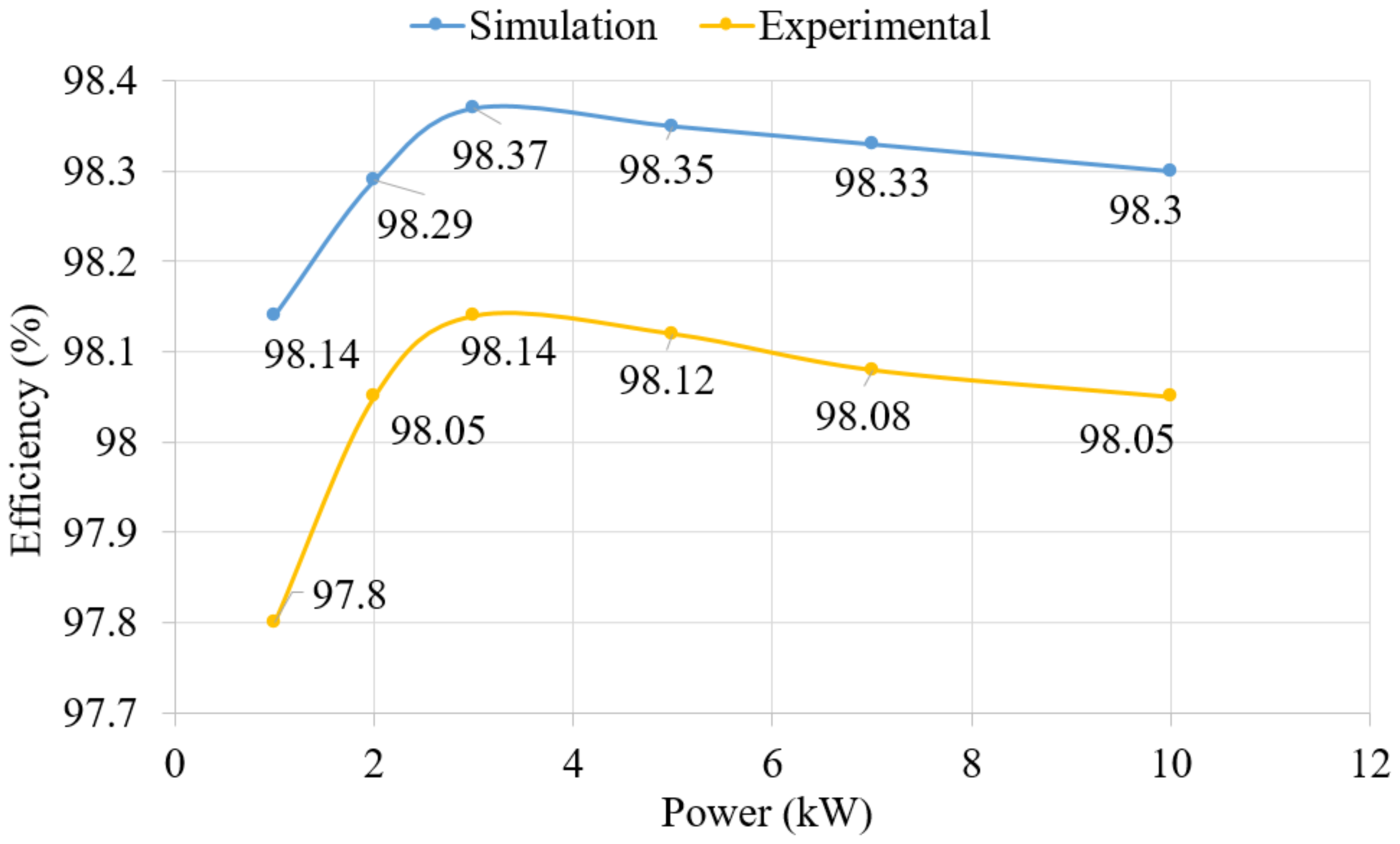
3.2. Experimental Results
4. Conclusions
Author Contributions
Funding
Institutional Review Board Statement
Informed Consent Statement
Data Availability Statement
Acknowledgments
Conflicts of Interest
Correction Statement
References
- Renewables Global Status Report, Renewable Energy Policy Network for the 21st Century (REN21). Available online: https://www.ren21.net/wp-content/uploads/2019/05/GSR2021_Full_Report.pdf (accessed on 31 January 2022).
- Mulongo, N.Y.; Kholopane, P. An economic competitiveness analysis of power generation plants. In Proceedings of the 2018 5th International Conference on Industrial Engineering and Applications (ICIEA), Singapore, 26–28 April 2018; pp. 543–547. [Google Scholar] [CrossRef]
- Tong, K.C. Technical and economic aspects of a floating offshore wind farm. J. Wind. Eng. Ind. Aerodyn. 1998, 74–76, 399–410. [Google Scholar] [CrossRef]
- Manwell, J.F.; Elkinton, C.N.; Rogers, A.L.; McGowan, J.G. Review of design conditions applicable to offshore wind energy systems in the United States. Renew. Sustain. Energy Rev. 2007, 11, 210–234. [Google Scholar] [CrossRef]
- May, T.W.; Yeap, Y.M.; Ukil, A. Comparative evaluation of power loss in HVAC and HVDC transmission systems. In Proceedings of the 2016 IEEE Region 10 Conference (TENCON), Singapore, 22–25 November 2016; pp. 637–641. [Google Scholar] [CrossRef]
- Yaramasu, V.; Wu, B.; Sen, P.C.; Kouro, S.; Narimani, M. High-power wind energy conversion systems: State-of-the-art and emerging technologies. Proc. IEEE 2015, 103, 740–788. [Google Scholar] [CrossRef]
- Yaramasu, V.; Dekka, A.; Durán, M.J.; Kouro, S.; Wu, B. PMSG-based wind energy conversion systems: Survey on power converters and controls. IET Electr. Power Appl. 2017, 11, 956–968. [Google Scholar] [CrossRef]
- Zhu, Z.; Hu, J. Electrical machines and power-electronic systems for high-power wind energy generation applications. COMPEL Int. J. Comput. Math. Electr. Electron. Eng. 2012, 32, 34–71. [Google Scholar] [CrossRef]
- Li, J.; Huang, A.; Bhattacharya, S.; Jing, W. Application of active NPC converter on generator side for MW direct-driven wind turbine. In Proceedings of the 2010 Twenty-Fifth Annual IEEE Applied Power Electronics Conference and Exposition (APEC), Palm Springs, CA, USA, 21–25 February 2010; pp. 1010–1017. [Google Scholar] [CrossRef]
- Boettcher, M.; Fuchs, F.W. Power electronic converters in wind energy systems—Considerations of reliability and strategies for increasing availability. In Proceedings of the 2011 14th European Conference on Power Electronics and Applications, Birmingham, UK, 30 August–1 September 2011; pp. 1–10. [Google Scholar]
- He, J.; Yang, Q.; Wang, Z. On-line fault diagnosis and fault-tolerant operation of modular multilevel converters—A comprehensive review. CES Trans. Electr. Mach. Syst. 2020, 4, 360–372. [Google Scholar] [CrossRef]
- Jlassi, I.; Cardoso, A.J.M. Fault-Tolerant Back-to-Back Converter for Direct-Drive PMSG Wind Turbines Using Direct Torque and Power Control Techniques. IEEE Trans. Power Electron. 2019, 34, 11215–11227. [Google Scholar] [CrossRef]
- Yang, S.; Bryant, A.; Mawby, P.; Xiang, D.; Ran, L.; Tavner, P. An industry-based survey of reliability in power electronic converters. IEEE Trans. Ind. Appl. 2009, 47, 1441–1451. [Google Scholar] [CrossRef]
- Jaiswal, S.; Pahuja, G.L. Effect of reliability of wind power converters in productivity of wind turbine. In Proceedings of the 2014 IEEE 6th India International Conference on Power Electronics (IICPE), Kurukshetra, India, 8–10 December 2014; pp. 1–6. [Google Scholar] [CrossRef]
- Antoszczuk, P.; Retegui, R.G.; Funes, M.; Carrica, D. Optimized Implementation of a Current Control Algorithm for Multiphase Interleaved Power Converters. IEEE Trans. Ind. Inform. 2014, 10, 2224–2232. [Google Scholar] [CrossRef]
- Varzaneh, M.G.; Rajaei, A.; Jolfaei, A.; Khosravi, M. A High Step-up Dual-Source Three Phase Inverter Topology with Decoupled and Reliable Control Algorithm. IEEE Trans. Ind. Appl. 2019, 56, 4501–4509. [Google Scholar] [CrossRef]
- Chivite-Zabalza, J.; Gironés, C.; Cárcar, A.; Larrazabal, I.; Olea, E.; Zabaleta, M. Comparison of power conversion topologies for a multi-megawatt off-shore wind turbine, based on commercial Power Electronic Building Blocks. In Proceedings of the IECON 2013—39th Annual Conference of the IEEE Industrial Electronics Society, Vienna, Austria, 10–13 November 2013; pp. 5242–5247. [Google Scholar] [CrossRef]
- She, X.; Huang, A.Q.; Lucia, O.; Ozpineci, B. Review of Silicon Carbide Power Devices and Their Applications. IEEE Trans. Ind. Electron. 2017, 64, 8193–8205. [Google Scholar] [CrossRef]
- Elasser, A.; Chow, T. Silicon carbide benefits and advantages for power electronics circuits and systems. Proc. IEEE 2002, 90, 969–986. [Google Scholar] [CrossRef]
- Gonzalez, J.O.; Wu, R.; Jahdi, S.; Alatise, O. Performance and Reliability Review of 650 V and 900 V Silicon and SiC Devices: MOSFETs, Cascode JFETs and IGBTs. IEEE Trans. Ind. Electron. 2019, 67, 7375–7385. [Google Scholar] [CrossRef]
- di Nezio, G.; di Benedetto, M.; Lidozzi, A.; Solero, L. Design of a SiC Mosfet 6-Phase Boost Rectifier. In Proceedings of the 2021 21st International Symposium on Power Electronics (Ee), Novi Sad, Serbia, 27–30 October 2021; pp. 1–6. [Google Scholar] [CrossRef]
- Di Benedetto, M.; Lidozzi, A.; Solero, L.; Crescimbini, F.; Grbovic, P.J. Low Volume and Low Weight 3-Phase 5-Level Back to Back E-Type Converter. IEEE Trans. Ind. Appl. 2019, 55, 7377–7388. [Google Scholar] [CrossRef]
- Di Benedetto, M.; Lidozzi, A.; Solero, L.; Crescimbini, F.; Grbović, P. High-Performance 3-Phase 5-Level E-Type Multilevel–Multicell Converters for Microgrids. Energies 2021, 14, 843. [Google Scholar] [CrossRef]
- Kolar, J.; Round, S. Analytical calculation of the RMS current stress on the DC-link capacitor of voltage-PWM converter systems. IEEE Proc. Electr. Power Appl. 2006, 153, 535–543. [Google Scholar] [CrossRef]
- Pei, X.; Zhou, W.; Kang, Y. Analysis and Calculation of DC-Link Current and Voltage Ripples for Three-Phase Inverter with Unbalanced Load. IEEE Trans. Power Electron. 2014, 30, 5401–5412. [Google Scholar] [CrossRef]
- Vujacic, M.; Hammami, M.; Srndovic, M.; Grandi, G. Evaluation of DC voltage ripple in three-phase PWM voltage source inverters. In Proceedings of the 2017 IEEE 26th International Symposium on Industrial Electronics (ISIE), Edinburgh, UK, 19–21 June 2017; pp. 711–716. [Google Scholar] [CrossRef]


| Phase Displacement δ | Voltage Ripple Δvpp | Normalized Current Stress ICrms/Im |
|---|---|---|
| 0° | 0.92 | |
| 30° | 0.87 | |
| 60° | 0.83 |
Publisher’s Note: MDPI stays neutral with regard to jurisdictional claims in published maps and institutional affiliations. |
© 2022 by the authors. Licensee MDPI, Basel, Switzerland. This article is an open access article distributed under the terms and conditions of the Creative Commons Attribution (CC BY) license (https://creativecommons.org/licenses/by/4.0/).
Share and Cite
Di Nezio, G.; di Benedetto, M.; Lidozzi, A.; Solero, L. Analysis and Design of a High-Efficiency SiC MOSFET 6-Phase Boost Rectifier. Energies 2022, 15, 2175. https://doi.org/10.3390/en15062175
Di Nezio G, di Benedetto M, Lidozzi A, Solero L. Analysis and Design of a High-Efficiency SiC MOSFET 6-Phase Boost Rectifier. Energies. 2022; 15(6):2175. https://doi.org/10.3390/en15062175
Chicago/Turabian StyleDi Nezio, Giulia, Marco di Benedetto, Alessandro Lidozzi, and Luca Solero. 2022. "Analysis and Design of a High-Efficiency SiC MOSFET 6-Phase Boost Rectifier" Energies 15, no. 6: 2175. https://doi.org/10.3390/en15062175
APA StyleDi Nezio, G., di Benedetto, M., Lidozzi, A., & Solero, L. (2022). Analysis and Design of a High-Efficiency SiC MOSFET 6-Phase Boost Rectifier. Energies, 15(6), 2175. https://doi.org/10.3390/en15062175