Article

Analysis of Circuit Parameters of New Graphene Partial Discharge Sensor Electrode Plate Based on Transmission Line Model

School of Electrical Engineering, Beijing Jiaotong University, Beijing 100044, China
*
Author to whom correspondence should be addressed.
Energies 2022, 15(6), 2169; https://doi.org/10.3390/en15062169
Submission received: 25 January 2022 / Revised: 7 March 2022 / Accepted: 14 March 2022 / Published: 16 March 2022

Abstract

:
Partial discharge (PD) sensors have been widely used in PD detection of power equipment. In order to adapt to the development of the new power system, the new PD sensor should not only have a wide response band but also have a large dynamic range. PD measurement devices currently used in smart grids are mainly based on traditional metal materials, which face difficulty in fully meeting these technical requirements. Graphene has a variety of excellent properties, and it is introduced to improve PD sensor materials in this paper. Based on the transmission line model, the circuit parameters of graphene PD sensor electrode plate material are theoretically derived. Various factors affecting its resistance characteristics, inductance characteristics, and capacitance characteristics are analyzed. Next, the variation curves of circuit parameters under different influencing factors are obtained. Linear regression models based on the least-square method were developed for circuit parameters. Finally, the simulation and experiment verified that the graphene PD sensor has high gain characteristics. The simulation results are consistent with the experimental results, further verifying the feasibility of the circuit parameter study. This study can be used to guide the design of the new graphene PD sensors.

1. Introduction

High-voltage switchgear is widely used in power systems, and the insulation condition of switchgear is directly related to the reliability and safety of the power system [1,2,3]. Due to uneven insulating medium or the presence of bubbles, partial discharges often occur internally in operating electrical equipment, which will accelerate insulation degradation and leads to equipment operational failures [4]. According to the statistical data of switchgear operation accidents, insulation faults account for 31.9% of the total number of accidents and tops the list of accidents [5]. With the increasing scale of the power grid and the increasing requirement of power supply reliability, the state maintenance of switchgear has become a trend [6]. The important content of the state maintenance of power equipment is the detection of insulation state. Meanwhile, partial discharge is the main factor of equipment insulation aging and is the main reason for insulation faults [7]. Therefore, it is necessary to detect the partial discharge of switchgear accurately.
At present, the existing methods for partial discharge detection of switchgear equipment mainly include ultra-high frequency method [8], ultrasonic method [9,10], radiofrequency method [11], pulse current method [12,13,14], and transient earth voltage (TEV) method [15]. UHF partial discharge detection technique uses antenna sensors for detection, with a wide frequency band and high interference immunity [16]. The advantage of the ultrasonic detection method is that it can detect online and is not subject to industrial frequency interference. However, the sensitivity of this detection method is low, which is generally not used as a switchgear detection method [17]. The RF detection method uses RF sensors to detect the electromagnetic wave signal generated by partial discharge. However, it is necessary to cooperate with the use of capacitive, coil current, or RF antenna sensors when applied [11]. The pulse current method is applicable under both AC and DC conditions and is widely used [12]. In [18,19], the feasibility of using the TEV method for the identification of PD was proved. This method can perform online detection on operating equipment and has high sensitivity. Among them, the TEV method has the advantages of high sensitivity, non-invasion, and simple use. Thus, it is gradually being promoted and applied in the insulation condition detection of switchgear. However, the traditional TEV sensor has a simple structure, narrow frequency band, and poor coupling of discharge signal, which has difficulty in meeting the development needs of the new power system. Due to the traditional TEV sensor whose electrode plate is a copper sheet, the coupling performance of the partial discharge signal is greatly limited. Additionally, the optimization capability is limited, without considering the improvement of the material properties of the electrode plates.
As a new type of electronic material, graphene has a special energy band structure The properties of graphene at room temperature are shown in Table 1.
That is to say, the carrier mobility of graphene is 6000 times that of copper. The resistivity of graphene is the smallest known resistivity. Graphene is the best conductive material at room temperature today. Considering the excellent electrical properties of graphene material, the introduction of graphene aims to improve the coupling performance and enhance the transmission capability of the PD signal.
Graphene has been developed and applied in many fields such as nanomaterials, biology, electronic and information engineering, and chemistry. By micro-regulating graphene, more sensing materials can be explored, with excellent electrical properties. This material has a strong competitive ability compared to traditional sensing materials. In the field of sensors, in [20], a flexible Hall sensor based on graphene material was developed. The sensitivity is comparable to that of Hall sensors made of traditional semiconductor materials. In [21], Friedman tested the magnetoresistive properties of concentric graphene electromagnetic resistive sensing elements, which were prepared by vapor-phase deposition. Ref. [22] proposed the concept of graphene reconfigurable antennas for applications in the terahertz (THz) band. Ref. [23] analyzed the potential applications of graphene in the microwave band for reconfigurable antennas. In [24], the concept of a graphene-based two-dimensional leaky-wave antenna (LWA) was proposed, which can enable frequency tuning and beam control in the terahertz band. However, the application of graphene materials has not been seen in the field of PD measurement.
Regarding the study of the circuit parameter of graphene PD sensor, the electrothermal characterization of multilayer copper-graphene heterogeneous interconnects was analyzed under electrostatic discharge (ESD) [25]. In [26], a high-frequency model was performed on copper-graphene interconnects, which theoretically investigates the transmission characteristics at high frequencies. In [27], an analytical model of the effective resistance of a two-dimensional resistive network was developed and applied to multilayer graphene nanoribbon interconnects. The above references have studied copper and graphene interconnections, but the material parameter characteristics for graphene copper-clad electrode plates have not been reported.
Transmission line theory can be used to analyze the distribution of voltage and current, as well as the rules of impedance on the transmission line. Therefore, this paper proposes the study of circuit parameters of new graphene PD sensor electrode plate material based on the transmission line model. The resistance characteristics, inductance characteristics, and capacitance characteristics of graphene partial discharge were studied theoretically. We also analyze the effects of Fermi energy level, width, thickness, and the number of layers on the circuit parameters of the electrode plate. Circuit parameter prediction models were developed based on the least-square method. This paper focuses on circuit parameters study for graphene partial discharge sensors. In order to verify the results of the theoretical derivation of the circuit parameters, the frequency characteristics were simulated by the circuit parameters. The purpose of the frequency-domain characteristics experiments is to verify that the frequency characteristics of the experiment are consistent with those of simulation. Thus, the feasibility of the circuit parameter study can be verified. The time-domain characteristics were also analyzed in the experiment. Finally, in order to further test the sensing ability of the graphene sensor on the partial discharge, the switchgear partial discharge detection system was built. This work can lay the foundation for further design of graphene PD sensors.
The rest of the paper is organized as follows. In Section 2, we address some circuit parameters including graphene and copper, respectively. Section 3 proposes a method to analyze the circuit parameters of graphene copper-clad electrode plates considering the coupling. Then, we provide a theoretical qualitative analysis of the influencing factors about circuit parameters in Section 4. Next, a quantitative analysis of each influencing factor is conducted to evaluate our circuit parameters of graphene copper-clad electrode plates in Section 5. Section 6 develops and validates circuit parameter prediction models based on the least-square method. In Section 7, the characteristics of the graphene PD sensor are compared with that of the traditional PD sensor by simulation and experimental analysis. Finally, we conclude our work in Section 8.

2. Circuit Parameters

When partial discharge occurs in the electrical equipment inside the switchgear, high-frequency electromagnetic waves will be generated. The electromagnetic wave will lead to refraction and reflection in the electrical equipment or conductors. Therefore, the surface of the switchgear will generate changing electric and magnetic fields. At the same time, the changing electric and magnetic fields will generate current and a transient earth voltage on the surface of the switchgear [28].
The TEV sensor can detect this voltage and its detection principle is shown in Figure 1.
Where u is the transient earth wave, C1 is the equivalent capacitance between the up-plate of the TEV sensor and the surface of the switchgear shell, C2 is the internal capacitance of the TEV sensor, Rosc is the impedance of the oscilloscope, and U2 is the value of the induced voltage on the TEV sensor.
The traditional TEV sensor mainly applies the principle of voltage-divider capacitor. By measuring the value of u, it is possible to calculate the voltage on the surface of the switchgear:
U 2 = C 1 C 1 + C 2 u
Traditional improvements for TEV sensors have focused on improving the filling substance of the capacitor, using the following Equation [29]:
C = ε S d .
This method only focuses on the dielectric properties between capacitors, the area of electrode plates, and the distance between the two plates. The optimization capability is limited without considering the improvement of the material properties of the electrode plates. The traditional electrode plate material is copper, its resistivity is 1.72 Ω/cm. However, the resistivity of graphene is 10−6 Ω/cm. It can be seen that the transmission capacity of graphene is much higher than that of the copper electrode plate. Replacing the copper electrode plate with the graphene copper-clad electrode plate can enhance the transmission of electrical signals in partial discharge sensors. Therefore, it is proposed to develop new graphene copper-clad electrode plate material for TEV sensors, which is based on the original copper electrode plate. The transmission line model can analyze the transmission characteristics of PD sensors. For this purpose, based on the transmission line model, this paper analyzes the circuit parameter characteristics for the electrode plate material, mainly considering the resistance characteristics, capacitance characteristics, and inductance characteristics.

2.1. Resistive Properties of Graphene

The resistance of graphene can be equated to three parts: quantum resistance Rq, contact resistance Rc, and scattering resistance Rs. Additionally, the total resistance can be viewed as a series connection of these three resistances. The graphene used to study as PD sensor electrode plate material is metallic armchair graphene. Therefore, the next parameters are studied according to metallic armchair graphene. The resistance of graphene increases with length. The expressions can be obtained as:
R = R q + R c + R s = l r q + r c + r s

2.1.1. Quantum Resistance

The quantum effect leads to quantum resistance. Nch is used to denote the number of conducting channels in the graphene. Additionally, since the electron spin is 2, it is equivalent to 2Nch electron transport channels. The expression of quantum resistance per unit length can be expressed as [30]:
r q = h 2 e 2 N ch 12.9 N ch
The number of conduction channels of the metallic armchair graphene grows almost linearly when the width is greater than 10 nm. To reduce the calculation, Nch can be simplified in the approximate allowed range. The widths of graphene studied in this paper are all taken to be above 10 nm. Additionally, the Nch of graphene in this width range can be expressed as a linear approximation [31]:
N ch = α E F W
where W is the width in nm, α is the operation parameter and the approximate value is 1.2 (eV·nm)−1.

2.1.2. Contact Resistance

The contact resistance of a single layer or several layers of graphene is at most a few hundred ohms, which is small compared to the quantum resistance. Therefore, contact resistance is generally neglected during the research process, especially during qualitative studies.

2.1.3. Scattering Resistance

The scattering resistance per unit length of single-layer graphene can be obtained as [32]
r s = r q λ eff = h 2 e 2 N ch λ eff
λ eff = W 1 P g r 2 W E F ih v F 2 1
where the unit of rq and rs is kΩ/μm, λeff is the effective mean free path of the electrons in each channel of graphene.

2.2. Inductive Properties of Graphene

The inductance of graphene consists of two parts: the magnetoelectric inductance lm and the dynamic inductance lk. The total inductance is the series of the two parts. Both magnetoelectric inductance and dynamic inductance increase with length, which are distributed parameters. The expressions can be obtained as:
L = L m + L k = l l m + l k

2.2.1. Magnetoelectric Inductance

The current flowing through the conductor generates a magnetic field around the conductor, which can be equivalent to an inductance storing the same amount of energy, called magnetoelectric inductance lm. The equivalent magnetoelectric inductance per unit length of single-layer graphene can be calculated as [32].
l m = μ 0 2 π cosh 1 π d / W = μ d / W

2.2.2. Dynamic Inductance

In graphene, the kinetic energy of the electrons is very high. It can be equated to the energy stored in an inductor [33], which is called dynamic inductor lk. Therefore, the dynamic inductance per unit length of single-layer graphene can be expressed as [34]
l k = h 4 e 2 v F N ch 8 N ch
where the unit of lk and lm is nH/μm.

2.3. Capacitive Properties of Graphene

The capacitance of graphene consists of two parts, electrostatic capacitance Ce and quantum capacitance Cq. The total capacitance is a series connection of the two parts.
C = C e 1 + C q 1 1

2.3.1. Electrostatic Capacitance

When the voltage is applied to a conductor, it will naturally generate an electrostatic field, which can be equivalent to electrostatic capacitance ce. The equivalent electrostatic capacitance per unit length of single-layer graphene can be expressed as
c e = ε 0 W / d

2.3.2. Quantum Capacitance

When electrons are added to the graphene, the energy of the electrons must reach the energy of the lowest unoccupied energy level above EF. Additionally, the increased potential energy can be equivalent to the energy stored in a capacitor, called quantum capacitance cq. The quantum capacitance per unit length of single-layer graphene can be expressed as [34]
c q = 4 e 2 N ch h v F = 200 N ch
where the unit of ce and cq is aF/μm.

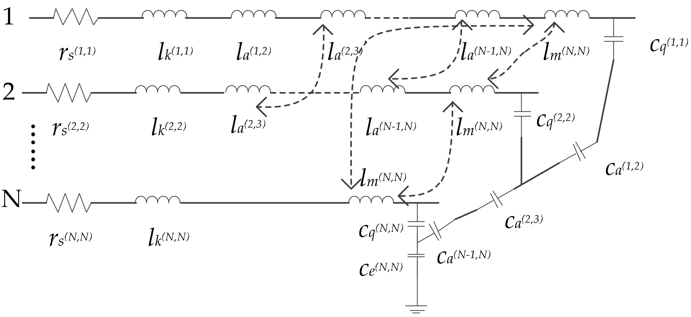
2.4. Circuit Parameters of Multilayer Graphene

Section 2.1, Section 2.2 and Section 2.3 are mainly for single-layer graphene. Multilayer graphene can be regarded as a stack of single layers of graphene, and every single layer of graphene is connected in parallel with each other. The difference between multilayer graphene and single-layer graphene is the mutual coupling between layers. Thus, the mutual capacitance and mutual inductance between layers should be taken into consideration.
The equivalent model of multilayer graphene is shown in the following Figure 2.
Where, 1-N represents the number of graphene layers, rs(N,N) represents the scattering resistance of each layer, lk(N,N) represents the kinetic inductance of each layer, la(N−1,N) represents the mutual inductance, lm(N,N) represents the magnetoelectric inductance, cq(N,N) represents the quantum capacitance, ca(N−1,N) represents the mutual capacitance, and ce(N,N) represents the electrostatic capacitance. It can be seen that the resistance between each layer shows a parallel relationship, and both capacitance and inductance are coupled.

2.4.1. Mutual Inductance

The mutual inductance in multilayer graphene acts on the single-layer kinetic inductance, which in turn affects the multilayer graphene kinetic inductance. The mutual inductance between adjacent layers of N-layer graphene per unit length can be given as [35]
l a = μ δ / W
The dynamic inductance of a single layer in N-layer graphene lk is shown in Equation (10). According to Figure 2, by analyzing the series-parallel connection between mutual inductance la, magneto-inductance lm, and dynamic inductance lk, we can calculate the dynamic inductance li per unit length of N-layer graphene using the iterative method:
l 1 = l k ( 1 , 1 ) 1 l i = 1 l k ( i , i ) + 1 l i 1 + l a ( i 1 , i ) i 2 , N
where i represents the number of graphene layers.

2.4.2. Mutual Capacitance

Coupling capacitance exists between the layers of multilayer graphene. The interlayer coupling mutual capacitance in multilayer graphene acts on the single-layer quantum capacitance, which in turn affects the multilayer graphene quantum capacitance step by step. The interlayer coupling mutual capacitance per unit length of N-layer graphene can be expressed as
c m = ε W / δ
The electrostatic capacitance of N-layer graphene cq is given by Equation (13). According to Figure 2, by analyzing the series-parallel connection between the electrostatic capacitance ce, the quantum capacitance cq, and the mutual capacitance between adjacent layers ca, we can calculate the quantum capacitance ci per unit length of the N-layer graphene by iterating:
c 1 = c q ( 1 , 1 ) c i = c q ( i , i ) + 1 c i 1 + 1 c m ( i 1 , i ) 1 i 2 , N
where i represents the number of graphene layers.

2.5. Characteristics of Copper

As a metallic conductor, the only circuit parameter of copper is resistance. For each copper cell, the bulk resistivity of copper ρ0 is 1.7 μΩ·cm. The mean free path of copper λcu is 37.3 nm. The average boundary spacing dg is equal to the width w. The specular reflection coefficient of copper is Pcu = 0.41. Scattering coefficient is R = 0.22 [33].

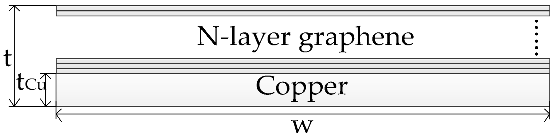
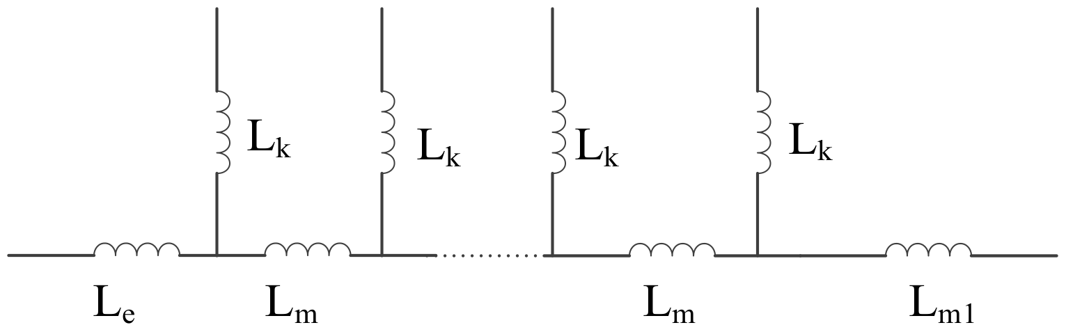
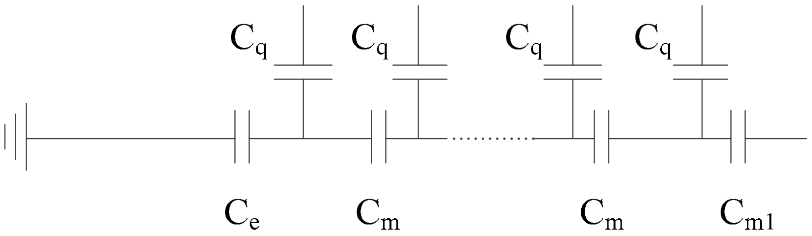
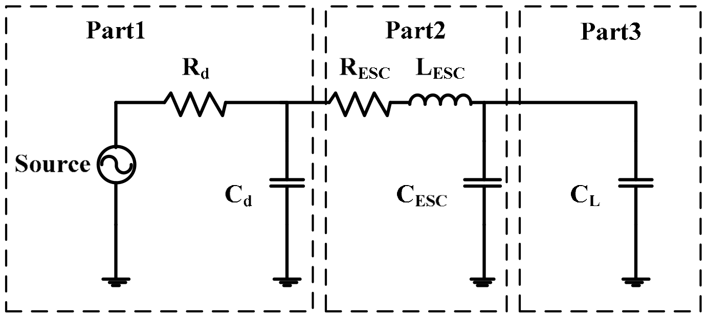
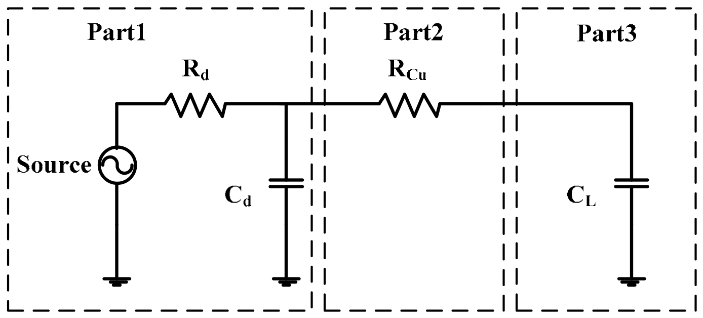
3. Circuit Parameters of Graphene Copper-Clad Electrode Plates

Figure 3 shows the graphene copper-clad electrode plate model. In this figure, t represents the total thickness of the electrode plate, tCu is the thickness of copper, and w is the total width. This figure shows the electrode plate profile. It can be seen that the electrode plate has N-layer graphene in the upper part and copper in the lower part.
Graphene needs to be attached to copper plates. Additionally, the coupling between copper and graphene will affect the characteristics whole electrode plate. It is necessary to analyze the parametric characteristics of the graphene copper-clad structure.

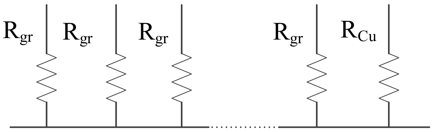
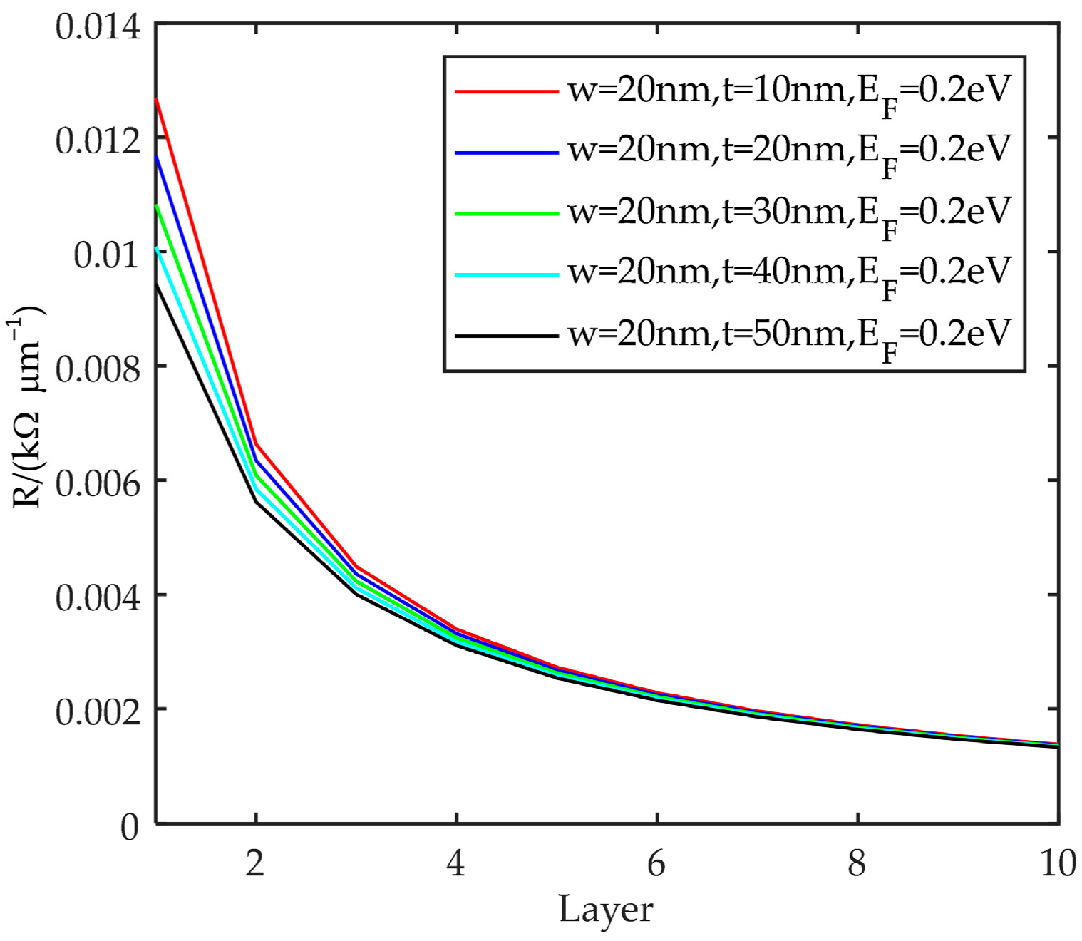
3.1. Resistance Characteristics

Figure 4 shows that copper and graphene can be viewed as parallel structures in graphene copper-clad electrode plate. The resistance between multiple layers of graphene is in parallel as well. Rgr represents the resistance of single-layer graphene. RCu represents the resistance of copper. The equivalent resistance can be expressed as
R ESC = 1 R Cu + N 1 R gr 1
where, as for Rgr, the specular parameter of graphene Pgr is taken to be 0. Rgr can be approximated by
R gr = h 2 e 2 1 N ch 1 λ Cu + 1 λ eff

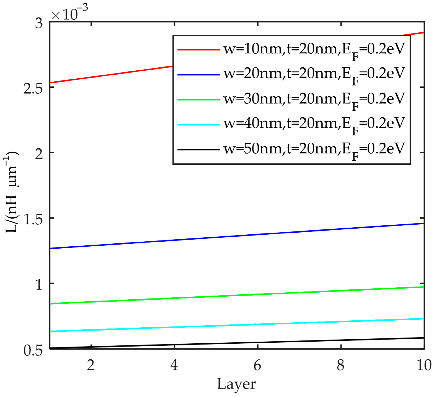
3.2. Inductance Characteristics

The inductance circuit diagram of the graphene copper-clad electrode plate can be shown as follows.
Figure 5 shows the relationship of inductance in graphene copper cladding. Among them, Le represents graphene magnetoelectric inductance, Lk represents the kinetic inductance of graphene layers, Lm represents magnetic mutual inductance between adjacent graphene layers, Lm1 represents magnetic mutual inductance between Cu and graphene layers. These parameters can be obtained as:
L e = μ 0 t / w L k = 8 / N ch L m = μ 0 δ / w L m 1 = μ 0 δ 1 / w Cu
where the distance between Cu and graphene layers δ1 is taken as 0.155 nm [30].
Assuming that the copper and graphene layers are at the same potential, Lrec can be obtained by iteration:
L rec = L rec N L rec 1 = 1 L m 1 + 1 L k 1 L rec i = 1 L rec i 1 + L m + 1 L k 1   ,   i 2 , N
The equivalent inductance of graphene copper cladding is
L ESC = L rec + L e

3.3. Capacitance Characteristics

The capacitance circuit diagram of graphene copper cladding can be shown as follows.
Figure 6 shows the relationship of capacitance in graphene copper cladding. Ce represents electrostatic capacitance, Cq represents the quantum capacitance of graphene layers, and Cm represents the electrostatic mutual capacitance between adjacent graphene layers. Cm1 represents the electrostatic mutual capacitance between copper and graphene layers. These parameters can be obtained as:
C e = ε 0 W / d C q = 200 N ch C m = ε 0 w / δ C m 1 = ε 0 w Cu / δ 1
Assuming that the copper and graphene layers are at the same potential, Crec can be obtained by iteration:
C rec = C rec N C rec 1 = C m 1 + C q C rec i = 1 C rec i 1 + 1 C m 1 + C q   ,   i 2 , N
The equivalent capacitance of graphene copper cladding is
C ESC = 1 C rec + 1 C e 1

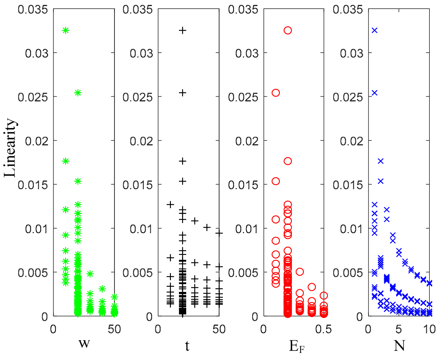
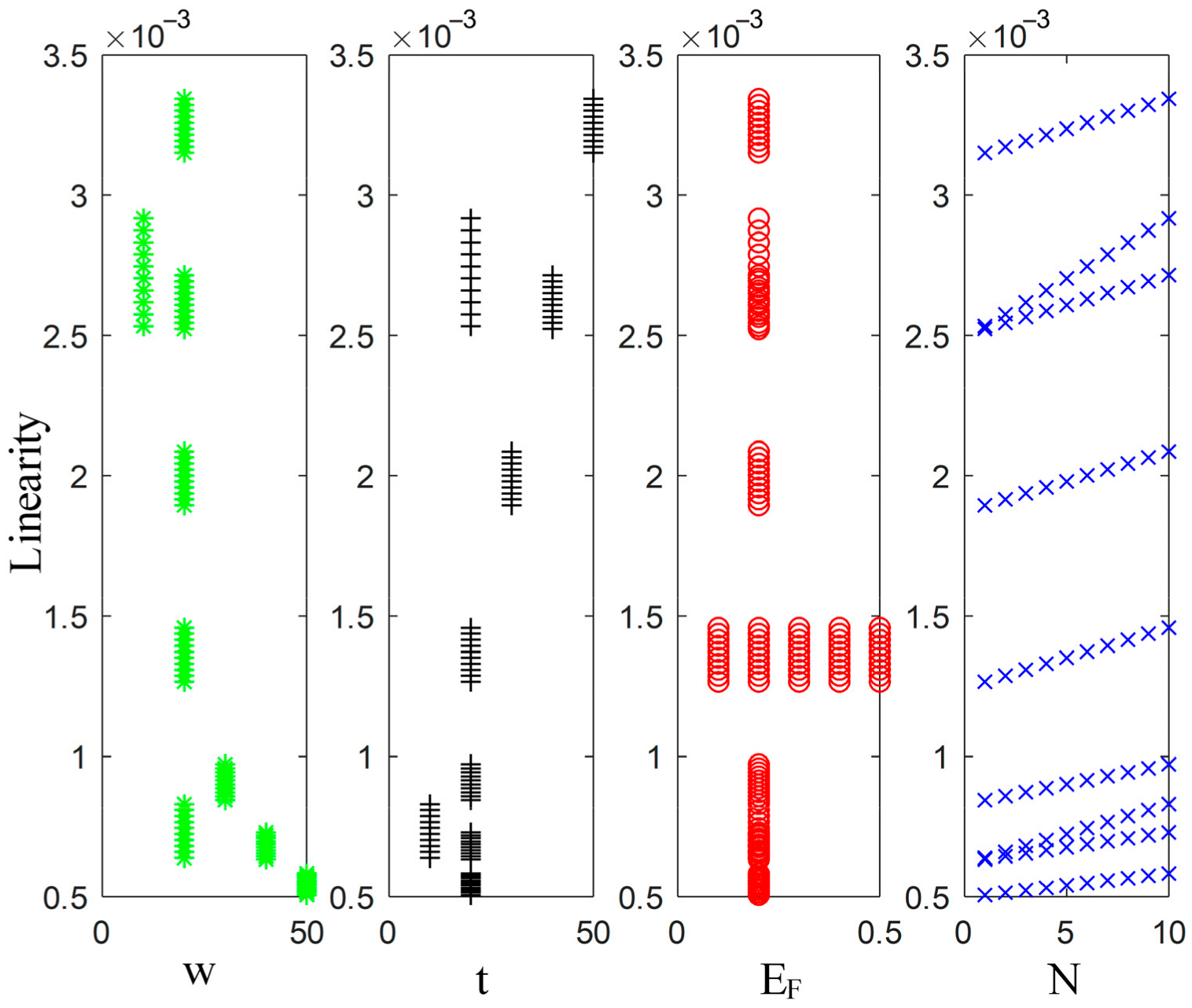
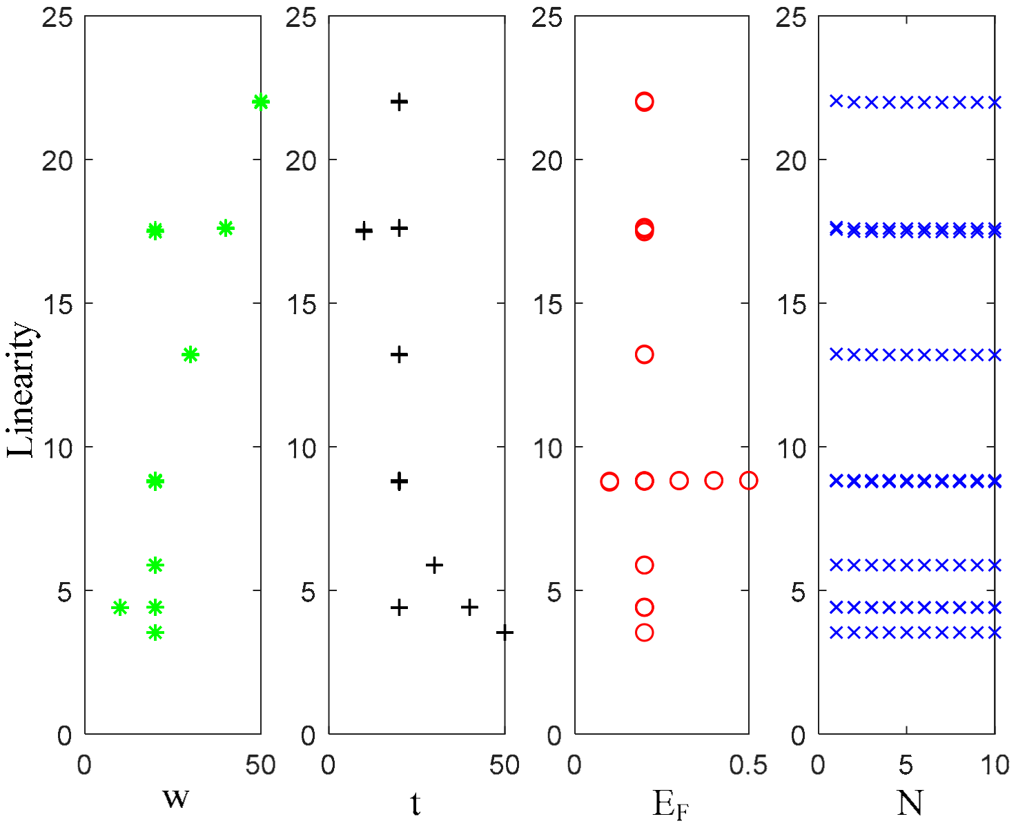
4. Analysis of Influencing Factors

This section provides a theoretical qualitative analysis of the influencing factors about circuit parameters, such as width, thickness, Fermi energy level, and the number of layers. The next calculation section will provide a quantitative analysis of each influencing factor.

4.1. Width

In the electrode plate material, the width of graphene is the same as that of copper.
As for the resistance characteristics, the width not only changes the copper resistance but also causes the graphene conducting channel Nch to change. Nch in turn affects the mean free path, altering the graphene resistance. Ultimately, the overall equivalent resistance will change.
As for the inductance characteristics, the width will affect the magnetic inductance, the inductance between copper and graphene, and the coupling mutual inductance between graphene layers. Meanwhile, due to the change in the number of Nch, the dynamic inductance will change. Eventually, these changes will have an impact on the overall equivalent inductance.
As for the capacitance characteristics, the width will cause a change in electrostatic capacitance, capacitance between copper and graphene, and mutual capacitance between graphene layers. Meanwhile, due to the change in the number of Nch, the quantum capacitance of graphene will change. Lastly, the overall equivalent capacitance will be altered.

4.2. Thickness and Number of Layers

Thickness refers to the total thickness t, which is divided into two components, the thickness of copper and the thickness of graphene, respectively. The thickness of copper will affect the equivalent resistivity of copper. However, the thickness of graphene will determine the specific number of graphene layers. It is known that the distance between adjacent graphene layers is δ = 0.34 nm, which is called the van der Waals distance. Thus, the number of multilayer graphene layers can be expressed as [33]
N = I n t e r t Gr / δ + 1
In terms of resistance characteristics, once the thickness of copper changes, the equivalent resistivity of copper will change. In this way, the copper resistance will be affected. At the same time, the number of layers will lead to a change in the number of parallel graphene resistances, Finally, it will lead to the change of equivalent resistance.
In terms of inductance characteristics, firstly, the total thickness variation will affect the magneto-inductance. Then, the number of layers changes the magnetic mutual inductance between graphene, which eventually leads to the change of equivalent inductance.
In terms of capacitance characteristics, the total thickness variation will affect the electrostatic capacitance. Then, the number of layers will change the electrostatic mutual capacitance between graphene. Eventually, the equivalent capacitance will be changed.

4.3. Fermi Energy Level

The changes in the Fermi energy level will affect the number of conducting channels of graphene Nch.
As for resistance characteristics, the change of the number of Nch directly affects the total mean free path. It will in turn change the graphene resistance. Ultimately the overall equivalent resistance will be changed.
As for inductance characteristics, the change of the number of Nch directly affects the kinetic inductance, which in turn affects the magnetic mutual inductance through iteration. Eventually, the overall equivalent inductance will be changed.
As for capacitive characteristics, the number of Nch directly affects the quantum capacitance, which in turn affects the electrostatic mutual capacitance through iteration. Finally, the overall equivalent capacitance will be changed.

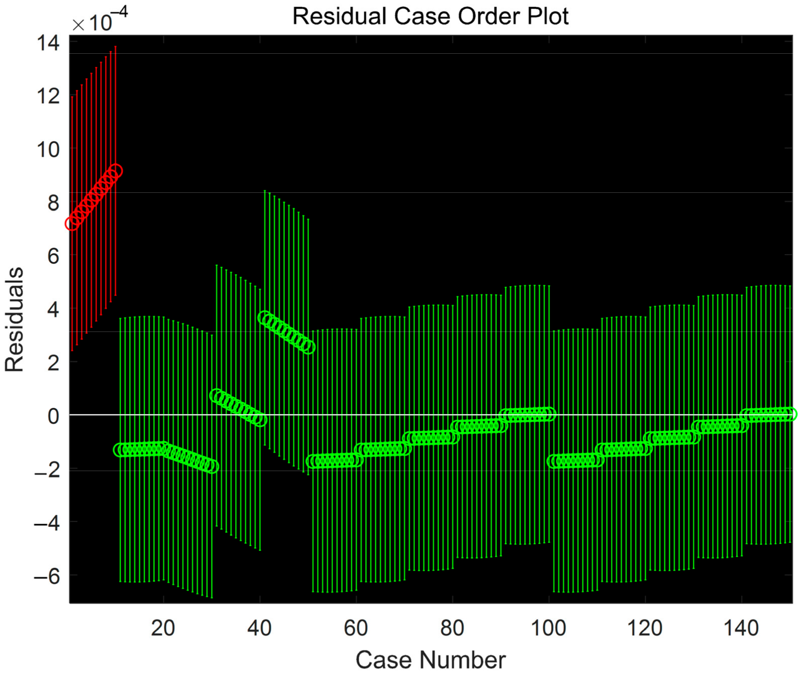
5. Computational Analysis

In this part, the resistance, capacitance, and inductance of multilayer graphene copper-clad electrode plate material are calculated by MATLAB under different influencing factors. Additionally, the curve of circuit parameters with the number of layers is derived, when the values of width taken as 10 nm, 20 nm, 30 nm, 40 nm, and 50 nm, total thickness t taken as 10 nm, 20 nm, 30 nm, 40 nm, and 50 nm, and the Fermi energy level EF taken as 0.1 eV, 0.2 eV, 0.3 eV, 0.4 eV, and 0.5 eV, respectively.

5.1. Resistance Characteristics

Fixing the total thickness of 20 nm and the Fermi energy level of 0.2 eV, we analyze the variation of the resistance of the electrode plate with the number of layers when the width is taken as 10 nm, 20 nm, 30 nm, 40 nm, and 50 nm. The curve can be obtained in Figure 7.
In terms of resistance characteristics, the resistance of graphene copper-clad electrode plate material gradually decreases with the increasing number of layers. The reason is that the increasing number of layers corresponds to more resistances in parallel. It leads to the decrease of the overall equivalent resistance. However, the effect of layers number on the resistance tends to stabilize after 6 layers. At the same time, it can be seen that when the width increases, the equivalent resistance tends to decrease.
With the fixed width of 20 nm and the Fermi energy level of 0.2 eV, we analyze the variation of the resistance of the electrode plate with layers number when the total thickness is taken as 10 nm, 20 nm, 30 nm, 40 nm, and 50 nm, respectively. The curve is as shown in the following figure.
Figure 8 shows that the larger the number of layers, the smaller the equivalent resistance. However, when the number of layers is small, the change in total thickness has a relatively large effect on the resistance. Additionally, when the number of layers is greater than or equal to 6, the effect of total thickness on the resistance is negligible.
With a fixed width of 20 nm and a fixed total thickness of 20 nm, we analyze the variation of the resistance of the electrode plate with the number of layers when the Fermi energy level EF is taken as 0.1 eV, 0.2 eV, 0.3 eV, 0.4 eV, and 0.5 eV, respectively. The curve is as shown in the following figure.
Figure 9 shows that the increase of the Fermi energy level causes a gradual decrease of the equivalent resistance.

5.2. Inductance Characteristics

With a fixed total thickness of 20 nm and a Fermi energy level of 0.2 eV, we analyze the variation of the inductance of the electrode plate with the number of layers when the width is taken as 10 nm, 20 nm, 30 nm, 40 nm, and 50 nm, respectively. The curve is as shown in Figure 10.
In terms of inductance characteristics, an increase in the number of layers results in a gentle increase of the equivalent inductance. Meanwhile, the larger the width, the smaller the total inductance of the electrode plate.
With a fixed width of 20 nm and a Fermi energy level of 0.2 eV, we analyze the variation of the inductance of the electrode plate with the number of layers when the total thickness is taken as 10 nm, 20 nm, 30 nm, 40 nm, and 50 nm, respectively. The curve is as shown in the following figure.
Figure 11 shows that the thickness has the opposite effect on the equivalent inductance of the electrode plate as the width.
With a fixed width of 20 nm and a fixed total thickness of 20 nm, we analyze the variation of the inductance of the electrode plate with the number of layers when the Fermi energy level EF is taken as 0.1 eV, 0.2 eV, 0.3 eV, 0.4 eV, and 0.5 eV, respectively. The curve is as shown below.
Figure 12 shows that the change of Fermi energy level does not change the equivalent inductance compared to the effect caused by the width and thickness.

5.3. Capacitance Characteristics

With a fixed total thickness of 20 nm and a Fermi energy level of 0.2 eV, we analyze the variation of the capacitance of the electrode plate with the number of layers when the width is taken as 10 nm, 20 nm, 30 nm, 40 nm, and 50 nm, respectively. The curve is shown in Figure 13.
As for the capacitance characteristics, the equivalent capacitance gradually decreases with the increase of the number of layers. The trend is relatively flat. However, the capacitance tends to increase with the increase of the width.
With a fixed width of 20 nm and a Fermi energy level of 0.2 eV, we analyze the variation of the capacitance of the electrode plate with the number of layers when the total thickness is taken as 10 nm, 20 nm, 30 nm, 40 nm, and 50 nm, respectively. It is as shown in the following figure.
Figure 14 shows that the effect of thickness on capacitance is exactly the opposite of the effect caused by the width of the capacitance. It gradually decreases as the increase of thickness.
With a fixed width of 20 nm and a fixed total thickness of 20 nm, we analyze the variation of the capacitance of the electrode plate with the number of layers when the Fermi energy level EF is taken as 0.1 eV, 0.2 eV, 0.3 eV, 0.4 eV, and 0.5 eV, respectively. The curve is plotted as shown in Figure 15.
The effect of Fermi energy level on the capacitance is relatively small. However, in general, the equivalent capacitance tends to increase as the Fermi energy level becomes larger.
In summary, according to Figure 7, Figure 8, Figure 9, Figure 10, Figure 11, Figure 12, Figure 13, Figure 14 and Figure 15, the relationship between circuit parameters and four influencing factors can be summarized as shown in Table 2 below.

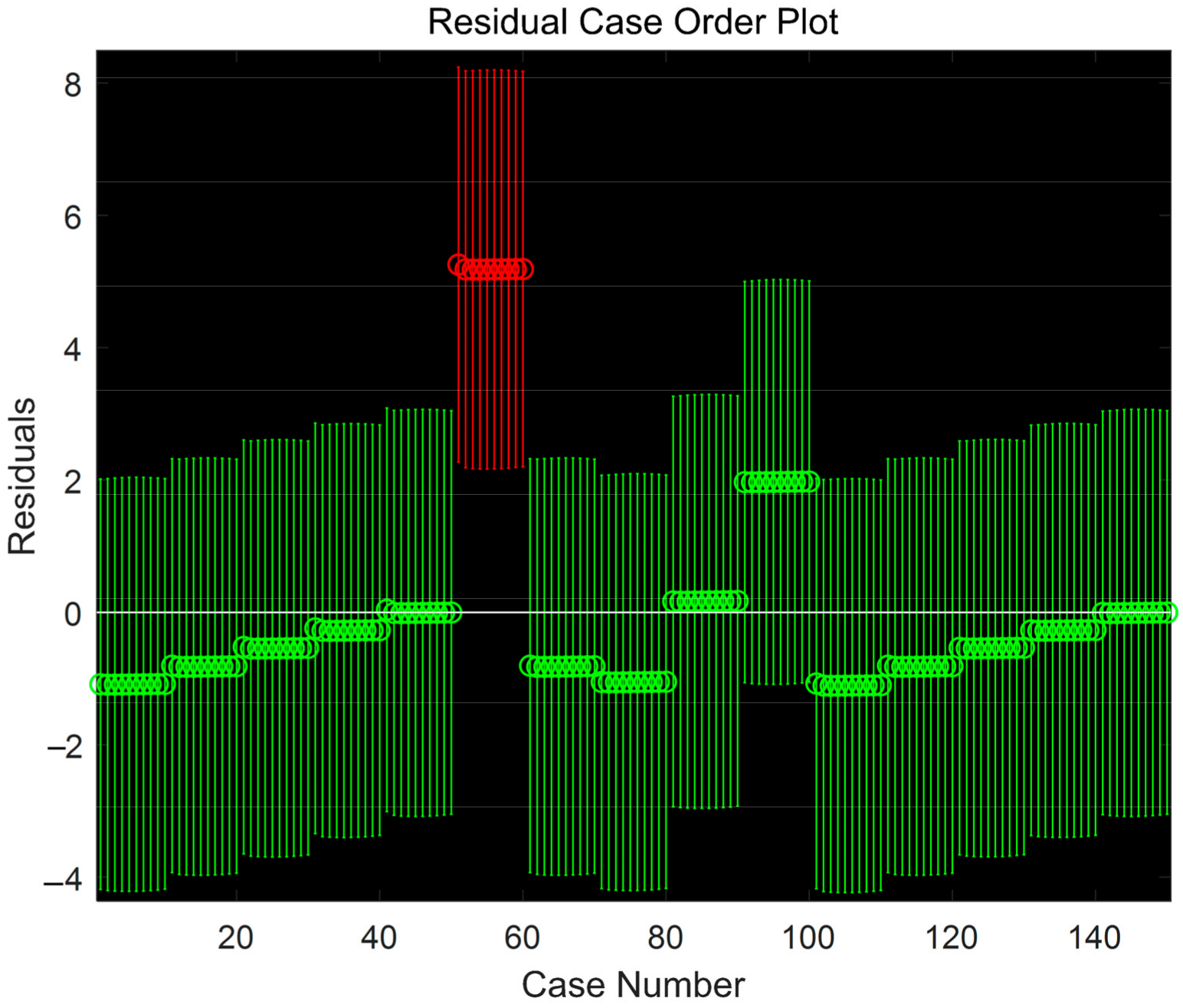
6. Prediction Models of Circuit Parameter

By analyzing the variation relationship of circuit parameters of the above electrode plate materials, we can see the complexity of circuit characteristics and relatively independent relationships between different influencing factors. When solving circuit parameter characteristics of graphene PD sensor, to further simplify circuit parameter calculations and facilitate engineering applications, this section establishes multiple linear regression models of three circuit parameters based on the least-square method.

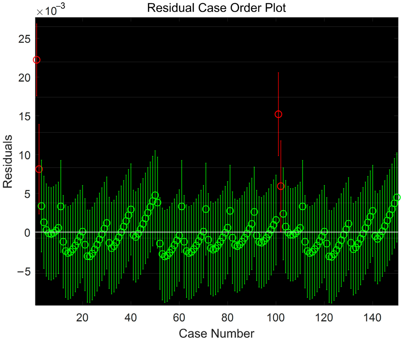
6.1. Prediction Model of Resistance

Based on the resistance characteristics, a dataset with four different influencing factors as independent variables and resistance as the dependent variable was constructed. Additionally, a scatter plot was created to view the linearity correlation between the independent variables and the predictor variables. The linearity is shown in Figure 16.
Next, the four independent variables, including width, thickness, Fermi energy level, and the number of layers, were used to establish a multiple linear regression equation with the resistance. Additionally, the regression coefficients corresponding to the four independent variables were calculated using the least-square method. The regression equation is as follows:
R w , t , E F , N = 10 5 × ( 1384.8 17.813 w 3.5347 t 353.47 E F 82.028 N )
To further validate the above regression equation, the residuals of the 150 data samples were plotted as shown in Figure 17.
Figure 17 shows that only four data points are outliers, indicating that the regression equation is valid for a good fit to the data.

6.2. Prediction Model of Inductance

Based on the inductance characteristics, a dataset with four different influencing factors as independent variables and inductance as the dependent variable was constructed. Additionally, a scatter plot was created to view the linearity correlation between the independent variables and the predictor variables. The linearity is shown in Figure 18.
Next, the four independent variables, including width, thickness, Fermi energy level, and the number of layers, were used to establish multiple linear regression equations with the inductance. Additionally, the regression coefficients corresponding to the four independent variables were calculated using the least-square method. The regression equations were obtained as follows:
L w , t , E F , N = 10 5 × ( 112 . 87 4 . 1833 w + 5 . 8543 t 42 . 905 E F + 2 . 0733 N )
To further validate the above regression equation, the residuals of the 150 data samples were plotted as shown in Figure 19.
Figure 19 shows that only 10 data points are outliers, indicating that the regression equation is valid for a good fit to the data.

6.3. Prediction Model of Capacitance

Based on the capacitance characteristics, a dataset with four different influencing factors as independent variables and capacitance as the dependent variable was constructed. Additionally, a scatter plot was created to view the linearity correlation between the independent variables and the predictor variables. The linearity is shown in Figure 20.
Next, the four independent variables, including width, thickness, Fermi energy level, and the number of layers, were used to establish multiple linear regression equations with the capacitance. Additionally, the regression coefficients corresponding to the four independent variables were calculated using the least-square method. The regression equations were obtained as follows:
C w , t , E F , N = 7 . 2635 + 0 . 41265 w 0 . 26849 t 2 . 6119 E F 1 . 3563 × 10 3 N  
To further validate the above regression equation, the residuals for the 150 data samples were plotted as shown in Figure 21.
Figure 21 shows that only 10 data points are outliers, indicating that the regression equation is valid for a good fit to the data.

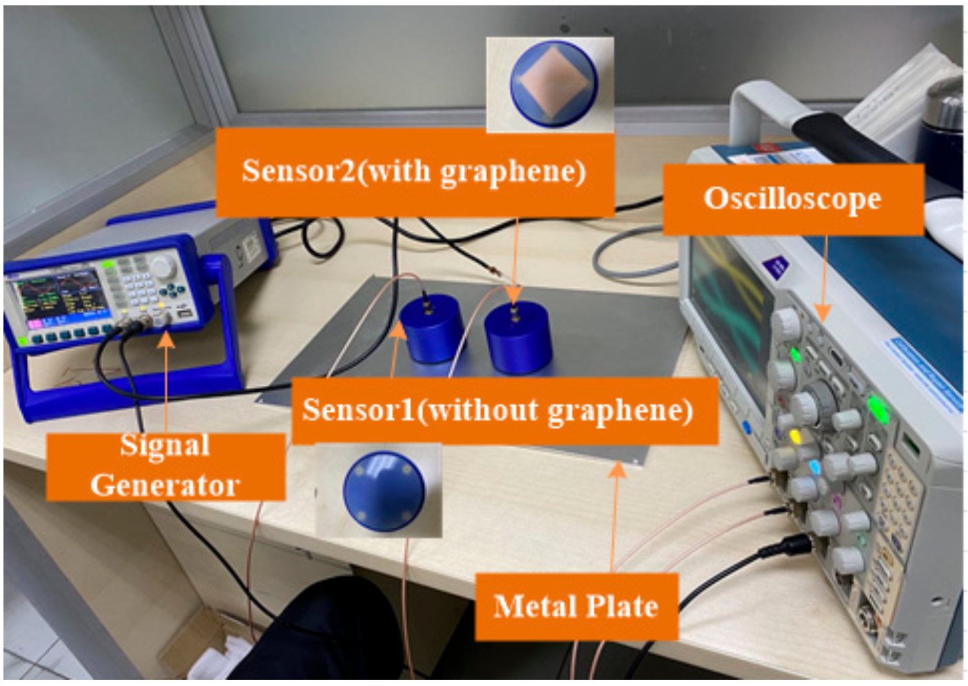
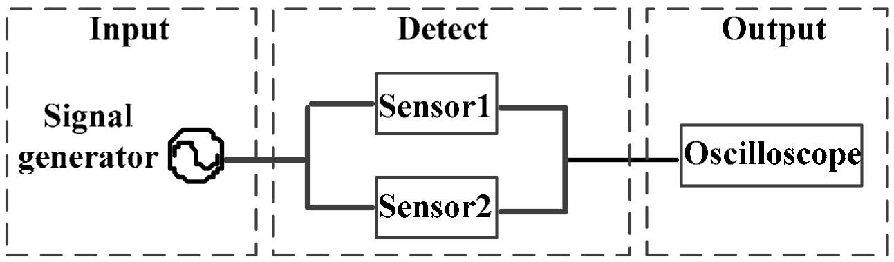
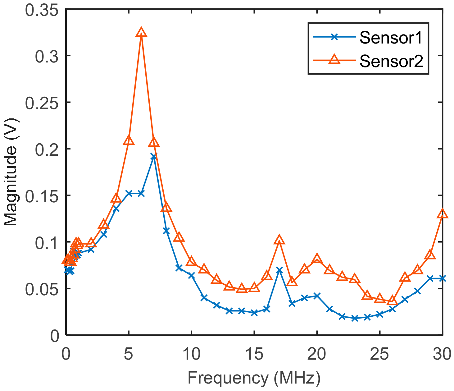
7. Simulation and Experimental Analysis

7.1. Simulation Analysis

In the simulation part, the above circuit parameter characteristics can be used to construct a drive-transfer-load circuit model. In this way, the transfer characteristics of the electrode plate can be analyzed. Figure 22 and Figure 23 are the simulation circuit models of the graphene copper-clad electrode plate and the traditional copper electrode plate, respectively.
In Figure 22 and Figure 23, Part1 is the drive section, Part2 is the transfer section, Part3 is the load section.
Based on the above circuit models, the transmission matrices of graphene copper-clad electrode plates TG and that of traditional copper electrode plates TCu can be expressed as:
T G = 1 R d 0 1 1 0 s C d 1 1 R ESC 0 1 1 s L ESC 0 1 1 0 s C ESC 1 = A G B G C G D G
T Cu = 1 R d 0 1 1 0 s C d 1 1 R C u 0 1 = A Cu B Cu C Cu D Cu
where, s = jw. Based on the relationship between output and input described by the transmission matrix, the transmission characteristic of the simulated system can be obtained as:
G s = V o V i = 1 A + s B C L
when the parameters are set as, driving resistance Rd = 50 kΩ, driving capacitance Cd = 1 aF, load capacitance CL = 1 aF, w = 20 nm, t = 20 nm, N = 1, l = 1 mm, the frequency characteristics of graphene copper-clad electrode plates with different Fermi energy levels and pure copper electrode plates can be obtained by Matlab simulation as shown in Figure 24.
Figure 24 shows that the graphene copper-clad electrode plate can improve the gain of the transmitted signal. As the Fermi energy level of graphene increases, the number of carriers involved in the transport in its conduction band increases. The transmission characteristics are better than the traditional copper plate.

7.2. Experimental Analysis

This section presents experiments to validate the results of the theoretical study and simulation. Two experimental studies are carried out. The experiment of sensor characteristics validates the frequency-domain characteristics and time-domain characteristics of the graphene PD sensor. The experiment of partial discharge detection of switchgear validates the sensing ability of the graphene PD sensor in a real partial discharge situation.

7.2.1. Experiment of Sensor Characteristics

In the experimental part, in order to obtain the frequency characteristics of the two sensors, a sensor testing and verification platform was built in the laboratory. This platform mainly consists of a signal generator, two sensors, a metal plate, and an oscilloscope. Two traditional TEV sensors with the same configuration are selected. In sensor1, the electrode plate is copper. In sensor2, in order to be consistent with the simulation, single-layer graphene copper-clad electrode plate has commissioned a manufacturer to process. Next, the original copper electrode plate is replaced by this electrode plate, and 1 V sine signals of different frequencies are produced through the signal generator, which is connected to a metal plate. The metal plate can be used to simulate the surface of the switchgear. Two sensors are placed on the metal plate to detect the signal generated by the generator, and the detected signals are transmitted to an oscilloscope via BNC connections. The peak-to-peak values of the detected waveforms can be recorded for analysis of the frequency characteristics.
Figure 25 shows the experimental setup of the frequency characteristics test system. Figure 26 shows the electrical diagram of the experimental setup. During this experiment, the signal generator is used to produce the frequency signal from 0 to 30 MHz. The magnitude of the detection voltage of each adjustment process is recorded and the frequency characteristic curve of the sensor is plotted, as shown in Figure 27. The x-coordinate is the frequencies of the input sine signal, and the y-axis is the amplitude of the voltage signal.
Figure 27 shows that the gain of the graphene partial discharge sensor (sensor2) is effectively improved compared with the traditional sensor, which is consistent with the simulation results.
In order to obtain the pulse signal response characteristics, the signal generator is used to produce 1 V pulse voltage, with frequency to 10 MHz, pulse signal rising edge time to 100 ns. The impulse response characteristics are plotted based on the data from the two sensor outputs.
Figure 28 shows that sensor2 (with graphene) has a higher capacity to couple signals than sensor1 (without graphene) in the time domain.

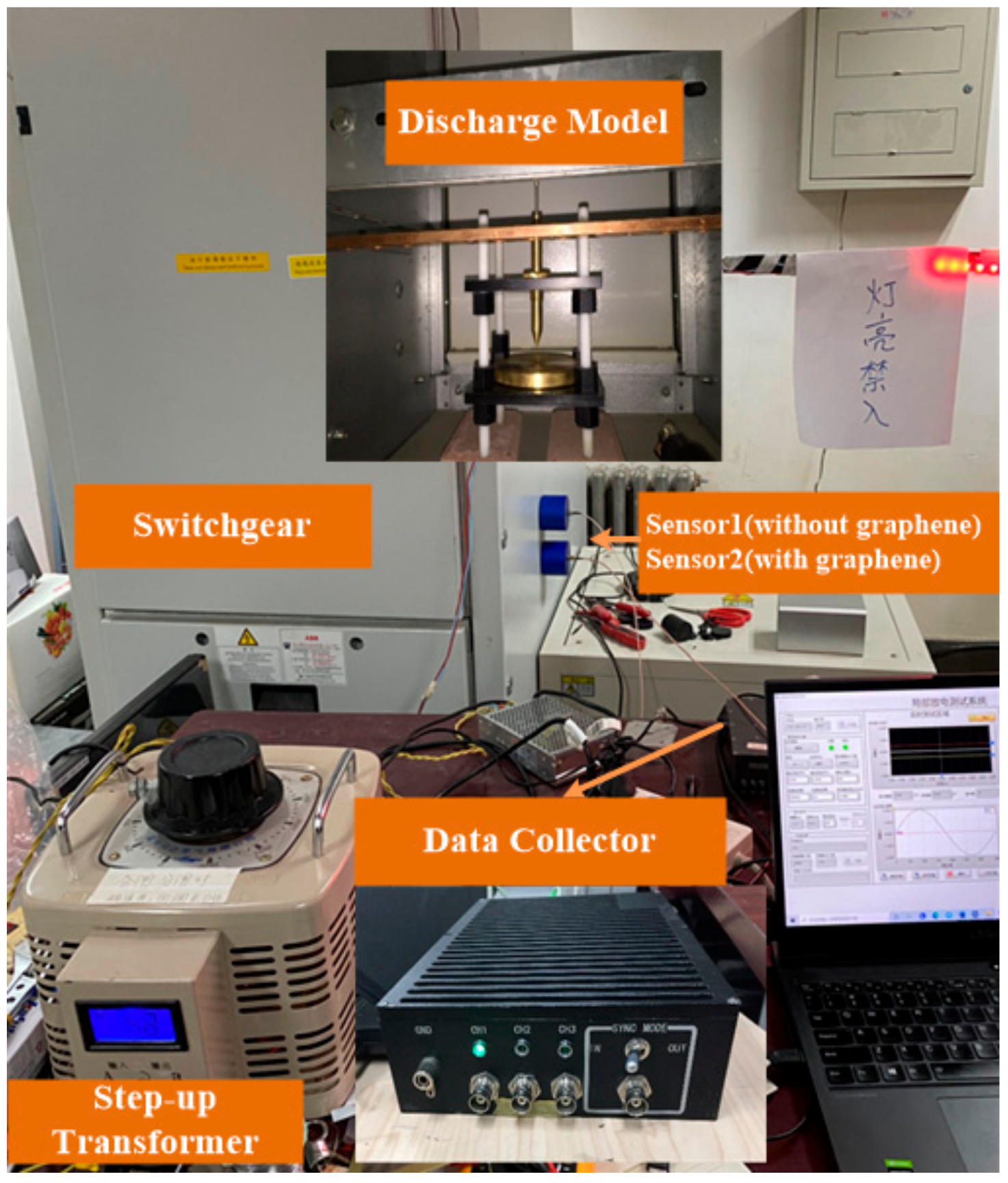
7.2.2. Experiment of Partial Discharge Detection of Switchgear

In order to further test the sensing ability of the graphene sensor on the partial discharge, the switchgear partial discharge detection system was built. The experimental detection system mainly includes an AC power supply, step-up transformer for exciting partial discharge, switchgear, discharge model, two sensors, data collector.
Figure 29 shows the experimental setup of partial discharge detection of switchgear. Figure 30 shows the electrical diagram of the experimental setup. The discharge model has been placed inside the switchgear in advance and two sensors are placed on the surface of the switchgear. Sensor1 (without graphene) is connected to the CH2 channel of the data collector and sensor2 (with graphene) is connected to the CH3 channel. When the voltage of the step-up transformer is regulated to 4.8 kV, the discharge model inside the switchgear produces partial discharge. The partial discharge signals sensed by the two sensors can be collected through the data collector.
Figure 31 shows that the gain of sensor2 (with graphene) is higher than sensor1 (without graphene) for the same single partial discharge pulse, which is consistent with the theoretical simulation results.

8. Conclusions

Aiming at the design of new graphene PD sensors, the paper proposes a method to analyze the circuit parameter characteristics of electrode plate material of graphene PD sensors. This method can lay the foundation for further analysis of the propagation characteristics and further design of graphene PD sensor material structure.
The main conclusions of this paper are obtained as:
  • Resistance gradually decreases with the increasing number of layers. The greater the width and Fermi energy level, the lower the equivalent resistance. The total thickness has less effect on the resistance;
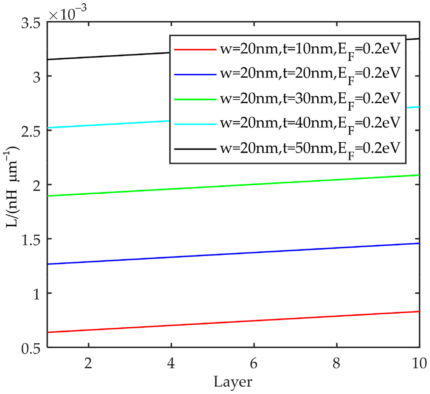
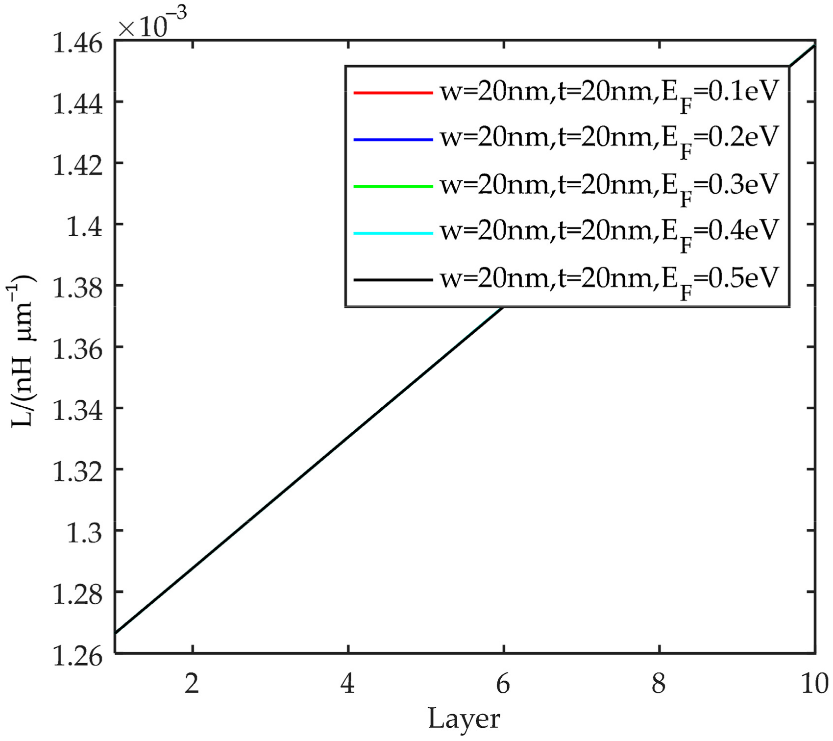
  • Inductance gradually increases with the number of layers, but the overall change is small. The greater the width, the lower the total inductance of the electrode plate, but the total thickness is the opposite. The Fermi energy level does not affect the inductance;
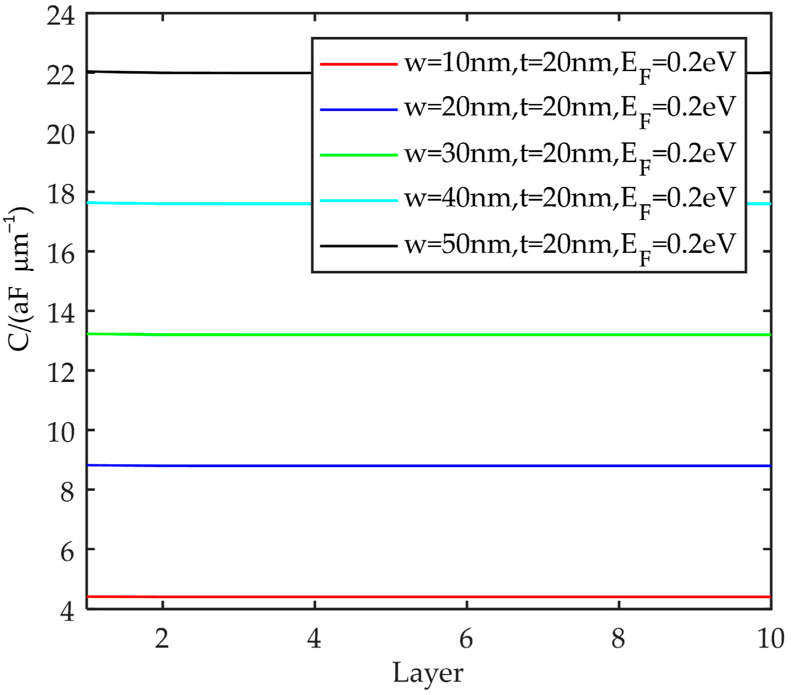
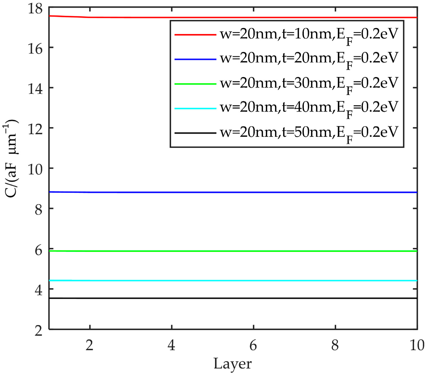
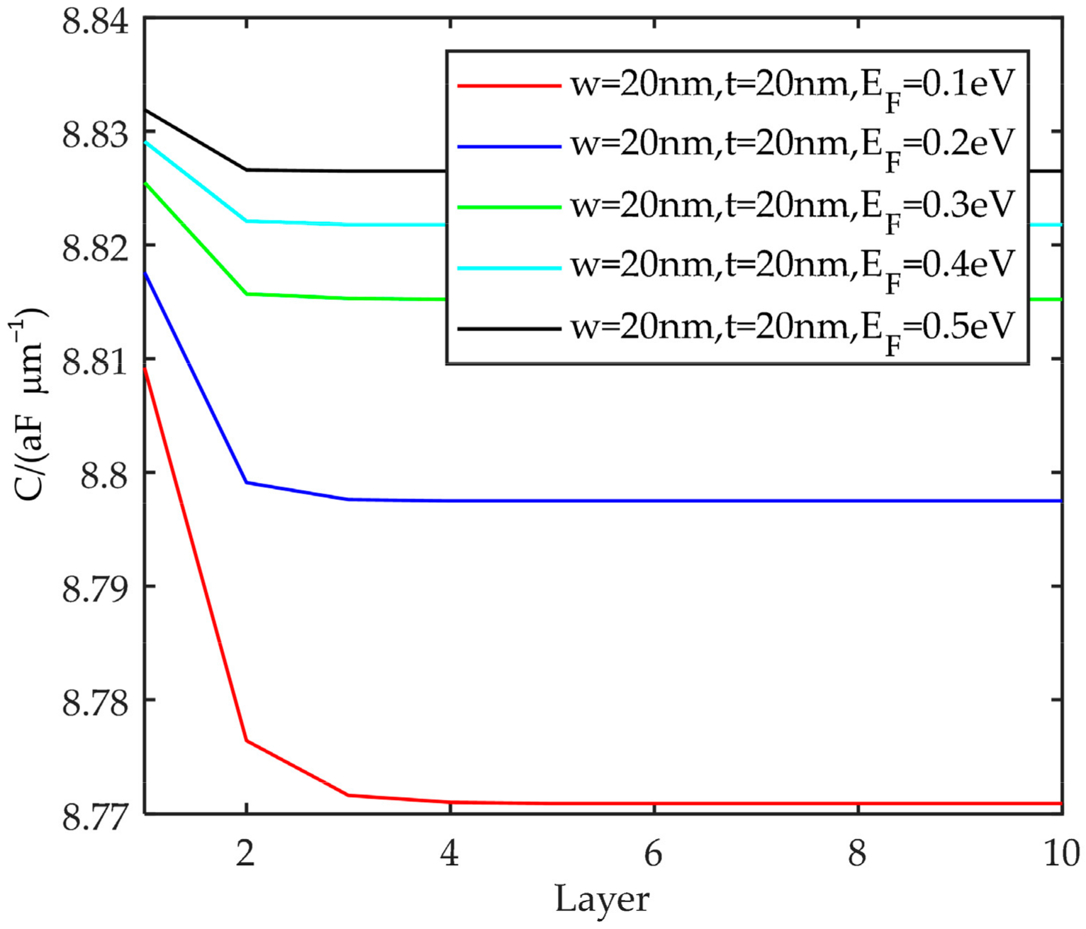
  • Capacitance gradually decreases with the increase of the number of layers, but the trend is flat. With the increase of the width, the capacitance gradually increases. The thickness has the opposite effect on the capacitance. The Fermi energy level becomes larger, and the equivalent capacitance tends to increase.
  • Multiple linear regression models based on the least-square method were established for three circuit parameters, which can further simplify the calculation of circuit parameters and provide a good fit of the data.
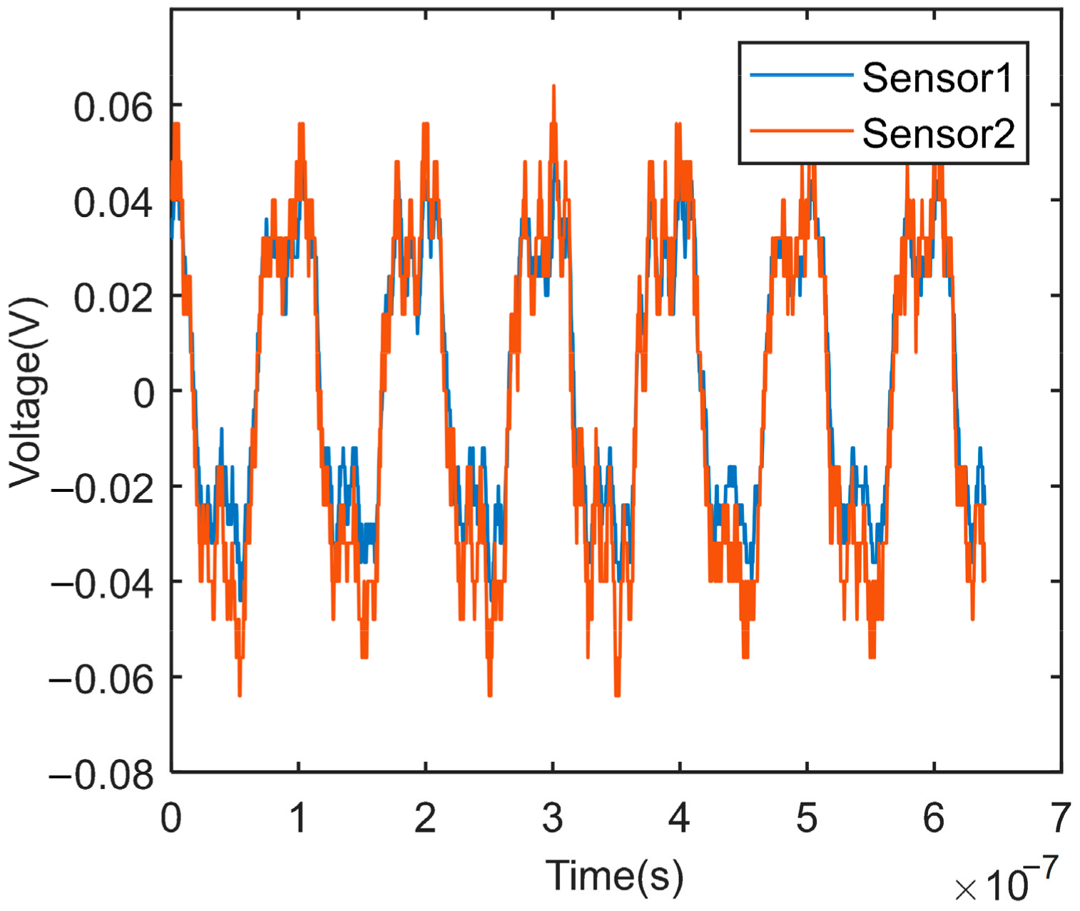
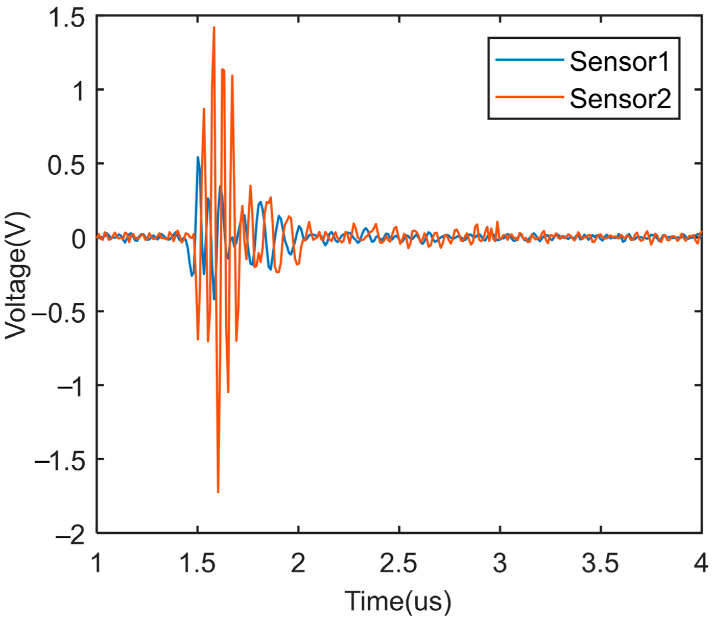
  • Simulation and experimental results verify that the graphene PD sensor exhibits high gain characteristics compared to the traditional PD sensor.

Author Contributions

Conceptualization, H.Z. and Z.W.; methodology, H.Z.; software, H.Z.; formal analysis, Z.W.; validation, H.Z. and Z.W.; writing—original draft preparation, H.Z.; writing—review and editing, H.Z.; supervision, Z.W. All authors have read and agreed to the published version of the manuscript.

Funding

This research was funded by the National Key Research and Development Program of China under Grant 2018YFB2100104.

Institutional Review Board Statement

Not applicable.

Informed Consent Statement

Not applicable.

Data Availability Statement

Not applicable.

Conflicts of Interest

The authors declare no conflict of interest.

References

  1. Zhang, S.Y.; Mei, J.; Zheng, J.Y.; Mei, F. Research on a Multilayer Distributed Online Monitoring System of 10 kV High Voltage Switchgear. In Proceedings of the 2013 4th International Conference on Digital Manufacturing & Automation (ICDMA), Qingdao, China, 29–30 June 2013; pp. 1025–1028. [Google Scholar]
  2. Knezev, M.; Djekic, Z.; Kezunovic, M. Automated Circuit Breaker Monitoring. In Proceedings of the 2007 IEEE Power Engineering Society General Meeting (PES), Tampa, FL, USA, 24–28 June 2007; pp. 1–6. [Google Scholar]
  3. Ruan, W.-C.; Yao, Y.; Ouyang, X.-D.; Zeng, G.-W.; Su, C.; Xia, Z.-Q. Study on the reliability of 10kV uninterrupted maintenance outgoing switchgear under the condition of main device switching to the back-up device. In Proceedings of the 2020 IEEE International Conference on High Voltage Engineering and Application (ICHVE), Beijing, China, 6–10 September 2020; pp. 1–4. [Google Scholar]
  4. Qian, Y.; Huang, W.; Li, D.; Zhang, H.; Liu, P.; Peng, Z. Optimization design of bushing of distribution switchgear equipment. In Proceedings of the 2016 IEEE International Conference on High Voltage Engineering and Application (ICHVE), Chengdu, China, 19–22 September 2016; pp. 1–4. [Google Scholar]
  5. Yao, Y. Study on Design of Main Busbar System of Large-current High-voltage Switchgear. In Proceedings of the 2020 Asia Energy and Electrical Engineering Symposium (AEEES), Chengdu, China, 29–31 May 2020; pp. 12–15. [Google Scholar]
  6. Ji, Y.; Nie, Y.; Lin, X.; Qiu, H.; Wang, X.; Pan, J. Research on 3D Electric Field Distribution of 12 kV Switchgear Based on ANSYS. In Proceedings of the 2020 8th International Conference on Power Electronics Systems and Applications (PESA), Hong Kong, China, 7–10 December 2020; pp. 1–6. [Google Scholar]
  7. Zeng, X.; Li, H.; Lu, Y.; Chen, Y. Online monitoring of partial discharge in high voltage switchgear using a differential electric field sensor. In Proceedings of the 2017 IEEE Conference on Electrical Insulation and Dielectric Phenomenon (CEIDP), Fort Worth, TX, USA, 22–25 October 2017; pp. 385–388. [Google Scholar]
  8. Li, J.; Zhang, X.; Han, X.; Yao, X. A Partial Discharge Detection Method for SF6 Insulated Inverted Current Transformers Adopting Inner Shield Case as UHF Sensor. IEEE Trans. Power Deliv. 2018, 33, 3237–3239. [Google Scholar] [CrossRef]
  9. Li, Y.; Lu, F.; Xie, H.; Wang, Y. Study on ultrasonic generation mechanism of partial discharge. In Proceedings of the 2005 International Symposium on Electrical Insulating Materials (ISEIM), Kitakyushu, Japan, 5–9 June 2005; pp. 467–471. [Google Scholar]
  10. Rencheng, Z.; Li, X.; Liu, E.; Yang, J. Arithmetic and experiment research on ultrasonic detection of partial discharge for switchboard. In Proceedings of the 2011 IEEE International Conference on Computer Science and Automation Engineering (CSAE), Shanghai, China, 10–12 June 2011; pp. 330–334. [Google Scholar]
  11. Cullen, G.; Stewart, B.G.; Hepburn, D.M. Application of a radio frequency antenna technique for monitoring the speed, torque and internal fault conditions of A.C. and D.C. electric motors. In Proceedings of the 2004 IEEE Sensors for Industry Conference (ISA), New Orleans, LA, USA, 27–29 January 2004; pp. 50–54. [Google Scholar]
  12. Birlasekaran, S.; Leong, W.H. Comparison of Known PD Signals with the Developed and Commercial HFCT Sensors. IEEE Trans. Power Deliv. 2007, 22, 1581–1590. [Google Scholar] [CrossRef] [Green Version]
  13. Zhu, L.; Hou, F.; Ji, S.; Rehman, H.; Wu, X. Primary Differential Pulse Method for Partial-Discharge Detection of Oil-Immersed Inverted Current Transformers. IEEE Trans. Power Deliv. 2018, 33, 1492–1494. [Google Scholar] [CrossRef]
  14. Zhang, C.; Dong, M.; Ren, M.; Wang, L.; Zhou, J. High bandwidth measurement of partial discharge current pulses based on the optimized needle-plate electrode system. In Proceedings of the 2016 International Conference on Condition Monitoring and Diagnosis (CMD), Xi’an, China, 25–28 September 2016; pp. 916–919. [Google Scholar]
  15. Davies, N.; Tian, Y.; Cheung, J.; Tang, Y.; Shiel, P. Non-intrusive partial discharge measurements of MV switchgears. In Proceedings of the 2008 International Conference on Condition Monitoring and Diagnosis, Beijing, China, 21–24 April 2008; pp. 385–388. [Google Scholar]
  16. Coenen, S.; Tenbohlen, S.; Markalous, S.M.; Strehl, T. Sensitivity of UHF PD measurements in power transformers. IEEE Trans. Dielectr. Electr. Insul. 2008, 15, 1553–1558. [Google Scholar] [CrossRef]
  17. Zheng, Q.; Ma, G.; Jiang, J.; Li, C.; Zhan, H. A comparative study on partial discharge ultrasonic detection using fiber Bragg grating sensor and piezoelectric transducer. In Proceedings of the 2015 IEEE Conference on Electrical Insulation and Dielectric Phenomena (CEIDP), Ann Arbor, MI, USA, 18–21 October 2015; pp. 282–285. [Google Scholar]
  18. Fujii, Y.; Cho, H.; Nakamura, Y. Highly sensitive partial discharge detection by TEV method under severe noise conditions. In Proceedings of the 2017 4th International Conference on Electric Power Equipment—Switching Technology (ICEPE-ST), Xi’an, China, 22–25 October 2017; pp. 783–786. [Google Scholar]
  19. Subramaniam, A.; Raman, S.J.; Panda, S.K. Comparison of Partial Discharge signal in a Three phase Transformer by UHF, TEV and HFCT sensors. In Proceedings of the 2021 1st International Conference on Power Electronics and Energy (ICPEE), Bhubaneswar, India, 2–3 January 2021; pp. 1–4. [Google Scholar]
  20. Wang, Z.; Shaygan, M.; Otto, M.; Schall, D.; Neumaier, D. Flexible Hall sensors based on graphene. Nanoscale 2016, 8, 7683–7687. [Google Scholar] [CrossRef] [PubMed] [Green Version]
  21. Friedman, A.L.; Robinson, J.T.; Perkins, F.K.; Campbell, P.M. Extraordinary magnetoresistance in shunted chemical vapor deposition grown graphene devices. Appl. Phys. Lett. 2011, 99, 022108. [Google Scholar] [CrossRef]
  22. Tamagnone, M.; Gómez-Díaz, J.S.; Mosig, J.R.; Perruisseau-Carrier, J. Reconfigurable terahertz plasmonic antenna concept using a graphene stack. Appl. Phys. Lett. 2012, 101, 214102. [Google Scholar] [CrossRef] [Green Version]
  23. Wang, J.; Lu, W.B.; Liu, Z.G.; Zhang, A.Q. Graphene-Based Microwave Antennas with Reconfigurable Pattern. IEEE Trans. Antennas Propag. 2020, 68, 2504–2510. [Google Scholar] [CrossRef]
  24. Wang, X.C.; Zhao, W.S.; Hu, J.; Yin, W.Y. Reconfigurable terahertz leaky-wave antenna using graphene-based high-impedance surface. IEEE Trans. Nanotechnol. 2015, 14, 62–69. [Google Scholar] [CrossRef]
  25. Zhang, R.; Zhao, W.S.; Hu, J.; Yin, W.Y. Electrothermal Characterization of Multilevel Cu-Graphene Heterogeneous Interconnects in the Presence of an Electrostatic Discharge (ESD). IEEE Trans. Nanotechnol. 2015, 14, 205–209. [Google Scholar] [CrossRef]
  26. Koziel, S.; Leifsson, L.; Couckuyt, I.; Dhaene, T. Fourth order hybrid implicit and explicit FDTD method. Int. J. Numer. Model 2013, 26, 493–505. [Google Scholar] [CrossRef]
  27. Kumar, V.; Rakheja, S.; Naeemi, A. Modeling and optimization for multi-layer graphene nanoribbon conductors. In Proceedings of the 2011 IEEE International Interconnect Technology Conference (IITC), Dresden, Germany, 8–12 May 2011; pp. 1–3. [Google Scholar]
  28. Rostaminia, R.; Saniei, M.; Vakilian, M. Effects of transformer core modeling on Partial Discharge current pulses simulation accuracy. In Proceedings of the 2015 IEEE 11th International Conference on the Properties and Applications of Dielectric Materials (ICPADM), Sydney, Australia, 19–22 July 2015; pp. 664–667. [Google Scholar]
  29. Amin, E.M.; Karmakar, N.C. A Passive RF Sensor for Detecting Simultaneous Partial Discharge Signals Using Time-Frequency Analysis. IEEE Sens. J. 2016, 16, 2339–2348. [Google Scholar] [CrossRef]
  30. Cheng, Z.H.; Zhao, W.S.; Dong, L.X.; Wang, J.; Zhao, P.; Gao, H.; Wang, G.F. Investigation of Copper-Carbon Nanotube Composites as Global VLSI Interconnects. IEEE Trans. Nanotechnol. 2017, 16, 891–900. [Google Scholar] [CrossRef]
  31. Cheng, Z.H.; Zhao, W.S.; Wang, D.W.; Wang, J.; Dong, L.X.; Wang, G.F.; Yin, W.Y. Analysis of Cu-Graphene Interconnects. IEEE Access 2018, 6, 53499–53508. [Google Scholar] [CrossRef]
  32. Zhao, W.S.; Fu, K.; Wang, D.W.; Li, M.; Wang, G.; Yin, W.Y. Mini-review: Modeling and performance analysis of nanocarbon interconnects. Appl. Sci. 2019, 9, 2174. [Google Scholar] [CrossRef] [Green Version]
  33. Hu, Q.H.; Zhao, W.S.; Fu, K.; Wang, D.W.; Wang, G. Electrical modeling of carbon nanotube-based shielded through-silicon vias for three-dimensional integrated circuits. Int. J. Numer. Model. Electron. Netw. Devices Fields 2021, 34, e2842. [Google Scholar] [CrossRef]
  34. Kondo, D.; Nakano, H.; Zhou, B.; Akiko, I.; Hayashi, K.; Takahashi, M.; Sato, S.; Yokoyama, N. Sub-10-nm-wide intercalated multi-layer graphene interconnects with low resistivity. In Proceedings of the 2014 IEEE International Interconnect Technology Conference (IITC), San Jose, CA, USA, 20–23 May 2014; pp. 189–192. [Google Scholar]
  35. Sarto, M.S.; Tamburrano, A. Comparative analysis of TL models for multilayer graphene nanoribbon and multiwall carbon nanotube interconnects. In Proceedings of the 2010 IEEE International Symposium on Electromagnetic Compatibility (ISEMC), Fort Lauderdale, FL, USA, 25–30 July 2010; pp. 212–217. [Google Scholar]
Figure 1. The detection principle of the TEV sensor.
Energies 15 02169 g001
Figure 2. Equivalent model of multilayer graphene.
Energies 15 02169 g002
Figure 3. Electrode plate model.
Energies 15 02169 g003
Figure 4. Equivalent resistance.
Energies 15 02169 g004
Figure 5. Equivalent inductance.
Energies 15 02169 g005
Figure 6. Equivalent capacitance.
Energies 15 02169 g006
Figure 7. Variation curve of resistance with the number of layers at different widths.
Energies 15 02169 g007
Figure 8. Variation curve of resistance with the number of layers at different thicknesses.
Energies 15 02169 g008
Figure 9. Variation curve of resistance with the number of layers at different Fermi energy levels.
Energies 15 02169 g009
Figure 10. Variation curve of inductance with the number of layers at different widths.
Energies 15 02169 g010
Figure 11. Variation curve of inductance with the number of layers at different thicknesses.
Energies 15 02169 g011
Figure 12. Variation of inductance with the number of layers at different Fermi energy levels.
Energies 15 02169 g012
Figure 13. Variation curve of capacitance with the number of layers at different widths.
Energies 15 02169 g013
Figure 14. Capacitance variation curve with the number of layers at different thicknesses.
Energies 15 02169 g014
Figure 15. Variation of capacitance with the number of layers at different Fermi energy levels.
Energies 15 02169 g015
Figure 16. Linearity of w, t, EF, N with resistance.
Energies 15 02169 g016
Figure 17. Residual plot of the resistance prediction model.
Energies 15 02169 g017
Figure 18. Linearity between w, t, EF, N with inductance.
Energies 15 02169 g018
Figure 19. Residual plot of the inductance prediction model.
Energies 15 02169 g019
Figure 20. Linearity between w, t, EF, N with capacitance.
Energies 15 02169 g020
Figure 21. Residual plot of the capacitance prediction model.
Energies 15 02169 g021
Figure 22. The simulation circuit of graphene copper-clad electrode plate.
Energies 15 02169 g022
Figure 23. The simulation circuit of the traditional copper electrode plate.
Energies 15 02169 g023
Figure 24. Frequency characteristics in simulation.
Energies 15 02169 g024
Figure 25. Experimental setup of sensor characteristics test system.
Energies 15 02169 g025
Figure 26. Electrical diagram of the experimental setup.
Energies 15 02169 g026
Figure 27. Frequency characteristics in experiment.
Energies 15 02169 g027
Figure 28. Impulse signal response characteristics.
Energies 15 02169 g028
Figure 29. Experimental setup of partial discharge detection of switchgear.
Energies 15 02169 g029
Figure 30. Electrical diagram of the experimental setup.
Energies 15 02169 g030
Figure 31. Single partial discharge pulse waveform.
Energies 15 02169 g031
Table 1. The properties of graphene.
MaterialResistivityCarrier MobilityElectrical
Conductivity
Thermal
Conductivity
Electron Transfer
Capability
Graphene10−6 Ω/cm200,000 cm2V−1S−1highhighgood
Table 2. Relationship between circuit parameters and four influencing factors.
Circuit ParameterswtEFN
Resistance\
Inductance+\+
Capacitance++
“+” represents proportional relation; “−” represents inversely proportional relation; “\” represents little relation.
Publisher’s Note: MDPI stays neutral with regard to jurisdictional claims in published maps and institutional affiliations.

