Article

Input Small-Signal Characteristics of Selected DC–DC Switching Converters

Faculty of Electronics and Computer Science, Koszalin University of Technology, Sniadeckich 2, 75-453 Koszalin, Poland
*
Author to whom correspondence should be addressed.
Energies 2022, 15(5), 1924; https://doi.org/10.3390/en15051924
Submission received: 4 February 2022 / Revised: 3 March 2022 / Accepted: 4 March 2022 / Published: 6 March 2022
(This article belongs to the Topic Power System Modeling and Control)

Abstract

:
The main goal of this study was to derive small-signal models of the input characteristics of buck, boost, and flyback converters working in continuous conduction mode (CCM) and discontinuous conduction mode (DCM). The models presented in the paper were derived using the separation of variables approach and included the parasitic resistances of all converter components. The paper features a discussion about the limitations of the model accuracy. The presented characteristics were obtained by calculation and verified by measurements. The input characteristics of converters are essential in the design of converters used in Power Factor Correction systems as well as in maximum power point tracking systems (MPPT).

1. Introduction

The analysis and design of switch-mode power converters are based on various forms of a converter description [1,2,3,4]. Special attention is usually paid to the design of the control sub-circuit or the algorithm for a given power stage of a converter. The convenient form of the converter description, useful in designing the control block, are large-signal or small-signal averaged models [4,5,6,7,8,9,10,11,12]. Such models describe the power stage of a converter in the low-frequency range, neglecting fast transients occurring in the course of switching. The small-signal transmittances of a power stage of a converter may be applied directly to the synthesis of transmittances of a control stage. The control-to-output transmittance of a power stage is most frequently used in such synthesis. The input-to-output transmittance (also known as audio susceptibility) and output impedance of a converter are also useful in the control circuit design.
The input characteristics of a power stage of a DC–DC converter have not been frequently analyzed, but their knowledge is necessary in the simulation of the interdependencies of real power sources and voltage converters and would be useful to design converters to be applied in power factor correction in rectifying systems or for maximum power point tracking in photovoltaic systems [13,14,15,16]. The description of the input characteristics of switching converters is presented in some papers in the context of the input filter design, where the small-signal impedance of the converter is analyzed. The typical object of such description is a converter with a closed control loop that assures the constant output voltage and, as a consequence, the constant output power. For the lossless power stage, the input power is also constant; therefore, the input current is inversely proportional to the input voltage, so the differential input resistance is negative. The input filter design in such a situation has been considered in various studies [17,18,19,20,21,22,23].
The small-signal input characteristics of three basic DC-DC converters, i.e., buck, boost, and flyback, are discussed in this paper. The input characteristics of converters are essential in the design of converters used in Power Factor Correction systems as well as in maximum power point tracking systems (MPPT). In particular, the Γ quantity is needed for designing the control blocks of these converters. The characteristics were obtained by measurements and by calculations based on averaged, small-signal transmittances in the analytical form. Two operation modes were considered: continuous conduction mode (CCM) and discontinuous conduction mode (DCM). The power stage diagrams of the converters shown in Figure 1 were used to derive the averaged models and, in particular, the analytical description of the small-signal transmittances. In the description of currents, voltages, and some other quantities, small letters with capital subscripts (e.g., vG) denote the instantaneous values, capital letters with capital subscripts (e.g., VG) denote DC terms, and capital letters with small subscripts (e.g., Vg) denote s-domain representations of the small-signal terms of given quantities.
The instantaneous value of the input voltage is denoted by vG, and the load conductance by G. In some equations in the following text, the load resistance R = 1/G is used for convenience. The transistors and diodes are represented in Figure 1 as switches with series parasitic resistances RT and RD, respectively. The transformer in the flyback converter is represented by the pair of controlled sources and a magnetizing inductance L (the same symbol as that for the inductance of the coil in buck and boost converters). The parasitic resistances of inductors, capacitors, and transformer are RL, RC, RL1, and RL2.
The starting point for finding the analytical formulas for input transmittances of converters are the small-signal averaged models of their power stages in the form of proper equivalent circuits. The averaged models of switch-mode DC–DC converters may be obtained in several ways, as has been well described in the literature. The traditional methods presented among the others in textbooks (for example [1,2]) and papers (for example [4,5,6,7,8]) are based on the so-called state-space averaging [5,6] or switch averaging approach [7,8]. Another approach to average model creation is based on the separation of variables [24,25]. The averaged models of ideal simple converters working in continuous conduction mode (CCM), obtained by the three mentioned methods, are identical. Models for DCM obtained by the switch averaging approach differ from models obtained by the two other methods. The models of simple converters like buck, boost, and buck–boost, obtained by the switch averaging method are of the second order (two poles in the small-signal transmittance) [8,26,27], whereas the models obtained by state-space averaging or separation of variables are of the first order (single-pole transmittances) [5,6,24,25]. The analytical description of the input transmittances of non-ideal converters in the present paper is based on the averaged models derived by the separation of variables approach. Such large-signal and small-signal models for buck and boost converters have been presented in previous works [24,25], and their small-signal versions are shown in Section 2. The small-signal input transmittances of ideal buck and boost converters were presented [28] with very limited experimental verification. The influence of the parasitic resistances of a converter’s components on its characteristics is indisputable for converters working in CCM [29], but may be probably neglected in DCM because the operation in DCM corresponds to lower values of the load current and other currents in the power stage; therefore, the voltage drops due to parasitic resistances are small in DCM. Neglection of the parasitic resistances in the average description of converters in DCM is considered in this study and will be verified by measurements.
The small-signal models of a flyback converter have not been so far derived with the separation of variables approach. The averaged description of a flyback converter, convenient for finding the small-signal input characteristics, is derived in Section 3 from the known, large-signal averaged model [30,31]. The small-signal input characteristics derived from the models are discussed in Section 4 and Section 5. Examples of the measurements and numerical calculations are shown in Section 6 and Appendix A. Concluding remarks are presented in Section 7.

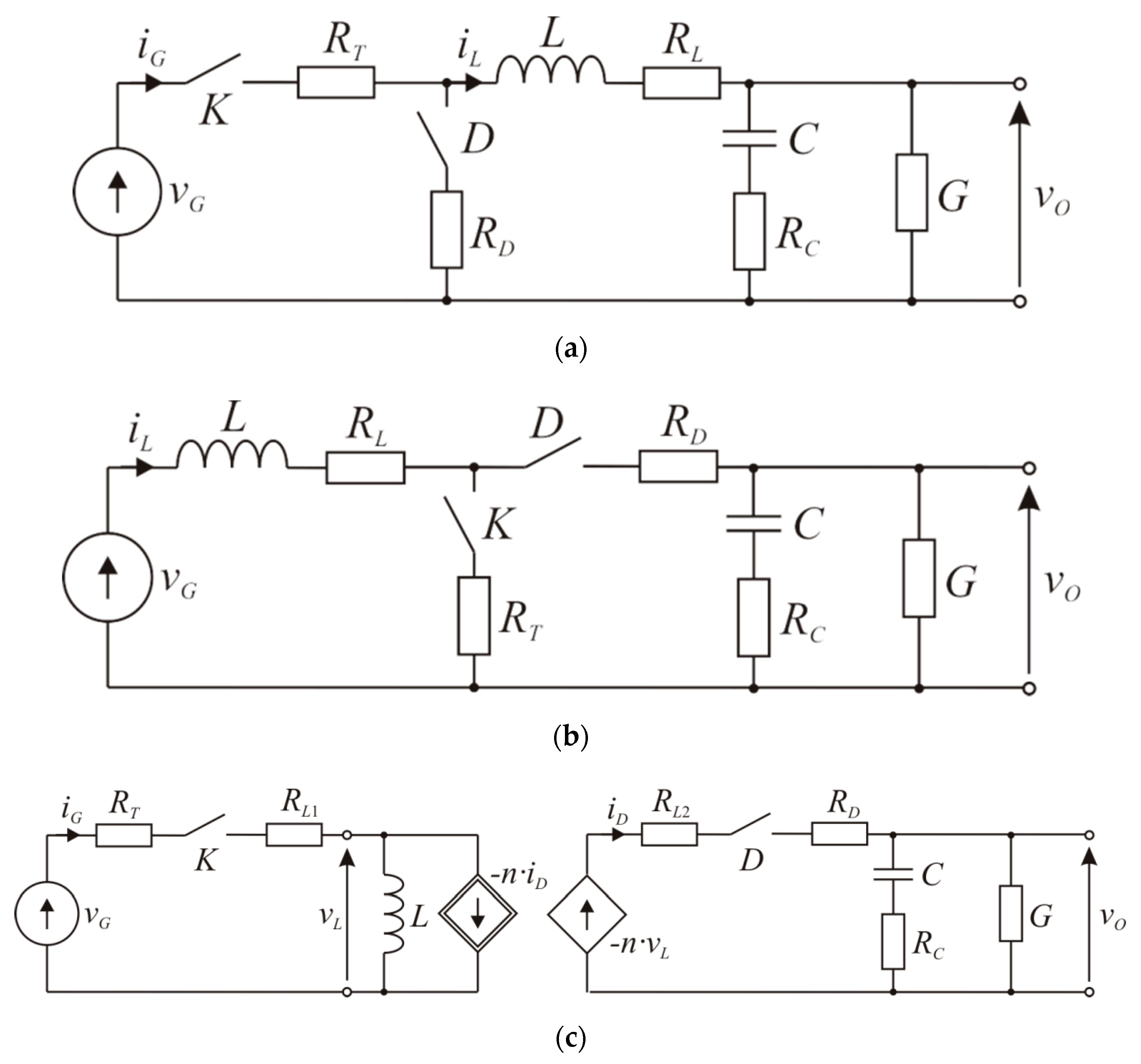
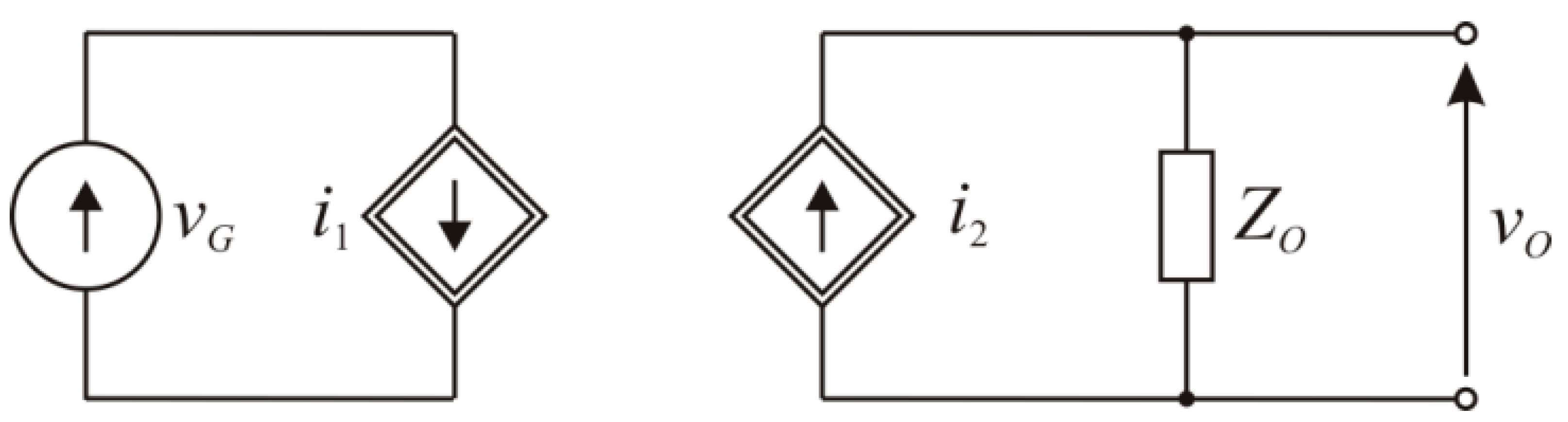
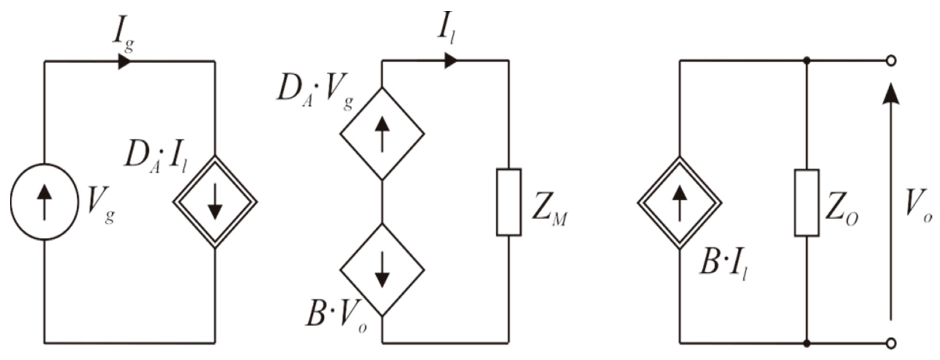
2. Small-Signal Averaged Models of Buck and Boost Converters

Large-signal and small-signal averaged models of non-ideal buck and boost converters for CCM and DCM operation mode, derived by the separation of variables, have been presented in the form of equivalent circuits [25] and may be utilized here. The small-signal models shown in Figure 2, Figure 3, Figure 4 and Figure 5 were obtained by a simple modification of the models previously described [25].
In Figure 2 and Figure 3:
Z O = s · C · R C + 1 s · C Z + G
C Z = C · ( 1 + R C · G )
Z L = s · L + R Z = s · L + R L + D A · R T + ( 1 D A ) · R D
V Z = V G + ( R D R T ) · I L
V X = V O + ( R D R T ) · I L
The symbols IL and VO denote DC terms of inductor current and output voltage in both converters.
The small-signal models of buck and boost converters working in DCM can be presented in a unified form as in Figure 4 [25]. The same scheme can be applied to a flyback converter in DCM.
The equations describing the parameters of the above models for non-ideal buck and boost converters have been reported [25]. According to the assumption in Section 1, the parasitic resistances of converters are neglected for DCM, and the resulting formulas for input transmittances of buck and boost are consistent with those previously reported [26].

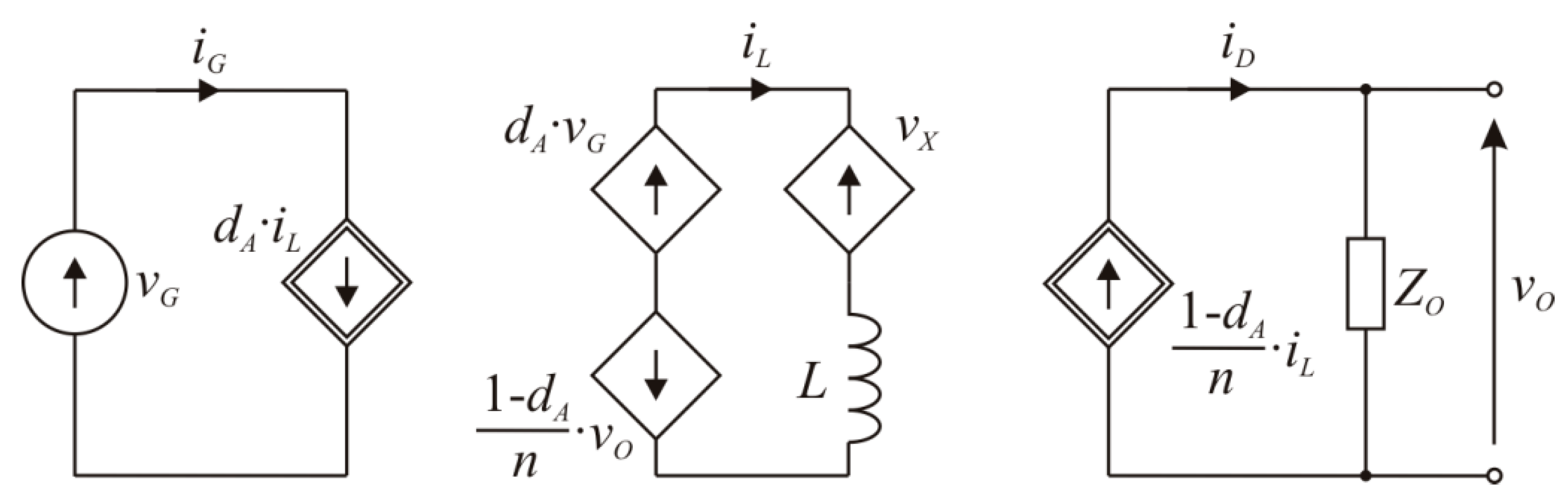
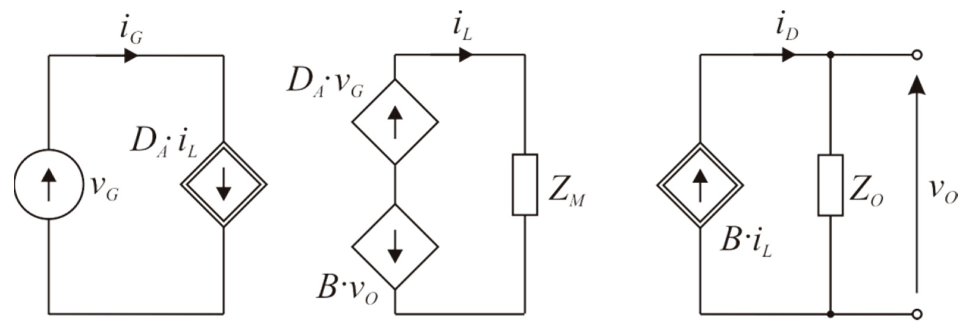
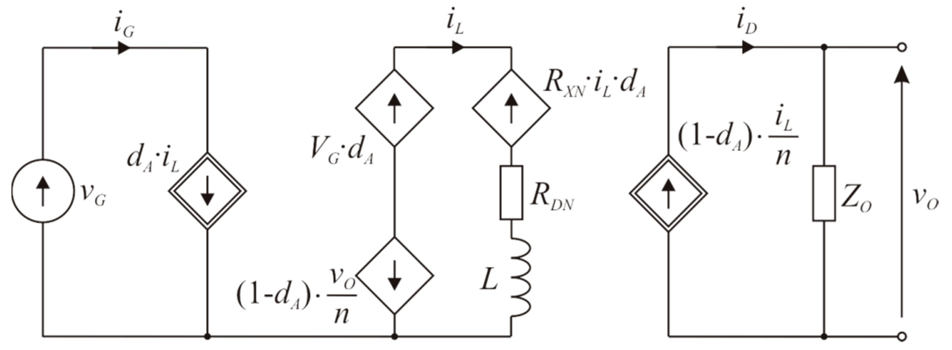
3. Averaged Models of Flyback Converter

The starting point for establishing small-signal averaged models of flyback converters is represented by the large-signal models described in [30] and shown in Figure 5 and Figure 6 for CCM and DCM, respectively.
The quantity vX in Figure 5 is [31]:
v X = i L · [ d A · R T L + ( 1 d A ) · R D L n 2 ]
and
R T L = R T + R L 1
R D L = R D + R L 2
A more detailed description of the controlled current sources presented in Figure 6 is given below [30,31,32]:
i 1 = v G 2 · L · d A 2 · T S
and
i 2 d A 2 · T S · v G 2 2 · L · v O · ( 1 v G · R D L · d A · T S v O · n · L )
The small-signal models for flyback converters in CCM and DCM may be obtained from the above, large-signal models but in the case of CCM, the derivation of full small-signal models seems not to be necessary because the input quantities defined in the next section are obtained for specific conditions—for constant duty ratio dA or constant input voltage vG. Therefore, the simplified versions of large-signal models of flyback converters in CCM, corresponding to the above conditions, were determined first and used for obtaining the simplified, specific forms of small-signal models.
The general, large-signal averaged model of a flyback converter in CCM, shown in Figure 5, includes five nonlinear sources, controlled by products of signal quantities—for example dA·iL. The structure of the large-signal model of a flyback converter in CCM for dA = const = DA, shown in Figure 7, is similar to that in Figure 5, but all controlled sources in the simplified model are linear. The large-signal model of a flyback converter in CCM for constant input voltage is shown in Figure 8.
In Figure 7 and Figure 8:
B = 1 D A n
R M = D A · R T L + ( 1 D A ) · R D L n 2
Z M = R M + s · L
R X N = R T L R D L n 2
R D N = R D L n 2
ZM and RM are defined by (12) and (13), similarly as ZL and RZ for buck and boost converters (see Equation (3)), but the quantities RTL and RDL, defined by Equations (7) and (8), were used instead of RT and RD.
The small-signal models of flyback converters in CCM, corresponding to the models from Figure 7 and Figure 8, are shown in Figure 9 and Figure 10, respectively. Note that the conditions dA = const or vG = const in large-signal models are equivalent to the conditions θ = 0 or Vg = 0 in small-signal models.
In Figure 10:
V W = V G + V O n R X N · I L
The considerations of the large-signal models of a flyback converter in DCM for two special cases, i.e., dA = const or vG = const, were unnecessary because the current i1 in Equation (9) is independent of the output voltage vO, and the resulting model was simpler than that for CCM.

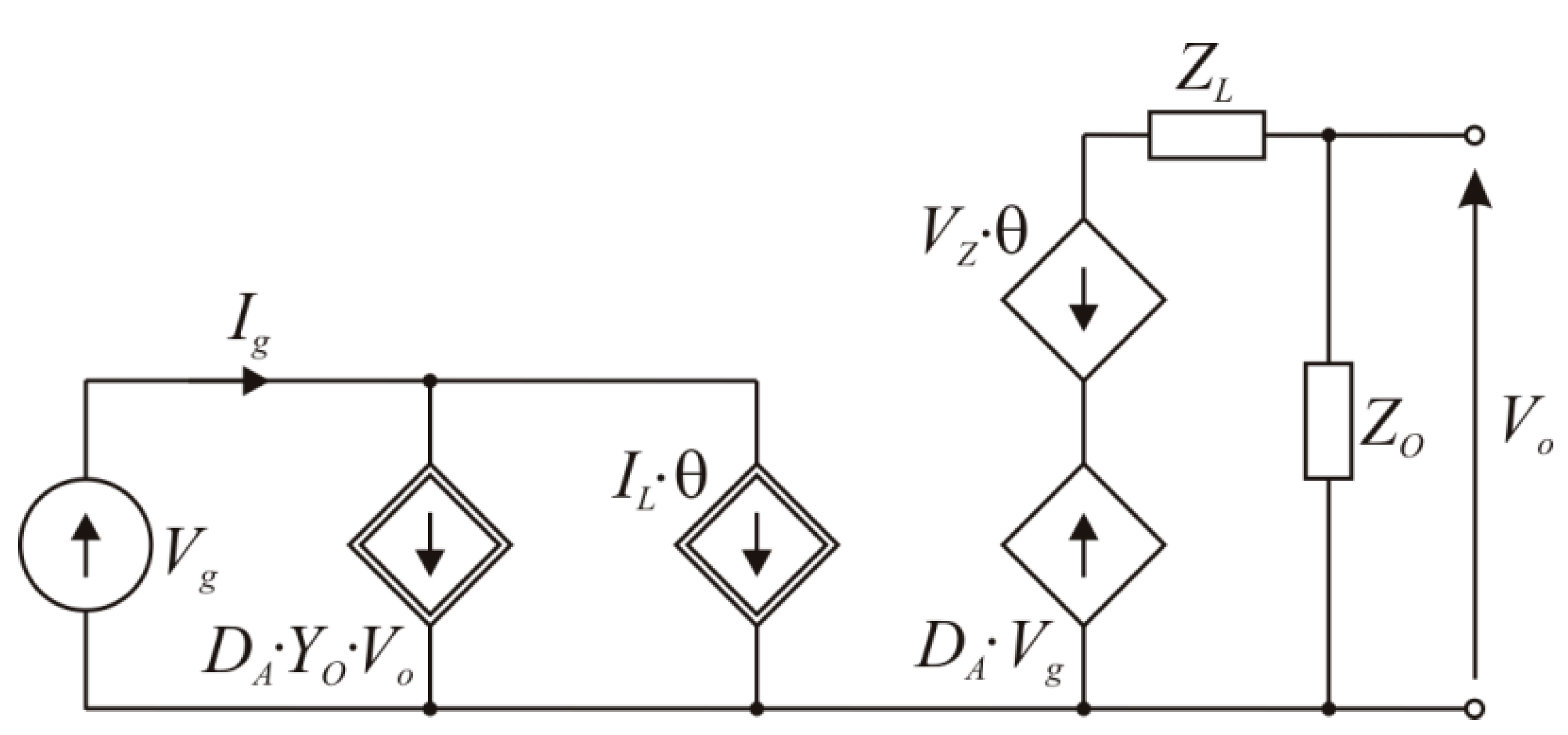
4. Small-Signal Input Characteristics for CCM

In the next step, the small-signal input characteristics in the frequency domain were calculated from the small-signal models. The general form of the input characteristics is:
I g = Y · V g + Γ · θ
where Y is the input admittance:
Y = I g V g | θ = 0
and Γ is a coefficient representing the influence of the control signal on the input current:
Γ = I g θ | V g = 0
Buck
From Equations (18) and (19) and the equivalent circuit in Figure 2, we obtain:
Y ( b u c k , C C M ) = D A 2 · ( s · C Z + G ) s 2 · L · C Z + s · ( L · G + R Z · C Z + R C · C ) + G · R Z + 1
Γ ( b u c k , C C M ) = D A · V Z · ( s · C Z + G ) s 2 · L · C Z + s · ( L · G + R Z · C Z + R C · C ) + G · R Z + 1 + I L
Low-frequency values of Y and Γ are:
Y o ( b u c k , C C M ) = D A 2 R + R Z
Γ o ( b u c k , C C M ) = D A · V Z · G G · R Z + 1 + I L
Boost
From Equations (18) and (19) and the equivalent circuit in Figure 3 we obtain:
Y ( b o o s t , C C M ) = s · C Z + G s 2 · L · C Z + s · [ G · L + R Z · C Z + ( 1 D A ) 2 · C · R C ] + ( 1 D A ) 2 + G · R Z
Γ ( b o o s t , C C M ) = s · [ I G · ( 1 D A ) · C · R C + V X · C Z ] + I G · ( 1 D A ) + V X · G s 2 · L · C Z + s · [ G · L + R Z · C Z + ( 1 D A ) 2 · C · R C ] + ( 1 D A ) 2 + G · R Z
Low-frequency values of Y and Γ are:
Y o ( b o o s t , C C M ) = G ( 1 D A ) 2 + G · R Z
Γ o ( b o o s t , C C M ) = I G · ( 1 D A ) + V X · G G · R Z + ( 1 D A ) 2
Flyback
From Equation (18) and the equivalent circuit in Figure 9 we obtain:
Y ( f l y b a c k , C C M ) = D A 2 Z M + B 2 · Z O
From Equation (19) and the equivalent circuit in Figure 10 we obtain:
Γ ( f l y b a c k , C C M ) = D A · V W + I L · ( Z M + Z O · B n ) Z M + B 2 · Z O
After introducing expressions for ZO and ZM, one obtains:
Y ( f l y b a c k , C C M ) = D A 2 · ( s · C Z + G ) s 2 · L · C Z + s · ( G · L + B 2 · C · R C + C Z · R M ) + G · R M + B 2
Γ ( f l y b a c k , C C M ) = s 2 · n · I L · L · C Z + s · ( I L · B · C · R C + n · I L · L · G + n · D A · V W · C Z + n · I L · R M · C Z ) + n · G · ( I L · R M + D A · V W ) + I L · B s 2 · n · L · C Z + s · n · ( G · L + B 2 · C · R C + C Z · R M ) + n · ( G · R M + B 2 )
Low-frequency values of Y and Γ are:
Y o ( f l y b a c k , C C M ) = D A 2 · G G · R M + B 2
Γ o ( f l y b a c k , C C M ) = D A · V W · G + I L · ( G · R M + B n ) G · R M + B 2

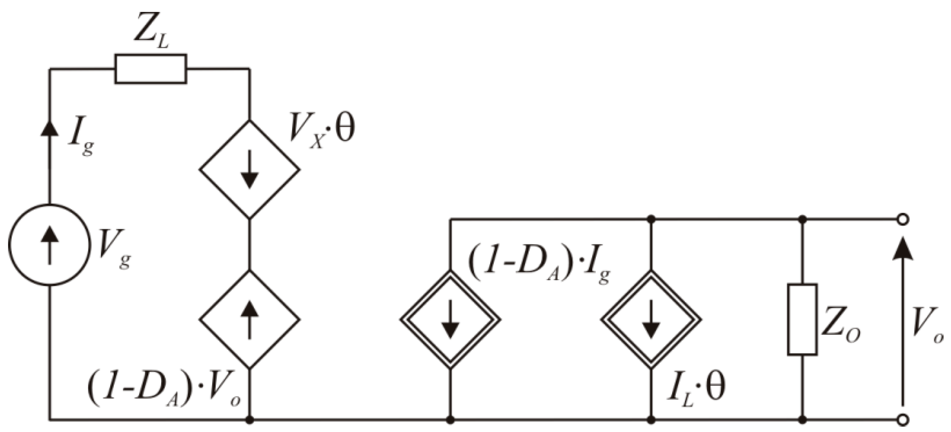
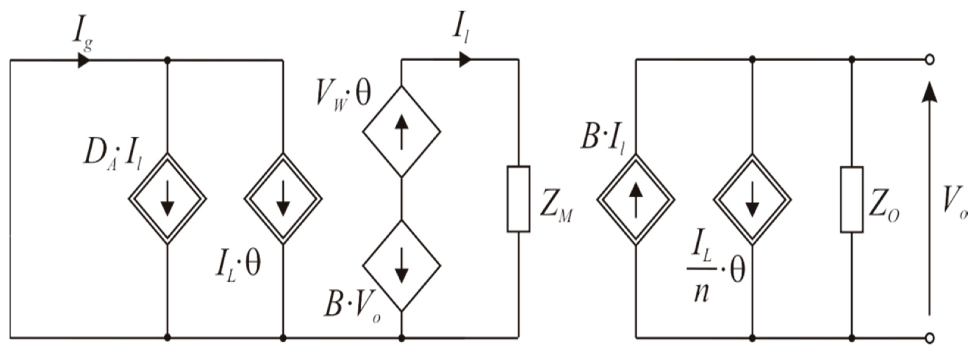
5. Small-Signal Input Characteristics for DCM

The characteristics Yin and Γ defined by Equations (18) and (19) may be found for DCM from the equivalent circuits presented in Section 2 and Section 3. For ideal buck and boost converters, these transmittances were presented in [26] and have the following general form:
Y ( D C M ) = Y o · s / ω z 1 + 1 s / ω p + 1
Γ ( D C M ) = Γ o · s / ω z 2 + 1 s / ω p + 1
where:
Y o ( b u c k , D C M ) = G A · G A · ( M I 1 ) 2 + G G A · M I 2 + G
ω Z 1 ( b u c k ) = 1 C · [ G A · ( M I 1 ) 2 + G ]
ω P ( b u c k ) = 1 C · ( G A · M I 2 + G )
Γ o ( b u c k , D C M ) = 2 · D A · G Z · ( V G V O ) · G A · ( M I 1 ) · M I + G G A · M I 2 + G
ω Z 2 ( b u c k ) = 1 C · [ G A · M I · ( M I 1 ) + G ]
Y o ( b o o s t , D C M ) = G A · G A + G · M V 2 G A + G · ( M V 1 ) 2
ω Z 1 ( b o o s t ) = G A + G · M V 2 C · M V 2
ω P ( b o o s t ) = G A + G · ( M V 1 ) 2 C · ( M V 1 ) 2
Γ o ( b o o s t , D C M ) = 2 · D A · G Z · V G · G · M V · ( M V 1 ) + G A G · ( M V 1 ) 2 + G A
ω Z 2 ( b o o s t ) = G · ( M V 1 ) · M V + G A C · ( M V 1 ) · M V
G A = D A 2 · G Z = D A 2 · T S 2 · L
The symbol MI denotes the DC current transmittance of a buck converter, and MV—DC the voltage transmittance of a boost converter.
The small-signal averaged model for a flyback converter working in DCM has the same general structure as that shown in Figure 4, but the parameter g12 is zero because the current i1 is independent of the output voltage. Only rg and β1 are necessary for finding Y and Γ, and the result is:
Y ( f l y b a c k , D C M ) = 1 / r g = D A 2 · G Z
Γ ( f l y b a c k , D C M ) = β 1 = 2 · D A · G Z · V G

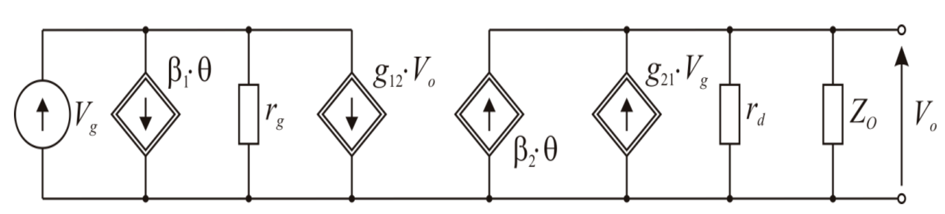
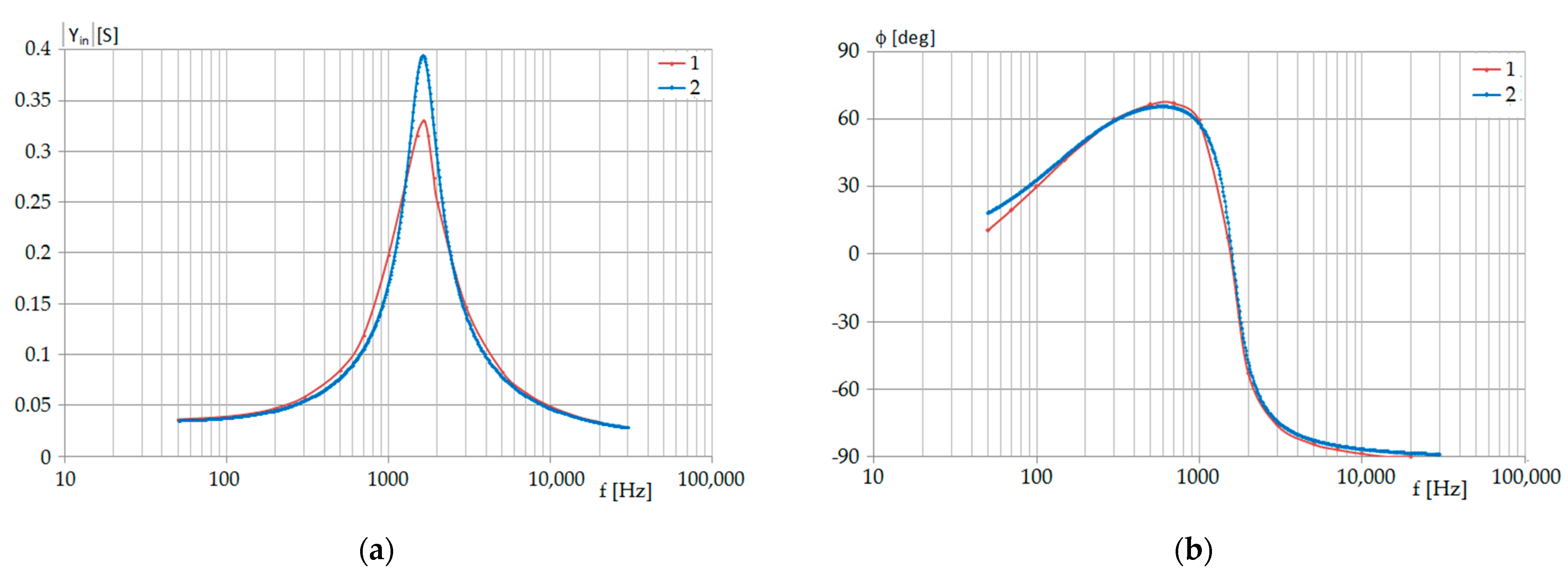
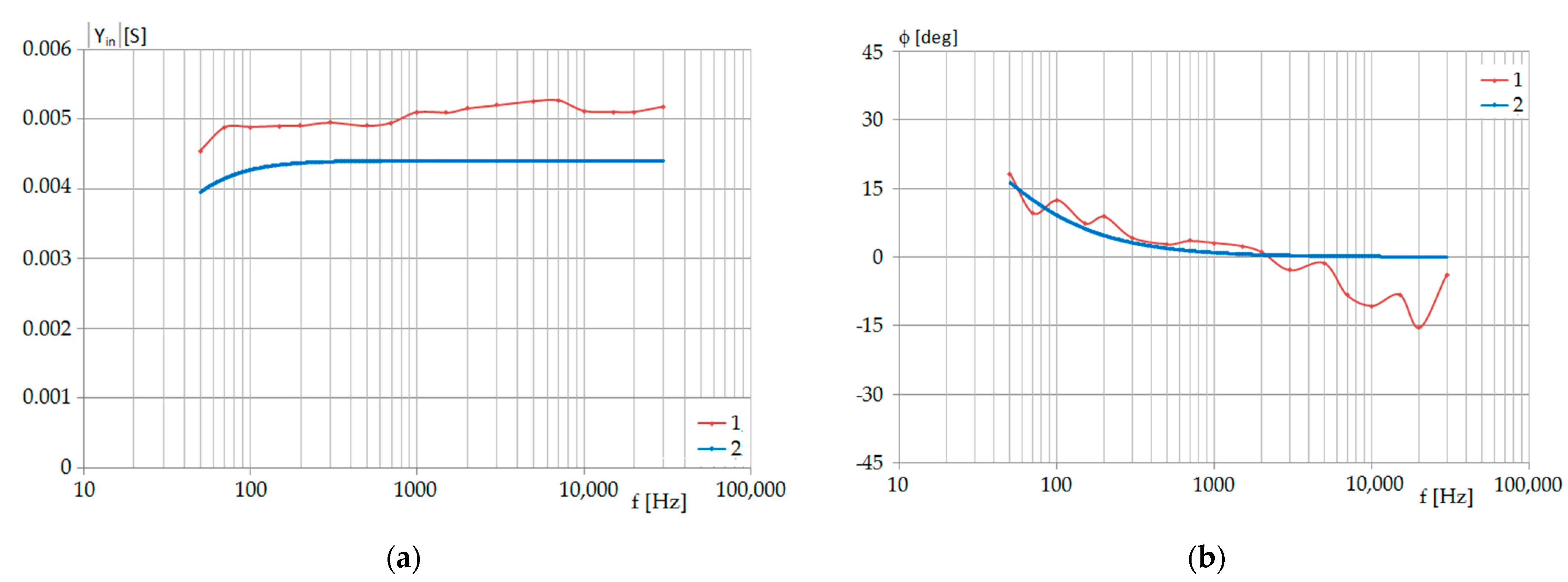
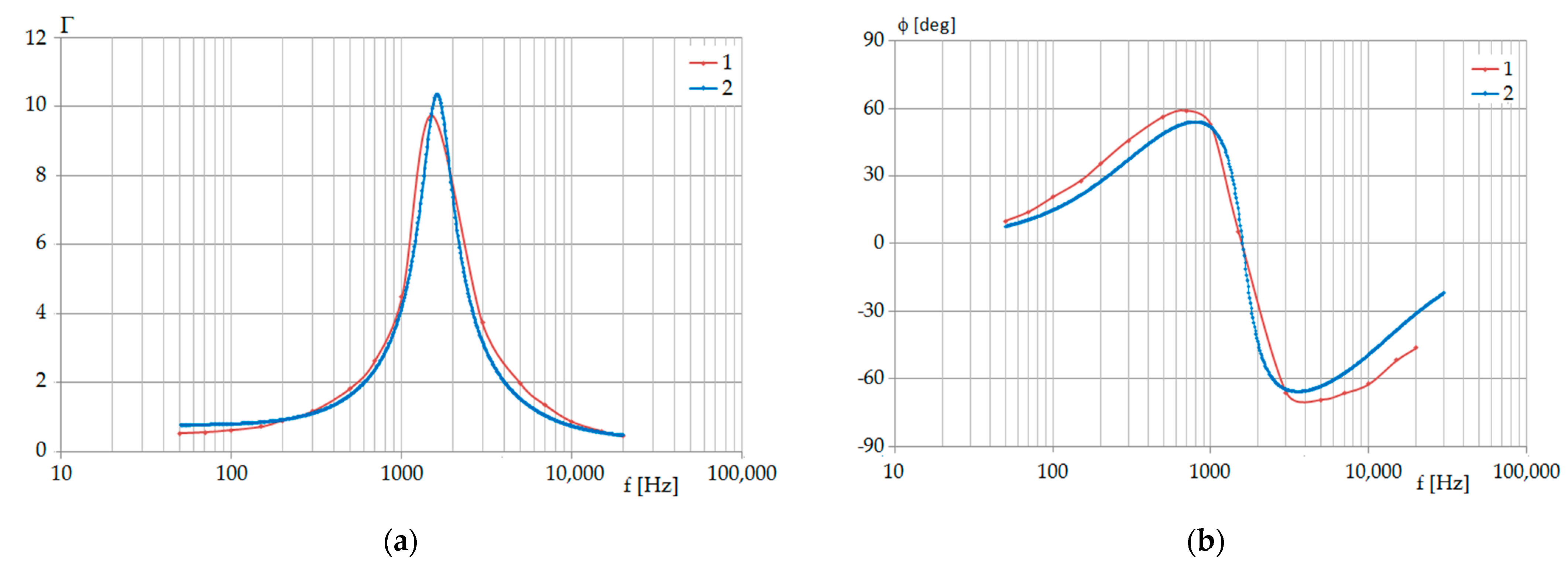
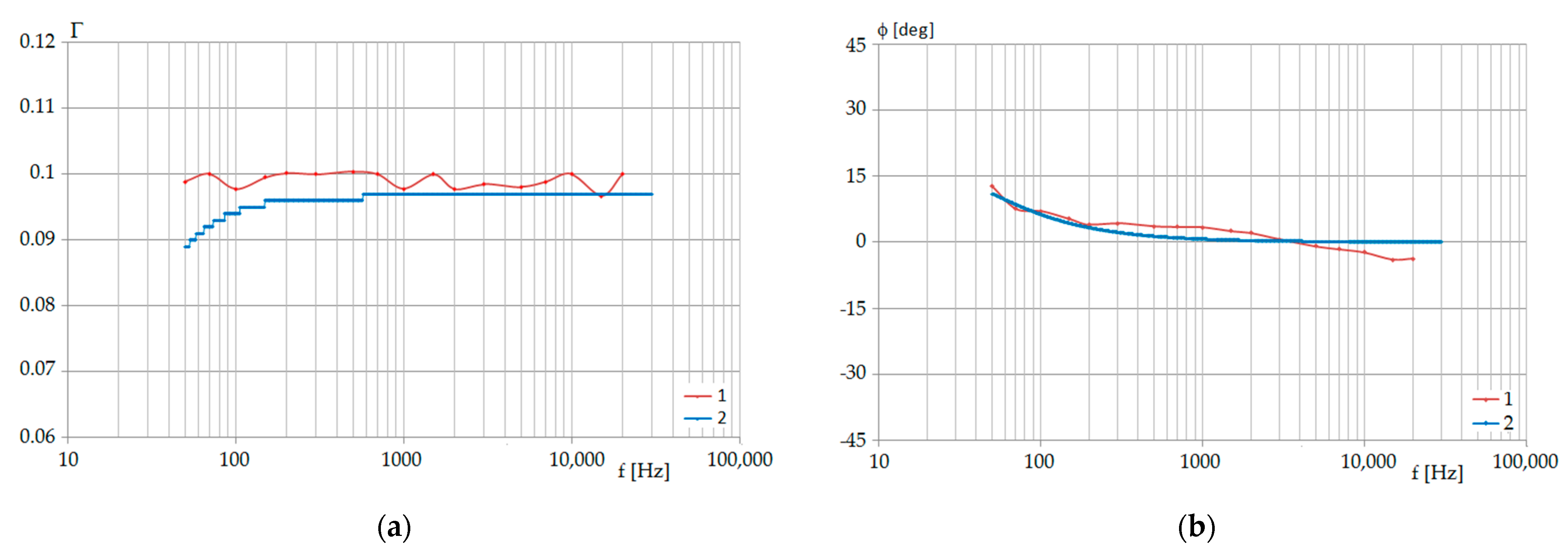
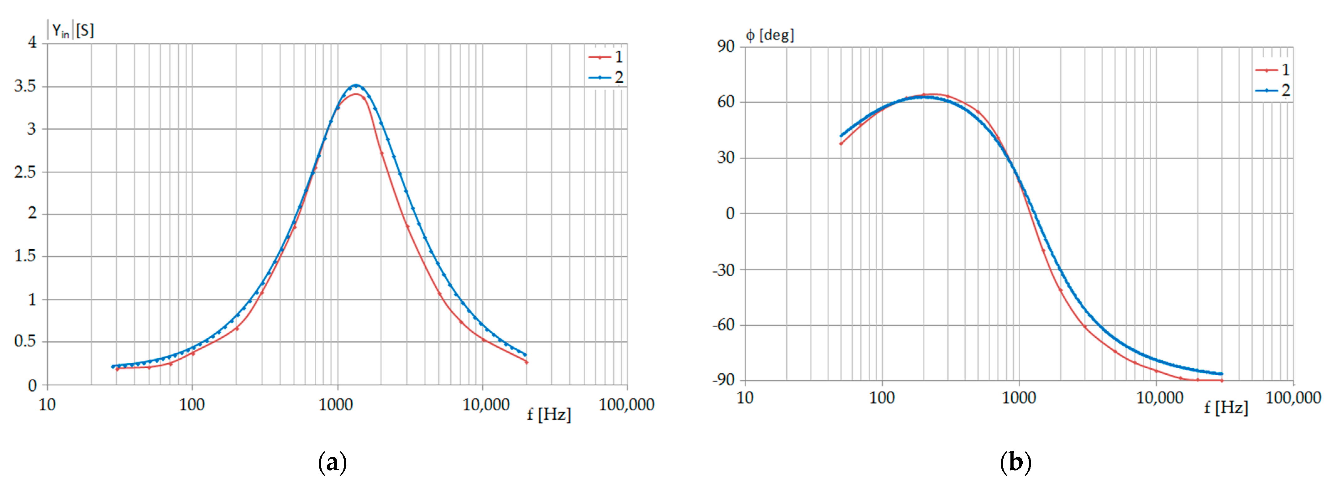
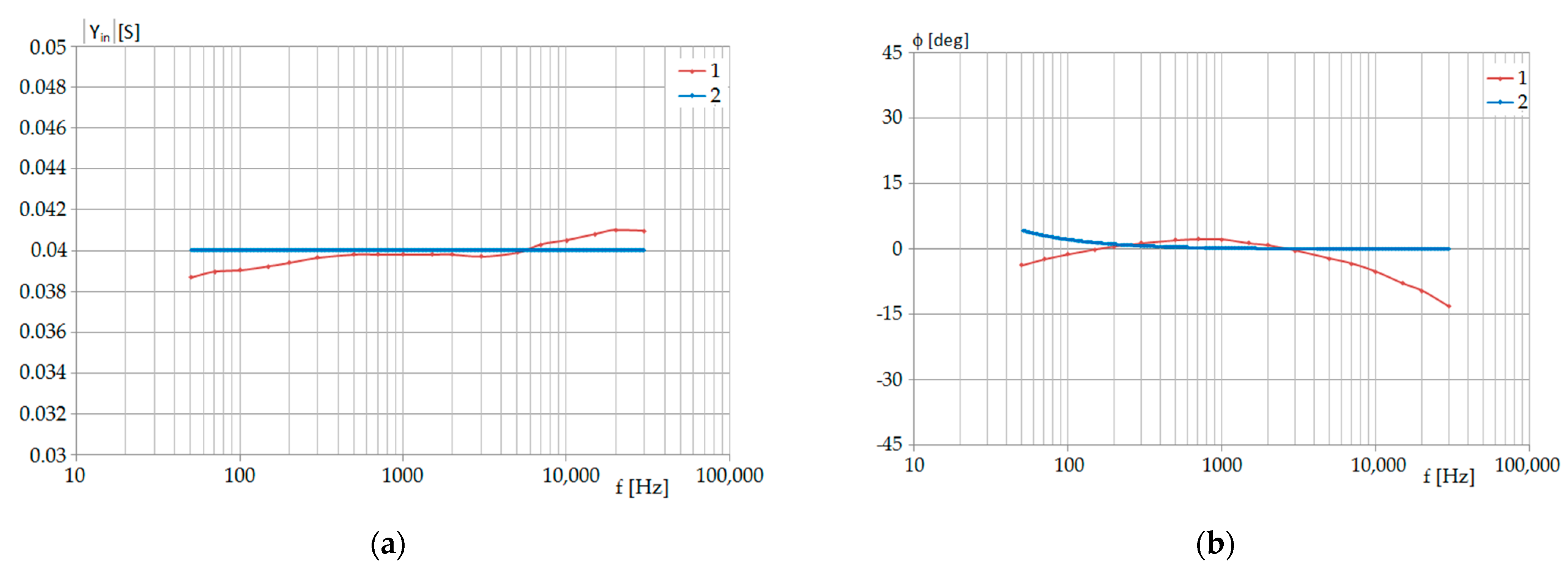
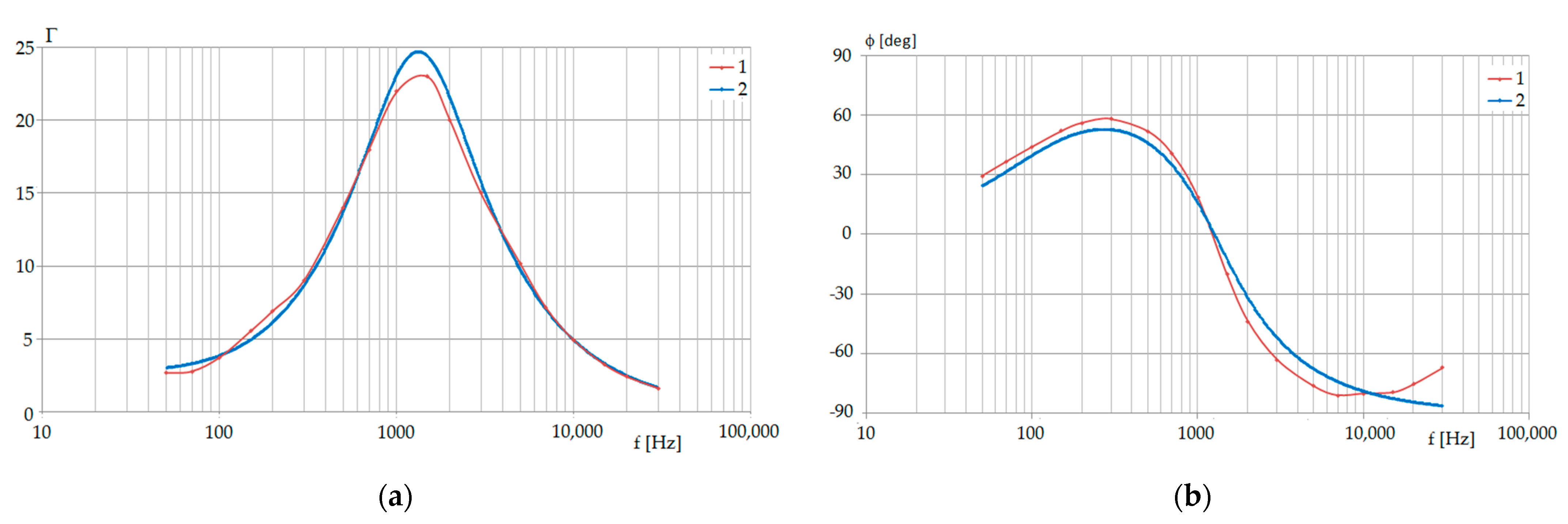
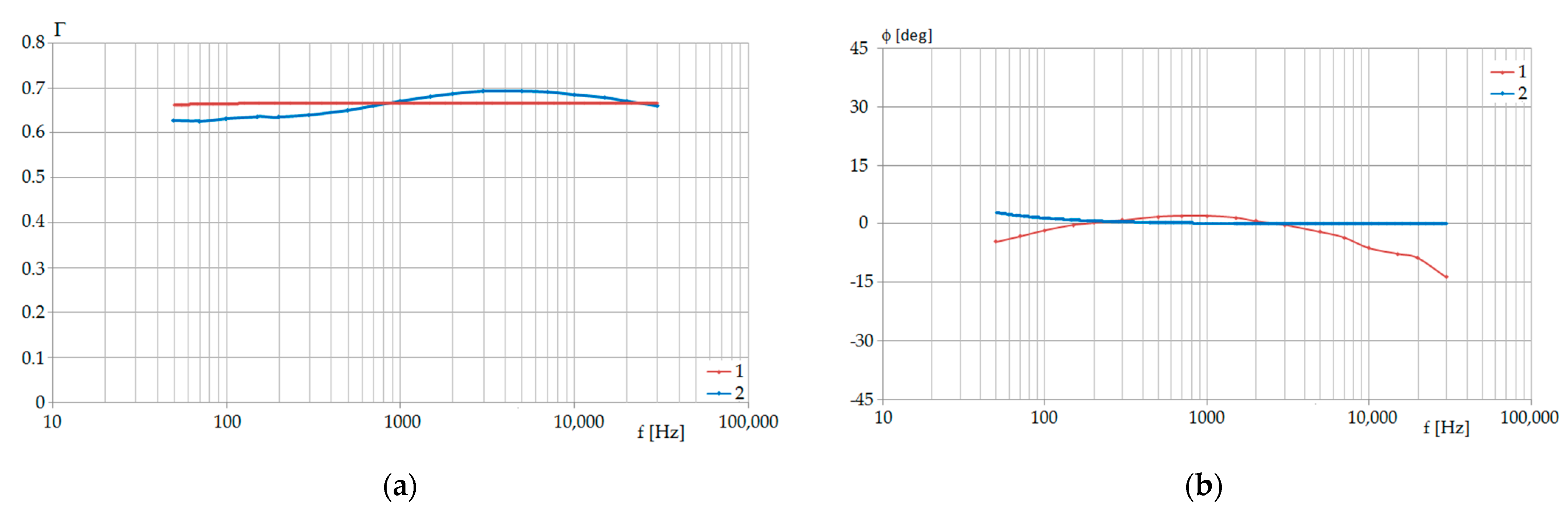
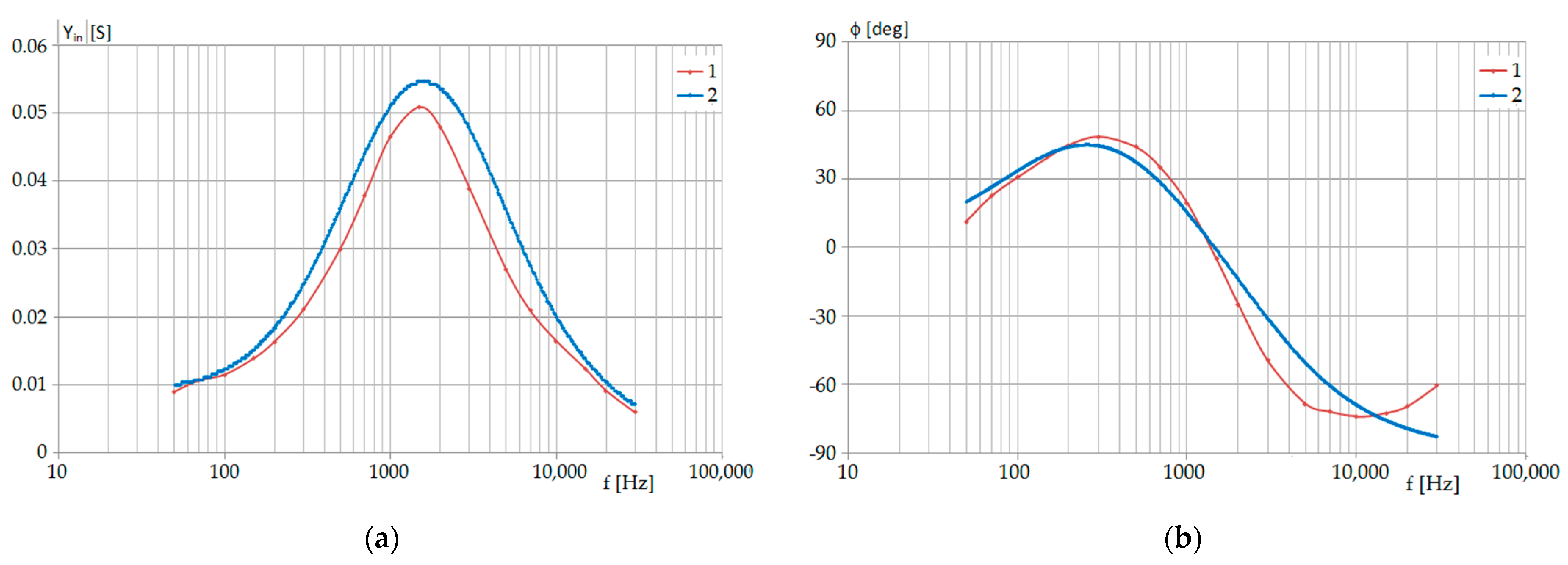
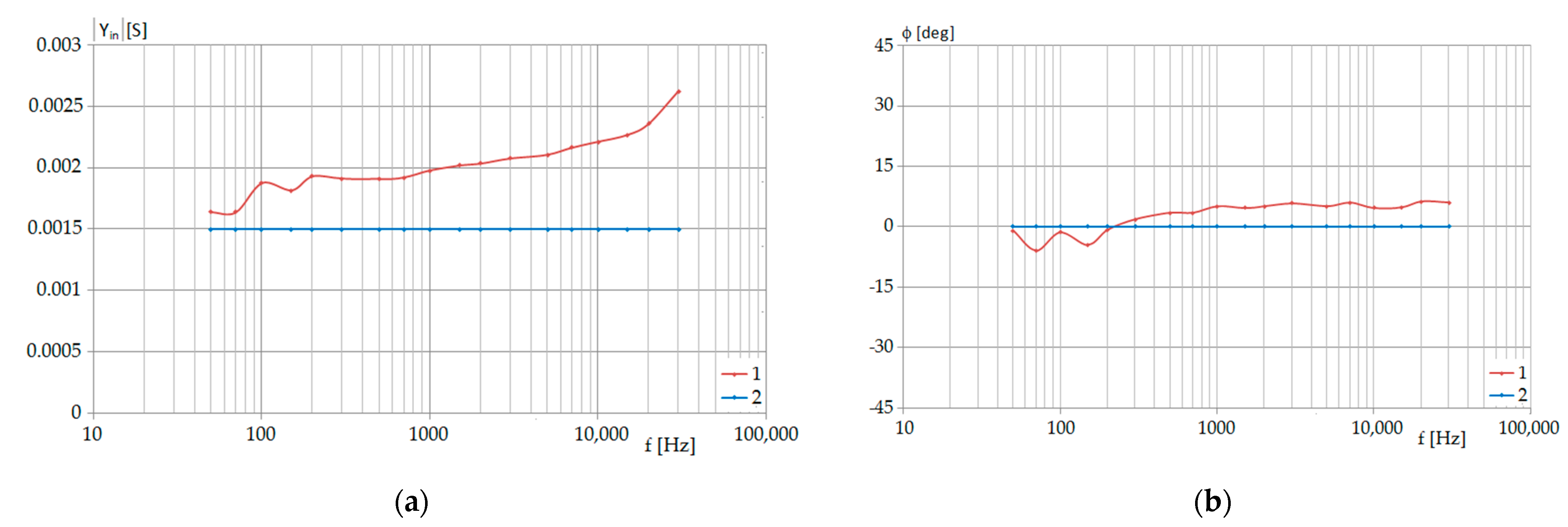
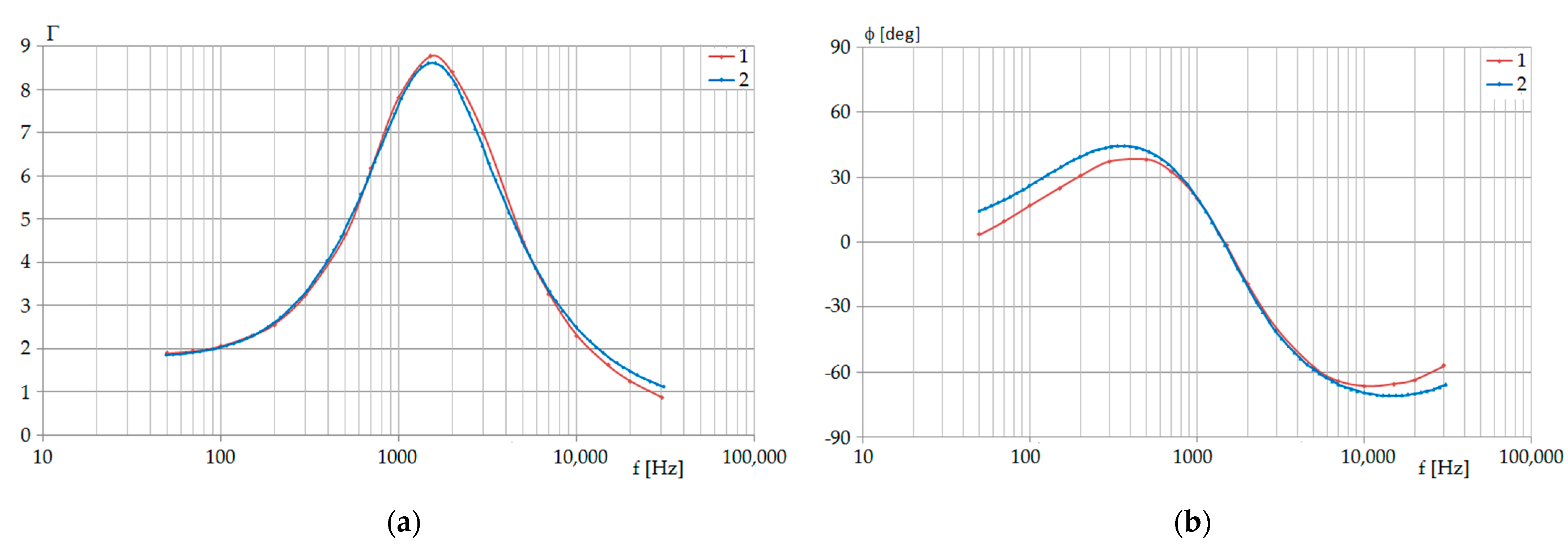
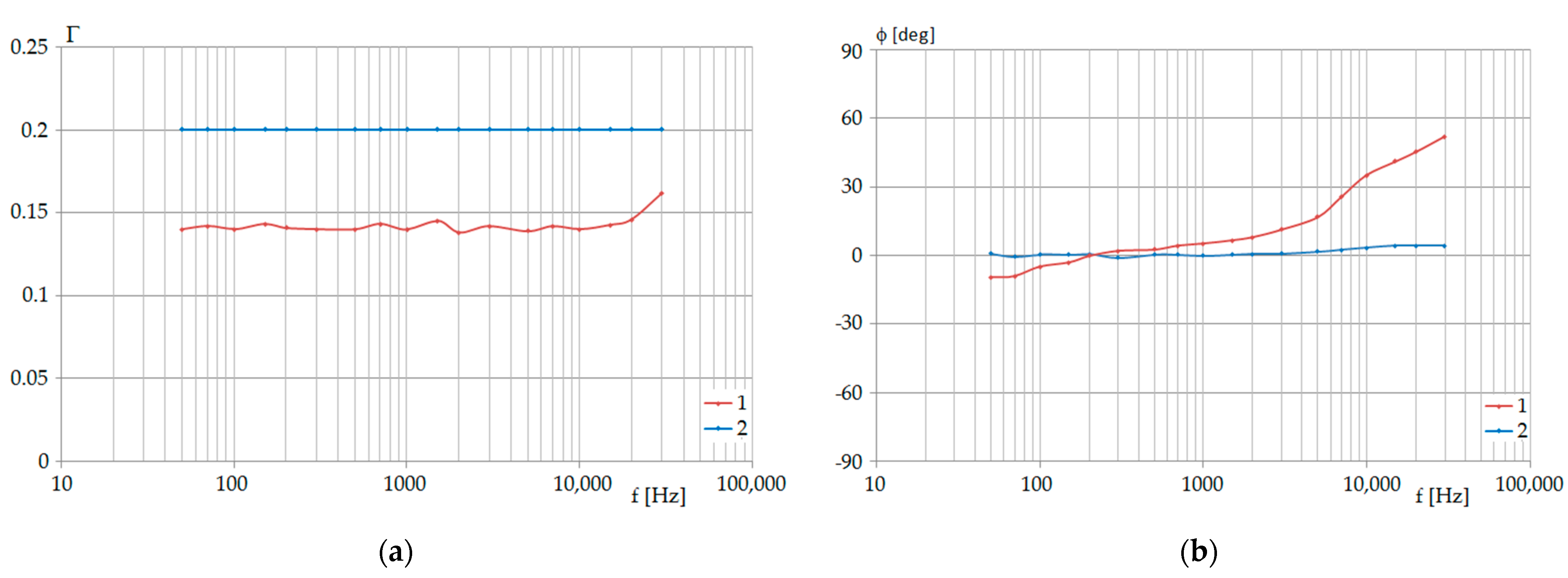
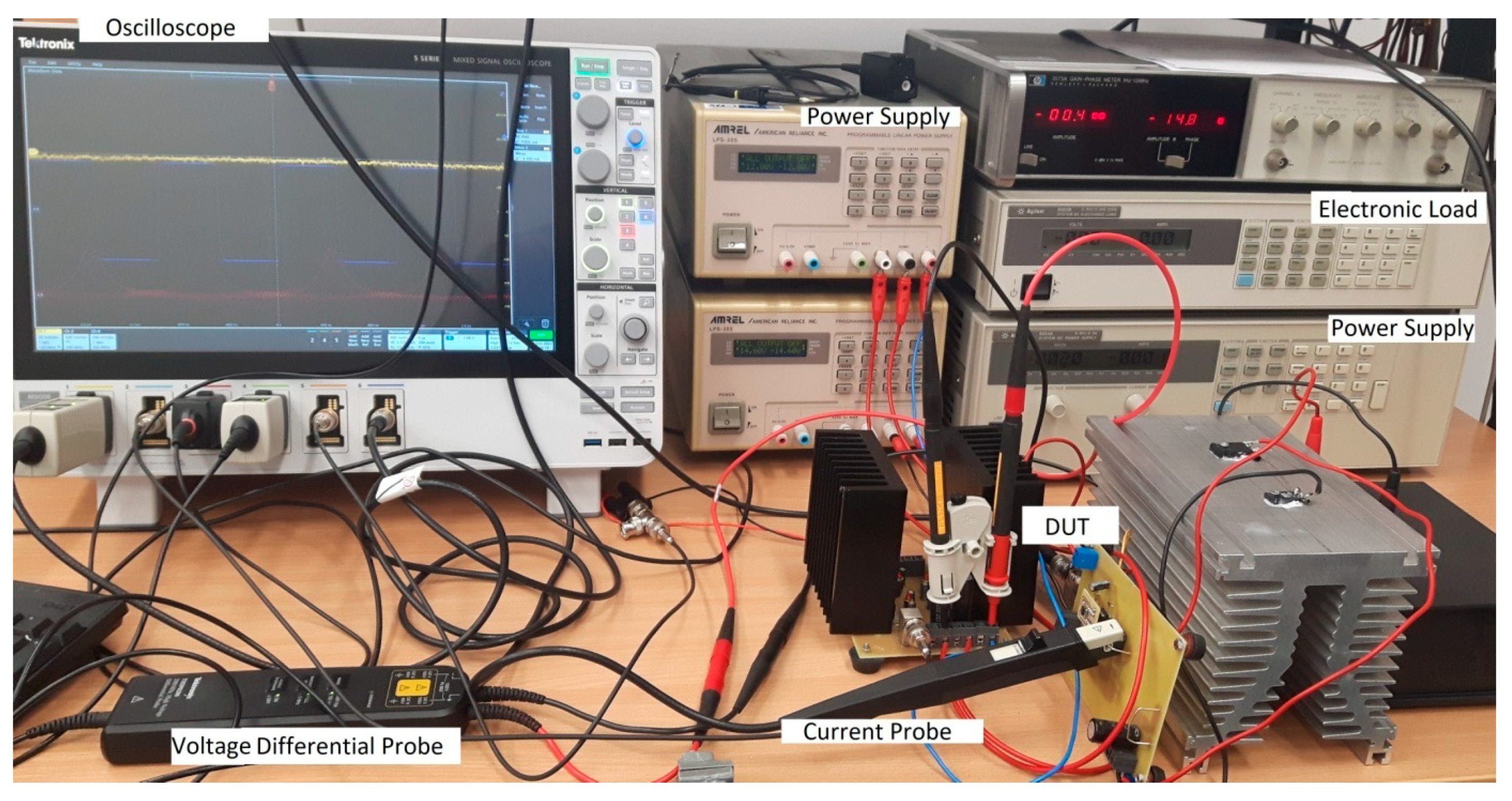
6. Calculations and Experimental Data

The following components were used in the laboratory converter models, which were subsequently used in the experiments. The BUCK and BOOST featured a MOSFET transistor NVD5867NLT4G with RT = 39 mΩ and a diode MBRS340 with RD = 281 mΩ. Other components of the BUCK converter were as follows: L = 90.8 µH, RL = 121.6 mΩ, C = 108.8 µF, RC = 18.6 mΩ. As for the BOOST converter: L =22.6 µH, RL = 35 mΩ, C = 321 µF, RC = 70 mΩ. The FLYBACK converter featured a HEMT transistor TPH3026 with RT = 167 mΩ, a diode MBRD1035 with RD = 200 mΩ, a transformer Coilcraft C1174-AL with n = 0.2, L = 150 µH, RL1 = 0.5 Ω, RL2= 23 mΩ, an output capacitor with C = 470 µF, RC = 76 mΩ. The above symbols are reported in Figure 1. The values were estimated by measurements. The conditions of the experiments are presented in Table 1. The switching frequency fS = 200 kHz was used in all experiments.
In the measurements and calculations of the input admittance, the input voltage of the form
v G = V G + V g m · sin ω t
at constant DA was applied. Similarly, in the measurements and calculations of Γ, the duty ratio
d A = D A + θ m · sin ω t
at constant VG was applied. In both cases, the input current was:
i G = I G + I g m · sin ( ω t + φ )
The magnitudes of Y and Γ were obtained as:
| Y | = I g m V g m
| Γ | = I g m θ g m
The results of the measurements and calculations based on the averaged models are presented in Figure 11, Figure 12, Figure 13, Figure 14, Figure 15, Figure 16, Figure 17, Figure 18, Figure 19, Figure 20, Figure 21 and Figure 22.
A substantial difference between the frequency characteristics of the input admittance of the buck converter in CCM and DCM was observed. The curves in Figure 11a for CCM correspond to the second-order form of the admittance, whereas the curves in Figure 12a correspond to the first-order frequency dependence of the numerator and denominator. Similar observations were made for the frequency characteristics of the Γ quantity.
The main features of the frequency characteristics of the boost converter were similar to those of the buck converter. The analysis of the characteristics of the input admittance and Γ magnitudes of the flyback converter working in DCM provided values independent of the frequency. The results of the measurements, presented in Figure 20 and Figure 22, exhibited some differences from the calculation results. These can be attributed to the greater influence of the parasitic resistances on the real input characteristics than in the case of the buck and boost converters.
The consistency of the calculations and measurements results was generally very good. The discrepancies observed in some cases may be attributed to the approximate character of the averaged models. An additional cause of differences in the calculations and measurements was the inaccuracy of the component parameters estimation.

7. Conclusions

The small-signal input characteristics of the power stage of the DC–DC converters buck, boost, and flyback, working in continuous conduction mode (CCM) and discontinuous conduction mode (DCM) are presented in this paper. The characteristics were obtained by calculations and by measurements. In the calculations, the formulas resulting from the models based on the separation of variables were applied and included the parasitic resistances of all components of the converters. The derivation of small-signal models and the formulas describing the input characteristics are presented in Section 2, Section 3, Section 4 and Section 5.
The small-signal averaged models of buck, boost, and flyback converters, derived with the separation of variables approach, are discussed in Section 2 and Section 3. The resulting small-signal input characteristics of these converters are presented in Section 4 for CCM and in Section 5 for DCM. Apart from the input admittance defined by Equation (18), the quantity Γ, representing the influence of the control signal on the input current, is defined by Equation (19) and was analyzed. Special attention was paid to the input characteristics of converters working in the discontinuous conduction mode (Section 5). It is shown that the quantities Y and Γ of the buck and boost converters in DCM are described by the first-order functions of s, whereas Y and Γ of the flyback converter in DCM are real numbers. These results differ from the descriptions based on the averaged models derived with the “switch averaging” approach. It should be noted that in the derivation of the formulas for DCM, the parasitic resistances of components were neglected, as described at the end of Section 1.
The analytical description of the input characteristics presented in Section 4 and Section 5 was verified by calculations and measurements, as shown in Section 5. The consistency of the measurements and calculations based on the presented formulas seems to be satisfactory. Future work will include a comparison of the small-signal models with the existing models in the frequency domain.

Author Contributions

Conceptualization, W.J.; methodology, M.B., J.K. and M.W.; software, M.B. and J.K.; validation, M.B., J.K. and M.W.; formal analysis, W.J.; investigation, W.J., M.B. and J.K.; resources, M.B., J.K. and M.W.; data curation, M.B.; writing—original draft preparation, W.J.; writing—review and editing, W.J., M.B., J.K. and M.W.; visualization, J.K.; supervision, W.J.; project administration, W.J.; funding acquisition, W.J. All authors have read and agreed to the published version of the manuscript.

Funding

This research received no external funding.

Institutional Review Board Statement

Not applicable.

Informed Consent Statement

Not applicable.

Data Availability Statement

Not applicable.

Conflicts of Interest

The authors declare no conflict of interest.

Appendix A

An example of a measurement set-up is presented in Figure A1. The list of devices used during the measurements is presented below:
  • Mixed Signal Oscilloscope (Tektronix MSO56)
  • Arbitrary Waveform Generator (Tektronix AFG31022)
  • Power Supply (Agilent 6674A/AMREL LPS-305)
  • Electronic Load (Agilent 6060B)
  • Current Probe (Tektronix TCP0030)
  • High-voltage Differential Probe (Tektronix THDP0200) and additionally
  • Automatic RCL Meter (Fluke PM6306)
Figure A1. Example of the measurement set-up.
Energies 15 01924 g0a1

References

  1. Erickson, R.W.; Maksimovic, D. Fundamentals of Power Electronics, 2nd ed.; Kluwer: Bangkok, Thailand, 2002. [Google Scholar]
  2. Kazimierczuk, M.K. Pulse-Width Modulated DC–DC Power Converters; J. Wiley: Hoboken, NJ, USA, 2008. [Google Scholar]
  3. Hart, D.W. Power Electronics; McGraw-Hill: New York, NY, USA, 2011. [Google Scholar]
  4. Middlebrook, R.D.; Čuk, S. A general unified approach to modeling switching-converter power stages. In Proceedings of the IEEE Power Electronic Specialists Conference, Cleveland, OH, USA, 8–10 June 1976; pp. 18–34. [Google Scholar]
  5. Čuk, S.; Middlebrook, R.D. A general unified approach to modelling switching DC-DC converters in discontinuous conduction mode. In Proceedings of the Power Electronic Specialists Conference, Piscataway, NJ, USA, 14–16 June 1977; pp. 18–34. [Google Scholar]
  6. Middlebrook, R.D. Small-Signal Modeling of Pulse-Width Modulated Switched-Mode Power Conwerters. Proc. IEEE 1988, 76, 343–354. [Google Scholar] [CrossRef] [Green Version]
  7. Vorperian, V. Simplified analysis of PWM converters using model of PWM Switch. Continuous conduction mode. IEEE Trans. Aerosp. Electron. Syst. 1990, 26, 490–496. [Google Scholar] [CrossRef]
  8. Vorperian, V. Simplified analysis of PWM converters using model of PWM switch, II. Discontinuous conduction mode. IEEE Trans. Aerosp. Electron. Syst. 1990, 26, 497–505. [Google Scholar] [CrossRef]
  9. Maksimowic, D.; Stankovic, A.M.; Thottuvelil, V.J.; Verghese, G.C. Modeling and Simulation of Power Electronic Converters. Proc. IEEE 2011, 89, 898–912. [Google Scholar] [CrossRef]
  10. Janke, W. Averaged Models of Pulse-Modulated DC-DC Converters, Part I. Discussion of standard methods. Arch. Electr. Eng. 2012, 61, 609–631. [Google Scholar]
  11. Ochoa, D.; Lázaro, A.; Zumel, P.; Sanz, M.; Rodriguez de Frutos, J.; Barrado, A. Small-Signal Modeling of Phase-Shifted Full-Bridge Converter Considering the Delay Associated to the Leakage Inductance. Energies 2021, 14, 7280. [Google Scholar] [CrossRef]
  12. Rasheduzzaman, M.; Fajri, P.; Kimball, J.; Deken, B. Modeling, Analysis, and Control Design of a Single-Stage Boost Inverter. Energies 2021, 14, 4098. [Google Scholar] [CrossRef]
  13. De Gusseme, K.; Van de Sype, D.M.; Van den Bossche, A.P.M.; Melkebeek, J.A. Variable-Duty-Cycle Control to Achieve High Input Power Factor for DCM Boost PFC Converter. IEEE Trans. Ind. Electron. 2007, 54, 858–865. [Google Scholar] [CrossRef]
  14. Enrique, J.M.; Duran, E.; Sidrach-de-Cardona, M.; Andujar, J.M. Theoretical assessment of the maximum power point tracking efficiency of photovoltaic facilities with different converter topologies. Elsevier Ltd Sol. Energy 2007, 81, 31–38. [Google Scholar] [CrossRef]
  15. Li, Y.; Oruganti, R. A Low Cost High Efficiency Inverter for Photovoltaic AC Module Application. In Proceedings of the 2010 35th IEEE Photovoltaic Specialists Conference, Honolulu, HI, USA, 20–25 June 2010; pp. 2853–2858. [Google Scholar]
  16. Lim, S.F.; Khambadkone, A.M. A Simple Digital DCM Control Scheme for Boost PFC Operating in Both CCM and DCM. IEEE Trans. Ind. Electron. 2011, 47, 1802–1812. [Google Scholar] [CrossRef]
  17. Middlebrook, R.D. Input filter considerations in design and applications of switching regulators. In Proceedings of the IEEE–IAS Annual Meeting, Chicago, IL, USA, 11–14 October 1976; pp. 366–382. [Google Scholar]
  18. Kazimierczuk, M.K.; Cravens, R.; Reatti, A. Closed-loop input impedance of PWM buck-derived DC-DC converters. In Proceedings of the IEEE International Symposium on Circuits and Systems, London, UK, 30 May–2 June 1994; pp. 61–64. [Google Scholar]
  19. Kim, D.; Son, D.; Choi, B. Input Impedance Analysis of PWM DC-to-DC Converters. In Proceedings of the IEEE 21st APEC, Dallas, TX, USA, 19–23 March 2006; pp. 1339–1346. [Google Scholar]
  20. Ahmadi, R.; Paschedag, D.; Ferdowsi, M. Closed Loop Input and Output Impedances of DC-DC Switching Converters Operating in Voltage and Current Mode Control. In Proceedings of the 36th Annual Conference of IEEE Industrial Electronic Society, Glendale, AZ, USA, 7–10 November 2010; pp. 2311–2316. [Google Scholar]
  21. Pidaparthy, S.K.; Choi, B. Input Impedances of DC-DC Converters: Unified Analysis and Application Example. J. Power Electron. 2016, 16, 2045–2056. [Google Scholar] [CrossRef]
  22. Zhang, X. Impedance Control and Stability of DC-DC Converter Systems. Ph.D. Thesis, University of Sheffield, Sheffield, UK, 2016. [Google Scholar]
  23. Asadi, F.; Eguchi, K. On the Extraction of Input and Output Impedance of PWM DC-DC Converters. Balk. J. Electr. Comput. Eng. 2019, 7, 123–130. [Google Scholar] [CrossRef]
  24. Janke, W. Averaged Models of Pulse-Modulated DC-DC Converters, Part II. Models Based on the Separation of Variables. Arch. Electr. Eng. 2012, 61, 633–654. [Google Scholar] [CrossRef]
  25. Janke, W. Equivalent circuits for averaged description of DC-DC switch-mode power converters based on separation of variables approach. Bull. Pol. Acad. Sci. 2013, 61, 711–723. [Google Scholar] [CrossRef] [Green Version]
  26. Janke, W.; Walczak, M. Small-Signal Input Characteristics of Step-Down and Step-Up Converters in Various Conduction Modes. Bull. Pol. Acad. Sci. 2016, 64, 265–270. [Google Scholar] [CrossRef] [Green Version]
  27. Sun, J.; Mitchell, D.; Greuel, M.; Krein, P.; Bass, R. Averaged modeling of PWM Converters Operating in Discontinuous Conduction Mode. IEEE Trans. Power Electron. 2001, 16, 482–492. [Google Scholar]
  28. Usman Iftikhar, M.; Lefranc, P.; Sadarnac, D.; Karimi, C. Theoretical and Experimental Investigation of Averaged Modeling of Non-ideal PWM DC-DC Converters Operating in DCM. In Proceedings of the IEEE Annual Power Electronics Specialists Conference, Rhodes, Greece, 15–19 June 2008. [Google Scholar]
  29. Janke, W.; Bączek, M.; Kraśniewski, J. The influence of parasitic effects on the selected features of switch-mode Flyback converter. Prz. Elektrotech. 2018, 94, 44–46. [Google Scholar]
  30. Janke, W.; Bączek, M.; Kraśniewski, J. Input characteristics of a non-ideal DC-DC flyback converter. Bull. Pol. Acad. Sci. 2019, 67, 841–849. [Google Scholar]
  31. Janke, W.; Bączek, M.; Kraśniewski, J. Large-signal input characteristics of selected DC–DC switching converters Part I. Continuous conduction mode. Arch. Electr. Eng. 2020, 69, 739–750. [Google Scholar]
  32. Janke, W.; Bączek, M.; Kraśniewski, J. Large-signal input characteristics of selected DC–DC switching converters, Part II. Discontinuous conduction mode. Arch. Electr. Eng. 2020, 69, 801–813. [Google Scholar]
Figure 1. Power stages of (a) buck, (b) boost, and (c) flyback converters.
Energies 15 01924 g001
Figure 2. Small-signal averaged model of a buck converter in CCM. Adapted from Ref. [25].
Energies 15 01924 g002
Figure 3. Small-signal averaged model of a boost converter in CCM. Adapted from Ref. [25].
Energies 15 01924 g003
Figure 4. Structure of the small-signal averaged models of non-ideal converters in DCM.
Energies 15 01924 g004
Figure 5. Large-signal averaged model of a flyback converter working in CCM. Adapted from Ref. [31].
Energies 15 01924 g005
Figure 6. Large-signal averaged model of a flyback converter working in DCM. Adapted from Ref. [32].
Energies 15 01924 g006
Figure 7. Large-signal model of a flyback converter in CCM for dA = const = DA.
Energies 15 01924 g007
Figure 8. Large-signal model of a flyback converter in CCM for vG = const = VG.
Energies 15 01924 g008
Figure 9. Simplified small-signal model of a flyback converter in CCM for θ = 0.
Energies 15 01924 g009
Figure 10. Simplified small-signal model of a flyback converter in CCM for Vg = 0.
Energies 15 01924 g010
Figure 11. Magnitude (a) and phase (b) of the input admittance of the BUCK converter in CCM: curves 1, measurements, curves 2, calculations according to Equation (20).
Energies 15 01924 g011
Figure 12. Magnitude (a) and phase (b) of the input admittance of the BUCK converter in DCM: curves 1, measurements, curves 2, calculations according to Equation (34).
Energies 15 01924 g012
Figure 13. Magnitude (a) and phase (b) of Γ of a BUCK converter in CCM: curves 1, measurements, curves 2, calculations according to Equation (21).
Energies 15 01924 g013
Figure 14. Magnitude (a) and phase (b) of Γ of the BUCK converter in DCM: curves 1, measurements, curves 2, calculations according to Equation (21).
Energies 15 01924 g014
Figure 15. Magnitude (a) and phase (b) of the input admittance of the BOOST converter in CCM: curves 1, measurements, curves 2, calculations according to Equation (24).
Energies 15 01924 g015
Figure 16. Magnitude (a) and phase (b) of the input admittance of the BOOST converter in DCM: curves 1, measurements, curves 2, calculations according to Equation (34).
Energies 15 01924 g016
Figure 17. Magnitude (a) and phase (b) of Γ of the BOOST converter in CCM: curves 1, measurements, curves 2, calculations according to Equation (25).
Energies 15 01924 g017
Figure 18. Magnitude (a) and phase (b) of Γ of the BOOST converter in DCM: curves 1, measurements, curves 2, calculations according to Equation (35).
Energies 15 01924 g018
Figure 19. Magnitude (a) and phase (b) of the input admittance of the FLYBACK converter in CCM: curves 1, measurements, curves 2, calculations according to Equation (28).
Energies 15 01924 g019
Figure 20. Magnitude (a) and phase (b) of the input admittance of the FLYBACK converter in DCM: curves 1, measurements, curves 2, calculations according to Equation (47).
Energies 15 01924 g020
Figure 21. Magnitude (a) and phase (b) of Γ of the FLYBACK converter in CCM: curves 1, measurements, curves 2, calculations according to Equation (25).
Energies 15 01924 g021
Figure 22. Magnitude (a) and phase (b) of Γ of the FLYBACK converter in DCM: curves 1, measurements, curves 2, calculations according to Equation (48).
Energies 15 01924 g022
Table 1. Experiment conditions.
ConverterModeVG [V]Vgm[mV]DAθmR [Ω]
BUCKCCM10500.40.0110
DCM10500.30.01198
BOOSTCCM5500.30.0110
DCM5500.30.01198
FLYBACKCCM202000.50.013
DCM202000.30.0150
Publisher’s Note: MDPI stays neutral with regard to jurisdictional claims in published maps and institutional affiliations.

